low-power bidirectional i2c isolators (rev. b) - texas instruments
TRANSCRIPT
Iso
lati
on
Ca
pa
cito
r
VCC2VCC1
SDA2SDA1
GND1 GND2
VREF
or SCL2or SCL1
Product
Folder
Sample &Buy
Technical
Documents
Tools &
Software
Support &Community
ReferenceDesign
ISO1540, ISO1541SLLSEB6C –JULY 2012–REVISED JUNE 2015
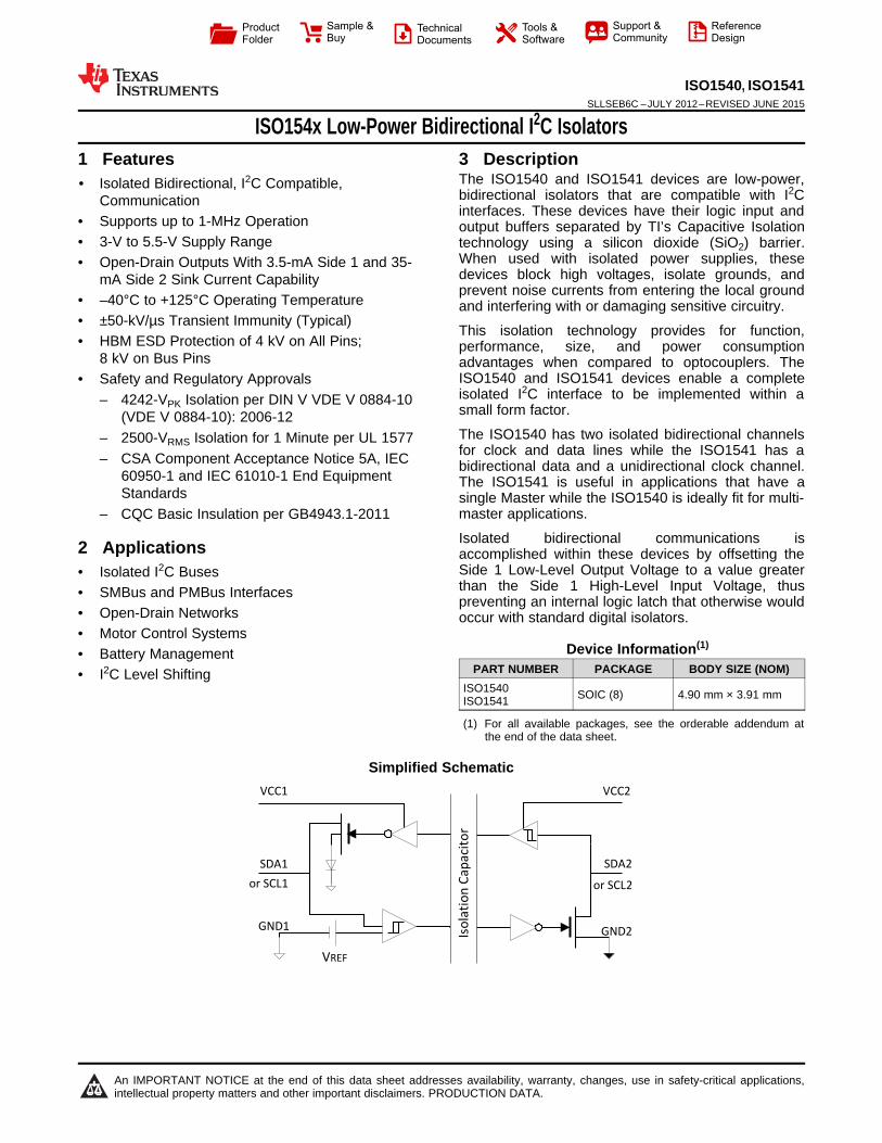
ISO154x Low-Power Bidirectional I2C Isolators1 Features 3 Description
The ISO1540 and ISO1541 devices are low-power,1• Isolated Bidirectional, I2C Compatible,
bidirectional isolators that are compatible with I2CCommunicationinterfaces. These devices have their logic input and
• Supports up to 1-MHz Operation output buffers separated by TI’s Capacitive Isolation• 3-V to 5.5-V Supply Range technology using a silicon dioxide (SiO2) barrier.
When used with isolated power supplies, these• Open-Drain Outputs With 3.5-mA Side 1 and 35-devices block high voltages, isolate grounds, andmA Side 2 Sink Current Capabilityprevent noise currents from entering the local ground
• –40°C to +125°C Operating Temperature and interfering with or damaging sensitive circuitry.• ±50-kV/µs Transient Immunity (Typical)
This isolation technology provides for function,• HBM ESD Protection of 4 kV on All Pins; performance, size, and power consumption
8 kV on Bus Pins advantages when compared to optocouplers. TheISO1540 and ISO1541 devices enable a complete• Safety and Regulatory Approvalsisolated I2C interface to be implemented within a– 4242-VPK Isolation per DIN V VDE V 0884-10small form factor.(VDE V 0884-10): 2006-12The ISO1540 has two isolated bidirectional channels– 2500-VRMS Isolation for 1 Minute per UL 1577for clock and data lines while the ISO1541 has a– CSA Component Acceptance Notice 5A, IEC bidirectional data and a unidirectional clock channel.
60950-1 and IEC 61010-1 End Equipment The ISO1541 is useful in applications that have aStandards single Master while the ISO1540 is ideally fit for multi-
master applications.– CQC Basic Insulation per GB4943.1-2011
Isolated bidirectional communications is2 Applications accomplished within these devices by offsetting theSide 1 Low-Level Output Voltage to a value greater• Isolated I2C Busesthan the Side 1 High-Level Input Voltage, thus• SMBus and PMBus Interfaces preventing an internal logic latch that otherwise would
• Open-Drain Networks occur with standard digital isolators.• Motor Control Systems
Device Information(1)• Battery Management
PART NUMBER PACKAGE BODY SIZE (NOM)• I2C Level ShiftingISO1540 SOIC (8) 4.90 mm × 3.91 mmISO1541
(1) For all available packages, see the orderable addendum atthe end of the data sheet.
Simplified Schematic
1
An IMPORTANT NOTICE at the end of this data sheet addresses availability, warranty, changes, use in safety-critical applications,intellectual property matters and other important disclaimers. PRODUCTION DATA.
ISO1540, ISO1541SLLSEB6C –JULY 2012–REVISED JUNE 2015 www.ti.com
Table of Contents9.2 Functional Block Diagrams ..................................... 121 Features .................................................................. 19.3 Feature Description................................................. 142 Applications ........................................................... 19.4 Device Functional Modes........................................ 163 Description ............................................................. 1
10 Application and Implementation........................ 174 Revision History..................................................... 210.1 Application Information.......................................... 175 Device Comparison Table ..................................... 310.2 Typical Application ................................................ 206 Pin Configuration and Functions ......................... 3
11 Power Supply Recommendations ..................... 227 Specifications......................................................... 312 Layout................................................................... 237.1 Absolute Maximum Ratings ...................................... 3
12.1 Layout Guidelines ................................................. 237.2 ESD Ratings.............................................................. 412.2 Layout Example .................................................... 237.3 Recommended Operating Conditions....................... 4
13 Device and Documentation Support ................. 247.4 Thermal Information .................................................. 413.1 Documentation Support ........................................ 247.5 Electrical Characteristics........................................... 513.2 Related Links ........................................................ 247.6 Timing Requirements ................................................ 613.3 Community Resources.......................................... 247.7 Switching Characteristics .......................................... 613.4 Trademarks ........................................................... 247.8 Typical Characteristics .............................................. 713.5 Electrostatic Discharge Caution............................ 248 Parameter Measurement Information ................ 1013.6 Glossary ................................................................ 249 Detailed Description ............................................ 12
14 Mechanical, Packaging, and Orderable9.1 Overview ................................................................. 12 Information ........................................................... 24
4 Revision HistoryNOTE: Page numbers for previous revisions may differ from page numbers in the current version.
Changes from Revision B (May 2013) to Revision C Page
• Added Pin Configuration and Functions section, ESD Ratings table, Feature Description section, Device FunctionalModes, Application and Implementation section, Power Supply Recommendations section, Layout section, Deviceand Documentation Support section, and Mechanical, Packaging, and Orderable Information section .............................. 1
• VDE Standard changed to DIN V VDE V 0884-10 (VDE V 0884-10): 2006-12 .................................................................... 1
Changes from Revision A (October 2012) to Revision B Page
• Change Safety Feature From: (VDE 0884 Part 2) (Pending) To: (VDE 0884 Part 2) (Approved)......................................... 1• Changed, VDE column From: File number: 40016131 (pending) To: File number: 40016131............................................ 16
Changes from Original (July 2012) to Revision A Page
• Changed From: CSA Component Acceptance Notice 5A (Pending) To: CSA Component Acceptance Notice 5A(Approved) .............................................................................................................................................................................. 1
• Changed From: IEC 60950-1 and IEC 61010-1 End Equipment Standards (Pending) To: IEC 60950-1 and IEC61010-1 End Equipment Standards (Approved)..................................................................................................................... 1
• Changed Regulatory Information, CSA column From: File number: 220991 (pending) To: File number: 220991 .............. 16
2 Submit Documentation Feedback Copyright © 2012–2015, Texas Instruments Incorporated
Product Folder Links: ISO1540 ISO1541
ISO1540 ISO1541
1
2
3
4 5
6
7
8
GND2
SCL1
VCC2VCC1
SCL2
GND1
SDA1 SDA2
Side 1 Side 2
Iso
lati
on
1
2
3
4 5
6
7
8
GND2
SCL1
VCC2VCC1
SCL2
GND1
SDA1 SDA2
Side 1 Side 2
Iso
lati
on
ISO1540, ISO1541www.ti.com SLLSEB6C –JULY 2012–REVISED JUNE 2015
5 Device Comparison Table
PRODUCT RATED ISOLATION PACKAGE CHANNEL DIRECTIONBoth SDA and SCLISO1540 are bidirectional4242-VPK and D-82500-VRMS
(1) SDA is bidirectionalISO1541 SCL is unidirectional
(1) See Regulatory Information for detailed Isolation specifications.
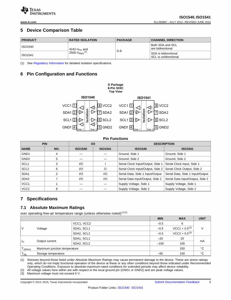
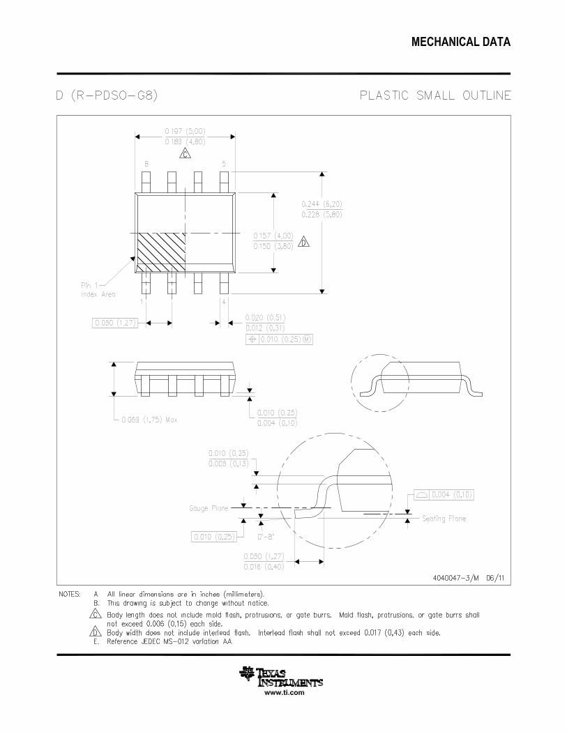
6 Pin Configuration and Functions
D Package8-Pin SOICTop View
Pin FunctionsPIN I/O DESCRIPTION
NAME NO. ISO1540 ISO1541 ISO1540 ISO1541GND1 4 — — Ground, Side 1 Ground, Side 1GND2 5 — — Ground, Side 2 Ground, Side 2SCL1 3 I/O I Serial Clock Input/Output, Side 1 Serial Clock Input, Side 1SCL2 6 I/O O Serial Clock Input/Output, Side 2 Serial Clock Output, Side 2SDA1 2 I/O I/O Serial Data, Side 1 Input/Output Serial Data, Side 1 Input/OutputSDA2 7 I/O I/O Serial Data Input/Output, Side 2 Serial Data Input/Output, Side 2VCC1 1 — — Supply Voltage, Side 1 Supply Voltage, Side 1VCC2 8 — — Supply Voltage, Side 2 Supply Voltage, Side 2
7 Specifications
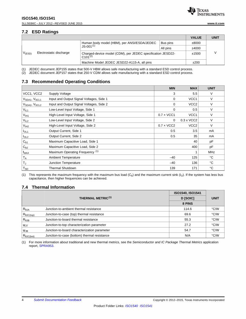
7.1 Absolute Maximum Ratingsover operating free-air temperature range (unless otherwise noted) (1) (2)
MIN MAX UNITVCC1, VCC2 –0.5 6
V Voltage SDA1, SCL1 –0.5 VCC1 + 0.5 (3) VSDA2, SCL2 –0.5 VCC2 + 0.5 (3)
SDA1, SCL1 –20 20IO Output current mA
SDA2, SCL2 –100 100TJ(MAX) Maximum junction temperature 150 °CTstg Storage temperature –65 150 °C
(1) Stresses beyond those listed under Absolute Maximum Ratings may cause permanent damage to the device. These are stress ratingsonly, which do not imply functional operation of the device at these or any other conditions beyond those indicated under RecommendedOperating Conditions. Exposure to absolute-maximum-rated conditions for extended periods may affect device reliability.
(2) All voltage values here within are with respect to the local ground pin (GND1 or GND2) and are peak voltage values.(3) Maximum voltage must not exceed 6 V.
Copyright © 2012–2015, Texas Instruments Incorporated Submit Documentation Feedback 3
Product Folder Links: ISO1540 ISO1541
ISO1540, ISO1541SLLSEB6C –JULY 2012–REVISED JUNE 2015 www.ti.com
7.2 ESD RatingsVALUE UNIT
Human body model (HBM), per ANSI/ESDA/JEDEC Bus pins ±8000JS-001 (1)
All pins ±4000V(ESD) Electrostatic discharge VCharged-device model (CDM), per JEDEC specification JESD22- ±1500
C101 (2)
Machine Model JEDEC JESD22-A115-A, all pins ±200
(1) JEDEC document JEP155 states that 500-V HBM allows safe manufacturing with a standard ESD control process.(2) JEDEC document JEP157 states that 250-V CDM allows safe manufacturing with a standard ESD control process.
7.3 Recommended Operating ConditionsMIN MAX UNIT
VCC1, VCC2 Supply Voltage 3 5.5 VVSDA1, VSCL1 Input and Output Signal Voltages, Side 1 0 VCC1 VVSDA2, VSCL2 Input and Output Signal Voltages, Side 2 0 VCC2 VVIL1 Low-Level Input Voltage, Side 1 0 0.5 VVIH1 High-Level Input Voltage, Side 1 0.7 × VCC1 VCC1 VVIL2 Low-Level Input Voltage, Side 2 0 0.3 x VCC2 VVIH2 High-Level Input Voltage, Side 2 0.7 × VCC2 VCC2 VIOL1 Output Current, Side 1 0.5 3.5 mAIOL2 Output Current, Side 2 0.5 35 mACb1 Maximum Capacitive Load, Side 1 40 pFCb2 Maximum Capacitive Load, Side 2 400 pFfMAX Maximum Operating Frequency (1) 1 MHzTA Ambient Temperature –40 125 °CTJ Junction Temperature –40 136 °CTSD Thermal Shutdown 139 171 °C
(1) This represents the maximum frequency with the maximum bus load (Cb) and the maximum current sink (IO). If the system has less buscapacitance, then higher frequencies can be achieved.
7.4 Thermal InformationISO1540, ISO1541
THERMAL METRIC (1) D [SOIC] UNIT8 PINS
RθJA Junction-to-ambient thermal resistance 114.6 °C/WRθJC(top) Junction-to-case (top) thermal resistance 69.6 °C/WRθJB Junction-to-board thermal resistance 55.3 °C/WψJT Junction-to-top characterization parameter 27.2 °C/WψJB Junction-to-board characterization parameter 54.7 °C/WRθJC(bot) Junction-to-case (bottom) thermal resistance N/A °C/W
(1) For more information about traditional and new thermal metrics, see the Semiconductor and IC Package Thermal Metrics applicationreport, SPRA953.
4 Submit Documentation Feedback Copyright © 2012–2015, Texas Instruments Incorporated
Product Folder Links: ISO1540 ISO1541
ISO1540, ISO1541www.ti.com SLLSEB6C –JULY 2012–REVISED JUNE 2015
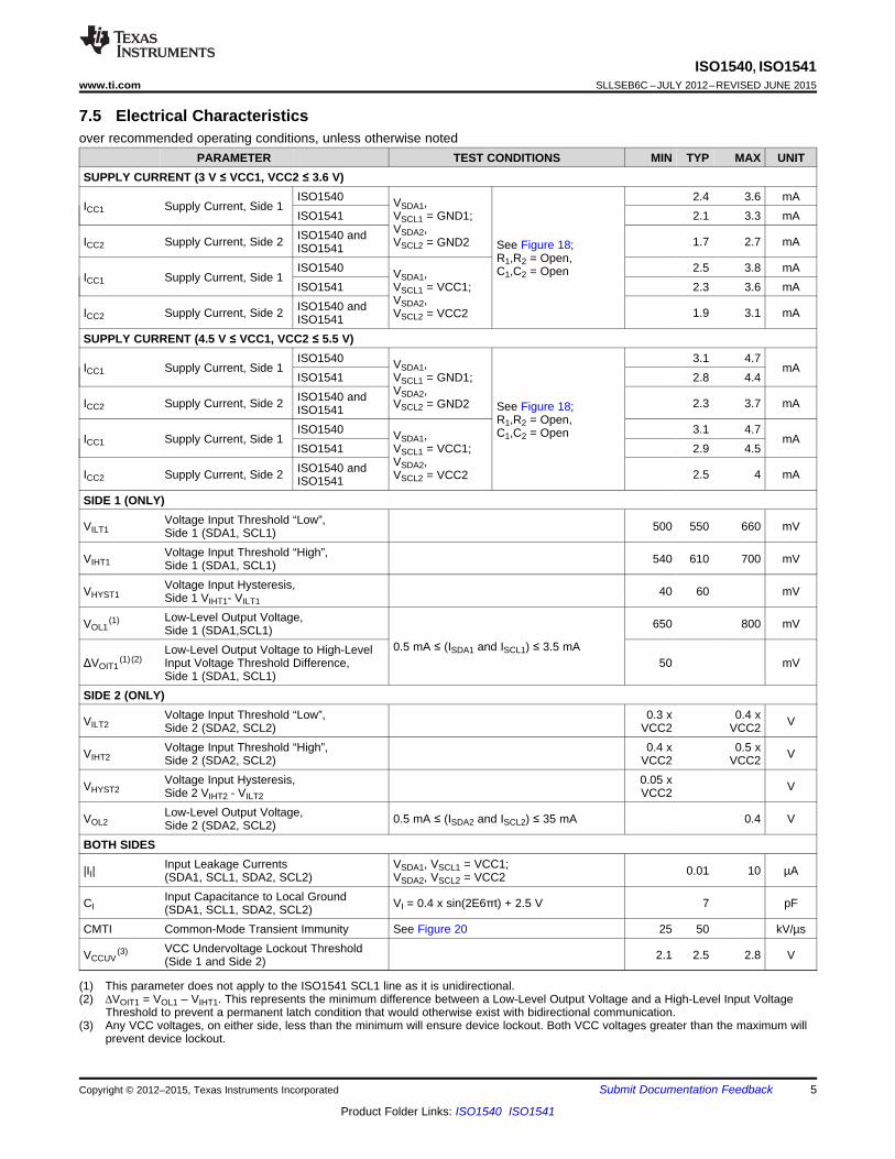
7.5 Electrical Characteristicsover recommended operating conditions, unless otherwise noted
PARAMETER TEST CONDITIONS MIN TYP MAX UNITSUPPLY CURRENT (3 V ≤ VCC1, VCC2 ≤ 3.6 V)
ISO1540 2.4 3.6 mAVSDA1,ICC1 Supply Current, Side 1ISO1541 VSCL1 = GND1; 2.1 3.3 mA
VSDA2,ISO1540 andICC2 Supply Current, Side 2 1.7 2.7 mAVSCL2 = GND2 See Figure 18;ISO1541R1,R2 = Open,
ISO1540 2.5 3.8 mAC1,C2 = OpenVSDA1,ICC1 Supply Current, Side 1ISO1541 VSCL1 = VCC1; 2.3 3.6 mA
VSDA2,ISO1540 andICC2 Supply Current, Side 2 1.9 3.1 mAVSCL2 = VCC2ISO1541SUPPLY CURRENT (4.5 V ≤ VCC1, VCC2 ≤ 5.5 V)
ISO1540 3.1 4.7VSDA1,ICC1 Supply Current, Side 1 mAISO1541 VSCL1 = GND1; 2.8 4.4
VSDA2,ISO1540 andICC2 Supply Current, Side 2 2.3 3.7 mAVSCL2 = GND2 See Figure 18;ISO1541R1,R2 = Open,
ISO1540 3.1 4.7C1,C2 = OpenVSDA1,ICC1 Supply Current, Side 1 mAISO1541 VSCL1 = VCC1; 2.9 4.5
VSDA2,ISO1540 andICC2 Supply Current, Side 2 2.5 4 mAVSCL2 = VCC2ISO1541SIDE 1 (ONLY)
Voltage Input Threshold “Low”,VILT1 500 550 660 mVSide 1 (SDA1, SCL1)Voltage Input Threshold “High”,VIHT1 540 610 700 mVSide 1 (SDA1, SCL1)Voltage Input Hysteresis,VHYST1 40 60 mVSide 1 VIHT1- VILT1
Low-Level Output Voltage,VOL1(1) 650 800 mVSide 1 (SDA1,SCL1)
0.5 mA ≤ (ISDA1 and ISCL1) ≤ 3.5 mALow-Level Output Voltage to High-LevelΔVOIT1
(1) (2) Input Voltage Threshold Difference, 50 mVSide 1 (SDA1, SCL1)
SIDE 2 (ONLY)Voltage Input Threshold “Low”, 0.3 x 0.4 xVILT2 VSide 2 (SDA2, SCL2) VCC2 VCC2Voltage Input Threshold “High”, 0.4 x 0.5 xVIHT2 VSide 2 (SDA2, SCL2) VCC2 VCC2Voltage Input Hysteresis, 0.05 xVHYST2 VSide 2 VIHT2 - VILT2 VCC2Low-Level Output Voltage,VOL2 0.5 mA ≤ (ISDA2 and ISCL2) ≤ 35 mA 0.4 VSide 2 (SDA2, SCL2)
BOTH SIDESInput Leakage Currents VSDA1, VSCL1 = VCC1;|II| 0.01 10 µA(SDA1, SCL1, SDA2, SCL2) VSDA2, VSCL2 = VCC2Input Capacitance to Local GroundCI VI = 0.4 x sin(2E6πt) + 2.5 V 7 pF(SDA1, SCL1, SDA2, SCL2)
CMTI Common-Mode Transient Immunity See Figure 20 25 50 kV/µsVCC Undervoltage Lockout ThresholdVCCUV
(3) 2.1 2.5 2.8 V(Side 1 and Side 2)
(1) This parameter does not apply to the ISO1541 SCL1 line as it is unidirectional.(2) ∆VOIT1 = VOL1 – VIHT1. This represents the minimum difference between a Low-Level Output Voltage and a High-Level Input Voltage
Threshold to prevent a permanent latch condition that would otherwise exist with bidirectional communication.(3) Any VCC voltages, on either side, less than the minimum will ensure device lockout. Both VCC voltages greater than the maximum will
prevent device lockout.
Copyright © 2012–2015, Texas Instruments Incorporated Submit Documentation Feedback 5
Product Folder Links: ISO1540 ISO1541
ISO1540, ISO1541SLLSEB6C –JULY 2012–REVISED JUNE 2015 www.ti.com
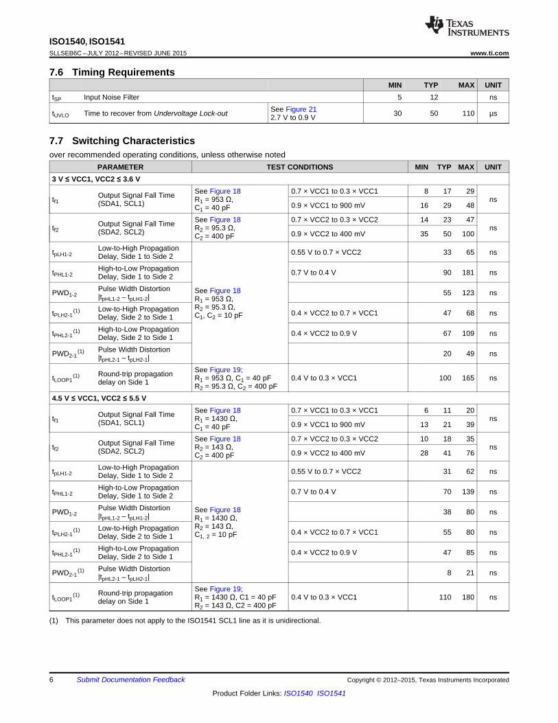
7.6 Timing RequirementsMIN TYP MAX UNIT
tSP Input Noise Filter 5 12 nsSee Figure 21tUVLO Time to recover from Undervoltage Lock-out 30 50 110 µs2.7 V to 0.9 V
7.7 Switching Characteristicsover recommended operating conditions, unless otherwise noted
PARAMETER TEST CONDITIONS MIN TYP MAX UNIT3 V ≤ VCC1, VCC2 ≤ 3.6 V
See Figure 18 0.7 × VCC1 to 0.3 × VCC1 8 17 29Output Signal Fall Timetf1 R1 = 953 Ω, ns(SDA1, SCL1) 0.9 × VCC1 to 900 mV 16 29 48C1 = 40 pFSee Figure 18 0.7 × VCC2 to 0.3 × VCC2 14 23 47Output Signal Fall Timetf2 R2 = 95.3 Ω, ns(SDA2, SCL2) 0.9 × VCC2 to 400 mV 35 50 100C2 = 400 pF
Low-to-High PropagationtpLH1-2 0.55 V to 0.7 × VCC2 33 65 nsDelay, Side 1 to Side 2High-to-Low PropagationtPHL1-2 0.7 V to 0.4 V 90 181 nsDelay, Side 1 to Side 2Pulse Width Distortion See Figure 18PWD1-2 55 123 ns|tpHL1-2 – tpLH1-2| R1 = 953 Ω,
R2 = 95.3 Ω,Low-to-High PropagationtPLH2-1(1) 0.4 × VCC2 to 0.7 × VCC1 47 68 nsC1, C2 = 10 pFDelay, Side 2 to Side 1
High-to-Low PropagationtPHL2-1(1) 0.4 × VCC2 to 0.9 V 67 109 nsDelay, Side 2 to Side 1
Pulse Width DistortionPWD2-1(1) 20 49 ns|tpHL2-1 – tpLH2-1|
See Figure 19;Round-trip propagationtLOOP1(1) R1 = 953 Ω, C1 = 40 pF 0.4 V to 0.3 × VCC1 100 165 nsdelay on Side 1 R2 = 95.3 Ω, C2 = 400 pF
4.5 V ≤ VCC1, VCC2 ≤ 5.5 VSee Figure 18 0.7 × VCC1 to 0.3 × VCC1 6 11 20Output Signal Fall Timetf1 R1 = 1430 Ω, ns(SDA1, SCL1) 0.9 × VCC1 to 900 mV 13 21 39C1 = 40 pFSee Figure 18 0.7 × VCC2 to 0.3 × VCC2 10 18 35Output Signal Fall Timetf2 R2 = 143 Ω, ns(SDA2, SCL2) 0.9 × VCC2 to 400 mV 28 41 76C2 = 400 pF
Low-to-High PropagationtpLH1-2 0.55 V to 0.7 × VCC2 31 62 nsDelay, Side 1 to Side 2High-to-Low PropagationtPHL1-2 0.7 V to 0.4 V 70 139 nsDelay, Side 1 to Side 2Pulse Width Distortion See Figure 18PWD1-2 38 80 ns|tpHL1-2 – tpLH1-2| R1 = 1430 Ω,
R2 = 143 Ω,Low-to-High PropagationtPLH2-1(1) 0.4 × VCC2 to 0.7 × VCC1 55 80 nsC1, 2 = 10 pFDelay, Side 2 to Side 1
High-to-Low PropagationtPHL2-1(1) 0.4 × VCC2 to 0.9 V 47 85 nsDelay, Side 2 to Side 1
Pulse Width DistortionPWD2-1(1) 8 21 ns|tpHL2-1 – tpLH2-1|
See Figure 19;Round-trip propagationtLOOP1(1) R1 = 1430 Ω, C1 = 40 pF 0.4 V to 0.3 × VCC1 110 180 nsdelay on Side 1 R2 = 143 Ω, C2 = 400 pF
(1) This parameter does not apply to the ISO1541 SCL1 line as it is unidirectional.
6 Submit Documentation Feedback Copyright © 2012–2015, Texas Instruments Incorporated
Product Folder Links: ISO1540 ISO1541
0
5
10
15
20
25
30
−40 −25 −10 5 20 35 50 65 80 95 110 125Free-Air Temperature (°C)
Fal
l Tim
e, t f
2 (n
s)
R2 = 95.3 ΩR2 = 2.2 kΩ
VCC2 = 3.3 VC2 = 400 pFFall Time measured from 70% to 30% VCC2
G003
0
5
10
15
20
25
30
−40 −25 −10 5 20 35 50 65 80 95 110 125Free-Air Temperature (°C)
Fal
l Tim
e, t f
2 (n
s)
R2 = 143 ΩR2 = 2.2 kΩ
VCC2 = 5 VC2 = 400 pFFall Time measured from 70% to 30% VCC2
G004
0
2
4
6
8
10
12
14
16
18
20
−40 −25 −10 5 20 35 50 65 80 95 110 125Free-Air Temperature (°C)
Fal
l Tim
e, t f
1 (n
s)
R1 = 953 ΩR1 = 2.2 kΩ
VCC1 = 3.3 VC1 = 40 pFFall Time measured from 70% to 30% VCC1
G001
0
2
4
6
8
10
12
14
16
18
20
−40 −25 −10 5 20 35 50 65 80 95 110 125Free-Air Temperature (°C)
Fal
l Tim
e, t f
1 (n
s)
R1 = 1430 ΩR1 = 2.2 kΩ
VCC1 = 5 VC1 = 40 pFFall Time measured from 70% to 30% VCC1
G002
0 0.3 0.6 0.9
Outp
ut C
urr
ent, I
(mA
)O
L1
Applied Voltage, V , V (V)SDA1 SCL1
0.1 0.2 0.4 0.5 0.7 0.8
-0.5
1.0
0.0
2.0
0.5
3.0
1.5
2.5T = 25 CA
o
Ou
tpu
t V
olta
ge
, V
(V)
OL
1
0.780
0.740
0.800
0.720
0.680
0.760
0.660
0.640
0.600
0.700
0.620
I = 3.5 mAOL1
I = 0.5 mAOL1
−40 −25 −10 5 20 35 50 65 80 95 110 125
Free−Air Temperature (°C)
ISO1540, ISO1541www.ti.com SLLSEB6C –JULY 2012–REVISED JUNE 2015
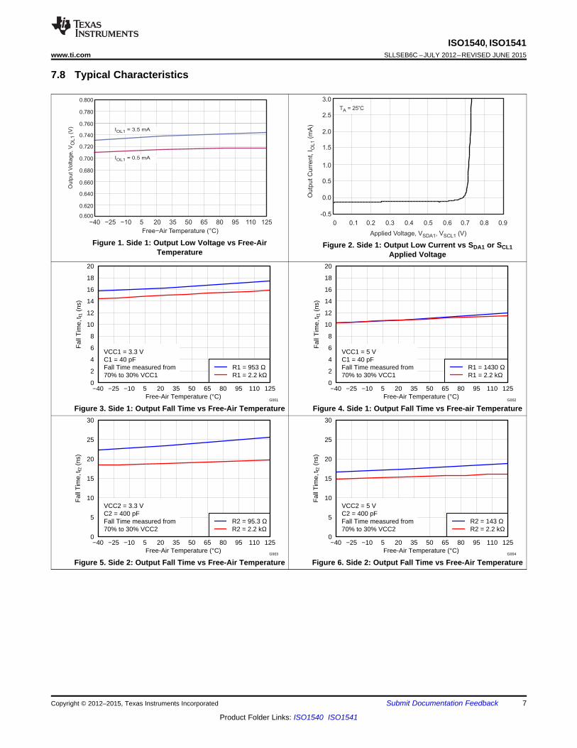
7.8 Typical Characteristics
Figure 1. Side 1: Output Low Voltage vs Free-Air Figure 2. Side 1: Output Low Current vs SDA1 or SCL1Temperature Applied Voltage
Figure 3. Side 1: Output Fall Time vs Free-Air Temperature Figure 4. Side 1: Output Fall Time vs Free-air Temperature
Figure 5. Side 2: Output Fall Time vs Free-Air Temperature Figure 6. Side 2: Output Fall Time vs Free-Air Temperature
Copyright © 2012–2015, Texas Instruments Incorporated Submit Documentation Feedback 7
Product Folder Links: ISO1540 ISO1541
0
10
20
30
40
50
60
70
−40 −25 −10 5 20 35 50 65 80 95 110 125Free-Air Temperature (°C)
Pro
paga
tion
Del
ay, t
PLH
2−1
(ns)
VCC1 and VCC2 = 3.3 V, R1 = 953 ΩVCC1 and VCC2 = 5 V, R1 = 1430 Ω
C1 = 10 pF
G009
0
10
20
30
40
50
60
70
80
−40 −25 −10 5 20 35 50 65 80 95 110 125Free-Air Temperature (°C)
Pro
paga
tion
Del
ay, t
PH
L2−1
(ns
)
VCC1 and VCC2 = 3.3 V, R1 = 953 ΩVCC1 and VCC2 = 5 V, R1 = 1430 Ω
C1 = 10 pF
G010
1000
1005
1010
1015
1020
1025
1030
1035
1040
1045
1050
−40 −25 −10 5 20 35 50 65 80 95 110 125Free-Air Temperature (°C)
Pro
paga
tion
Del
ay, t
PLH
1−2
(ns)
VCC1 and VCC2 = 3.3 VVCC1 and VCC2 = 5 V
R2 = 2.2 kΩC2 = 400 pF
G007
0
10
20
30
40
50
60
70
80
90
−40 −25 −10 5 20 35 50 65 80 95 110 125Free-Air Temperature (°C)
Pro
paga
tion
Del
ay, t
PH
L1−2
(ns
)
VCC1 and VCC2 = 3.3 VVCC1 and VCC2 = 5 V
R2 = 2.2 kΩC2 = 400 pF
G008
0
5
10
15
20
25
30
35
40
45
−40 −25 −10 5 20 35 50 65 80 95 110 125Free-Air Temperature (°C)
Pro
paga
tion
Del
ay, t
PLH
1−2
(ns)
VCC1 and VCC2 = 3.3 V, R2 = 95.3 ΩVCC1 and VCC2 = 5 V, R2 = 143 Ω
C2 = 10 pF
G005
0
20
40
60
80
100
120
−40 −25 −10 5 20 35 50 65 80 95 110 125Free-Air Temperature (°C)
Pro
paga
tion
Del
ay, t
PH
L1−2
(ns
)
VCC1 and VCC2 = 3.3 V, R2 = 95.3 ΩVCC1 and VCC2 = 5 V, R2 = 143 Ω
C2 = 10 pF
G006
ISO1540, ISO1541SLLSEB6C –JULY 2012–REVISED JUNE 2015 www.ti.com
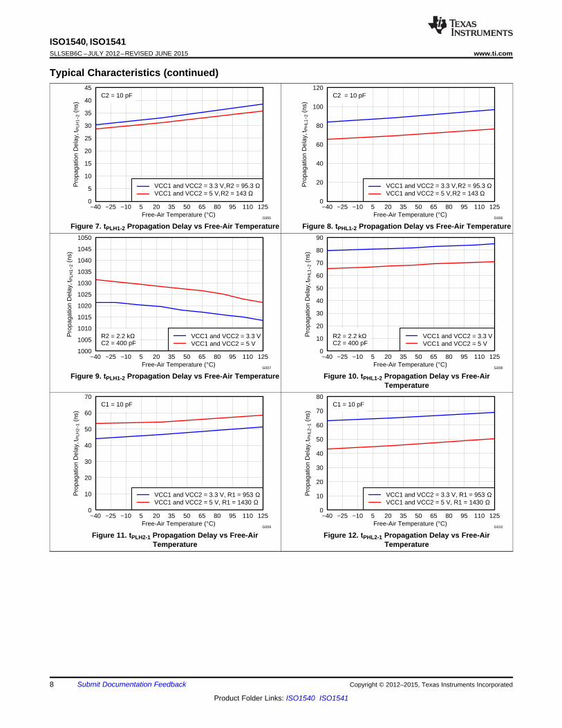
Typical Characteristics (continued)
Figure 7. tPLH1-2 Propagation Delay vs Free-Air Temperature Figure 8. tPHL1-2 Propagation Delay vs Free-Air Temperature
Figure 9. tPLH1-2 Propagation Delay vs Free-Air Temperature Figure 10. tPHL1-2 Propagation Delay vs Free-AirTemperature
Figure 11. tPLH2-1 Propagation Delay vs Free-Air Figure 12. tPHL2-1 Propagation Delay vs Free-AirTemperature Temperature
8 Submit Documentation Feedback Copyright © 2012–2015, Texas Instruments Incorporated
Product Folder Links: ISO1540 ISO1541
0
10
20
30
40
50
60
70
−40 −25 −10 5 20 35 50 65 80 95 110 125Free-Air Temperature (°C)
CM
TI (
kV/µ
s)
VCC1 and VCC2 = 3.3 VVCC1 and VCC2 = 5 V
G015
0
20
40
60
80
100
120
140
−40 −25 −10 5 20 35 50 65 80 95 110 125Free-Air Temperature (°C)
t LO
OP
1 (n
s)
VCC1 and VCC2 = 3.3 V, R1 = 953Ω, R2 = 95.3ΩVCC1 and VCC2 = 5 V, R1 = 1430Ω, R2 = 143Ω
C1 = 40 pFC2 = 400 pF
G013
575
580
585
590
595
600
−40 −25 −10 5 20 35 50 65 80 95 110 125Free-Air Temperature (°C)
t LO
OP
1 (n
s)
VCC1 and VCC2 = 3.3 VVCC1 and VCC2 = 5 V
R1 = 2.2 kΩC1 = 40 pFR2 = 2.2 kΩC2 = 400 pF
G014
132
134
136
138
140
142
144
146
148
−40 −25 −10 5 20 35 50 65 80 95 110 125Free-Air Temperature (°C)
Pro
paga
tion
Del
ay, t
PLH
2−1
(ns)
VCC1 and VCC2 = 3.3 VVCC1 and VCC2 = 5 V
R1 = 2.2 kΩC1 = 40 pF
G011
0
10
20
30
40
50
60
70
80
−40 −25 −10 5 20 35 50 65 80 95 110 125Free-Air Temperature (°C)
Pro
paga
tion
Del
ay, t
PH
L2−1
(ns
)
VCC1 and VCC2 = 3.3 VVCC1 and VCC2 = 5 V
R1 = 2.2 kΩC1 = 40 pF
G012
ISO1540, ISO1541www.ti.com SLLSEB6C –JULY 2012–REVISED JUNE 2015
Typical Characteristics (continued)
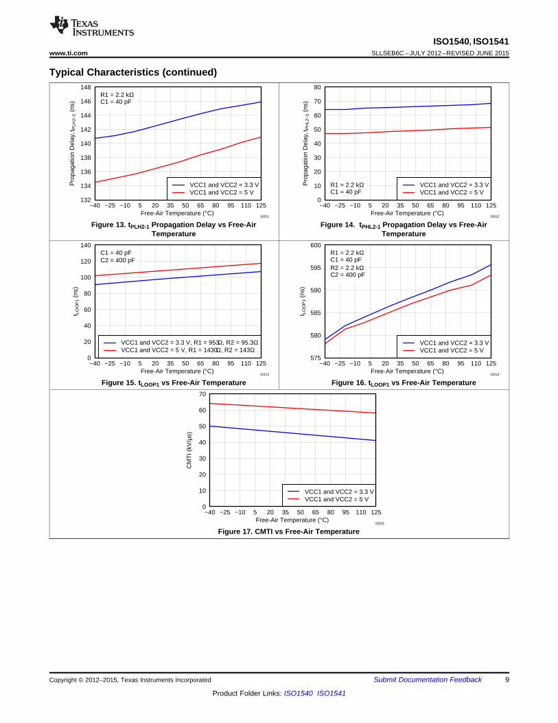
Figure 13. tPLH2-1 Propagation Delay vs Free-Air Figure 14. tPHL2-1 Propagation Delay vs Free-AirTemperature Temperature
Figure 15. tLOOP1 vs Free-Air Temperature Figure 16. tLOOP1 vs Free-Air Temperature
Figure 17. CMTI vs Free-Air Temperature
Copyright © 2012–2015, Texas Instruments Incorporated Submit Documentation Feedback 9
Product Folder Links: ISO1540 ISO1541
VCMTI
Input
+
Output
-
GNDx GNDy
2 kW
VCCx VCCy
Isola
tion
2 kW
Isola
tion
+
-
GND1 GND2
VCC1
R2
VCC2
SDA1 or
SCL1
Output
R1
C2C1
VCC1
GND1
0.3VCC1
tLOOP1
0.4V
SDA1
SCL1 [ISO1540 Only]
SDA1
R1 R1
C1 C1
ISO1540/1
VCC1
R2R2
C2C2
VCC2
SCL1
SDA2
SCL2
-+
-+
ISO1540, ISO1541SLLSEB6C –JULY 2012–REVISED JUNE 2015 www.ti.com
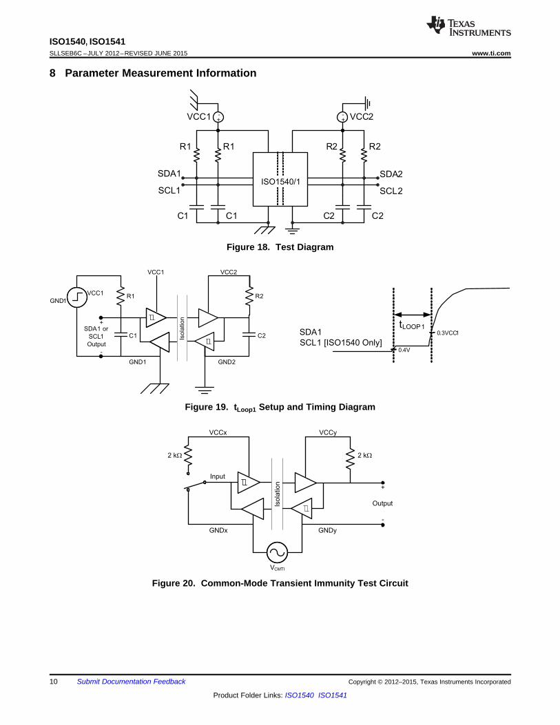
8 Parameter Measurement Information
Figure 18. Test Diagram
Figure 19. tLoop1 Setup and Timing Diagram
Figure 20. Common-Mode Transient Immunity Test Circuit
10 Submit Documentation Feedback Copyright © 2012–2015, Texas Instruments Incorporated
Product Folder Links: ISO1540 ISO1541
Isola
tio
n
+
Output
-
GNDx GNDy
VCCx
Ry
VCCy
Isola
tion
SDAx or
SCLx
+
Output
-
GNDx GNDy
VCCx
Ry
VCCy
0 V
Side x, Side y VCCx,VCCy Ry
1, 2 3.3 V, 3.3 V 95.3 Ω
2, 1 3.3 V, 3.3 V 953 Ω
or
VCCx or
VCCy
Output
SDAx orSCLx
2.7 V
0.9 V
tUVLO
VCCy
0 V
VCCx
ISO1540, ISO1541www.ti.com SLLSEB6C –JULY 2012–REVISED JUNE 2015
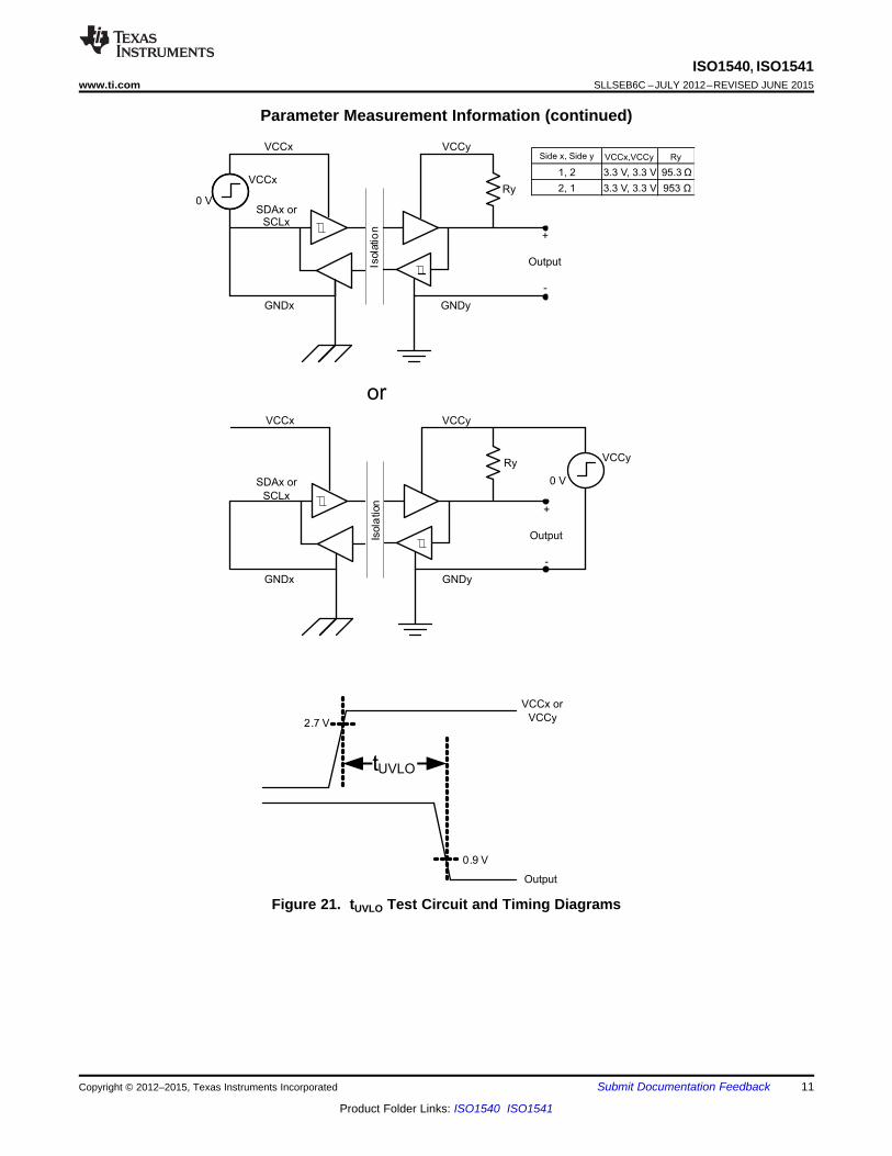
Parameter Measurement Information (continued)
Figure 21. tUVLO Test Circuit and Timing Diagrams
Copyright © 2012–2015, Texas Instruments Incorporated Submit Documentation Feedback 11
Product Folder Links: ISO1540 ISO1541
SDA2
SCL1 SCL2
GND2GND1
VCC2VCC1
SDA1
VREF
VREF
Iso
lati
on
Ca
pa
cito
r
ISO1540, ISO1541SLLSEB6C –JULY 2012–REVISED JUNE 2015 www.ti.com
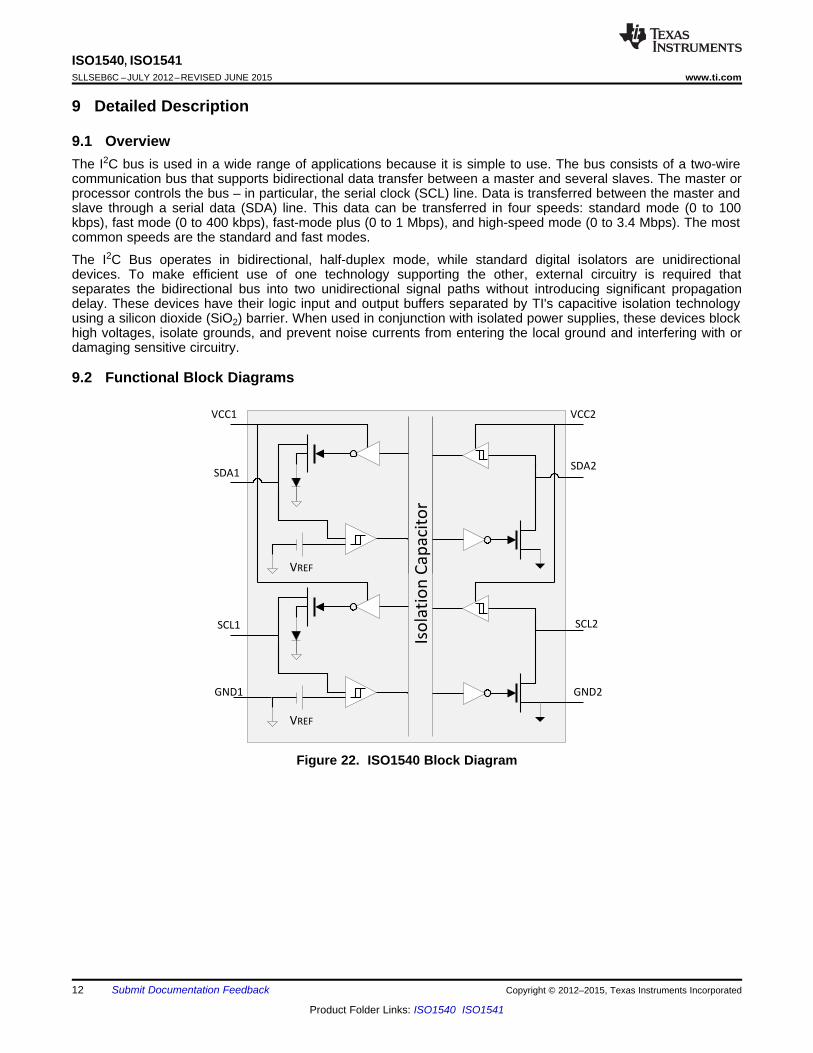
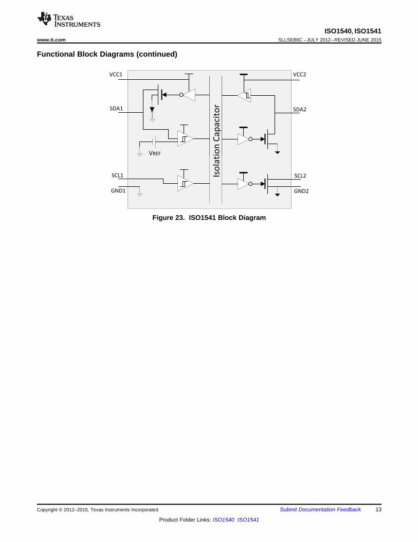
9 Detailed Description
9.1 OverviewThe I2C bus is used in a wide range of applications because it is simple to use. The bus consists of a two-wirecommunication bus that supports bidirectional data transfer between a master and several slaves. The master orprocessor controls the bus – in particular, the serial clock (SCL) line. Data is transferred between the master andslave through a serial data (SDA) line. This data can be transferred in four speeds: standard mode (0 to 100kbps), fast mode (0 to 400 kbps), fast-mode plus (0 to 1 Mbps), and high-speed mode (0 to 3.4 Mbps). The mostcommon speeds are the standard and fast modes.
The I2C Bus operates in bidirectional, half-duplex mode, while standard digital isolators are unidirectionaldevices. To make efficient use of one technology supporting the other, external circuitry is required thatseparates the bidirectional bus into two unidirectional signal paths without introducing significant propagationdelay. These devices have their logic input and output buffers separated by TI's capacitive isolation technologyusing a silicon dioxide (SiO2) barrier. When used in conjunction with isolated power supplies, these devices blockhigh voltages, isolate grounds, and prevent noise currents from entering the local ground and interfering with ordamaging sensitive circuitry.
9.2 Functional Block Diagrams
Figure 22. ISO1540 Block Diagram
12 Submit Documentation Feedback Copyright © 2012–2015, Texas Instruments Incorporated
Product Folder Links: ISO1540 ISO1541
SDA2
SCL1 SCL2
GND2GND1
VCC2VCC1
SDA1
VREF
Iso
lati
on
Ca
pa
cito
r
ISO1540, ISO1541www.ti.com SLLSEB6C –JULY 2012–REVISED JUNE 2015
Functional Block Diagrams (continued)
Figure 23. ISO1541 Block Diagram
Copyright © 2012–2015, Texas Instruments Incorporated Submit Documentation Feedback 13
Product Folder Links: ISO1540 ISO1541
ISO1540, ISO1541SLLSEB6C –JULY 2012–REVISED JUNE 2015 www.ti.com
9.3 Feature DescriptionThe ISO device enables a complete isolated I²C interface to be implemented within a small form factor havingfollowing features:
Table 1. Features ListFEATURES DESCRIPTION ISO1540 ISO1541
UL 1577 Isolation Voltage (Single) (Vrms) 2500 2500DIN V VDE V 0884-10 (VDE V 0884-10):2006-12 Transient Overvoltage Rating 4242 4242(Vpk)DIN V VDE V 0884-10 (VDE V 0884-10):2006-12 Working Voltage Rating (Vpk) 566 566CSA Isolation Rating (Vrms) 2800 2800CSA 60950-1 Basic Working (Vrms) 390 390CSA 61010-1 Basic Working (Vrms) 300 300CSA 61010-1 Reinforced Working (Vrms) 150 150Data Rate (Mbps) 1 1Number of Channels 2 2Serial Clock Bidirectional UnidirectionalSerial Data Bidirectional BidirectionalOperating Temperature (°C) –40 to 125 –40 to 125Pin/Package SOIC (8) SOIC (8)
9.3.1 Insulation and Safety-Related Specification for D-8 Packageover recommended operating conditions, unless otherwise noted
PARAMETER TEST CONDITIONS MIN TYP MAX UNITShortest terminal-to-terminal distanceL(I01) Minimum air gap (Clearance) 4.8 mmthrough air
Minimum external tracking Shortest terminal-to-terminal distanceL(I02) 4.3 mm(Creepage) across the package surfaceTracking resistance (comparativeCTI DIN IEC 60112 / VDE 0303 Part 1 >400 Vtracking index)Minimum internal gap (internal Distance through the insulation 0.014 mmclearance)
VIO = 500 V, TA = 25°C >1012 ΩIsolation resistance, input toRIO output (1) VIO = 500 V, 100°C ≤ TA ≤ TA max >1011 ΩBarrier capacitance, input toCIO VIO = 0.4 x sin(2E6πt) 1 pFoutput (1)
CI Input capacitance (2) See Electrical Characteristics pF
(1) All pins on each side of the barrier tied together creating a 2-terminal device.(2) Measured from input pin to ground.
space
NOTECreepage and clearance requirements should be applied according to the specificapplication isolation standards. Care should be taken to maintain these distances on aboard design to ensure that the mounting pads for the isolator do not reduce this distance.
Creepage and clearance on the printed-circuit-board (PCB) become equal in certaincases. Techniques such as inserting grooves and/or ribs on the PCB are used to helpincrease these specifications.
14 Submit Documentation Feedback Copyright © 2012–2015, Texas Instruments Incorporated
Product Folder Links: ISO1540 ISO1541
ISO1540, ISO1541www.ti.com SLLSEB6C –JULY 2012–REVISED JUNE 2015
9.3.2 DIN V VDE V 0884-10 (VDE V 0884-10):2006-12 Insulation Characteristics (3)
over recommended operating conditions, unless otherwise noted
PARAMETER TEST CONDITIONS SPECIFICATION UNITMaximum working insulationVIORM 566 VPEAKvoltage
Method a, After environmental tests subgroup 1,VPR = VIORM × 1.6, t = 10 s, 906Partial Discharge < 5 pCMethod b1, After environmental tests subgroup 1,
VPR Input-to-Output test voltage VPR = VIORM × 1.875, t = 1 s (100% production), 1062 VPEAKPartial Discharge < 5 pCAfter Input/Output safety test subgroup 2/3,VPR = VIORM × 1.2, t = 10 s, 680Partial Discharge < 5 pCVTEST = VOITM
VIOTM Transient overvoltage t = 60 s (qualification) 4242 VPEAKt = 1 s (100% production)
RS Insulation resistance VIO = 500 V at TS >109 ΩPollution degree 2
(3) Climatic Classification 40/125/21
9.3.3 IEC 60664-1 Ratings Table
PARAMETER TEST CONDITIONS SPECIFICATIONBasic isolation group Material group II
Rated mains voltage ≤ 150 VRMS I–IVInstallation classification Rated mains voltage ≤ 300 VRMS I–III
Rated mains voltage ≤ 400 VRMS I–II
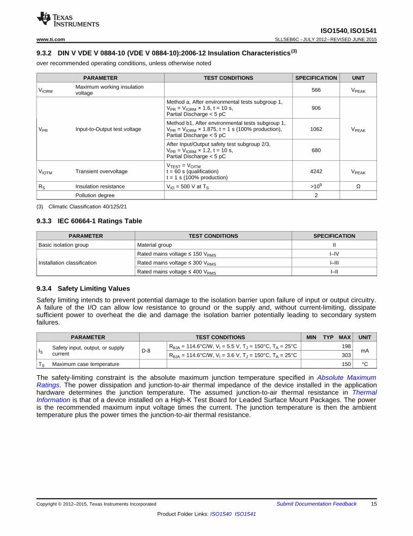
9.3.4 Safety Limiting ValuesSafety limiting intends to prevent potential damage to the isolation barrier upon failure of input or output circuitry.A failure of the I/O can allow low resistance to ground or the supply and, without current-limiting, dissipatesufficient power to overheat the die and damage the isolation barrier potentially leading to secondary systemfailures.
PARAMETER TEST CONDITIONS MIN TYP MAX UNITRθJA = 114.6°C/W, VI = 5.5 V, TJ = 150°C, TA = 25°C 198Safety input, output, or supplyIS D-8 mAcurrent RθJA = 114.6°C/W, VI = 3.6 V, TJ = 150°C, TA = 25°C 303
TS Maximum case temperature 150 °C
The safety-limiting constraint is the absolute maximum junction temperature specified in Absolute MaximumRatings. The power dissipation and junction-to-air thermal impedance of the device installed in the applicationhardware determines the junction temperature. The assumed junction-to-air thermal resistance in ThermalInformation is that of a device installed on a High-K Test Board for Leaded Surface Mount Packages. The poweris the recommended maximum input voltage times the current. The junction temperature is then the ambienttemperature plus the power times the junction-to-air thermal resistance.
Copyright © 2012–2015, Texas Instruments Incorporated Submit Documentation Feedback 15
Product Folder Links: ISO1540 ISO1541
0
300
0 50 100 150 200
Safe
ty L
imit
ing
Cu
rren
t (m
A)
Case Temperature ( C)o
200
350
100
250
150
50
VCC1 = = 3.6 VVCC2
VCC1 = = 5.5 VVCC2
ISO1540, ISO1541SLLSEB6C –JULY 2012–REVISED JUNE 2015 www.ti.com
Figure 24. ISO154x Thermal Derating Curve
9.3.5 Regulatory Information
VDE CSA UL CQCCertified according to DIN V Certified according to CSA Recognized under UL 1577VDE V 0884-10 (VDE V 0884- Component Acceptance Notice 5A, Certified according to GB4943.1-Component Recognition10):2006-12 and DIN EN CSA/IEC 60950-1 and CSA/IEC 2011Program61010-1 61010-1
Basic insulation per CSA 60950-1-07and IEC 60950-1 (2nd Ed), 390 VRMS
Basic Insulation maximum working voltageMaximum Transient Basic insulation per CSA 61010-1-04 Basic Insulation, Altitude ≤ 5000Single Protection IsolationOvervoltage, 4242 VPK and IEC 61010-1 (2nd Ed), 300 VRMS m, Tropical Climate, 250 VRMSVoltage, 2500 VRMS
(1)Maximum Working Voltage, maximum working voltage maximum working voltage566 VPK Reinforced insulation per CSA 61010-
1-04 and IEC 61010-1 (2nd Ed), 150VRMS maximum working voltage
Certificate number :Certificate number: 40016131 Master contract number: 220991 File number: E181974 CQC14001109540
(1) Production tested ≥ 3000 VRMS for 1 second in accordance with UL 1577.
9.4 Device Functional ModesISO154x functional modes are shown in Table 2.
Table 2. Function Table (1)
POWER STATE INPUT OUTPUTVCC1 or VCC2 < 2.1 V X Z
VCC1 and VCC2 > 2.8 V L LVCC1 and VCC2 > 2.8 V H ZVCC1 and VCC2 > 2.8 V Z (2) ?
(1) H = High Level; L = Low Level; Z = High Impedance or Float; X = Irrelevant; ? = Indeterminate(2) Invalid input condition as an I2C system requires that a pullup resistor to VCC is connected.
16 Submit Documentation Feedback Copyright © 2012–2015, Texas Instruments Incorporated
Product Folder Links: ISO1540 ISO1541
GND
ADC
Slave
GND
DAC
Slave
GND
μC
Slave
GND
μC
Master
SDA SCL SDA SCL SDA SCLSDA SCL
SDA
SCL
VDD
RPURPU RPURPU RPURPURPURPU
ISO1540, ISO1541www.ti.com SLLSEB6C –JULY 2012–REVISED JUNE 2015
10 Application and Implementation
NOTEInformation in the following applications sections is not part of the TI componentspecification, and TI does not warrant its accuracy or completeness. TI’s customers areresponsible for determining suitability of components for their purposes. Customers shouldvalidate and test their design implementation to confirm system functionality.
10.1 Application Information
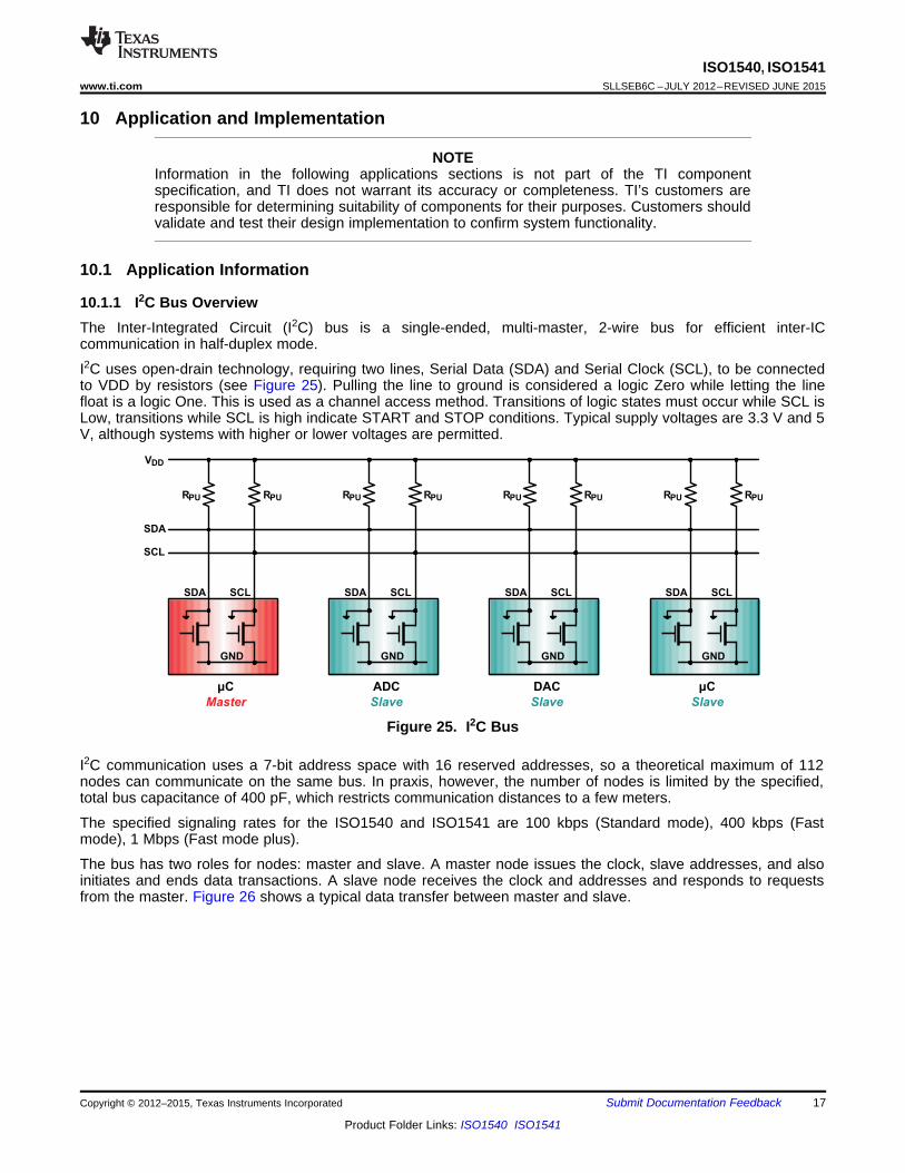
10.1.1 I2C Bus OverviewThe Inter-Integrated Circuit (I2C) bus is a single-ended, multi-master, 2-wire bus for efficient inter-ICcommunication in half-duplex mode.
I2C uses open-drain technology, requiring two lines, Serial Data (SDA) and Serial Clock (SCL), to be connectedto VDD by resistors (see Figure 25). Pulling the line to ground is considered a logic Zero while letting the linefloat is a logic One. This is used as a channel access method. Transitions of logic states must occur while SCL isLow, transitions while SCL is high indicate START and STOP conditions. Typical supply voltages are 3.3 V and 5V, although systems with higher or lower voltages are permitted.
Figure 25. I2C Bus
I2C communication uses a 7-bit address space with 16 reserved addresses, so a theoretical maximum of 112nodes can communicate on the same bus. In praxis, however, the number of nodes is limited by the specified,total bus capacitance of 400 pF, which restricts communication distances to a few meters.
The specified signaling rates for the ISO1540 and ISO1541 are 100 kbps (Standard mode), 400 kbps (Fastmode), 1 Mbps (Fast mode plus).
The bus has two roles for nodes: master and slave. A master node issues the clock, slave addresses, and alsoinitiates and ends data transactions. A slave node receives the clock and addresses and responds to requestsfrom the master. Figure 26 shows a typical data transfer between master and slave.
Copyright © 2012–2015, Texas Instruments Incorporated Submit Documentation Feedback 17
Product Folder Links: ISO1540 ISO1541
From Master to Slave
From Slave to Master
S Slave Address R A DATA A DATA A P
S Slave Address W A DATA A DATA A P
Master Transmitter writing to Slave Receiver
Master Receiver reading from Slave Transmitter
A = acknowledge
A = not acknowledge
S = Start
P = Stop
R = Read
W = Write
1 - 7 1 - 88 9 9 1 - 8 9
SDA
SCL
S P
START
Condition
STOP
condition
7-bit
ADDRESS
8-bit
DATA
8-bit
DATAR/W
ACK /
NACKACK ACK
ISO1540, ISO1541SLLSEB6C –JULY 2012–REVISED JUNE 2015 www.ti.com
Application Information (continued)
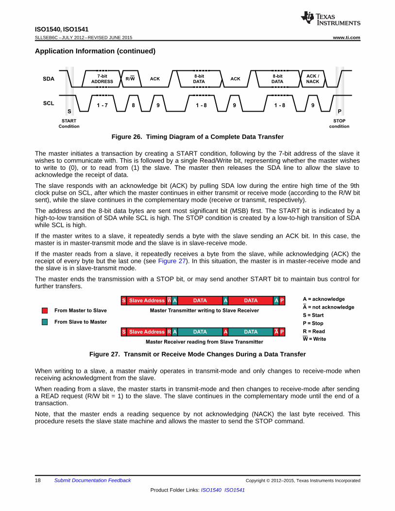
Figure 26. Timing Diagram of a Complete Data Transfer
The master initiates a transaction by creating a START condition, following by the 7-bit address of the slave itwishes to communicate with. This is followed by a single Read/Write bit, representing whether the master wishesto write to (0), or to read from (1) the slave. The master then releases the SDA line to allow the slave toacknowledge the receipt of data.
The slave responds with an acknowledge bit (ACK) by pulling SDA low during the entire high time of the 9thclock pulse on SCL, after which the master continues in either transmit or receive mode (according to the R/W bitsent), while the slave continues in the complementary mode (receive or transmit, respectively).
The address and the 8-bit data bytes are sent most significant bit (MSB) first. The START bit is indicated by ahigh-to-low transition of SDA while SCL is high. The STOP condition is created by a low-to-high transition of SDAwhile SCL is high.
If the master writes to a slave, it repeatedly sends a byte with the slave sending an ACK bit. In this case, themaster is in master-transmit mode and the slave is in slave-receive mode.
If the master reads from a slave, it repeatedly receives a byte from the slave, while acknowledging (ACK) thereceipt of every byte but the last one (see Figure 27). In this situation, the master is in master-receive mode andthe slave is in slave-transmit mode.
The master ends the transmission with a STOP bit, or may send another START bit to maintain bus control forfurther transfers.
Figure 27. Transmit or Receive Mode Changes During a Data Transfer
When writing to a slave, a master mainly operates in transmit-mode and only changes to receive-mode whenreceiving acknowledgment from the slave.
When reading from a slave, the master starts in transmit-mode and then changes to receive-mode after sendinga READ request (R/W bit = 1) to the slave. The slave continues in the complementary mode until the end of atransaction.
Note, that the master ends a reading sequence by not acknowledging (NACK) the last byte received. Thisprocedure resets the slave state machine and allows the master to send the STOP command.
18 Submit Documentation Feedback Copyright © 2012–2015, Texas Instruments Incorporated
Product Folder Links: ISO1540 ISO1541
VOL1
VIHT1
SDA1
SDA2
SDA2
SDA1
transmit
delay
transmitdelay
receivedelay
VIHT2
50%
50%
30%
30%
receivedelay
receive
delay
VCC1VCC1VCC2VCC2
VCC1 VCC1 VCC2 VCC2
VSDA1
VC-out
VILT1 VIHT1 VOL1
40mV
RPU1 RPU2
VCC1 VCC2
SDA1
GND1GND2
SDA2
VREF
A
B
D
C
ISO1540
50mVCbusCnode
ISO1540, ISO1541www.ti.com SLLSEB6C –JULY 2012–REVISED JUNE 2015
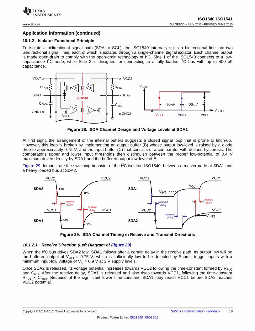
Application Information (continued)10.1.2 Isolator Functional PrincipleTo isolate a bidirectional signal path (SDA or SCL), the ISO1540 internally splits a bidirectional line into twounidirectional signal lines, each of which is isolated through a single-channel digital isolator. Each channel outputis made open-drain to comply with the open-drain technology of I2C. Side 1 of the ISO1540 connects to a low-capacitance I2C node, while Side 2 is designed for connecting to a fully loaded I2C bus with up to 400 pFcapacitance.
Figure 28. SDA Channel Design and Voltage Levels at SDA1
At first sight, the arrangement of the internal buffers suggests a closed signal loop that is prone to latch-up.However, this loop is broken by implementing an output buffer (B) whose output low-level is raised by a diodedrop to approximately 0.75 V, and the input buffer (C) that consists of a comparator with defined hysteresis. Thecomparator’s upper and lower input thresholds then distinguish between the proper low-potential of 0.4 Vmaximum driven directly by SDA1 and the buffered output low-level of B.
Figure 29 demonstrate the switching behavior of the I2C isolator, ISO1540, between a master node at SDA1 anda heavy loaded bus at SDA2.
Figure 29. SDA Channel Timing in Receive and Transmit Directions
10.1.2.1 Receive Direction (Left Diagram of Figure 29)When the I2C bus drives SDA2 low, SDA1 follows after a certain delay in the receive path. Its output low will bethe buffered output of VOL1 = 0.75 V, which is sufficiently low to be detected by Schmitt-trigger inputs with aminimum input-low voltage of VIL = 0.9 V at 3 V supply levels.
Once SDA2 is released, its voltage potential increases towards VCC2 following the time-constant formed by RPU2and Cbus. After the receive delay, SDA1 is released and also rises towards VCC1, following the time-constantRPU1 × Cnode. Because of the significant lower time-constant, SDA1 may reach VCC1 before SDA2 reachesVCC2 potential.
Copyright © 2012–2015, Texas Instruments Incorporated Submit Documentation Feedback 19
Product Folder Links: ISO1540 ISO1541
VCC1 VCC2
GND1 GND2
8
7
4 54
XOUT
XIN
5
6
2
MSP430
G2132
1
2
3 ISO1541
DVss
DVcc
0.1μF0.1μF 0.1μF
6SDA
SCL
9
8
10μF
VS
0.1μF
MBR0520L
MBR0520L
1:2.2
0.1μF
3
1
D2
SN6501
D1
Vcc
4,5
2
GND
3.3V
IN
ON GND
OUT1 5
23LP2981-50 10μF
10μF
SDA2SDA1
SCL1 SCL2
1.5k 1.5k 1.5k 1.5k
0.1μF
8
VDD
GND
AIN0
2
1
9
10SDA
SCL
4
ADDR
ADS1115
AIN3RDY
3
4 Analog
Inputs
7
VIN
GND
VOUT26
4REF5040
1μF22μF0.1μF
4
VDD
VOUTA11
10SDA
SCL
1
DAC8574
VOUTD8GND
6
12 3
VREFHA2
15
IOVDD
VREFL
5
4 Analog
Outputs
A3
16
A0
13
9
14LDAC
A1
5VISO
5VISO
5VISO
5VISO
SD
A
SC
LISO-BARRIER
1Ω
ISO1540, ISO1541SLLSEB6C –JULY 2012–REVISED JUNE 2015 www.ti.com
Application Information (continued)10.1.2.2 Transmit Direction (Right Diagram of Figure 29)When a master drives SDA1 low, SDA2 follows after a certain delay in the transmit direction. When SDA2 turnslow it also causes the output of buffer B to turn low but at a higher 0.75 V level. This level cannot be observedimmediately as it is overwritten by the master’s lower low-level.
However, when the master releases SDA1, its voltage potential increases and first must pass the upper inputthreshold of the comparator, VIHT1, to release SDA2. SDA1 then increases further until it reaches the bufferedoutput level of VOL1 = 0.75 V, maintained by the receive path. Once comparator C turns high, SDA2 is releasedafter the delay in transmit direction. It takes another receive delay until B’s output turns high and fully releasesSDA1 to move toward VCC1 potential.
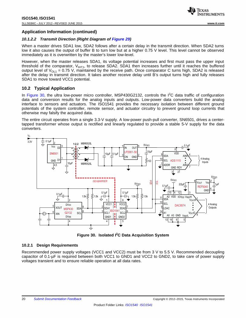
10.2 Typical ApplicationIn Figure 30, the ultra low-power micro controller, MSP430G2132, controls the I2C data traffic of configurationdata and conversion results for the analog inputs and outputs. Low-power data converters build the analoginterface to sensors and actuators. The ISO1541 provides the necessary isolation between different groundpotentials of the system controller, remote sensor, and actuator circuitry to prevent ground loop currents thatotherwise may falsify the acquired data.
The entire circuit operates from a single 3.3-V supply. A low-power push-pull converter, SN6501, drives a center-tapped transformer whose output is rectified and linearly regulated to provide a stable 5-V supply for the dataconverters.
Figure 30. Isolated I2C Data Acquisition System
10.2.1 Design RequirementsRecommended power supply voltages (VCC1 and VCC2) must be from 3 V to 5.5 V. Recommended decouplingcapacitor of 0.1-µF is required between both VCC1 to GND1 and VCC2 to GND2, to take care of power supplyvoltages transient and to ensure reliable operation at all data rates.
20 Submit Documentation Feedback Copyright © 2012–2015, Texas Instruments Incorporated
Product Folder Links: ISO1540 ISO1541
ISO1541
SCL1
SDA1
GND2GND1
VCC2VCC1
Iso
lati
on
Ca
pa
cito
r
8
7
6
54
3
2
1
Side 1 Side 2
0.1PF
1k:1k: 1k:0.1PF
1k:
2mm max 2mm max
SDA2
SCL2
ISO1540
SDA2
SCL2SCL1
GND2GND1
VCC2VCC1
SDA1
`Iso
lati
on
Ca
pa
cito
r
8
7
6
54
3
2
1
Side 1 Side 2
0.1PF1k:1k: 1k:
0.1PF1k:
2mm max 2mm max
ISO1540, ISO1541www.ti.com SLLSEB6C –JULY 2012–REVISED JUNE 2015
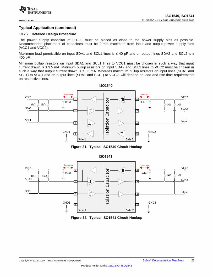
Typical Application (continued)10.2.2 Detailed Design ProcedureThe power supply capacitor of 0.1-µF must be placed as close to the power supply pins as possible.Recommended placement of capacitors must be 2-mm maximum from input and output power supply pins(VCC1 and VCC2).
Maximum load permissible on input SDA1 and SCL1 lines is ≤ 40 pF and on output lines SDA2 and SCL2 is ≤400 pF.
Minimum pullup resistors on input SDA1 and SCL1 lines to VCC1 must be chosen in such a way that inputcurrent drawn is ≤ 3.5 mA. Minimum pullup resistors on input SDA2 and SCL2 lines to VCC2 must be chosen insuch a way that output current drawn is ≤ 35 mA. Whereas maximum pullup resistors on input lines (SDA1 andSCL1) to VCC1 and on output lines (SDA1 and SCL1) to VCC2, will depend on load and rise time requirementson respective lines.
Figure 31. Typical ISO1540 Circuit Hookup
Figure 32. Typical ISO1541 Circuit Hookup
Copyright © 2012–2015, Texas Instruments Incorporated Submit Documentation Feedback 21
Product Folder Links: ISO1540 ISO1541
T = 25 C
VCC1 = 3.6 V
A
o
Time - 50 ns/div
500 m
V/d
iv
900 mV
VOL1
GND1
ISO1540, ISO1541SLLSEB6C –JULY 2012–REVISED JUNE 2015 www.ti.com
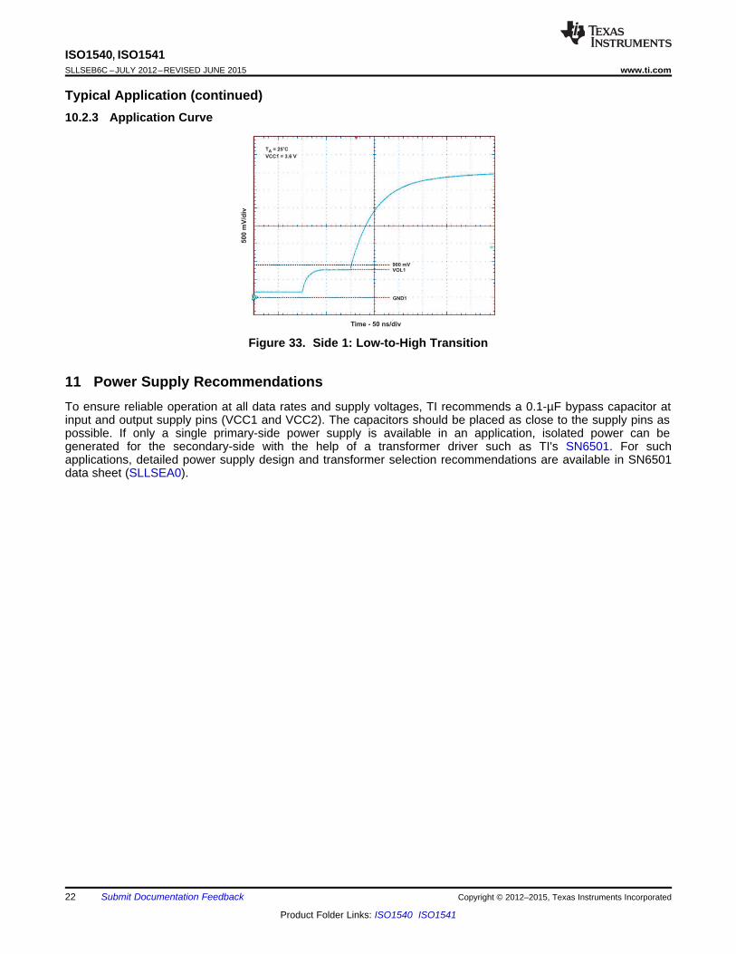
Typical Application (continued)10.2.3 Application Curve
Figure 33. Side 1: Low-to-High Transition
11 Power Supply RecommendationsTo ensure reliable operation at all data rates and supply voltages, TI recommends a 0.1-µF bypass capacitor atinput and output supply pins (VCC1 and VCC2). The capacitors should be placed as close to the supply pins aspossible. If only a single primary-side power supply is available in an application, isolated power can begenerated for the secondary-side with the help of a transformer driver such as TI's SN6501. For suchapplications, detailed power supply design and transformer selection recommendations are available in SN6501data sheet (SLLSEA0).
22 Submit Documentation Feedback Copyright © 2012–2015, Texas Instruments Incorporated
Product Folder Links: ISO1540 ISO1541
10 mils
10 mils
40 milsFR-4
0r ~ 4.5
Keep this space free
from planes,traces , pads,
and vias
Ground plane
Power plane
Low-speed traces
High-speed traces
ISO1540, ISO1541www.ti.com SLLSEB6C –JULY 2012–REVISED JUNE 2015
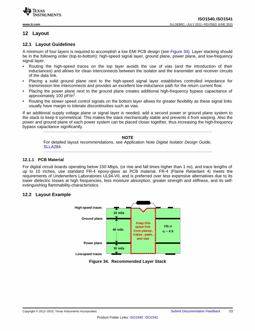
12 Layout
12.1 Layout GuidelinesA minimum of four layers is required to accomplish a low EMI PCB design (see Figure 34). Layer stacking shouldbe in the following order (top-to-bottom): high-speed signal layer, ground plane, power plane, and low-frequencysignal layer.• Routing the high-speed traces on the top layer avoids the use of vias (and the introduction of their
inductances) and allows for clean interconnects between the isolator and the transmitter and receiver circuitsof the data link.
• Placing a solid ground plane next to the high-speed signal layer establishes controlled impedance fortransmission line interconnects and provides an excellent low-inductance path for the return current flow.
• Placing the power plane next to the ground plane creates additional high-frequency bypass capacitance ofapproximately 100 pF/in2.
• Routing the slower speed control signals on the bottom layer allows for greater flexibility as these signal linksusually have margin to tolerate discontinuities such as vias.
If an additional supply voltage plane or signal layer is needed, add a second power or ground plane system tothe stack to keep it symmetrical. This makes the stack mechanically stable and prevents it from warping. Also thepower and ground plane of each power system can be placed closer together, thus increasing the high-frequencybypass capacitance significantly.
NOTEFor detailed layout recommendations, see Application Note Digital Isolator Design Guide,SLLA284.
12.1.1 PCB MaterialFor digital circuit boards operating below 150 Mbps, (or rise and fall times higher than 1 ns), and trace lengths ofup to 10 inches, use standard FR-4 epoxy-glass as PCB material. FR-4 (Flame Retardant 4) meets therequirements of Underwriters Laboratories UL94-V0, and is preferred over less expensive alternatives due to itslower dielectric losses at high frequencies, less moisture absorption, greater strength and stiffness, and its self-extinguishing flammability-characteristics.
12.2 Layout Example
Figure 34. Recommended Layer Stack
Copyright © 2012–2015, Texas Instruments Incorporated Submit Documentation Feedback 23
Product Folder Links: ISO1540 ISO1541
ISO1540, ISO1541SLLSEB6C –JULY 2012–REVISED JUNE 2015 www.ti.com
13 Device and Documentation Support
13.1 Documentation Support
13.1.1 Related DocumentationFor related documentation see the following:• SLLSEA0, Transformer Driver for Isolated Power Supplies• SLLA284, Digital Isolator Design Guide• SLLA353, TI Isolation Glossary
13.2 Related LinksThe table below lists quick access links. Categories include technical documents, support and communityresources, tools and software, and quick access to sample or buy.
Table 3. Related LinksTECHNICAL TOOLS & SUPPORT &PARTS PRODUCT FOLDER SAMPLE & BUY DOCUMENTS SOFTWARE COMMUNITY
ISO1540 Click here Click here Click here Click here Click hereISO1541 Click here Click here Click here Click here Click here
13.3 Community ResourcesThe following links connect to TI community resources. Linked contents are provided "AS IS" by the respectivecontributors. They do not constitute TI specifications and do not necessarily reflect TI's views; see TI's Terms ofUse.
TI E2E™ Online Community TI's Engineer-to-Engineer (E2E) Community. Created to foster collaborationamong engineers. At e2e.ti.com, you can ask questions, share knowledge, explore ideas and helpsolve problems with fellow engineers.
Design Support TI's Design Support Quickly find helpful E2E forums along with design support tools andcontact information for technical support.
13.4 TrademarksE2E is a trademark of Texas Instruments.All other trademarks are the property of their respective owners.
13.5 Electrostatic Discharge CautionThese devices have limited built-in ESD protection. The leads should be shorted together or the device placed in conductive foamduring storage or handling to prevent electrostatic damage to the MOS gates.
13.6 GlossarySLYZ022 — TI Glossary.
This glossary lists and explains terms, acronyms, and definitions.
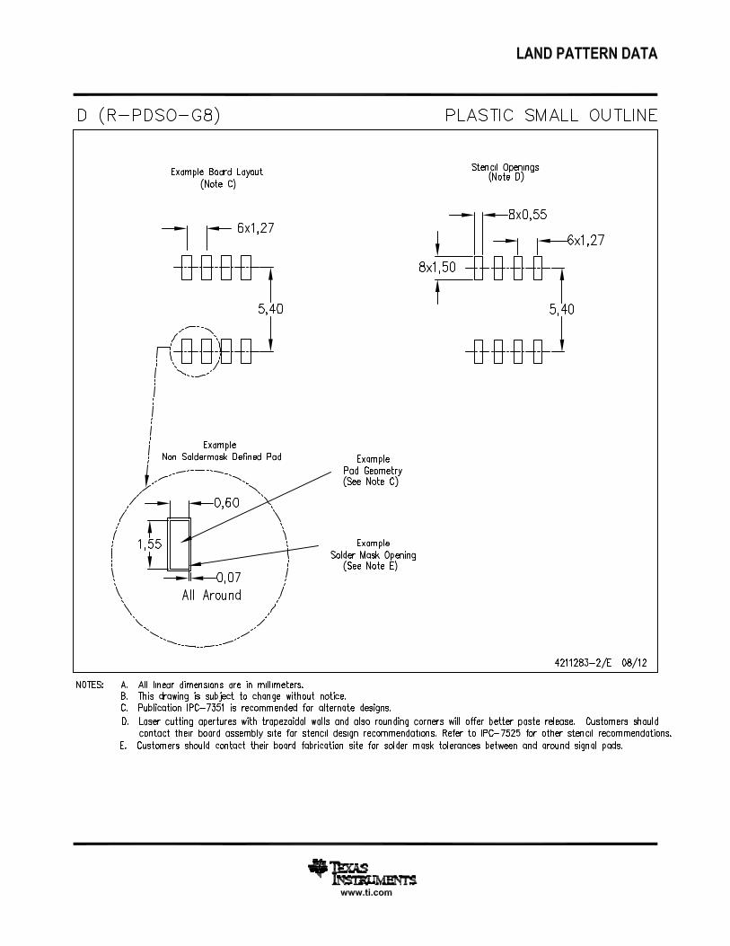
14 Mechanical, Packaging, and Orderable InformationThe following pages include mechanical, packaging, and orderable information. This information is the mostcurrent data available for the designated devices. This data is subject to change without notice and revision ofthis document. For browser-based versions of this data sheet, refer to the left-hand navigation.
24 Submit Documentation Feedback Copyright © 2012–2015, Texas Instruments Incorporated
Product Folder Links: ISO1540 ISO1541
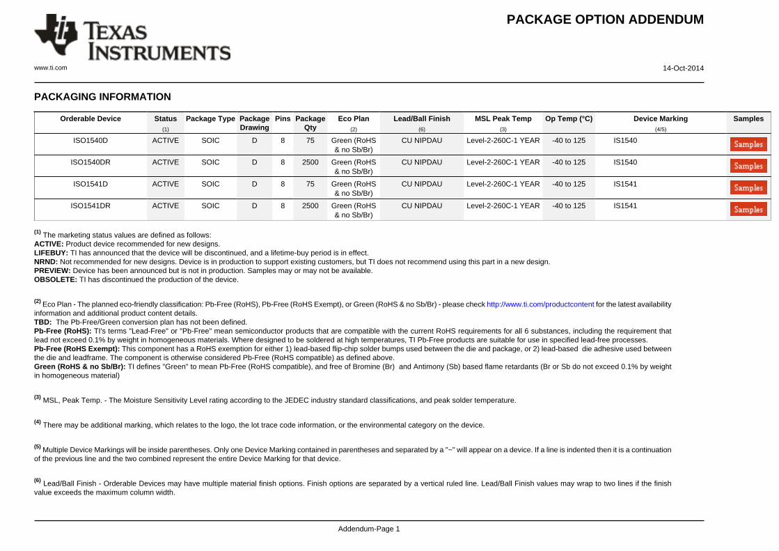
PACKAGE OPTION ADDENDUM
www.ti.com 14-Oct-2014
Addendum-Page 1
PACKAGING INFORMATION
Orderable Device Status(1)
Package Type PackageDrawing
Pins PackageQty
Eco Plan(2)
Lead/Ball Finish(6)
MSL Peak Temp(3)
Op Temp (°C) Device Marking(4/5)
Samples
ISO1540D ACTIVE SOIC D 8 75 Green (RoHS& no Sb/Br)
CU NIPDAU Level-2-260C-1 YEAR -40 to 125 IS1540
ISO1540DR ACTIVE SOIC D 8 2500 Green (RoHS& no Sb/Br)
CU NIPDAU Level-2-260C-1 YEAR -40 to 125 IS1540
ISO1541D ACTIVE SOIC D 8 75 Green (RoHS& no Sb/Br)
CU NIPDAU Level-2-260C-1 YEAR -40 to 125 IS1541
ISO1541DR ACTIVE SOIC D 8 2500 Green (RoHS& no Sb/Br)
CU NIPDAU Level-2-260C-1 YEAR -40 to 125 IS1541
(1) The marketing status values are defined as follows:ACTIVE: Product device recommended for new designs.LIFEBUY: TI has announced that the device will be discontinued, and a lifetime-buy period is in effect.NRND: Not recommended for new designs. Device is in production to support existing customers, but TI does not recommend using this part in a new design.PREVIEW: Device has been announced but is not in production. Samples may or may not be available.OBSOLETE: TI has discontinued the production of the device.
(2) Eco Plan - The planned eco-friendly classification: Pb-Free (RoHS), Pb-Free (RoHS Exempt), or Green (RoHS & no Sb/Br) - please check http://www.ti.com/productcontent for the latest availabilityinformation and additional product content details.TBD: The Pb-Free/Green conversion plan has not been defined.Pb-Free (RoHS): TI's terms "Lead-Free" or "Pb-Free" mean semiconductor products that are compatible with the current RoHS requirements for all 6 substances, including the requirement thatlead not exceed 0.1% by weight in homogeneous materials. Where designed to be soldered at high temperatures, TI Pb-Free products are suitable for use in specified lead-free processes.Pb-Free (RoHS Exempt): This component has a RoHS exemption for either 1) lead-based flip-chip solder bumps used between the die and package, or 2) lead-based die adhesive used betweenthe die and leadframe. The component is otherwise considered Pb-Free (RoHS compatible) as defined above.Green (RoHS & no Sb/Br): TI defines "Green" to mean Pb-Free (RoHS compatible), and free of Bromine (Br) and Antimony (Sb) based flame retardants (Br or Sb do not exceed 0.1% by weightin homogeneous material)
(3) MSL, Peak Temp. - The Moisture Sensitivity Level rating according to the JEDEC industry standard classifications, and peak solder temperature.
(4) There may be additional marking, which relates to the logo, the lot trace code information, or the environmental category on the device.
(5) Multiple Device Markings will be inside parentheses. Only one Device Marking contained in parentheses and separated by a "~" will appear on a device. If a line is indented then it is a continuationof the previous line and the two combined represent the entire Device Marking for that device.
(6) Lead/Ball Finish - Orderable Devices may have multiple material finish options. Finish options are separated by a vertical ruled line. Lead/Ball Finish values may wrap to two lines if the finishvalue exceeds the maximum column width.
PACKAGE OPTION ADDENDUM
www.ti.com 14-Oct-2014
Addendum-Page 2
Important Information and Disclaimer:The information provided on this page represents TI's knowledge and belief as of the date that it is provided. TI bases its knowledge and belief on informationprovided by third parties, and makes no representation or warranty as to the accuracy of such information. Efforts are underway to better integrate information from third parties. TI has taken andcontinues to take reasonable steps to provide representative and accurate information but may not have conducted destructive testing or chemical analysis on incoming materials and chemicals.TI and TI suppliers consider certain information to be proprietary, and thus CAS numbers and other limited information may not be available for release.
In no event shall TI's liability arising out of such information exceed the total purchase price of the TI part(s) at issue in this document sold by TI to Customer on an annual basis.
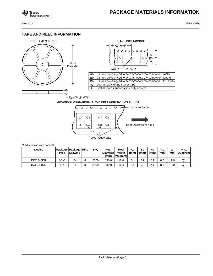
TAPE AND REEL INFORMATION
*All dimensions are nominal
Device PackageType
PackageDrawing
Pins SPQ ReelDiameter
(mm)
ReelWidth
W1 (mm)
A0(mm)
B0(mm)
K0(mm)
P1(mm)
W(mm)
Pin1Quadrant
ISO1540DR SOIC D 8 2500 330.0 12.4 6.4 5.2 2.1 8.0 12.0 Q1
ISO1541DR SOIC D 8 2500 330.0 12.4 6.4 5.2 2.1 8.0 12.0 Q1
PACKAGE MATERIALS INFORMATION
www.ti.com 13-Feb-2016
Pack Materials-Page 1
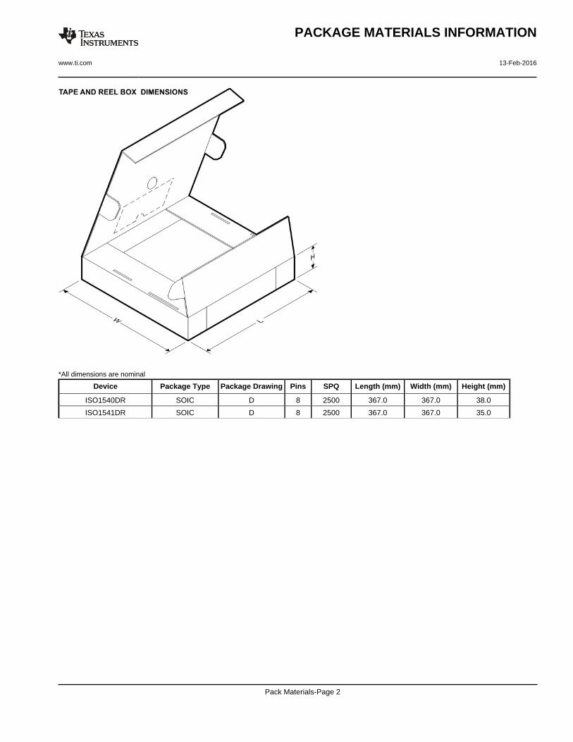
*All dimensions are nominal
Device Package Type Package Drawing Pins SPQ Length (mm) Width (mm) Height (mm)
ISO1540DR SOIC D 8 2500 367.0 367.0 38.0
ISO1541DR SOIC D 8 2500 367.0 367.0 35.0
PACKAGE MATERIALS INFORMATION
www.ti.com 13-Feb-2016
Pack Materials-Page 2
IMPORTANT NOTICE
Texas Instruments Incorporated and its subsidiaries (TI) reserve the right to make corrections, enhancements, improvements and otherchanges to its semiconductor products and services per JESD46, latest issue, and to discontinue any product or service per JESD48, latestissue. Buyers should obtain the latest relevant information before placing orders and should verify that such information is current andcomplete. All semiconductor products (also referred to herein as “components”) are sold subject to TI’s terms and conditions of salesupplied at the time of order acknowledgment.TI warrants performance of its components to the specifications applicable at the time of sale, in accordance with the warranty in TI’s termsand conditions of sale of semiconductor products. Testing and other quality control techniques are used to the extent TI deems necessaryto support this warranty. Except where mandated by applicable law, testing of all parameters of each component is not necessarilyperformed.TI assumes no liability for applications assistance or the design of Buyers’ products. Buyers are responsible for their products andapplications using TI components. To minimize the risks associated with Buyers’ products and applications, Buyers should provideadequate design and operating safeguards.TI does not warrant or represent that any license, either express or implied, is granted under any patent right, copyright, mask work right, orother intellectual property right relating to any combination, machine, or process in which TI components or services are used. Informationpublished by TI regarding third-party products or services does not constitute a license to use such products or services or a warranty orendorsement thereof. Use of such information may require a license from a third party under the patents or other intellectual property of thethird party, or a license from TI under the patents or other intellectual property of TI.Reproduction of significant portions of TI information in TI data books or data sheets is permissible only if reproduction is without alterationand is accompanied by all associated warranties, conditions, limitations, and notices. TI is not responsible or liable for such altereddocumentation. Information of third parties may be subject to additional restrictions.Resale of TI components or services with statements different from or beyond the parameters stated by TI for that component or servicevoids all express and any implied warranties for the associated TI component or service and is an unfair and deceptive business practice.TI is not responsible or liable for any such statements.Buyer acknowledges and agrees that it is solely responsible for compliance with all legal, regulatory and safety-related requirementsconcerning its products, and any use of TI components in its applications, notwithstanding any applications-related information or supportthat may be provided by TI. Buyer represents and agrees that it has all the necessary expertise to create and implement safeguards whichanticipate dangerous consequences of failures, monitor failures and their consequences, lessen the likelihood of failures that might causeharm and take appropriate remedial actions. Buyer will fully indemnify TI and its representatives against any damages arising out of the useof any TI components in safety-critical applications.In some cases, TI components may be promoted specifically to facilitate safety-related applications. With such components, TI’s goal is tohelp enable customers to design and create their own end-product solutions that meet applicable functional safety standards andrequirements. Nonetheless, such components are subject to these terms.No TI components are authorized for use in FDA Class III (or similar life-critical medical equipment) unless authorized officers of the partieshave executed a special agreement specifically governing such use.Only those TI components which TI has specifically designated as military grade or “enhanced plastic” are designed and intended for use inmilitary/aerospace applications or environments. Buyer acknowledges and agrees that any military or aerospace use of TI componentswhich have not been so designated is solely at the Buyer's risk, and that Buyer is solely responsible for compliance with all legal andregulatory requirements in connection with such use.TI has specifically designated certain components as meeting ISO/TS16949 requirements, mainly for automotive use. In any case of use ofnon-designated products, TI will not be responsible for any failure to meet ISO/TS16949.
Products ApplicationsAudio www.ti.com/audio Automotive and Transportation www.ti.com/automotiveAmplifiers amplifier.ti.com Communications and Telecom www.ti.com/communicationsData Converters dataconverter.ti.com Computers and Peripherals www.ti.com/computersDLP® Products www.dlp.com Consumer Electronics www.ti.com/consumer-appsDSP dsp.ti.com Energy and Lighting www.ti.com/energyClocks and Timers www.ti.com/clocks Industrial www.ti.com/industrialInterface interface.ti.com Medical www.ti.com/medicalLogic logic.ti.com Security www.ti.com/securityPower Mgmt power.ti.com Space, Avionics and Defense www.ti.com/space-avionics-defenseMicrocontrollers microcontroller.ti.com Video and Imaging www.ti.com/videoRFID www.ti-rfid.comOMAP Applications Processors www.ti.com/omap TI E2E Community e2e.ti.comWireless Connectivity www.ti.com/wirelessconnectivity
Mailing Address: Texas Instruments, Post Office Box 655303, Dallas, Texas 75265Copyright © 2016, Texas Instruments Incorporated