bidirectional current/power monitor with i²c™ interface … · bidirectional current/power...
TRANSCRIPT

´ Power Register
Current Register I C2
Interface
Voltage Register
INA230
GND
BUS
ADC
V
I
A0
A1
ALERT
SDA
SCL
C
0.1 FBYPASS
m
High-Side
Shunt
Low-Side
Shunt
Load
Alert Register
V
(Supply Voltage)S
Power Supply(0 V to 28 V)
INA230
www.ti.com SBOS601 –FEBRUARY 2012
High- or Low-Side Measurement,Bidirectional CURRENT/POWER MONITOR with I2C™ Interface
Check for Samples: INA230
1FEATURES DESCRIPTIONThe INA230 is a current-shunt and power monitor
23• Bus Voltage Sensing From 0 V to +28 Vwith an I2C interface that features 16 programmable• High- or Low-Side Sensing addresses. The INA230 monitors both shunt voltage
• Current, Voltage, and Power Reporting drops and bus supply voltage. Programmablecalibration value, conversion times, and averaging,• High Accuracy:combined with an internal multiplier, enable direct– 0.5% Gain Error (Max) readouts of current in amperes and power in watts.
– 50-μV Offset (Max)The INA230 senses current on buses that vary from 0• Configurable Averaging Options V to +28 V, with the device powered from a single
• Programmable Alert Threshold +2.7 V to +5.5 V supply, drawing 330 μA (typical) ofsupply current. The INA230 is specified over the• Power Supply Operation: 2.7 V to 5.5 Voperating temperature range of –40°C to +125°C.• Package: 3-mm x 3-mm, 16-Pin QFN
RELATED PRODUCTSAPPLICATIONS
DESCRIPTION DEVICE
• Smartphones Current/power monitor with watchdog, peak-hold, INA209and fast comparator functions• TabletsINA210, INA211,Zerø-drift, low-cost, analog current shunt monitor• Servers INA212, INA213,series in small package INA214• Computers
Zerø-drift, bidirectional current power monitor with INA219two-wire interface• Power ManagementHigh or low side, bidirectional current/power monitor• Battery Chargers INA220with two-wire interface
• Power Supplies• Test Equipment
HIGH-OR LOW-SIDE SENSING
1
Please be aware that an important notice concerning availability, standard warranty, and use in critical applications of TexasInstruments semiconductor products and disclaimers thereto appears at the end of this data sheet.
2I2C is a trademark of NXP Semiconductors.3All other trademarks are the property of their respective owners.
PRODUCTION DATA information is current as of publication date. Copyright © 2012, Texas Instruments IncorporatedProducts conform to specifications per the terms of the TexasInstruments standard warranty. Production processing does notnecessarily include testing of all parameters.

INA230
SBOS601 –FEBRUARY 2012 www.ti.com
This integrated circuit can be damaged by ESD. Texas Instruments recommends that all integrated circuits be handled withappropriate precautions. Failure to observe proper handling and installation procedures can cause damage.
ESD damage can range from subtle performance degradation to complete device failure. Precision integrated circuits may be moresusceptible to damage because very small parametric changes could cause the device not to meet its published specifications.
PACKAGE INFORMATION (1)
PRODUCT PACKAGE-LEAD PACKAGE DESIGNATOR PACKAGE MARKING
INA230 QFN-16 RGT I230
(1) For the most current package and ordering information see the Package Option Addendum at the end of this document, or see theINA230 product folder at www.ti.com.
ABSOLUTE MAXIMUM RATINGS (1)
Over operating free-air temperature range (unless otherwise noted).
INA230 UNIT
Supply voltage, VS 6 V
Differential (VIN+) – (VIN–)(2) –30 to +30 V
Analog inputs, IN+, IN–Common-mode –0.3 to +30 V
SDA GND – 0.3 to +6 V
SCL GND – 0.3 to VS + 0.3 V
Input current into any pin 5 mA
Open-drain digital output current 10 mA
Storage temperature –65 to +150 °CJunction temperature +150 °C
Human body model (HBM) 2500 V
ESD Ratings Charged-device model (CDM) 1000 V
Machine model (MM) 150 V
(1) Stresses above these ratings may cause permanent damage. Exposure to absolute maximum conditions for extended periods maydegrade device reliability. These are stress ratings only, and functional operation of the device at these or any other conditions beyondthose specified is not implied.
(2) VIN+ and VIN– may have a differential voltage of –30 V to +30 V; however, the voltage at these pins must not exceed the range –0.3 V to+30 V.
2 Copyright © 2012, Texas Instruments Incorporated

INA230
www.ti.com SBOS601 –FEBRUARY 2012
ELECTRICAL CHARACTERISTICSAt TA = +25°C, VS = +3.3 V, VIN+ = 12 V, VSENSE = (VIN+ – VIN–) = 0 mV, and VBUS = 12 V, unless otherwise noted.
INA230
PARAMETER CONDITIONS MIN TYP MAX UNIT
SHUNT INPUT
Shunt voltage input range -81.92 81.9175 mV
CMR Common-mode rejection VIN+ = 0 V to +28 V 100 120 dB
±10 ±50 μVVOS Shunt offset voltage, RTI (1)
TA = –40°C to +125°C 0.1 0.5 μV/°C
PSRR vs power supply VS = +2.7 V to +5.5 V 10 μV/V
BUS INPUT
Bus voltage input range (2) 0 28 V
±5 ±30 mVVOS Bus offset voltage, RTI (1)
TA = –40°C to +125°C 10 40 μV/°C
PSRR vs power supply 2 mV/V
BUS pin input impedance 830 kΩ
INPUT
IIN+, IIN- Input bias current 10 μA
Input leakage (3) (VIN+) + (VIN–), Power-Down mode 0.1 0.5 μA
DC ACCURACY
ADC native resolution 16 Bits
Shunt voltage 2.5 μV1 LSB step size
Bus voltage 1.25 mV
0.2 0.5 %Shunt voltage gain error
TA = –40°C to +125°C 10 50 ppm/°C
0.2 0.5 %Bus voltage gain error
TA = –40°C to +125°C 10 50 ppm/°C
Differential nonlinearity ±0.1 LSB
CT bit = 000 140 154 μs
CT bit = 001 204 224 μs
CT bit = 010 332 365 μs
CT bit = 011 588 646 μsADC conversion time
CT bit = 100 1.1 1.21 ms
CT bit = 101 2.116 2.328 ms
CT bit = 110 4.156 4.572 ms
CT bit = 111 8.244 9.068 ms
SMBus
SMBus timeout (4) 28 35 ms
DIGITAL INPUT/OUTPUT
Input capacitance 3 pF
Leakage input current 0 ≤ VIN ≤ VS 0.1 1 μA
VIH High-level input voltage 0.7(VS) 6 V
VIL Low-level input voltage –0.5 0.3(VS) V
VOL Low-level output voltage (SDA, ALERT) IOL = 3 mA 0 0.4 V
Hysteresis 500 mV
(1) RTI = Referred-to-input.(2) Although the input range is 28 V, the full-scale range of the ADC scaling is 40.96 V. Do not apply more than 28 V. See the Basic ADC
Functions section for more details(3) Input leakage is positive (current flowing into the pin) for the conditions shown at the top of this table. Negative leakage currents can
occur under different input conditions.(4) SMBus timeout in the INA230 resets the interface any time SCL is low for more than 28 ms.
Copyright © 2012, Texas Instruments Incorporated 3

INA230
SBOS601 –FEBRUARY 2012 www.ti.com
ELECTRICAL CHARACTERISTICS (continued)At TA = +25°C, VS = +3.3 V, VIN+ = 12 V, VSENSE = (VIN+ – VIN–) = 0 mV, and VBUS = 12 V, unless otherwise noted.
INA230
PARAMETER CONDITIONS MIN TYP MAX UNIT
POWER SUPPLY
Operating supply range +2.7 +5.5 V
330 420 μAQuiescent current
Power-Down mode 0.5 2 μA
Power-on reset threshold 2 V
TEMPERATURE
Specified range –40 +125 °C
THERMAL INFORMATIONINA230
THERMAL METRIC (1) RGT (QFN) UNITS
10 PINS
θJA Junction-to-ambient thermal resistance 46.1
θJCtop Junction-to-case (top) thermal resistance 58.4
θJB Junction-to-board thermal resistance 19.1°C/W
ψJT Junction-to-top characterization parameter 1.3
ψJB Junction-to-board characterization parameter 19.1
θJCbot Junction-to-case (bottom) thermal resistance 4.7
(1) For more information about traditional and new thermal metrics, see the IC Package Thermal Metrics application report, SPRA953.
4 Submit Documentation Feedback Copyright © 2012, Texas Instruments Incorporated
Product Folder Link(s): INA230

A1
A0
ALERT
SDA
IN-
BUS
GND
VS+
1
2
3
4
12
11
10
9
NC
NC
NC
IN+
16
15
14
13
SC
L
NC
NC
NC
5 6 7 8
INA230
www.ti.com SBOS601 –FEBRUARY 2012
PIN CONFIGURATIONS
RGT PACKAGEQFN-16
(TOP VIEW)
PIN DESCRIPTIONSPIN ANALOG/DIGITAL
INPUT/OUTPUTNAME NO. DESCRIPTION
Address pin. Connect to GND, SCL, SDA, or VS. Table 7 shows pin settings andA0 2 Digital input corresponding addresses.
Address pin. Connect to GND, SCL, SDA, or VS. Table 7 shows pin settings andA1 1 Digital input corresponding addresses.
ALERT 3 Digital output Multi-functional alert, open-drain output.
GND 10 Analog Ground
NC 6, 7, 8, 14, 15, 16 — No internal connection
SCL 5 Digital input Serial bus clock line, open-drain input.
SDA 4 Digital input/output Serial bus data line, open-drain input/output.
BUS 11 Analog input Bus voltage input
IN– 12 Analog input Negative differential shunt voltage input. Connect to load side of shunt resistor.
IN+ 13 Analog input Positive differential shunt voltage input. Connect to supply side of shunt resistor.
VS 9 Analog Power supply, 2.7 V to 5.5 V.
Thermal Pad This pad can be connected to ground or left floating.
Copyright © 2012, Texas Instruments Incorporated Submit Documentation Feedback 5
Product Folder Link(s): INA230

ADC
´
´
Shunt Voltage
Channel
Bus Voltage
Channel
Shunt Voltage(1)
Data Registers
Calibration(2)
Current(1)
Bus Voltage(1)
Power(1)
INA230
SBOS601 –FEBRUARY 2012 www.ti.com
REGISTER BLOCK DIAGRAM
(1) Read-only
(2) Read/write
Figure 1. Register Block Diagram
6 Submit Documentation Feedback Copyright © 2012, Texas Instruments Incorporated
Product Folder Link(s): INA230

−60
−50
−40
−30
−20
−10
0
1 10 100 1k 10k 100kFrequency (Hz)
Gai
n (d
B)
G001
−5
0
−4
5
−4
0
−3
5
−3
0
−2
5
−2
0
−1
5
−1
0
−5 0 5
10
15
20
25
30
35
40
45
50
−5
0
−4
5
−4
0
−3
5
−3
0
−2
5
−2
0
−1
5
−1
0
−5 0 5
10
15
20
25
30
35
40
45
50
Input Offset Voltage (µV)G002
Po
pu
latio
n
−10.4
−10.2
−10
−9.8
−9.6
−9.4
−9.2
−9
−50 −25 0 25 50 75 100 125
Temperature (°C)
Offse
t (µ
V)
G003
140
150
160
170
−50 −25 0 25 50 75 100 125
Temperature (°C)
Co
mm
on
-Mo
de
Re
jectio
n R
atio
(d
B)
G004
0
100
200
300
400
500
600
−50 −25 0 25 50 75 100 125
Temperature (°C)
Ga
in E
rro
r (m
%)
G006
−500
−400
−300
−200
−100 0
100
200
300
400
500
−500
−400
−300
−200
−100 0
100
200
300
400
500
Shunt Gain Error (m%)G005
Popula
tion
INA230
www.ti.com SBOS601 –FEBRUARY 2012
TYPICAL CHARACTERISTICSAt TA = +25°C, VS = +3.3 V, VIN+ = 12 V, VSENSE = (VIN+ – VIN–) = 0 mV, and VBUS = 12 V, unless otherwise noted.
SHUNT INPUT OFFSET VOLTAGEFREQUENCY RESPONSE PRODUCTION DISTRIBUTION
Figure 2. Figure 3.
SHUNT INPUT OFFSET VOLTAGE SHUNT INPUT COMMON-MODE REJECTION RATIOvs TEMPERATURE vs TEMPERATURE
Figure 4. Figure 5.
SHUNT INPUT GAIN ERROR PRODUCTION DISTRIBUTION SHUNT INPUT GAIN ERROR vs TEMPERATURE
Figure 6. Figure 7.
Copyright © 2012, Texas Instruments Incorporated Submit Documentation Feedback 7
Product Folder Link(s): INA230

−50
0
50
100
150
200
250
300
0 4 8 12 16 20 24 28 32 36
Common−Mode Input Voltage (V)
Ga
in E
rro
r (m
%)
G007
−15
−5
−5
−2.5 0
2.5 5
7.5 10
12.5 15
17.5 20
22.5 25
27.5 30
−15
−5
−5
−2.5 0
2.5 5
7.5 10
12.5 15
17.5 20
22.5 25
27.5 30
Input Offset Voltage (mV)G008
Popula
tion
−1.4
−1.2
−1.0
−0.8
−0.6
−50 −25 0 25 50 75 100 125
Temperature (°C)
Offse
t (m
V)
G009
−5
00
−4
00
−3
00
−2
00
−1
00 0
10
0
20
0
30
0
40
0
50
0
−5
00
−4
00
−3
00
−2
00
−1
00 0
10
0
20
0
30
0
40
0
50
0
Input Gain Error (m%)G010
Po
pu
latio
n
0
100
200
300
400
500
600
−50 −25 0 25 50 75 100 125
Temperature (°C)
Gain
Err
or
(m%
)
G011
0
5
10
15
20
25
0 4 8 12 16 20 24 28 32 36
Common-Mode Input Voltage (V)
Inp
ut
Bia
s C
urr
en
t (µ
A)
G012
INA230
SBOS601 –FEBRUARY 2012 www.ti.com
TYPICAL CHARACTERISTICS (continued)At TA = +25°C, VS = +3.3 V, VIN+ = 12 V, VSENSE = (VIN+ – VIN–) = 0 mV, and VBUS = 12 V, unless otherwise noted.
SHUNT INPUT GAIN ERROR BUS INPUT OFFSET VOLTAGEvs COMMON-MODE VOLTAGE PRODUCTION DISTRIBUTION
Figure 8. Figure 9.
BUS INPUT OFFSET VOLTAGE vs TEMPERATURE BUS INPUT GAIN ERROR PRODUCTION DISTRIBUTION
Figure 10. Figure 11.
BUS INPUT GAIN ERROR vs TEMPERATURE INPUT BIAS CURRENT vs COMMON-MODE VOLTAGE
Figure 12. Figure 13.
8 Submit Documentation Feedback Copyright © 2012, Texas Instruments Incorporated
Product Folder Link(s): INA230

16
18
20
22
24
−50 −25 0 25 50 75 100 125Temperature (°C)
Inpu
t Bia
s C
urre
nt (
µA)
G013
20
60
100
140
180
220
260
−50 −25 0 25 50 75 100 125Temperature (°C)
Inpu
t Bia
s C
urre
nt −
Shu
tdow
n (n
A)
G014
100
200
300
400
500
−50 −25 0 25 50 75 100 125Temperature (°C)
Qui
esce
nt C
urre
nt (
µA)
G015
0.2
0.4
0.6
0.8
1
1.2
−50 −25 0 25 50 75 100 125Temperature (°C)
Qui
esce
nt C
urre
nt −
Shu
tdow
n (µ
A)
G016
1 10 100 1,000 10,000
Frequency (kHz)
500
450
400
350
300
I(
A)
Qm
1 10 100 1,000 10,000
Frequency (kHz)
300
250
200
150
100
50
0
Sh
utd
ow
n I
(A
)Q
m
INA230
www.ti.com SBOS601 –FEBRUARY 2012
TYPICAL CHARACTERISTICS (continued)At TA = +25°C, VS = +3.3 V, VIN+ = 12 V, VSENSE = (VIN+ – VIN–) = 0 mV, and VBUS = 12 V, unless otherwise noted.
INPUT BIAS CURRENT vs TEMPERATURE INPUT BIAS CURRENT vs TEMPERATURE, SHUTDOWN
Figure 14. Figure 15.
ACTIVE IQ vs TEMPERATURE SHUTDOWN IQ vs TEMPERATURE
Figure 16. Figure 17.
ACTIVE IQ vs I2C CLOCK FREQUENCY SHUTDOWN IQ vs I2C CLOCK FREQUENCY
Figure 18. Figure 19.
Copyright © 2012, Texas Instruments Incorporated Submit Documentation Feedback 9
Product Folder Link(s): INA230

INA230
SBOS601 –FEBRUARY 2012 www.ti.com
APPLICATION INFORMATION
The INA230 is a digital current shunt monitor with an I2C- and SMBus-compatible interface. This device providesdigital current, voltage, and power readings necessary for accurate decision-making in precisely-controlledsystems. Programmable registers allow flexible configuration for measurement resolution, as well ascontinuous-versus-triggered operation. Detailed register information appears towards the end of this data sheet,beginning with Table 2. See Figure 1 for a block diagram of the INA230.
INA230 TYPICAL APPLICATION
The figure on the front page shows a typical application circuit for the INA230. For power-supply bypassing, usea 0.1-μF ceramic capacitor placed as close as possible to the supply and ground pins.
BASIC ANALOG-TO_DIGITAL CONVERTER (ADC) FUNCTIONS
The INA230 performs two measurements on the power-supply bus of interest. The voltage developed from theload current that flows through a shunt resistor creates the shunt voltage signal that is measured at the IN+ andIN– pins. The device can also measure the power supply bus voltage by connecting this voltage to the BUS pin.The differential shunt voltage is measured with respect to the IN– pin while the bus voltage is measured withrespect to ground.
The INA230 is typically powered by a separate supply that can range from 2.7 V to 5.5 V. The bus that is beingmonitored can range in voltage from 0 V to 28 V. NOTE: Based on the fixed 1.25 mV LSB for the bus voltageregister, a full-scale register would result in a 40.96-V value. However, the actual voltage that is appliedto the input pins of the INA230 should not exceed 28 V. There are no special considerations for power-supplysequencing because the common-mode input range and power-supply voltage are independent of each other;therefore, the bus voltage can be present with the supply voltage off, and vice-versa.
As noted, the INA230 takes two measurements, shunt voltage and bus voltage. It then converts thesemeasurements to current, based on the Calibration register value, and then calculates power. Refer to theConfigure/Measure/Calculate Example section for additional information on programming the Calibration register.
The INA230 has two operating modes, continuous and triggered, that determine how the ADC operates afterthese conversions. When the INA230 is in the normal operating mode (that is, the MODE bits of theConfiguration register are set to '111'), it continuously converts a shunt voltage reading followed by a bus voltagereading. After the shunt voltage reading, the current value is calculated based on Equation 3. This current valueis then used to calculate the power result using Equation 4. These values are subsequently stored in anaccumulator, and the measurement/calculation sequence repeats until the number of averages set in theConfiguration register is reached. Note that the current and power calculations are based on the valueprogrammed into the Calibration register. If the Calibration register is not programmed, the result of the currentand power calculations is zero. Following every sequence, the present set of measured and calculated valuesare appended to the previously collected values. After all of the averaging has been completed, the final valuesfor shunt voltage, bus voltage, current, and power are updated in the corresponding registers and can then beread. These values remain in the data output registers until they are replaced by the next fully completedconversion results. Reading the data output registers does not affect a conversion in progress.
The mode control bits in the Configuration register also permit selecting specific modes to convert only the shuntvoltage or the bus voltage in order to further allow the monitoring function configuration to fit specific applicationrequirements.
All current and power calculations are performed in the background and do not contribute to conversion time.
In triggered mode, writing any of the triggered convert modes into the Configuration register (that is, the MODEbits of the Configuration register are set to ‘001’, ‘010’, or ‘011’) triggers a single-shot conversion. This actionproduces a single set of measurements. To trigger another single-shot conversion, the Configuration registermust be written to again, even if the mode does not change.
In addition to the two operating modes (continuous and triggered), the INA230 also has a power-down mode thatreduces the quiescent current and turns off current into the INA230 inputs, which reduces the impact of supplydrain when the device is not being used. Full recovery from power-down mode requires 40 ms. The registers ofthe INA230 can be written to and read from while the device is in power-down mode. The device remains inpower-down mode until one of the active modes settings are written into the Configuration register.
10 Submit Documentation Feedback Copyright © 2012, Texas Instruments Incorporated
Product Folder Link(s): INA230

I I I II I I II I I II I I IV V V VV V V VV V V VV V V V
P P P P P P P P P P P P P P P P
Current Limit Detect Following
Every Shunt Voltage Conversion
Bus and Power Limit Detect
Following Every Bus Voltage Conversion
Power Average
Bus Voltage Average
Shunt Voltage Average
INA230
www.ti.com SBOS601 –FEBRUARY 2012
Although the INA230 can be read at any time, and the data from the last conversion remain available, theConversion Ready Flag bit (CVRF bit, Mask/Enable register) is provided to help coordinate single-shot ortriggered conversions. The CVRF bit is set after all conversions, averaging, and multiplication operations arecomplete for a single cycle.
The CVRF bit clears under these conditions:1. Writing to the Configuration register, except when configuring the MODE bits for power-down mode; or2. Reading the Status register.
Power Calculation
The current and power are calculated after shunt voltage and bus voltage measurements, as shown in Figure 20.The current is calculated after a shunt voltage measurement based on the value set in the Calibration register. Ifthere is no value loaded into the Calibration register, the current value stored is zero. Power is calculatedfollowing the bus voltage measurement based on the previous current calculation and bus voltage measurement.If there is no value loaded in the Calibration register, the power value stored is also zero. These calculations areperformed in the background and do not add to the overall conversion time. These current and power values areconsidered intermediate results (unless the averaging is set to 1) and are stored in an internal accumulationregister, not the corresponding output registers. Following every measured sample, the newly-calculated valuesfor current and power are appended to this accumulation register until all of the samples have been measuredand averaged based on the number of averages set in the Configuration register.
Figure 20. Power Calculation Scheme
In addition to the current and power accumulating after every sample, the shunt and bus voltage measurementsare also collected. Once all of the samples have been measured and the corresponding current and powercalculations have been made, the accumulated average for each of these parameters is then loaded to thecorresponding output registers, where they can then be read.
Copyright © 2012, Texas Instruments Incorporated Submit Documentation Feedback 11
Product Folder Link(s): INA230

10
V/d
ivm
Number of Conversions
0 200 400 600 800 1000
Conversion Time: 140 sm
Conversion Time: 1.1ms
Conversion Time: 8.244ms
INA230
SBOS601 –FEBRUARY 2012 www.ti.com
Averaging and Conversion Time Considerations
The INA230 has programmable conversion times for both the shunt voltage and bus voltage measurements. Theconversion times for these measurements can be selected from as fast as 140 μs to as long as 8.244 ms. Theconversion time settings, along with the programmable averaging mode, allow the INA230 to be configured tooptimize the available timing requirements in a given application. For example, if a system requires that data beread every 5 ms, the INA230 can be configured with the conversion times set to 588 μs and the averaging modeset to 4. This configuration results in the data updating approximately every 4.7 ms. The INA230 can also beconfigured with a different conversion time setting for the shunt and bus voltage measurements. This type ofapproach is common in applications where the bus voltage tends to be relatively stable. This situation allows forthe time spent measuring the bus voltage to be reduced relative to the shunt voltage measurement. The shuntvoltage conversion time can be set to 4.156 ms with the bus voltage conversion time set to 588μs, and theaveraging mode set to 1. This configuration also results in data updating approximately every 4.7 ms.
There are trade-offs associated with the settings for conversion time and the averaging mode used. Theaveraging feature can significantly improve the measurement accuracy by effectively filtering the signal. Thisapproach allows the INA230 to reduce noise in the measurement that may be caused by noise coupling into thesignal. A greater number of averages enables the INA230 to be more effective in reducing the noise componentof the measurement.
The conversion times selected can also have an impact on the measurement accuracy; this effect can be seen inFigure 21. Multiple conversion times are shown here to illustrate the impact of noise on the measurement. Inorder to achieve the highest accuracy measurement possible, a combination of the longest allowable conversiontimes and highest number of averages should be used, based on the timing requirements of the system.
Figure 21. Noise vs Conversion Time
12 Submit Documentation Feedback Copyright © 2012, Texas Instruments Incorporated
Product Folder Link(s): INA230

´ Power Register
Current Register I C2
Interface
Voltage Register
GND
BUS
ADC
V
I
A0
ALERT
A1
SDA
SCL
C
0.1 FBYPASS
m
LoadAlert Register
V
(Supply Voltage)S
Power Supply(0 V to 28 V)
R
10FILTER
W£
R
10FILTER
W£
C
0.1 F to 1 FCeramic
Capacitor
FILTER
m m
IN-
IN+
INA230
www.ti.com SBOS601 –FEBRUARY 2012
Filtering and Input Considerations
Measuring current is often a noisy task, and such noise can be difficult to define. The INA230 offers severaloptions for filtering by allowing the conversion times and number of averages to be independently selected in theConfiguration register. The conversion times can be independently set for the shunt voltage and bus voltagemeasurements to allow added flexibility in configuring the monitoring of the power-supply bus.
The internal ADC is based on a delta-sigma (ΔΣ) front-end with a 500 kHz (±30%) typical sampling rate. Thisarchitecture has good inherent noise rejection; however, transients that occur at or very close to the samplingrate harmonics can cause problems. Because these signals are at 1 MHz and higher, they can be managed byincorporating filtering at the input of the INA230. The high frequency enables the use of low-value series resistorson the filter with negligible effects on measurement accuracy. In general, filtering the INA230 input is onlynecessary if there are transients at exact harmonics of the 500-kHz (±30%) sampling rate (greater than 1 MHz).Filter using the lowest possible series resistance (typically 10 Ω or less) and a ceramic capacitor. Recommendedvalues for this capacitor are 0.1 μF to 1.0 μF. Figure 22 shows the INA230 with an additional filter added at theinput.
Overload conditions are another consideration for the INA230 inputs. The INA230 inputs are specified to tolerate30 V across the inputs. A large differential scenario might be a short to ground on the load side of the shunt. Thistype of event can result in full power-supply voltage across the shunt (as long as the power supply or energystorage capacitors support it). Keep in mind that removing a short to ground can result in inductive kickbacks thatcould exceed the 30-V differential and common-mode rating of the INA230. Inductive kickback voltages are bestcontrolled by zener-type transient-absorbing devices (commonly called transzorbs) combined with sufficientenergy storage capacitance.
In applications that do not have large energy-storage electrolytics on one or both sides of the shunt, an inputoverstress condition may result from an excessive dV/dt of the voltage applied to the input. A hard physical shortis the most likely cause of this event, particularly in applications with no large electrolytics present. This problemoccurs because an excessive dV/dt can activate the ESD protection in the INA230 in systems where largecurrents are available. Testing has demonstrated that the addition of 10-Ω resistors in series with each input ofthe INA230 sufficiently protect the inputs against this dV/dt failure up to the 30-V rating of the INA230. Selectingthese resistors in the range noted has minimal effect on accuracy.
Figure 22. INA230 with Input Filtering
Copyright © 2012, Texas Instruments Incorporated Submit Documentation Feedback 13
Product Folder Link(s): INA230

INA230
SBOS601 –FEBRUARY 2012 www.ti.com
ALERT PIN
The INA230 has a single Alert Limit register (07h) that allows the ALERT pin to be programmed to respond to asingle user-defined event or to a conversion ready notification if desired. The Mask/Enable register allows forselecton from one of the five available functions to monitor and/or set the conversion ready bit (CNVR,Mask/Enable register) to control the response of the ALERT pin. Based on the function being monitored, a valuewould then be entered into the Alert Limit register to set the corresponding threshold value that asserts theALERT pin.
The ALERT pin allows for one of several available alert functions to be monitored to determine if a user-definedthreshold has been exceeded. The five alert functions that can be monitored are:• Shunt Voltage Over Limit (SOL)• Shunt Voltage Under Limit (SUL)• Bus Voltage Over Limit (BOL)• Bus Voltage Under Limit (BUL)• Power Over Limit (POL)
The ALERT pin is an open-drain output. This pin is asserted when the alert function selected in the Mask/Enableregister exceeds the value programmed into the Alert Limit register. Only one of these alert functions can beenabled and monitored at a time. If multiple alert functions are enabled, the selected function in the highestsignificant bit position takes priority and responds to the Alert Limit register value. For example, if the SOL andthe SUL are both selected, the ALERT pin asserts when the Shunt Voltage Over Limit register exceeds the valuein the Alert Limit register.
The conversion ready state of the device can also be monitored at the ALERT pin to inform the user when thedevice has completed the previous conversion and is ready to begin a new conversion. The conversion readyflag (CVRF) bit can be monitored at the ALERT pin along with one of the alert functions. If an alert function andthe CNVR bit are both enabled to be monitored at the ALERT pin, then after the ALERT pin is asserted, theMask/Enable register must be read following the alert to determine the source of the alert. By reading the CVRFbit (D3), and the AFF bit (D4) in the Mask/Enable register, the source of the alert can be determined. If theconversion ready feature is not desired, and the CNVR bit is not set, the ALERT pin only responds to anexceeded alert limit based on the alert function enabled.
If the alert function is not used, the ALERT pin can be left floating without impacting the operation of the device.
Refer to Figure 20 to see the relative timing of when the value in the Alert Limit register is compared to thecorresponding converted value. For example, if the alert function that is enabled is Shunt Voltage Over Limit(SOL), following every shunt voltage conversion the value in the Alert Limit register is compared to the measuredshunt voltage to determine if the measurements have exceeded the programmed limit. The AFF bit (D4,Mask/Enable register) asserts high any time the measured voltage exceeds the value programmed into the AlertLimit register. In addition to the AFF bit being asserted, the ALERT pin is asserted based on the Alert Polarity bit(APOL, D1, Mask/Enable register). If the Alert Latch is enabled, the AFF bit and ALERT pin remain asserted untileither the Configuration register is written to or the Mask/Enable register is read.
The bus voltage alert functions (BOL and BUL, Mask/Enable register) compare the measured bus voltage to theAlert Limit register following every bus voltage conversion and assert the AFF bit and ALERT pin if the limitthreshold is exceeded.
The power over limit alert function (POL, Mask/Enable Regsiter) is also compared to the calculated power valuefollowing every bus voltage measurement conversion and asserts the AFF bit and ALERT pin if the limitthreshold is exceeded.
With the alert function comparing the programmed alert limit value to the result of each correspondingconversion, it is possible to have an alert issued during a conversion cycle where the averaged value of thesignal does not exceed the alert limit. The triggering of the alert based on this intermediate conversion allows forout-of-range events to be detected more quickly than the averaged output data registers are updated. This canbe used to create alert limits for quickly changing conditions through the use of the alert function, as well as tocreate limits to longer-duration conditions through software monitoring of the averaged output values.
14 Submit Documentation Feedback Copyright © 2012, Texas Instruments Incorporated
Product Folder Link(s): INA230

CAL =0.00512
Current_LSB RSHUNT·
Maximum Expected Current
215Current_LSB =
INA230
www.ti.com SBOS601 –FEBRUARY 2012
PROGRAMMING THE INA230
An important aspect of the INA230 is that it does not necessarily measure current or power. The INA230measures both the differential voltage applied between the IN+ and IN– input pins and the voltage applied to theBUS pin. In order for the INA230 to report both current and power values, both the Current register resolutionand the value of the shunt resistor present in the application that resulted in the differential voltage beingdeveloped must be programmed. The Power register is internally set to be 25 times the programmed leastsignificant bit of the current register (Current_LSB). Both the Current_LSB and shunt resistor value are usedwhen calculating the Calibration register value. The INA230 uses this value to calculate the correspondingcurrent and power values based on the measured shunt and bus voltages.
The Calibration register is calculated based on Equation 1. This equation includes the term Current_LSB, theprogrammed value for the LSB for the Current register. This is the value used to convert the value in the Currentregister to the actual current in amps. The highest resolution for the Current register can be obtained by usingthe smallest allowable Current_LSB based on the maximum expected current, as shown in Equation 2. While thisvalue yields the highest resolution, it is common to select a value for the Current_LSB to the nearest roundnumber above this value to simplify the conversion of the Current register and Power register to amps and wattsrespectively. RSHUNT is the value of the external shunt used to develop the differential voltage across the inputpins. The 0.00512 value in Equation 1 is an internal fixed value used to ensure scaling is maintained properly.
(1)
(2)
After the Calibration register has been programmed, the Current register and Power register are updatedaccordingly based on the corresponding shunt voltage and bus voltage measurements. Until the Calibrationregister is programmed, the Current and Power registers remain at zero.
Copyright © 2012, Texas Instruments Incorporated Submit Documentation Feedback 15
Product Folder Link(s): INA230

´ Power Register
Current Register I C2
Interface
Voltage Register
GND
BUS
ADC
V
I
A0
ALERT
A1
SDA
SCL
C
0.1 FBYPASS
m
10ALoad
Alert Register
V
(Supply Voltage)S
+12-V Supply
IN-
IN+
R
2 mSHUNT
W
ShuntVoltage CalibrationRegister
2048
·
Current =
INA230
SBOS601 –FEBRUARY 2012 www.ti.com
CONFIGURE/MEASURE/CALCULATE EXAMPLE
In this example, shown in Figure 23, a nominal 10-A load creates a differential voltage of 20 mV across a 2-mΩshunt resistor. The bus voltage for the INA230 is measured at the external BUS input pin; in this example, BUSis connected to the IN– pin to measure the voltage level delivered to the load. For this example, the BUS pinmeasures less than 12 V because the voltage at the IN– pin is 11.98 V as a result of the voltage drop across theshunt resistor.
Figure 23. Example Circuit Configuration
For this example, assuming a maximum expected current of 15 A, the Current_LSB is calculated to be 457.7μA/bit using Equation 2. Using a value of 500 μA/bit or 1 mA/bit for the Current_LSB significantly simplifies theconversion from the Current register and Power register to amps and watts. For this example, a value of 1 mA/bitwas chosen for the Current register LSB. Using this value for the Current_LSB trades a small amount ofresolution for a simpler conversion process on the processor side. Using Equation 1 in this example with acurrent LSB of 1 mA/bit and a shunt resistor of 2 mΩ results in a Calibration register value of 2560, or A00h.
The Current register (04h) is then calculated by multiplying the decimal value of the Shunt Voltage registercontents by the decimal value of the Calibration register and then dividing by 2048, as shown in Equation 3. Forthis example, the Shunt Voltage register contains a value of 8,000, which is multiplied by the Calibration registervalue of 2560 and then divided by 2048 to yield a decimal value for the Current register of 10000, or 2710h.Multiplying this value by 1 mA/bit results in the original 10-A level stated in the example.
(3)
The LSB for the Bus Voltage register (02h) is a fixed 1.25 mV/bit. This fixed value means that the 11.98V presentat the BUS pin results in a register value of 2570h, or a decimal equivalent of 9584. Note that the MSB of theBus Voltage register is always zero because the BUS pin is only able to measure positive voltages.
16 Submit Documentation Feedback Copyright © 2012, Texas Instruments Incorporated
Product Folder Link(s): INA230

Current BusVoltage
20,000
·
Power =
Corrected_Full_Scale_Cal = truncCal MeasShuntCurrent
INA230_Current
´
INA230
www.ti.com SBOS601 –FEBRUARY 2012
The Power register (03h) is then calculated by multiplying the decimal value of the Current register, 10000, bythe decimal value of the Bus Voltage register, 9584, and then dividing by 20,000, as defined in Equation 4. Forthis example, the result for the Power register is 12B8h, or a decimal equivalent of 4792. Multiplying this result bythe power LSB (25 times the [1 × 10⁻³ Current_LSB]) results in a power calculation of (4792 × 25 mW/bit), or119.8 W. The Power register LSB has a fixed ratio to the Current register LSB of 25 W/bit to 1 A/bit. For thisexample, a programmed Current register LSB of 1 mA/bit results in a Power register LSB of 25 mW/bit. This ratiois internally programmed to ensure that the scaling of the power calculation is within an acceptable range. Amanual calculation for the power being delivered to the load would use a bus voltage of 11.98 V (12VCM – 20 mVshunt drop) multiplied by the load current of 10 A to give a result of 119.8 W.
(4)
Table 1 shows the steps for configuring, measuring, and calculating the values for current and power for thisdevice.
Table 1. Configure/Measure/Calculate Example (1)
STEP # REGISTER NAME ADDRESS CONTENTS DEC LSB VALUE
Step 1 Configuration 00h 4127h — — —Step 2 Shunt 01h 1F40h 8000 2.5 µV 20m V
Step 3 Bus 02h 2570h 9584 1.25 mV 11.98 V
Step 4 Calibration 05h A00h 2560 — —Step 5 Current 04h 2710 10000 1 mA 10 A
Step 6 Power 03h 12B8h 4792 25 mW 119.8 W
(1) Conditions: Load = 10 A, VCM = 12 V, RSHUNT = 2 mΩ, and VBUS =11.98 V.
PROGRAMMING THE INA230 POWER MEASUREMENT ENGINE
Calibration Register and Scaling
The Calibration register makes it possible to set the scaling of the Current and Power registers to the values thatare most useful for a given application. One strategy may be to set the Calibration register so that the largestpossible number is generated in the Current register or Power register at the expected full-scale point. Thisapproach yields the highest resolution based on the previously calculated minimum Current_LSB in the equationfor the Calibration register (Equation 1). The Calibration register can also be selected to provide values in theCurrent and Power registers that either provide direct decimal equivalents of the values being measured, or yielda round LSB value for each corresponding register. After these choices have been made, the Calibration registeralso offers possibilities for end-user, system-level calibration. By physically measuring the current with anexternal ammeter, the exact current is known. The value of the Calibration register can then be adjusted basedon the measured current result of the INA230 to cancel the total system error, as shown in Equation 5.
(5)
Copyright © 2012, Texas Instruments Incorporated Submit Documentation Feedback 17
Product Folder Link(s): INA230

INA230
SBOS601 –FEBRUARY 2012 www.ti.com
Simple Current Shunt Monitor Usage(No Programming Necessary)
The INA230 can be used without any programming if it is only necessary to read a shunt voltage drop and busvoltage with the default power-on reset configuration and continuous conversion of shunt and bus voltage.
Without programming the INA230 Calibration register, the device is unable to provide either a valid current orpower value, because these outputs are both derived using the values loaded into the Calibration register.
Default INA230 Settings
The default power-up states of the registers are shown in the INA230 Register Descriptions section of this datasheet. These registers are volatile, and if programmed to a value other than the default values shown in Table 2,they must be reprogrammed at every device power-up. Detailed information on programming the Calibrationregister is given in the Configure/Measure/Calculate Example section and calculated based on Equation 1.
REGISTER INFORMATION
The INA230 uses a bank of registers for holding configuration settings, measurement results, minimum/maximumlimits, and status information. Table 2 summarizes the INA230 registers; refer to Figure 1 for an illustration of theregisters.
Table 2. Summary of Register Set
POINTERADDRESS POWER-ON RESET
HEX REGISTER NAME FUNCTION BINARY HEX TYPE (1)
All-register reset, shunt voltage and bus00 Configuration voltage ADC conversion times and 01000001 00100111 4127 R/W
averaging, operating mode
01 Shunt Voltage Shunt voltage measurement data 00000000 00000000 0000 R
02 Bus Voltage Bus voltage measurement data 00000000 00000000 0000 R
Contains the value of the calculated03 Power (2) 00000000 00000000 0000 Rpower being delivered to the load.
Contains the value of the calculated04 Current (2) current flowing through the shunt 00000000 00000000 0000 R
resistor.
Sets full-scale range and LSB of current05 Calibration and power measurements. Overall 00000000 00000000 0000 R/W
system calibration.
Alert configuration and conversion ready06 Mask/Enable 00000000 00000000 0000 R/Wflag
Contains the limit value to compare to07 Alert Limit 00000000 00000000 0000 R/Wthe selected alert function.
Contains unique die identificationFF Die ID ASCII ASCII Rnumber.
(1) Type: R = read-only, R/W = read/write.(2) The Current register defaults to '0' because the Calibration register defaults to '0', yielding a zero current and power value until the
Calibration register is programmed.
18 Submit Documentation Feedback Copyright © 2012, Texas Instruments Incorporated
Product Folder Link(s): INA230

INA230
www.ti.com SBOS601 –FEBRUARY 2012
REGISTER DETAILS
All 16-bit INA230 registers are two 8-bit bytes via the I2C interface.
Configuration Register (00h, Read/Write)BIT # D15 D14 D13 D12 D11 D10 D9 D8 D7 D6 D5 D4 D3 D2 D1 D0
BITRST — — — AVG2 AVG1 AVG0 VBUSCT2 VBUSCT1 VBUSCT0 VSHCT2 VSHCT1 VSHCT0 MODE3 MODE2 MODE1NAME
POR0 1 0 0 0 0 0 1 0 0 1 0 0 1 1 1VALUE
The Configuration register settings control the operating modes for the INA230. This register controls theconversion time settings for both the shunt and bus voltage measurements, as well as the averaging mode used.The operating mode that controls which signals are selected to be measured is also programmed in theConfiguration register.
The Configuration register can be read from at any time without impacting or affecting the device settings or aconversion in progress. Writing to the Configuration register halts any conversion in progress until the writesequence is complete, resulting in the start of a new conversion based on the new contents of the Configurationregister. This feature prevents any uncertainty in the conditions used for the next completed conversion.
Bit Descriptions
RST: Reset Bit
Bit 15 Setting this bit to '1' generates a system reset that is the same as a power-on reset; all registers are reset to defaultvalues. This bit self-clears.
AVG: Averaging Mode
Bits 9–11 Sets the number of samples that are collected and averaged together. Table 3 summarizes the AVG bit settingsand related number of averages for each bit.
Table 3. AVG Bit Settings [11:9] (1)
AVG2 AVG1 AVG0 NUMBER OF(D11) (D10) (D9) AVERAGES
0 0 0 1
0 0 1 4
0 1 0 16
0 1 1 64
1 0 0 128
1 0 1 256
1 1 0 512
1 1 1 1024
(1) Shaded values are default.
Copyright © 2012, Texas Instruments Incorporated Submit Documentation Feedback 19
Product Folder Link(s): INA230

INA230
SBOS601 –FEBRUARY 2012 www.ti.com
VBUS CT: Bus Voltage Conversion Time
Bits 6–8 Sets the conversion time for the bus voltage measurement. Table 4 shows the VBUS CT bit options and relatedconversion times for each bit.
Table 4. VBUS CT Bit Settings [8:6] (1)
VBUS CT2 VBUS CT1 VBUS CT0(D8) (D7) (D6) CONVERSION TIME
0 0 0 140 µs
0 0 1 204 µs
0 1 0 332 µs
0 1 1 588 µs
1 0 0 1.1 ms
1 0 1 2.116 ms
1 1 0 4.156 ms
1 1 1 8.244 ms
(1) Shaded values are default.
VSH CT: Shunt Voltage Conversion Time
Bits 3–5 Sets the conversion time for the shunt voltage measurement. Table 5 shows the VSH CT bit options and relatedconversion times for each bit.
Table 5. VSH CT Bit Settings [5:3] (1)
VSH CT2 VSH CT1 VSH CT0(D5) (D4) (D3) CONVERSION TIME
0 0 0 140 µs
0 0 1 204 µs
0 1 0 332 µs
0 1 1 588 µs
1 0 0 1.1 ms
1 0 1 2.116 ms
1 1 0 4.156 ms
1 1 1 8.244 ms
(1) Shaded values are default.
MODE: Operating Mode
Bits 0–2 Selects continuous, triggered, or power-down mode of operation. These bits default to continuous shunt and busmeasurement mode. The mode settings are shown in Table 6.
Table 6. Mode Settings [2:0] (1)
MODE3 MODE2 MODE1(D2) (D1) (D0) MODE
0 0 0 Power-Down
0 0 1 Shunt Voltage, triggered
0 1 0 Bus Voltage, triggered
0 1 1 Shunt and Bus, triggered
1 0 0 Power-Down
1 0 1 Shunt Voltage, continuous
1 1 0 Bus Voltage, continuous
1 1 1 Shunt and Bus, continuous
(1) Shaded values are default.
20 Submit Documentation Feedback Copyright © 2012, Texas Instruments Incorporated
Product Folder Link(s): INA230

INA230
www.ti.com SBOS601 –FEBRUARY 2012
DATA OUTPUT REGISTERS
Shunt Voltage Register (01h, Read-Only)
The Shunt Voltage register stores the current shunt voltage reading, VSHUNT. Negative numbers are representedin twos complement format. Generate the twos complement of a negative number by complementing theabsolute value binary number and adding 1. Extend the sign, denoting a negative number by setting the MSB ='1'.
Example: For a value of VSHUNT = –80 mV:1. Take the absolute value: 80mV2. Translate this number to a whole decimal number (80 mV ÷ 2.5 µV) = 320003. Convert this number to binary = 111 1101 0000 00004. Complement the binary result = 000 0010 1111 11115. Add '1' to the complement to create the twos complement result = 000 0011 0000 00006. Extend the sign and create the 16-bit word: 1000 0011 0000 0000 = 8300h
If averaging is enabled, this register displays the averaged value. Full-scale range = 81.9175 mV (decimal =7FFF); LSB: 2.5 μV.
BIT # D15 D14 D13 D12 D11 D10 D9 D8 D7 D6 D5 D4 D3 D2 D1 D0
BITSIGN SD14 SD13 SD12 SD11 SD10 SD9 SD8 SD7 SD6 SD5 SD4 SD3 SD2 SD1 SD0NAME
POR0 0 0 0 0 0 0 0 0 0 0 0 0 0 0 0VALUE
Bus Voltage Register (02h, Read-Only) (1)
The Bus Voltage register stores the most recent bus voltage reading, VBUS.
If averaging is enabled, this register displays the averaged value. Full-scale range = 40.95875 V (decimal =7FFF); LSB = 1.25 mV. Do not apply more than 28 V on the BUS pin.
BIT # D15 D14 D13 D12 D11 D10 D9 D8 D7 D6 D5 D4 D3 D2 D1 D0
BIT — BD14 BD13 BD12 BD11 BD10 BD9 BD8 BD7 BD6 BD5 BD4 BD3 BD2 BD1 BD0NAME
POR0 0 0 0 0 0 0 0 0 0 0 0 0 0 0 0VALUE
(1) D15 is always zero because bus voltage can only be positive.
Power Register (03h, Read-Only)
If averaging is enabled, this register displays the averaged value.
BIT # D15 D14 D13 D12 D11 D10 D9 D8 D7 D6 D5 D4 D3 D2 D1 D0
BITPD15 PD14 PD13 PD12 PD11 PD10 PD9 PD8 PD7 PD6 PD5 PD4 PD3 PD2 PD1 PD0NAME
POR0 0 0 0 0 0 0 0 0 0 0 0 0 0 0 0VALUE
The Power register LSB is internally programmed to equal 25 times the programmed value of the Current_LSB.
The Power register records power in watts by multiplying the decimal values of the current register with thedecimal value of the bus voltage register according to Equation 4.
Copyright © 2012, Texas Instruments Incorporated Submit Documentation Feedback 21
Product Folder Link(s): INA230
INA230
SBOS601 –FEBRUARY 2012 www.ti.com
Current Register (04h, Read-Only)
If averaging is enabled, this register displays the averaged value.
BIT # D15 D14 D13 D12 D11 D10 D9 D8 D7 D6 D5 D4 D3 D2 D1 D0
BITCSIGN CD14 CD13 CD12 CD11 CD10 CD9 CD8 CD7 CD6 CD5 CD4 CD3 CD2 CD1 CD0NAME
POR0 0 0 0 0 0 0 0 0 0 0 0 0 0 0 0VALUE
The value of the Current register is calculated by multiplying the decimal value in the Shunt Voltage register withthe decimal value of the Calibration register, according to Equation 3.
Calibration Register (05h, Read/Write)
This register provides the INA230 with the shunt resistor value that was present to create the measureddifferential voltage. This register also sets the resolution of the Current register. The Current register LSB andPower register LSB are set through the programming of this register. This register is also used for overall systemcalibration. See the Configure/Measure/Calculate Example for more information on programming this register.
BIT # D15 D14 D13 D12 D11 D10 D9 D8 D7 D6 D5 D4 D3 D2 D1 D0
BIT — FS14 FS13 FS12 FS11 FS10 FS9 FS8 FS7 FS6 FS5 FS4 FS3 FS2 FS1 FS0NAME
POR0 0 0 0 0 0 0 0 0 0 0 0 0 0 0 0VALUE
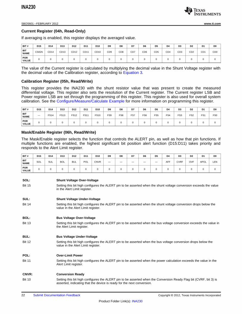
Mask/Enable Register (06h, Read/Write)
The Mask/Enable register selects the function that controls the ALERT pin, as well as how that pin functions. Ifmultiple functions are enabled, the highest significant bit position alert function (D15:D11) takes priority andresponds to the Alert Limit register.
BIT # D15 D14 D13 D12 D11 D10 D9 D8 D7 D6 D5 D4 D3 D2 D1 D0
BITSOL SUL BOL BUL POL CNVR — — — — — AFF CVRF OVF APOL LENNAME
POR0 0 0 0 0 0 0 0 0 0 0 0 0 0 0 0VALUE
SOL: Shunt Voltage Over-Voltage
Bit 15 Setting this bit high configures the ALERT pin to be asserted when the shunt voltage conversion exceeds the valuein the Alert Limit register.
SUL: Shunt Voltage Under-Voltage
Bit 14 Setting this bit high configures the ALERT pin to be asserted when the shunt voltage conversion drops below thevalue in the Alert Limit register.
BOL: Bus Voltage Over-Voltage
Bit 13 Setting this bit high configures the ALERT pin to be asserted when the bus voltage conversion exceeds the value inthe Alert Limit register.
BUL: Bus Voltage Under-Voltage
Bit 12 Setting this bit high configures the ALERT pin to be asserted when the bus voltage conversion drops below thevalue in the Alert Limit register.
POL: Over-Limit Power
Bit 11 Setting this bit high configures the ALERT pin to be asserted when the power calculation exceeds the value in theAlert Limit register.
CNVR: Conversion Ready
Bit 10 Setting this bit high configures the ALERT pin to be asserted when the Conversion Ready Flag bit (CVRF, bit 3) isasserted, indicating that the device is ready for the next conversion.
22 Submit Documentation Feedback Copyright © 2012, Texas Instruments Incorporated
Product Folder Link(s): INA230

INA230
www.ti.com SBOS601 –FEBRUARY 2012
AFF: Alert Function Flag
Bit 4 Although only one alert function at a time can be monitored at the ALERT pin, the Conversion Ready bit (CNVR, bit10) can also be enabled to assert the ALERT pin. Reading the Alert Function Flag bit after an alert can helpdetermine if the alert function was the source of the alert.
When the Alert Latch Enable bit is set to Latch mode, the Alert Function Flag bit clears only when the Mask/Enableregister is read. When the Alert Latch Enable bit is set to Transparent mode, the Alert Function Flag bit is clearedafter the next conversion that does not result in an alert condition.
CVRF: Conversion Ready Flag
Bit 3 Although the INA230 can be read at any time, and the data from the last conversion are available, this bit isprovided to help coordinate single-shot or triggered conversions. This bit is set after all conversions, averaging, andmultiplications are complete. This bit clears under the following conditions in single-shot mode:
1) Writing to the Configuration register (except for power-down or disable selections)
2.) Reading the Mask/Enable register
OVF: Math Overflow Flag
Bit 2 This bit is set to '1' if an arithmetic operation results in an overflow error; it indicates that current and power datamay be invalid.
APOL: Alert Polarity
Bit 1 Configures the latching feature of the ALERT pin and the flag bits.1 = Inverted (active-high open collector)0 = Normal (active-low open collector) (default)
LEN: Alert Latch Enable
Bit 0 Configures the latching feature of the ALERT pin and flag bits.1 = Latch enabled0 = Transparent (default)
When the Alert Latch Enable bit is set to Transparent mode, the ALERT pin and flag bits reset to their idle stateswhen the fault has been cleared. When the Alert Latch Enable bit is set to Latch mode, the ALERT pin and flag bitsremain active following a fault until the Mask/Enable register has been read.
Alert Limit Register (07h, Read/Write)
The Alert Limit register contains the value used to compare to the register selected in the Mask/Enable registerto determine if a limit has been exceeded.
BIT # D15 D14 D13 D12 D11 D10 D9 D8 D7 D6 D5 D4 D3 D2 D1 D0
BITAUL15 AUL14 AUL13 AUL12 AUL11 AUL10 AUL9 AUL8 AUL7 AUL6 AUL5 AUL4 AUL3 AUL2 AUL1 AUL0NAME
POR0 0 0 0 0 0 0 0 0 0 0 0 0 0 0 0VALUE
BUS OVERVIEW
The INA230 offers compatibility with both I2C and SMBus interfaces. The I2C and SMBus protocols areessentially compatible with one another.
The I2C interface is used throughout this data sheet as the primary example, with SMBus protocol specified onlywhen a difference between the two systems is discussed. Two bidirectional lines, SCL and SDA, connect theINA230 to the bus. Both SCL and SDA are open-drain connections.
The device that initiates a data transfer is called a master, and the devices controlled by the master are slaves.The bus must be controlled by a master device that generates the serial clock (SCL), controls the bus access,and generates start and stop conditions.
To address a specific device, the master initiates a start condition by pulling the data signal line (SDA) from ahigh to a low logic level while SCL is high. All slaves on the bus shift in the slave address byte on the rising edgeof SCL, with the last bit indicating whether a read or write operation is intended. During the ninth clock pulse, theslave being addressed responds to the master by generating an Acknowledge bit (ACK) and pulling SDA low.
Copyright © 2012, Texas Instruments Incorporated Submit Documentation Feedback 23
Product Folder Link(s): INA230

INA230
SBOS601 –FEBRUARY 2012 www.ti.com
Data transfer is then initiated and eight bits of data are sent, followed by an ACK. During data transfer, SDA mustremain stable while SCL is high. Any change in SDA while SCL is high is interpreted as a start or stop condition.
Once all data have been transferred, the master generates a stop condition, indicated by pulling SDA from low tohigh while SCL is high. The INA230 includes a 28-ms timeout on its interface to prevent locking up the bus.
Serial Bus Address
To communicate with the INA230, the master must first address slave devices using a corresponding slaveaddress byte. The slave address byte consists of seven address bits and a direction bit that indicates whetherthe action is to be a read or write operation.
The INA230 has two address pins: A0 and A1. Table 7 describes the pin logic levels for each of the 16 possibleaddresses. The state of pins A0 and A1 is sampled on every bus communication and should be set before anyactivity on the interface occurs.
Table 7. INA230 Address Pins andSlave Addresses
A1 A0 SLAVE ADDRESS
GND GND 1000000
GND VS 1000001
GND SDA 1000010
GND SCL 1000011
VS GND 1000100
VS VS 1000101
VS SDA 1000110
VS SCL 1000111
SDA GND 1001000
SDA VS 1001001
SDA SDA 1001010
SDA SCL 1001011
SCL GND 1001100
SCL VS 1001101
SCL SDA 1001110
SCL SCL 1001111
Serial Interface
The INA230 operates only as a slave device on both the I2C bus and the SMBus. Connections to the bus aremade through the open-drain I/O lines, SDA and SCL. The SDA and SCL pins feature integratedspike-suppression filters and Schmitt triggers to minimize the effects of input spikes and bus noise. Althoughthere is spike suppression integrated into the digital I/O lines, proper layout should be used to minimize theamount of coupling into the communication lines. This noise introduction could occur from capacitively couplingsignal edges between the two communication lines themselves or from other switching noise sources present inthe system. Routing traces in parallel with ground in between layers on a printed circuit board (PCB) typicallyreduces the effects of coupling between the communication lines. Shielding communication lines in general isrecommended to reduce to possibility of unintended noise coupling into the digital I/O lines that could beincorrectly interpreted as start or stop commands.
The INA230 supports the transmission protocol for Fast (1 kHz to 400 kHz) and High-speed (1 kHz to 3.4 MHz)modes. All data bytes are transmitted most significant byte first.
24 Submit Documentation Feedback Copyright © 2012, Texas Instruments Incorporated
Product Folder Link(s): INA230

Frame 1 Two-Wire Slave Address Byte(1)
Frame 2 Register Pointer Byte
Start By
Master
ACK By
INA230
ACK By
INA230
1 9 1
ACK By
INA230
1
D15 D14 D13 D12 D11 D10 D9 D8
99
SDA
SCL
1 0 0 A3 A2 A1 A0 R/W P7 P6 P5 P4 P3 P2 P1 P0
Frame 4 Data LSByteFrame 3 Data MSByte
ACK By
INA230
Stop By
Master
1
D7 D6 D5 D4 D3 D2 D1 D0
9
Frame 1 Two-Wire Slave Address Byte(1)
Frame 2 Data MSByte(2)
1
Start By
Master
ACK By
INA230
ACK By
Master
From
INA230
1 9 1 9
SDA
SCL
0 0 A3 R/W D15 D14 D13 D12 D11 D10 D9 D8A2 A1 A0
Frame 3 Data LSByte(2)
StopNo ACK By(3)
Master
From
INA230
1 9
D7 D6 D5 D4 D3 D2 D1 D0
INA230
www.ti.com SBOS601 –FEBRUARY 2012
WRITING TO/READING FROM THE INA230
Accessing a specific register on the INA230 is accomplished by writing the appropriate value to the registerpointer. Refer to Table 2 for a complete list of registers and corresponding addresses. The value for the registerpointer (shown in Figure 27) is the first byte transferred after the slave address byte with the R/W bit low. Everywrite operation to the INA230 requires a value for the register pointer.
Writing to a register begins with the first byte transmitted by the master. This byte is the slave address, with theR/W bit low. The INA230 then acknowledges receipt of a valid address. The next byte transmitted by the masteris the address of the register that data will be written to. This register address value updates the register pointerto the desired register. The next two bytes are written to the register addressed by the register pointer. TheINA230 acknowledges receipt of each data byte. The master may terminate data transfer by generating a start orstop condition.
When reading from the INA230, the last value stored in the register pointer by a write operation determineswhich register is read during a read operation. To change the register pointer for a read operation, a new valuemust be written to the register pointer. This write is accomplished by issuing a slave address byte with the R/Wbit low, followed by the register pointer byte. No additional data are required. The master then generates a startcondition and sends the slave address byte with the R/W bit high to initiate the read command. The next byte istransmitted by the slave and is the most significant byte of the register indicated by the register pointer. This byteis followed by an ACK from the master; then the slave transmits the least significant byte. The masteracknowledges receipt of the data byte. The master may terminate data transfer by generating aNot-Acknowledge bit (No ACK) after receiving any data byte, or generating a start or stop condition. If repeatedreads from the same register are desired, it is not necessary to continually send the register pointer bytes; theINA230 retains the register pointer value until it is changed by the next write operation.
Figure 24 and Figure 25 show the write and read operation timing diagrams, respectively. Note that registerbytes are sent most-significant byte first, followed by the least significant byte.
(1) The value of the slave address byte is determined by the settings of the A0 and A1 pins. Refer to Table 7.
Figure 24. Timing Diagram for Write Word Format
(1) The value of the slave address byte is determined by the settings of the A0 and A1 pins. Refer to Table 7.
(2) Read data are from the last register pointer location. If a new register is desired, the register pointer must be updated.See Figure 27.
(3) ACK by Master can also be sent.
Figure 25. Timing Diagram for Read Word Format
Copyright © 2012, Texas Instruments Incorporated Submit Documentation Feedback 25
Product Folder Link(s): INA230

Frame 1 SMBus ALERT Response Address Byte Frame 2 Slave Address Byte(1)
Start By
Master
ACK By
INA230
From
INA230
NACK By
Master
Stop By
Master
1 9 1 9
SDA
SCL
ALERT
0 0 0 1 1 0 0 R/W 1 0 0 A3 A2 A1 A0 0
Frame 1 Two-Wire Slave Address Byte(1)
Frame 2 Register Pointer Byte
1
Start By
Master
ACK By
INA230
ACK By
INA230
1 9 1 9
SDA
SCL
0 0 A3 A2 A1 A0 R/W P7 P6 P5 P4 P3 P2 P1 P0 Stop
¼
INA230
SBOS601 –FEBRUARY 2012 www.ti.com
Figure 26 shows the timing diagram for the SMBus alert response operation. Figure 27 illustrates a typicalregister pointer configuration.
(1) The value of the slave address byte is determined by the settings of the A0 and A1 pins. Refer to Table 7.
Figure 26. Timing Diagram for SMBus Alert
(1) The value of the slave address byte is determined by the settings of the A0 and A1 pins. Refer to Table 7.
Figure 27. Typical Register Pointer Set
26 Submit Documentation Feedback Copyright © 2012, Texas Instruments Incorporated
Product Folder Link(s): INA230

SCL
SDA
t(LOW)tR tF t(HDSTA)
t(HDSTA)
t(HDDAT) t(SUDAT)
t(HIGH) t(SUSTA)t(SUSTO)
t(BUF)
S SP P
INA230
www.ti.com SBOS601 –FEBRUARY 2012
High-Speed I2C Mode
When the bus is idle, both the SDA and SCL lines are pulled high by the pull-up devices. The master generatesa start condition followed by a valid serial byte containing High-Speed (HS) master code 00001XXX. Thistransmission is made in fast (400 kHz) or standard (100 kHz) (F/S) mode at no more than 400 kHz. The INA230does not acknowledge the HS master code, but does recognize it and switches its internal filters to support3.4-MHz operation.
The master then generates a repeated start condition (a repeated start condition has the same timing as the startcondition). After this repeated start condition, the protocol is the same as F/S mode, except that transmissionspeeds up to 3.4 MHz are allowed. Instead of using a stop condition, repeated start conditions should be used tosecure the bus in HS-mode. A stop condition ends the HS-mode and switches all the internal filters of theINA230 to support the F/S mode.
Figure 28. Bus Timing Diagram
Bus Timing Diagram DefinitionsFAST MODE HIGH-SPEED MODE
PARAMETER MIN MAX MIN MAX UNITS
SCL operating frequency f(SCL) 0.001 0.4 0.001 3.4 MHz
Bus free time between stop and start t(BUF) 600 160 nsconditions
Hold time after repeated START condition. t(HDSTA) 100 100 nsAfter this period, the first clock is generated.
Repeated start condition setup time t(SUSTA) 100 100 ns
STOP condition setup time t(SUSTO) 100 100 ns
Data hold time t(HDDAT) 0 0 ns
Data setup time t(SUDAT) 100 10 ns
SCL clock low period t(LOW) 1300 160 ns
SCL clock high period t(HIGH) 600 60 ns
Clock/data fall time tF 300 160 ns
Clock/data rise time tR 300 160 ns
Clock/data rise time for SCLK ≤ 100 kHz tR 1000 ns
Copyright © 2012, Texas Instruments Incorporated Submit Documentation Feedback 27
Product Folder Link(s): INA230

INA230
SBOS601 –FEBRUARY 2012 www.ti.com
SMBus Alert Response
The INA230 is designed to respond to the SMBus alert response address. The SMBus alert response provides aquick fault identification for simple slave devices. When an alert occurs, the master can broadcast the alertresponse slave address (0001 100) with the Read/Write bit set high. Following this alert response, any slavedevices that generated an alert identify themselves by acknowledging the alert response and sending theirrespective address on the bus.
The alert response can activate several different slave devices simultaneously, similar to the I2C general call. Ifmore than one slave attempts to respond, bus arbitration rules apply. The losing device does not generate anacknowledge and continues to hold the ALERT line low until the interrupt is cleared.
28 Submit Documentation Feedback Copyright © 2012, Texas Instruments Incorporated
Product Folder Link(s): INA230

PACKAGE OPTION ADDENDUM
www.ti.com 11-Aug-2017
Addendum-Page 1
PACKAGING INFORMATION
Orderable Device Status(1)
Package Type PackageDrawing
Pins PackageQty
Eco Plan(2)
Lead/Ball Finish(6)
MSL Peak Temp(3)
Op Temp (°C) Device Marking(4/5)
Samples
INA230AIRGTR ACTIVE VQFN RGT 16 3000 Green (RoHS& no Sb/Br)
CU NIPDAU Level-2-260C-1 YEAR -40 to 125 I230
INA230AIRGTT ACTIVE VQFN RGT 16 250 Green (RoHS& no Sb/Br)
CU NIPDAU Level-2-260C-1 YEAR -40 to 125 I230
(1) The marketing status values are defined as follows:ACTIVE: Product device recommended for new designs.LIFEBUY: TI has announced that the device will be discontinued, and a lifetime-buy period is in effect.NRND: Not recommended for new designs. Device is in production to support existing customers, but TI does not recommend using this part in a new design.PREVIEW: Device has been announced but is not in production. Samples may or may not be available.OBSOLETE: TI has discontinued the production of the device.
(2) RoHS: TI defines "RoHS" to mean semiconductor products that are compliant with the current EU RoHS requirements for all 10 RoHS substances, including the requirement that RoHS substancedo not exceed 0.1% by weight in homogeneous materials. Where designed to be soldered at high temperatures, "RoHS" products are suitable for use in specified lead-free processes. TI mayreference these types of products as "Pb-Free".RoHS Exempt: TI defines "RoHS Exempt" to mean products that contain lead but are compliant with EU RoHS pursuant to a specific EU RoHS exemption.Green: TI defines "Green" to mean the content of Chlorine (Cl) and Bromine (Br) based flame retardants meet JS709B low halogen requirements of <=1000ppm threshold. Antimony trioxide basedflame retardants must also meet the <=1000ppm threshold requirement.
(3) MSL, Peak Temp. - The Moisture Sensitivity Level rating according to the JEDEC industry standard classifications, and peak solder temperature.
(4) There may be additional marking, which relates to the logo, the lot trace code information, or the environmental category on the device.
(5) Multiple Device Markings will be inside parentheses. Only one Device Marking contained in parentheses and separated by a "~" will appear on a device. If a line is indented then it is a continuationof the previous line and the two combined represent the entire Device Marking for that device.
(6) Lead/Ball Finish - Orderable Devices may have multiple material finish options. Finish options are separated by a vertical ruled line. Lead/Ball Finish values may wrap to two lines if the finishvalue exceeds the maximum column width.
Important Information and Disclaimer:The information provided on this page represents TI's knowledge and belief as of the date that it is provided. TI bases its knowledge and belief on informationprovided by third parties, and makes no representation or warranty as to the accuracy of such information. Efforts are underway to better integrate information from third parties. TI has taken andcontinues to take reasonable steps to provide representative and accurate information but may not have conducted destructive testing or chemical analysis on incoming materials and chemicals.TI and TI suppliers consider certain information to be proprietary, and thus CAS numbers and other limited information may not be available for release.
In no event shall TI's liability arising out of such information exceed the total purchase price of the TI part(s) at issue in this document sold by TI to Customer on an annual basis.

PACKAGE OPTION ADDENDUM
www.ti.com 11-Aug-2017
Addendum-Page 2

TAPE AND REEL INFORMATION
*All dimensions are nominal
Device PackageType
PackageDrawing
Pins SPQ ReelDiameter
(mm)
ReelWidth
W1 (mm)
A0(mm)
B0(mm)
K0(mm)
P1(mm)
W(mm)
Pin1Quadrant
INA230AIRGTR VQFN RGT 16 3000 330.0 12.4 3.3 3.3 1.1 8.0 12.0 Q2
INA230AIRGTT VQFN RGT 16 250 180.0 12.4 3.3 3.3 1.1 8.0 12.0 Q2
PACKAGE MATERIALS INFORMATION
www.ti.com 11-Aug-2017
Pack Materials-Page 1

*All dimensions are nominal
Device Package Type Package Drawing Pins SPQ Length (mm) Width (mm) Height (mm)
INA230AIRGTR VQFN RGT 16 3000 367.0 367.0 35.0
INA230AIRGTT VQFN RGT 16 250 210.0 185.0 35.0
PACKAGE MATERIALS INFORMATION
www.ti.com 11-Aug-2017
Pack Materials-Page 2


www.ti.com
PACKAGE OUTLINE
C
16X 0.300.18
1.68 0.07
16X 0.50.3
1 MAX
(0.2) TYP
0.050.00
12X 0.5
4X1.5
A 3.12.9
B
3.12.9
VQFN - 1 mm max heightRGT0016CPLASTIC QUAD FLATPACK - NO LEAD
4222419/B 11/2016
PIN 1 INDEX AREA
0.08
SEATING PLANE
1
49
12
5 8
16 13
(OPTIONAL)PIN 1 ID 0.1 C A B
0.05
EXPOSEDTHERMAL PAD
SYMM
SYMM
NOTES: 1. All linear dimensions are in millimeters. Any dimensions in parenthesis are for reference only. Dimensioning and tolerancing per ASME Y14.5M. 2. This drawing is subject to change without notice. 3. The package thermal pad must be soldered to the printed circuit board for thermal and mechanical performance.
SCALE 3.600

www.ti.com
EXAMPLE BOARD LAYOUT
0.07 MINALL AROUND
0.07 MAXALL AROUND
16X (0.24)
16X (0.6)
( 0.2) TYPVIA
12X (0.5)
(2.8)
(2.8)
(0.58)TYP
( 1.68)
(R0.05)ALL PAD CORNERS
(0.58) TYP
VQFN - 1 mm max heightRGT0016CPLASTIC QUAD FLATPACK - NO LEAD
4222419/B 11/2016
SYMM
1
4
5 8
9
12
1316
SYMM
LAND PATTERN EXAMPLESCALE:20X
NOTES: (continued) 4. This package is designed to be soldered to a thermal pad on the board. For more information, see Texas Instruments literature number SLUA271 (www.ti.com/lit/slua271).5. Vias are optional depending on application, refer to device data sheet. If any vias are implemented, refer to their locations shown on this view. It is recommended that vias under paste be filled, plugged or tented.
SOLDER MASKOPENING
METAL UNDERSOLDER MASK
SOLDER MASKDEFINED
METAL
SOLDER MASKOPENING
SOLDER MASK DETAILS
NON SOLDER MASKDEFINED
(PREFERRED)

www.ti.com
EXAMPLE STENCIL DESIGN
16X (0.6)
16X (0.24)
12X (0.5)
(2.8)
(2.8)
( 1.55)
(R0.05) TYP
VQFN - 1 mm max heightRGT0016CPLASTIC QUAD FLATPACK - NO LEAD
4222419/B 11/2016
NOTES: (continued) 6. Laser cutting apertures with trapezoidal walls and rounded corners may offer better paste release. IPC-7525 may have alternate design recommendations.
SYMM
ALL AROUNDMETAL
SOLDER PASTE EXAMPLEBASED ON 0.125 mm THICK STENCIL
EXPOSED PAD 17:
85% PRINTED SOLDER COVERAGE BY AREA UNDER PACKAGESCALE:25X
SYMM
1
4
5 8
9
12
1316
17

IMPORTANT NOTICE
Texas Instruments Incorporated (TI) reserves the right to make corrections, enhancements, improvements and other changes to itssemiconductor products and services per JESD46, latest issue, and to discontinue any product or service per JESD48, latest issue. Buyersshould obtain the latest relevant information before placing orders and should verify that such information is current and complete.TI’s published terms of sale for semiconductor products (http://www.ti.com/sc/docs/stdterms.htm) apply to the sale of packaged integratedcircuit products that TI has qualified and released to market. Additional terms may apply to the use or sale of other types of TI products andservices.Reproduction of significant portions of TI information in TI data sheets is permissible only if reproduction is without alteration and isaccompanied by all associated warranties, conditions, limitations, and notices. TI is not responsible or liable for such reproduceddocumentation. Information of third parties may be subject to additional restrictions. Resale of TI products or services with statementsdifferent from or beyond the parameters stated by TI for that product or service voids all express and any implied warranties for theassociated TI product or service and is an unfair and deceptive business practice. TI is not responsible or liable for any such statements.Buyers and others who are developing systems that incorporate TI products (collectively, “Designers”) understand and agree that Designersremain responsible for using their independent analysis, evaluation and judgment in designing their applications and that Designers havefull and exclusive responsibility to assure the safety of Designers' applications and compliance of their applications (and of all TI productsused in or for Designers’ applications) with all applicable regulations, laws and other applicable requirements. Designer represents that, withrespect to their applications, Designer has all the necessary expertise to create and implement safeguards that (1) anticipate dangerousconsequences of failures, (2) monitor failures and their consequences, and (3) lessen the likelihood of failures that might cause harm andtake appropriate actions. Designer agrees that prior to using or distributing any applications that include TI products, Designer willthoroughly test such applications and the functionality of such TI products as used in such applications.TI’s provision of technical, application or other design advice, quality characterization, reliability data or other services or information,including, but not limited to, reference designs and materials relating to evaluation modules, (collectively, “TI Resources”) are intended toassist designers who are developing applications that incorporate TI products; by downloading, accessing or using TI Resources in anyway, Designer (individually or, if Designer is acting on behalf of a company, Designer’s company) agrees to use any particular TI Resourcesolely for this purpose and subject to the terms of this Notice.TI’s provision of TI Resources does not expand or otherwise alter TI’s applicable published warranties or warranty disclaimers for TIproducts, and no additional obligations or liabilities arise from TI providing such TI Resources. TI reserves the right to make corrections,enhancements, improvements and other changes to its TI Resources. TI has not conducted any testing other than that specificallydescribed in the published documentation for a particular TI Resource.Designer is authorized to use, copy and modify any individual TI Resource only in connection with the development of applications thatinclude the TI product(s) identified in such TI Resource. NO OTHER LICENSE, EXPRESS OR IMPLIED, BY ESTOPPEL OR OTHERWISETO ANY OTHER TI INTELLECTUAL PROPERTY RIGHT, AND NO LICENSE TO ANY TECHNOLOGY OR INTELLECTUAL PROPERTYRIGHT OF TI OR ANY THIRD PARTY IS GRANTED HEREIN, including but not limited to any patent right, copyright, mask work right, orother intellectual property right relating to any combination, machine, or process in which TI products or services are used. Informationregarding or referencing third-party products or services does not constitute a license to use such products or services, or a warranty orendorsement thereof. Use of TI Resources may require a license from a third party under the patents or other intellectual property of thethird party, or a license from TI under the patents or other intellectual property of TI.TI RESOURCES ARE PROVIDED “AS IS” AND WITH ALL FAULTS. TI DISCLAIMS ALL OTHER WARRANTIES ORREPRESENTATIONS, EXPRESS OR IMPLIED, REGARDING RESOURCES OR USE THEREOF, INCLUDING BUT NOT LIMITED TOACCURACY OR COMPLETENESS, TITLE, ANY EPIDEMIC FAILURE WARRANTY AND ANY IMPLIED WARRANTIES OFMERCHANTABILITY, FITNESS FOR A PARTICULAR PURPOSE, AND NON-INFRINGEMENT OF ANY THIRD PARTY INTELLECTUALPROPERTY RIGHTS. TI SHALL NOT BE LIABLE FOR AND SHALL NOT DEFEND OR INDEMNIFY DESIGNER AGAINST ANY CLAIM,INCLUDING BUT NOT LIMITED TO ANY INFRINGEMENT CLAIM THAT RELATES TO OR IS BASED ON ANY COMBINATION OFPRODUCTS EVEN IF DESCRIBED IN TI RESOURCES OR OTHERWISE. IN NO EVENT SHALL TI BE LIABLE FOR ANY ACTUAL,DIRECT, SPECIAL, COLLATERAL, INDIRECT, PUNITIVE, INCIDENTAL, CONSEQUENTIAL OR EXEMPLARY DAMAGES INCONNECTION WITH OR ARISING OUT OF TI RESOURCES OR USE THEREOF, AND REGARDLESS OF WHETHER TI HAS BEENADVISED OF THE POSSIBILITY OF SUCH DAMAGES.Unless TI has explicitly designated an individual product as meeting the requirements of a particular industry standard (e.g., ISO/TS 16949and ISO 26262), TI is not responsible for any failure to meet such industry standard requirements.Where TI specifically promotes products as facilitating functional safety or as compliant with industry functional safety standards, suchproducts are intended to help enable customers to design and create their own applications that meet applicable functional safety standardsand requirements. Using products in an application does not by itself establish any safety features in the application. Designers mustensure compliance with safety-related requirements and standards applicable to their applications. Designer may not use any TI products inlife-critical medical equipment unless authorized officers of the parties have executed a special contract specifically governing such use.Life-critical medical equipment is medical equipment where failure of such equipment would cause serious bodily injury or death (e.g., lifesupport, pacemakers, defibrillators, heart pumps, neurostimulators, and implantables). Such equipment includes, without limitation, allmedical devices identified by the U.S. Food and Drug Administration as Class III devices and equivalent classifications outside the U.S.TI may expressly designate certain products as completing a particular qualification (e.g., Q100, Military Grade, or Enhanced Product).Designers agree that it has the necessary expertise to select the product with the appropriate qualification designation for their applicationsand that proper product selection is at Designers’ own risk. Designers are solely responsible for compliance with all legal and regulatoryrequirements in connection with such selection.Designer will fully indemnify TI and its representatives against any damages, costs, losses, and/or liabilities arising out of Designer’s non-compliance with the terms and provisions of this Notice.
Mailing Address: Texas Instruments, Post Office Box 655303, Dallas, Texas 75265Copyright © 2017, Texas Instruments Incorporated