low cost, broadband tunable ferroelectric filters for … · low cost, broadband tunable...
TRANSCRIPT

1
LOW COST, BROADBAND TUNABLE FERROELECTRIC FILTERS FOR JTRS CLUSTER 5 APPLICATIONS
Steven Sarraf* SRI International
Eatontown, NJ 07724
Lisa Rulli U.S. Army CERDEC S&TCD
Fort Monmouth, NJ 07703
ABSTRACT
Tunable ferroelectric ceramic capacitors have shown great promise in reducing the size, weight, and power (SWAP) of traditional varactor-based devices. Ferroelectric devices fabricated from Barium Strontium Titanate (BST) have been demonstrated in the laboratory and are just now becoming available for commercial narrowband applications. This paper presents some of the tradeoffs in designing a small form factor (SFF), easily manufacturable, broadband tunable filter utilizing high volume, low-cost BST devices. Development status for filters that cover the 225 MHz to 2.7 GHz frequency range with superior narrowband performance, low in-band insertion loss, and high out-of-band rejection that is directly applicable to the stringent requirements of Joint Tactical Radio System (JTRS) Cluster 5 Software Defined Radio (SDR) is also presented. These Manufacturing Readiness Level (MRL) 4 filters currently provide a 50% reduction in size over traditional approaches, and future short-term plans promise further reductions in unit production cost (UPC) and SWAP.
1. INTRODUCTION
With the pervasive growth of electronic communication devices in the commercial marketplace, such as Wireless Fidelity (WiFi), cell phones, and Bluetooth, the industry has seen tremendous decreases in the SWAP and bill of material (BOM) costs. At the same time, the manufacturability of the devices has also improved. Reductions in the number of components through advanced packaging and integration techniques have reduced the assembly time and increased reliability through decreased solder joints and electrical connections. Test time and calibration have also been reduced through automation and the integration of more functions into the integrated circuits. These are all positive attributes that are desirable in next-generation military communication systems.
There are, however, several aspects that make the transition of these attributes to complex military
communication systems difficult. First, many of the high-volume consumer products are narrowband devices, while next-generation military radios span very wide frequency ranges. Narrowband devices are inherently easier to design, because they require fewer components and less complex matching circuits than the wide bandwidths that must be covered by military devices. Another advantage in consumer electronic devices is that their high volumes and standardized protocols (WiFi, GSM, CDMA) typically prompt the development of specialized chipsets. These parts contribute to lower BOM costs and reductions in circuit board space, leading to smaller, lower cost products. Military radios, on the other hand, are required to support complex waveforms over a very wide spectrum, thus contributing to more complex designs. The circuitry required for these designs is not only hardware and processing power intensive, it can also lead to thermal dissipation problems when packaged in an SFF. The final difference between commercial and military radios is related to operating environment. Although a cell phone must be able to withstand the rigors of the consumer user, including sitting on a hot dashboard in the summer or in a frigid glove box in the winter, these are no comparison to conditions faced by the warfighter in extreme combat conditions. The military environmental requirements, including temperature, shock, and vibration, place constraints on component and product packaging as well as circuit operating tolerances.
The JTRS Cluster 5 SFF is an example of a modern military communication system that must support several complex waveforms, while at the same time meet the stringent warfighter environmental conditions along with SWAP requirements that rival any commercial communication device. The form factors for the various Cluster 5 configurations include handheld and body-borne radios, unattended ground sensors (UGS), and small sensors. Typical bandwidths of operation cover 225 MHz to 2.7 GHz. In order to bridge the gap between components tailored to the commercial marketplace and the needs of military radios, U.S. Army CERDEC initiated a Manufacturing Technology Objective (MTO #04-01). The goal of the MTO is to identify key technologies that can enable the developers of JTRS

Report Documentation Page Form ApprovedOMB No. 0704-0188
Public reporting burden for the collection of information is estimated to average 1 hour per response, including the time for reviewing instructions, searching existing data sources, gathering andmaintaining the data needed, and completing and reviewing the collection of information. Send comments regarding this burden estimate or any other aspect of this collection of information,including suggestions for reducing this burden, to Washington Headquarters Services, Directorate for Information Operations and Reports, 1215 Jefferson Davis Highway, Suite 1204, ArlingtonVA 22202-4302. Respondents should be aware that notwithstanding any other provision of law, no person shall be subject to a penalty for failing to comply with a collection of information if itdoes not display a currently valid OMB control number.
1. REPORT DATE 00 DEC 2004
2. REPORT TYPE N/A
3. DATES COVERED -
4. TITLE AND SUBTITLE Low Cost, Broadband Tunable Ferroelectric Filters For Jtrs Cluster 5 Applications
5a. CONTRACT NUMBER
5b. GRANT NUMBER
5c. PROGRAM ELEMENT NUMBER
6. AUTHOR(S) 5d. PROJECT NUMBER
5e. TASK NUMBER
5f. WORK UNIT NUMBER
7. PERFORMING ORGANIZATION NAME(S) AND ADDRESS(ES) SRI International Eatontown, NJ 07724; U.S. Army CERDEC S&TCDFort Monmouth, NJ 07703
8. PERFORMING ORGANIZATIONREPORT NUMBER
9. SPONSORING/MONITORING AGENCY NAME(S) AND ADDRESS(ES) 10. SPONSOR/MONITOR’S ACRONYM(S)
11. SPONSOR/MONITOR’S REPORT NUMBER(S)
12. DISTRIBUTION/AVAILABILITY STATEMENT Approved for public release, distribution unlimited
13. SUPPLEMENTARY NOTES See also ADM001736, Proceedings for the Army Science Conference (24th) Held on 29 November - 2December 2005 in Orlando, Florida. , The original document contains color images.
14. ABSTRACT
15. SUBJECT TERMS
16. SECURITY CLASSIFICATION OF: 17. LIMITATION OF ABSTRACT
UU
18. NUMBEROF PAGES
17
19a. NAME OFRESPONSIBLE PERSON
a. REPORT unclassified
b. ABSTRACT unclassified
c. THIS PAGE unclassified
Standard Form 298 (Rev. 8-98) Prescribed by ANSI Std Z39-18

2
Cluster 5 radios to design and manufacture SFF devices that have reduced SWAP and UPC. One provision of the MTO vehicle is that it is not intended to develop new technologies; rather it should be used to improve existing off-the-shelf components or manufacturing processes to meet the military requirements.
One such part of the typical Cluster 5 radio that is severely impacted by SWAP requirements, when implemented with traditional components, is the front-end preselector filter. This element is usually built with silicon or gallium arsenide varactor diodes and in order to cover the full operating frequency range, requires many individual sections. A multi-pole switch on both the input and output is required to select the appropriate section. The varactor filter also requires voltage levels in excess of 75V to bias the varactors. This contributes to additional complexity and cost, which directly impacts manufacturability and long-term reliability. Prior work in this field has shown that actual implementations of such a filter consumes approximately eight square inches of printed circuit board space [1]. Given that the overall size of some of the JTRS Cluster 5 form factors are on the same order of magnitude, the varactor diode approach is clearly too large.
Instead of making the filter with varactor diodes, it is possible to implement the same function with capacitors constructed from ferroelectric material, namely thin-film BST. These nanotechnology-based devices were originally developed under the DARPA Frequency Agile Materials for Electronics (FAME) program and have shown great promise in reducing the component sizes in the commercial cellular phone market. They have several properties that make them ideal for the SDR application. First, because the material has a high capacitance density, high value capacitors can be constructed in a small area. The material also lends itself to a high degree of tunability, which is very desirable for the wideband preselector application. And because it is a thin-film based component, it can be manufactured on large wafers using industry standard techniques. This contributes to a lower cost implementation.
This paper describes some of the trade-offs in designing an SFF, easily manufacturable, broadband tunable filter utilizing high-volume, low-cost BST devices. Tying these concepts to an application, the development status of BST-based, wideband filters undertaken by CERDEC is also presented. The filters discussed cover the 225 MHz to 2.7 GHz frequency range with superior narrowband performance, low in-band insertion loss, and high out-of-band rejection that is directly applicable to the stringent requirements of JTRS Cluster 5.
2. WIDEBAND TUNABLE FILTER IMPLEMENTATION
The preselector filter is a critical component in some
wideband radio architectures such as JTRS Cluster 5. A block diagram of a typical wideband radio RF front-end (RFFE) is shown in Figure 1. In the transmit path, the preselector limits the harmonic and spurious content around the modulated RF signal to a narrow band that is only a small percentage of the overall operating frequency before the signal is passed through the power amplifier. A similar function is provided by the preselector in the receive path. In this case, the filter limits the wideband input from the antenna, thus preventing unwanted signals, including co-located transmitters from overloading the front-end amplifiers. The narrowband characteristic of the filter also limits the incoming noise, which increases the radio sensitivity. As is evident from the block diagram, tunability over the entire RF operating spectrum, while maintaining a narrow passband, is critical to the operation of the filter. In the case of the Cluster 5 application, the filter must tune from at least 225 MHz to 2.7 GHz while maintaining a fractional passband bandwidth, which adds to the complexity of the filter.
Fig. 1: Generic wideband SDR RFFE
In theory, it is possible to implement the preselector
filter with a bank of fixed bandwidth filters operating at various center frequencies, connected with a multi-throw switch at the input and output. Such a device is illustrated in Figure 2. Obviously this is both cost- and size-prohibitive, since it could require hundreds of filter sections. The alternative approach is to start with a fixed-frequency bandpass filter topology and modify it to be tunable through the use of variable inductors or capacitors. Several technologies exist to provide electronically variable capacitors [2] – [4], while variable inductors are not as common [5] and [6]. Such an approach is illustrated in Figure 3. Depending on the topology selected and the tuning range of the resonators, several filter sections may be required, adding to the filter complexity. Multi-throw switches at the input and output of the preselector access each individual section.

3
Fig. 2: Switched preselector filter bank
Fig. 3: Tunable resonator bandpass filter section
As described previously, silicon or gallium arsenide varactor diodes are the most common technology used to implement electronically variable capacitors. These devices have been used extensively in both commercial and military equipment, and their manufacturing process is very repeatable and reliable. Changing the capacitance is achieved by varying the DC reverse bias voltage on a diode junction. The voltage changes the junction width and therefore its capacitance. The tuning curve of a typical varactor diode is illustrated in Figure 4. Very large tuning ranges and high Qs can be obtained from these devices. One relative drawback of varactor diode preselectors is the reliance on large tuning voltages to obtain good intermodulation distortion performance. If the DC control voltage is not high enough, the incident RF voltage can force the diode into a forward conduction region. Tuning speeds of these devices is very fast and not a limitation in most JTRS-like applications.
Fig. 4: Varactor diode capacitance versus voltage
characteristic
BST varactors, on the other hand, do not have the same limitations as PN junction varactor diodes. Instead of relying on changing the width of a diode junction, the BST varactor relies on changing the dielectric constant of the BST material. The tuning curve of a typical BST varactor is illustrated in Figure 5. The tuning voltage is much lower than that required for a varactor diode, and this voltage can be either positive or negative. And the BST Q does not decrease with frequency as quickly as it does with the equivalent diode varactor. Because the BST varactor is a relatively new device, it doesn’t have the same reliability and manufacturability track record as conventional diode varactors. There are currently only a few companies producing BST devices in quantity with relatively small-scale distribution to the commercial and military markets. CERDEC has partnered with two BST suppliers to develop wideband tunable filters for use in JTRS SDR applications, with the goal to realize SWAP reductions while improving the device manufacturability and lowering the associated costs.
Fig. 5: BST varactor capacitance versus voltage
characteristic
3. FILTER DESIGN CONSIDERATIONS
Designing a filter that uses BST devices follows essentially the same process as conventional components. The main difference is the increased tuning range and improved harmonic performance over conventional varactor diodes. Specifications for the filter synthesized in this paper are summarized in Table 1. These requirements were derived from the Soldier Level Integrated Communications Environment (SLICE) radio, which is an early representative model of the JTRS Cluster 5 radio that supports the Soldier Radio Waveform (SRW) and will serve as a baseline platform in which to test the filter. The 225 MHz to 2.7 GHz frequency band has been segmented into two bands. The first covers 225 MHz to 1 GHz or two octaves, while the second band covers 1.3 to 2.7 GHz or one octave.

4
Table 1: Preselector Filter Specifications
One of the design challenges is to maintain a constant bandwidth over the entire frequency range. This is difficult because as the operating frequency increases, the percentage bandwidth decreases. This requires an increasing Q with frequency. Taking this requirement into account and considering the other important specifications, including low insertion loss, ripple, delay, and stopband rejection, the best design approach is determined through computer simulation of various filter topologies. One of the companies funded by CERDEC determined that the optimum approach for their BST device process was to split band 1 into six subsections and band 2 into four subsections. The other company determined that their process was most suited to splitting band 1 into two subsections, while it was possible to cover band 2 with only one section. It is important to recognize that the various approaches are dependent on both the BST varactor characteristics and the core RF design expertise. It might be possible to use either topology with either vendor’s BST device.
Developing a potential topology to fulfill the filter requirements requires the use of models that accurately represent the various filter components, including the BST varactors and inductors. During the design process, there may also be some iteration in the design to satisfy the needs of the RF designer who simulates and analyzes the filter performance and the semiconductor engineer who specifies and fabricates the BST device. For example, analysis of the RF voltages that are incident on the various filter components will place constraints on the specification and design of those components. Simply specifying a capacitance range of the BST varactor provides only part of the picture. The semiconductor engineer must also know the voltage stresses that will be placed on the component, because that will impact the actual device implementation and the overall reliability. The interaction between the filter designer and semiconductor engineer may take several iterations to achieve a fully realizable filter topology.
As important as the filter topology is in driving the BST varactor requirements, it also has a role in the overall SWAP reductions that can be achieved. Reducing the number of sections used to cover the full frequency range of the filter will directly contribute to a decrease in the parts count, cost, and size of the filter. In some instances, a smaller, more compact design may impose unforeseen issues such as heat dissipation or interstage coupling resulting from the close proximity of components. Prudent simulation and design engineering is the key to avoiding these issues. In the case of the filters developed for CERDEC, the first generation BST design that took a total of ten separate sections had an overall size reduction of approximately 50% over the traditional diode varactor approach, with almost the same size BOM. The second-generation filter being developed is projected to result in a

5
reduction in real estate of another 50% and an equivalent reduction in the number of components in the BOM. The relative space savings is illustrated in Figure 6 on a circular 4” pod. Note that the varactor diode baseline filter (6a) covers only band 1.
Fig. 6: Filter size reduction (a) baseline - band 1 only
(b) 1st generation BST (c) 2nd generation BST
Part of the power savings that was realized through the filter development program was due to a decrease in the voltage requirements of the two-varactor technologies. As previously mentioned, in some configurations the varactor diodes require higher bias voltages to keep the RF voltage from forward biasing the device. Although the varactor diodes are reverse-biased and consume very little DC current, the actual bias voltages can be in excess of 75V. The BST varactors on the other hand, can operate at higher RF voltages and lower bias levels without degradation in performance [7]. Thus the overall power supply requirements are reduced. This is reflected in a reduction of power supply complexity and potential increases in reliability. The CERDEC filter power supply requirements decreased from a requirement of 75V for the baseline, to 50V for the first generation BST filter. The projected reduction for the second-generation filter is down to 30V. As was the case for the filter size, topology can also play a role in the power supply requirements as determined by the RF voltage levels within the filter.
One overlooked piece of the puzzle in wideband filter design is the digital controller. This portion of the circuit translates the digital tuning information or frequency command to independent analog voltages that control each of the BST devices. Along with providing the digital to analog translation, the controller can also perform temperature compensation to dynamically tune the analog voltage output for changes in ambient temperature. One way of achieving temperature compensation is to characterize the filter response as a function of temperature, and record the analog control voltage required to maintain the filter performance for a set of temperatures. This information is then either stored in a look-up table, or applied to a curve-fitting algorithm. If the look-up table is utilized, the appropriate set of voltages is mapped to the ambient temperature, which is monitored by a thermocouple. Depending on the number of levels, this can require a rather large storage device to hold all of the various voltage/temperature combinations. The other approach is to fit a curve to the
voltage/temperature profile and program the controller to calculate the control voltages based on the ambient operating temperature. The whole issue of temperature compensation should be simplified in the future as the newer, zero-thermal drift BST varactors are developed1.
4. FILTER MANUFACTURABILITY
Manufacturing a filter, or any RF device in general, is often considered a separate task from the initial design and prototype phases. It is, however, something that deserves attention before the initial design has started. Making a few filters work is easy when compared to anticipating all of the problems that can occur in fabricating hundreds or thousands of filters. Some aspects of manufacturability include yield, both BST device and filter, component assembly and handling, and product test.
Designing for yield covers two major areas: the BST varactor and the complete filter. For the BST varactor, yield takes into account all of those problems associated with semiconductor manufacturing. Making sure the process is repeatable from wafer to wafer, as well as across the whole area of the wafer. For example, in some cases particular attention must be given to device characteristics changing at the edges of a wafer due to process variations and handling. Many of these issues can be addressed before the devices have been singulated from the wafer through probing. Closely related to the wafer yield is the device infant mortality and device reliability as they are stressed in the system. The CERDEC MTO addressed some of these issues with one of their contracted BST vendors. Once the failure mechanism was identified and fixed, a burn-in cycle was developed to screen out weak devices before they were populated onto a circuit board. These extra steps contribute to increased cost, but will prevent a device from failing in the filter, which costs more money in either repair or unit replacement costs.
The second important component of yield covers that of the entire filter. A complete tolerance analysis of the filter from an RF perspective ensures that the filter specification will be met even with the worst-case changes in component values. The components at this level include all of the discrete devices that comprise the filter design. Such an analysis is typically performed using an RF simulator such as Agilent Advanced Design System (ADS) [8]. As is the case during the initial design phase, the validity of this analysis is dependent on the accuracy of the models used to represent the discrete filter components.
1 Private conversation with Dr. M. Cole, Army Research Laboratory.

6
Component assembly and handling can have an impact on filter size. To follow the commercial product model, high-volume production techniques such as machine assembly of the printed circuit boards (PCB) instead of hand assembly will reduce assembly costs. One requirement for moving to this manufacturing model is that the machine cell must be able to physically place the components on the board, as dictated by manufacturing placement rules such as minimum component-to-component spacing. This can impact the overall PCB size required for the design. Using these placement design rules during the filter prototype phase also helps to save design iterations. If the designer waits until working prototypes are available to build a production-ready board, valuable time will be spent debugging a new design that may have different parasitic influences on performance due to the changes in component placement. Another issue related to component placement is using both sides of the PCB instead of only one side. Components on two sides of the PCB will save board space, but it may add to assembly cost in the time it takes to flip the board to place the second side components. Clearly the tradeoffs of assembly time versus overall cost, board size, and production quantity must be done early in the design cycle.
Once the filter has been assembled, the final step in the manufacturing process is product test. Along with ensuring that all the components have been installed correctly, the test process includes filter calibration and performance verification. Component installation verification can range from automated optical inspection (AOI) to a full functional test that proves all components were installed correctly based on filter performance [9] and [10]. Involving the manufacturing process engineers early in the layout can prevent many of the common component installation problems, such as tombstoning or solder shorts [11] and [12]. This can help to reduce the time spent on placement verification, allowing the assembly process to rely more heavily on functional and calibration tests.
Filter calibration is highly dependent on the complexity of the design and the performance variation over temperature. As was previously discussed in the controller section, an independent analog voltage controls each BST varactor. This voltage is a function of the desired capacitance and can vary over device lots and operating temperature. An ideal situation is either no change over temperature, or at least a linear change. But this is not always the case. Usually the filter will be calibrated at room temperature and then recalibrated at several other intermediate points. These points (control voltage versus temperature) will then be stored in a lookup table. As the temperature varies, a curve-fitting algorithm that interpolates between the calibration values
will apply the proper control voltage for the desired response. The ideal situation is to use the same look up table for all filters. This is information that can be gathered from simulation of the design, given good component models, and analysis of test data from actual filter measurements.
There are two important points to keep in mind concerning product testing. The first being that the amount of time spent on testing is proportional to cost. Even though the filter test step is automated, minimizing test time will minimize cost. Second, the test engineer must balance the fine line of hardware design verification and actual performance verification. Hardware design verification is something that should be known prior to going into production, while performance verification ensures that the product has been assembled and calibrated correctly and will meet all the filter specifications. In other words, tolerance analysis is best performed before the design goes into full-scale production.
5. CERDEC FILTER DEVELOPMENT STATUS
The U.S. Army CERDEC has recognized that BST
varactor-based wideband tunable filters are critical to achieving the goals set forth by the JTRS Cluster 5 SFF radio. To that end, a dual track filter development program is underway. Two vendors have been selected and are designing filters to interface with the SLICE Radio system. This platform was selected because it supports the SRW, which is one of the major wideband waveforms supported by JTRS Cluster 5. Another benefit of this hardware platform is that it is currently available for early evaluation of the filter prototypes. Table 1 contains a summary of the filter specifications.
As was previously described, the first vendor was able to cover the entire tuning range with a total of ten filter sections. Six sections covered band 1, and band 2 was realized with four sections. A plot showing the typical input and output impedance and insertion loss for band 2 is shown in Figure 7. Band 1 has similar performance.
The space occupied by the filter from this vendor is illustrated in Figure 6b and represents almost a 50% reduction in size over the original varactor diode filter. There were still some significant non-packaging challenges that had to be solved to achieve such a decrease in size. First among these issues was the long-term reliability of the BST devices. It had been observed during extended temperature testing, that the BST varactors were failing when they were subjected to high field strengths. Such a condition can occur when the
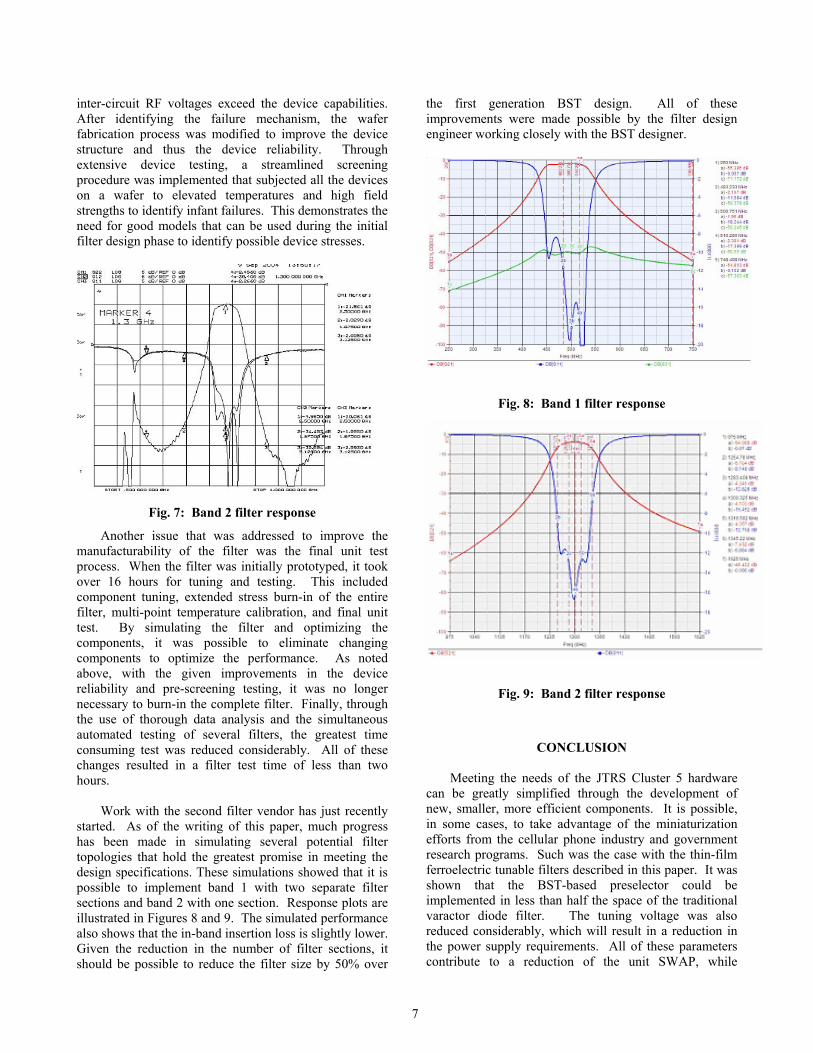
7
inter-circuit RF voltages exceed the device capabilities. After identifying the failure mechanism, the wafer fabrication process was modified to improve the device structure and thus the device reliability. Through extensive device testing, a streamlined screening procedure was implemented that subjected all the devices on a wafer to elevated temperatures and high field strengths to identify infant failures. This demonstrates the need for good models that can be used during the initial filter design phase to identify possible device stresses.
Fig. 7: Band 2 filter response
Another issue that was addressed to improve the manufacturability of the filter was the final unit test process. When the filter was initially prototyped, it took over 16 hours for tuning and testing. This included component tuning, extended stress burn-in of the entire filter, multi-point temperature calibration, and final unit test. By simulating the filter and optimizing the components, it was possible to eliminate changing components to optimize the performance. As noted above, with the given improvements in the device reliability and pre-screening testing, it was no longer necessary to burn-in the complete filter. Finally, through the use of thorough data analysis and the simultaneous automated testing of several filters, the greatest time consuming test was reduced considerably. All of these changes resulted in a filter test time of less than two hours.
Work with the second filter vendor has just recently started. As of the writing of this paper, much progress has been made in simulating several potential filter topologies that hold the greatest promise in meeting the design specifications. These simulations showed that it is possible to implement band 1 with two separate filter sections and band 2 with one section. Response plots are illustrated in Figures 8 and 9. The simulated performance also shows that the in-band insertion loss is slightly lower. Given the reduction in the number of filter sections, it should be possible to reduce the filter size by 50% over
the first generation BST design. All of these improvements were made possible by the filter design engineer working closely with the BST designer.
Fig. 8: Band 1 filter response
Fig. 9: Band 2 filter response
CONCLUSION
Meeting the needs of the JTRS Cluster 5 hardware can be greatly simplified through the development of new, smaller, more efficient components. It is possible, in some cases, to take advantage of the miniaturization efforts from the cellular phone industry and government research programs. Such was the case with the thin-film ferroelectric tunable filters described in this paper. It was shown that the BST-based preselector could be implemented in less than half the space of the traditional varactor diode filter. The tuning voltage was also reduced considerably, which will result in a reduction in the power supply requirements. All of these parameters contribute to a reduction of the unit SWAP, while

8
maintaining the system performance. While leveraging the advances that have taken place in the commercial market helped to achieve these goals, maintaining a close relationship between the circuit designer, semiconductor device fabricator, and manufacturing engineer is crucial to a successful product launch.
ACKNOWLEDGEMENTS
Agile Materials & Technologies, Inc and Paratek, Inc developed the filters discussed in this paper under the CERDEC Affordable SDR Components for JTRS Cluster 5 MTO #04-01 program.
REFERENCES [1] SLICE Radio band 2 varactor diode filter design. [2] De Los Santos, H.J. and R.J. Richards, “MEMS for
RF/Microwave wireless applications: The next wave,” Microwave Journal, March 2001.
[3] Tombak, A., J.P. Maria, F.T. Avguavives, Z. Jin, G.T. Stauf, A.I. Kingon, and A. Mortazawi, “Voltage-Controlled RF Filters Employing Thin-Film Barium-Strontium-Titanate Tunable Capacitors,” IEEE Trans. Microwave Theory Tech., vol. 51, pp. 462-467.
[4] Uher, J. and W.J.R. Hoefer, “Tunable microwave and millimeter-wave bandpass filters,” IEEE Trans. Microwave Theory Tech., vol. 39, pp. 643-653.
[5] Zine-El-Abidine, I., M. Okoniewski, and J.G. McRory, “A new class of tunable RF MEMS inductors,” IEEE Proceedings of the International Conference on MEMS, NANO and Smart Systems, 2003.
[6] Lubecke, V.M., B. Barber, E. Chan, D. Lopez, M.E. Cross, and P. Gammel, “Self-assembling MEMS variable and fixed RF inductors,” IEEE Trans. Microwave Theory Tech., vol. 49, pp. 2093-2098.
[7] Yoon, Y., D. Kim, M.G. Allen, J.S. Kenney, “A reduced intermodulation distortion tunable ferroelectric capacitor-architecture and demonstration,” IEEE Trans. Microwave Theory Tech., vol. 51, pp. 2568-2576.
[8] Agilent Advanced Design System (ADS), Agilent Technologies, http://eesof.tm.agilent.com/products/adsoview.html
[9] Oresjo, S., “What to consider when selecting the optimal test strategy,” Agilent Technologies White Paper.
[10] Miller, D. S., “Yield Enhancement Solutions with AOI,” Surface Mount Technology, May 2004.
[11] Trip, H., “The persistent problem of tombstoning”, Circuits Assembly, June 2003, pp. 20-22.
[12] Peallat, J.M. and V. Butani, “0201s: An inspection nightmare?,” Circuits Assembly, January 2002, pp. 60-64.
1
Technology to the Warfighter Quicker31 October 2004
Low Cost Broadband Tunable Filters for JTRS Cluster 5 Applications
Army Science Conference 2004Paper GO-05
2 December 2004
Gayle [email protected] Monmouth, NJ
Technology to the Warfighter Quicker31 October 2004
• Military-unique design attributes
• Joint Tactical Radio System (JTRS) Cluster 5 Small Form Fit (SFF)
• Benefits of tunable ferroelectric ceramic capacitors
• SFF tunable filter design tradeoffs
• CERDEC wideband filter development status
Low Cost Broadband Tunable Filters for JTRS ApplicationsAgenda

2
Technology to the Warfighter Quicker31 October 2004
Military- Wide frequency range- JTRS ORD waveforms- Low-volume production- Mobile tactical environment- Ruggedization requirements
Commercial- Narrow frequency range- Standardized protocols- High-volume production- Commercial environment
Low Cost Broadband Tunable Filters for JTRS ApplicationsCommunications System Design Attributes
Technology to the Warfighter Quicker31 October 2004
• JTRS Cluster 5 SFF- Software Defined Radio
- 30 – 2700 MHz Frequency Range
- Approximately 9.5 in3
- Configurations:
» Handheld
» Body-borne radios
» Unattended ground sensors
» Small sensors
Low Cost Broadband Tunable Filters for JTRS ApplicationsPlatform Description

3
Technology to the Warfighter Quicker31 October 2004
- Transmit path: limit harmonic and spurious content around the signal to a narrow bandwidth
- Receive path: limit wideband input from the antenna
Generic wideband SDR RFFE
Low Cost Broadband Tunable Filters for JTRS ApplicationsRF Front-End - Preselector
Technology to the Warfighter Quicker31 October 2004
• Switched preselector filter bank
• Tunable resonator bandpass filter
- Bank of switched preselector filters at various center frequencies
- Utilizes complex multi-pole switches
- Cost and size prohibitive- High parts count
- Modify fixed frequency bandpass filter with variable inductors or capacitors
- Utilizes less complex multi-pole switches
- Electronically variable capacitors are widely available
Low Cost Broadband Tunable Filters for JTRS ApplicationsPreselector Filter Implementations

4
Technology to the Warfighter Quicker31 October 2004
• Silicon or gallium arsenide varactor diode implementation
• Largest size and weight driver for RF Front End (RFFE)
• Requires many individual sections to cover full frequency range
- Multi-pole switch selects appropriate section
• High voltage bias for acceptable intermodulation performance
Low Cost Broadband Tunable Filters for JTRS ApplicationsTraditional Front-End Preselector Filters
Technology to the Warfighter Quicker31 October 2004
• Capacitance changed by varying DC reverse bias voltage on diode junction
• Used extensively for commercial and military applications
• Established manufacturing processes
• Very large tuning ranges• High Q - drops significantly with
frequency• Requires high tuning voltages for
good intermodulation distortion performance
Capacitance versus voltage characteristic
Low Cost Broadband Tunable Filters for JTRS ApplicationsCurrent Technology: Silicon or Gallium Arsenide Varactors

5
Technology to the Warfighter Quicker31 October 2004
• Dielectric constant of the BST material determines the capacitance
• Increased tuning range• Improved harmonic performance• Low positive or negative tuning
voltage • Q decreases moderately with
frequency • Reduced SWAP• Lower power supply requirements• Unproven manufacturability
Capacitance versus voltage characteristic
Low Cost Broadband Tunable Filters for JTRS ApplicationsCutting Edge: Barium Strontium Titinate Varactors
Technology to the Warfighter Quicker31 October 2004
- Maintaining constant bandwidth across frequency range- Integration with digital controller
» Digital tuning word to frequency translation» Temperature compensation
- Requires an increasing Q with frequency- Stopband rejection- Low insertion loss- Ripple- Delay
Low Cost Broadband Tunable Filters for JTRS ApplicationsBST Filter Design Considerations

6
Technology to the Warfighter Quicker31 October 2004
- Yield» BST varactor» Complete filter
- Component assembly and handling» Machine assembly of Printed Circuit Boards (PCB)» Trade-offs in overall cost, board size, production
quantity- Product test
» Verify installation » Filter calibration» Performance verification
Low Cost Broadband Tunable Filters for JTRS ApplicationsBST Filter Manufacturability
Technology to the Warfighter Quicker31 October 2004
Preselector Filter Specifications derived from SLICE radio
Low Cost Broadband Tunable Filters for JTRS ApplicationsCERDEC MTO Filter Requirements

7
Technology to the Warfighter Quicker31 October 2004
• Vendor A- Band 1: 6 subsections- Band 2 : 4 subsections- Over 50% size reduction- Similar Bill of Material
(BOM) as traditional approach
- Requires 50 V power
• Vendor B- Band 1: 2 subsections- Band 2: 1 subsection- Over 75% size reduction- Projected to reduce BOM
by 50%- Requires 30 V power
Low Cost Broadband Tunable Filters for JTRS ApplicationsCERDEC MTO Parallel Development of BST Tunable Filters
Technology to the Warfighter Quicker31 October 2004
Baseline(band 1 only)
1st generation BST 2nd generation BST
Low Cost Broadband Tunable Filters for JTRS ApplicationsCERDEC MTO Prototype Filter Footprint Evolution

8
Technology to the Warfighter Quicker31 October 2004
Vendor A Band 2 Filter Response
Low Cost Broadband Tunable Filters for JTRS ApplicationsVendor A Band 2 Filter Response
Technology to the Warfighter Quicker31 October 2004
Vendor B Band 2 Filter Response
Low Cost Broadband Tunable Filters for JTRS ApplicationsVendor B Band 2 Filter Response

9
Technology to the Warfighter Quicker31 October 2004
•CERDEC Filter Development Summary
- Leveraged advances in commercial technology
- Reduced filter footprint by more than 50%
- Reduced tuning voltage
- Reduced SWAP
- Reduced cost
- Maintained filter performance
Low Cost Broadband Tunable Filters for JTRS ApplicationsCERDEC Meeting PM WIN-T Needs
Technology to the Warfighter Quicker31 October 2004
Maintaining a close relationship between the circuit designer, the semiconductor fabricator and the manufacturing engineer is crucial to a successful product launch!
Low Cost Broadband Tunable Filters for JTRS ApplicationsCERDEC Key to Success