lighting innovation centre - the manufacturer of ... · lighting innovation centre more than 120...
TRANSCRIPT

RESEARCH AND DEVELOPMENT
lighting innovation centre

lighting innovation centre
more than 120 technical and academic lighting experts
a 3600 square metre facility area
4 floors
11 nationalities
7 departments
4 academic and science partnerships
LightinginnovationCentre

lighting QUalitY ShoWrooM
SUpplY chain ManageMent
prodUct ManageMent
lighting SolUtionS
photoMetrY laboratorY
electronic SolUtionS
Mechanical enginiering
coMMercial departMent
head of r&d
laboratorY
eSd laboratorY
deSignopticS
optic laboratorY
Mechanical enginiering
QUalitY ManageMent
LightinginnovationCentre
lighting innovation centre

TH
ERM
OGR
AHPY
TH
ERM
AL C
HARA
CTER
IZAT
ION
& S
ERVI
CES
FO
LLO
W T
HE R
IGHG
T LI
GHT
| 11
In
frar
ed t
herm
ogra
phy
is a
proa
ctiv
e tr
oubl
esho
otin
g an
d pr
edic
tive
mai
nten
ance
to
ol.
In
an
infr
ared
ca
mer
a ca
n be
use
d to
mak
e th
e w
orld
tha
t is
invi
sible
to
the
hum
an
eye
com
e to
life
. Th
erm
ogra
phic
ca
mer
as
dete
ct
radi
atio
n in
the
infr
ared
ran
ge o
f th
e el
ectr
omag
netic
spe
ctru
m (r
ough
ly 9
–14
µm
) an
d pr
oduc
e im
ages
of
that
ra
diat
ion,
ca
lled
ther
mog
ram
s. In
frar
ed r
adia
tion
is em
itted
by
all
obje
cts a
bove
abs
olut
e ze
ro a
ccor
ding
to
th
e St
efan
–Bol
tzm
ann
law
. Th
e am
ount
of
radi
atio
n em
itted
by
an
obje
ct
incr
ease
s w
ith
tem
pera
ture
; th
eref
ore,
the
rmog
raph
y al
low
s us
to
see
varia
tions
in te
mpe
ratu
re. T
o co
rrec
tly d
eter
min
e te
mpe
ratu
re
by
infr
ared
th
erm
ogra
phy
is es
sent
ial
to k
now
em
issiv
ity o
f ea
ch su
rfac
e to
be
stud
ied.
Whe
n vi
ewed
th
roug
h a
ther
mal
im
agin
g ca
mer
a, w
arm
obj
ects
st
and
out
wel
l ag
ains
t co
oler
ba
ckgr
ound
s. As
a
resu
lt,
ther
mog
raph
y is
part
icul
arly
us
eful
to
m
ilita
ry,
elec
tric
al
engi
neer
ing,
m
edic
ine,
ve
terin
ary,
bu
ildin
g in
dust
ry,
secu
rity
guar
d et
c.
PB1 PB2
COMPANY PRESENTATION
We realise that our suppliers are a part
of our success. Their brands represent a
tradition and many of them are synonym
of technological leader in its area. To be
able to come to the top we need to be
supported by the best.
Panasonic
Sharp
Samsung
Cree
Sharp
Citizen
OMS – SupplierS and partnerS
Spend & Supply Strategy
logiSticS
ServiceS
indirect materialS
direct materialS
Sup
po
rtin
g develop
me
nt
pr
op
oSing effec tive Solu
tio
nS
supply chain management
Strategic purchaSin
g
ma
nu
facturability
cuSt
omer
Supp
ort
pro
ject
cal
culationS Strategic cooperatio
n
technology eva
lua
tio
n
th
e beSt
p
ro
du
ct
Cooperation between all divisions
Bringing new ideas
Optimization of R&D processes for commercial
attractiveness
Making the R&D and project commercial output
Running internal and project calculations
THERMAL DEPARTMENT
coNcEPT AND DEsigN
LigHTiNg soLUTioNs
NANoTEcHNoLogy
oPTic DEPARTMENT
ELEcTRoNic DEPARTMENT
MEcHANicAL DEPARTMENT
Active cooling with fan Passive cooling with hea tsink
lighting innovation centre

oPtic DePartMent

oPtic DePartMent
Unique optic designs based
on reflector and lens technologies
optical laboratory

optical partsoptics is the branch of physics which involves the behavior and properties of light, including its interactions with matter and the construction of instruments that use or detect it. luminous active parts of luminaires are optical parts (reflectors, lenses), which changes the light from light source by law of refraction and reflection or a dif-fusers, which changes light distri-bution mostly by diffusion. optical parts are produced from materi-als, which have mirror reflection or direct transmission. for diffuser production are used materials with light diffusion. optical parts based on reflection, changes light by crea-tion image of a light source, which luminance is in due proportion to luminance of used light source (in reality is reflection and transmission less than 1).
on other side diffusers scatter the light by whole surface, where the luminance is equal in all direction (if it is „lambertian“ diffuser) and essentially less than luminance of used light source. luminous active parts differentiate according to op-tical properties of materials, which are used (luminaire production) to reflectors, refractors, diffusers.
luminaire is a device that changes light distribution of a light source, diffuses the light or eventually changes its spectral composition.
this goal is reached by luminous ac-tive parts of luminaire (reflector, dif-fuser, lens, etc.) and auxiliary parts (socket, leads, starter, ballast, etc.) that are designed and constructed for specific light sources.
oMS is strongly focused on the best luminaire performance which is given by optimized and efficient optical parts. We understand that optimized parts are demanded by customer and for this reason we focus to build up department which is able to find solutions on customer demands. optical design is powered by lighttools®. it is a unique optical engineering and de-sign software product that features virtual prototyping, simulation, optimization, and photorealistic renderings of precision illumina-tion applications. the software has adapted solid modeling technol-ogy to accommodate the inherent accuracy required to simulate ray paths of
light as they traverse through and within optical elements and me-chanical structures. the software is straightforward
DePartMent of oPtical DeSign anD PhotoMetric laboratorY

to use, accurate, has the most ad-vanced capabilities commercially available, and supports the tasks of design and engineering iterations in addition to analysis which is one of the most well know software for optical analysis. it gives us unlimited possibilities in optical design and analysis to achieve best results in our product and solutions for our customers.
design of reflectorreflector changes light distribution from a light source by creation im-age of a light source in direction of optical axe.
vice-versa, in arbitrary different di-rection has image of a light source insignificant small dimensions.
We can offer optical design of re-flector base on customer applica-tion. each specific application can has reflector which is optimized according to exact parameters. thanks to knowledge and experi-ences of our engineers supported by powerful software oMS can of-fer different reflector design (Simple shape, plane facets and 3D facets). freedom in creativity includes lin-ear, rotational and freeform optical parts.
DePartMent of oPtical DeSign anD PhotoMetric laboratorY
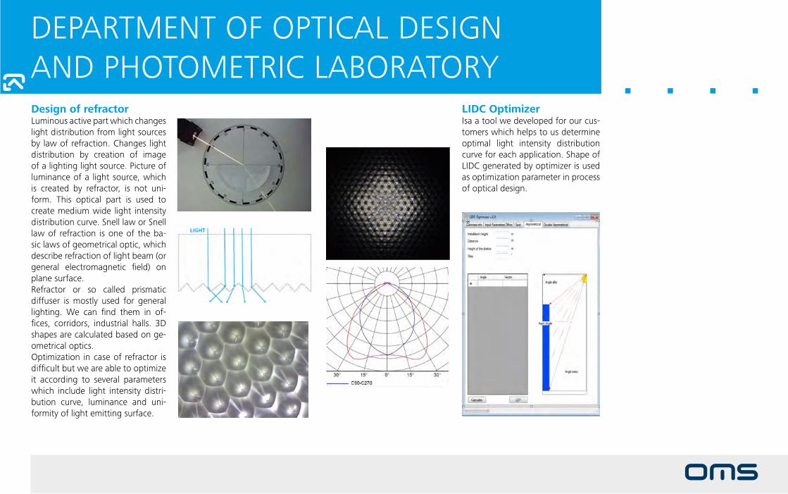
design of refractorluminous active part which changes light distribution from light sources by law of refraction. changes light distribution by creation of image of a lighting light source. Picture of luminance of a light source, which is created by refractor, is not uni-form. this optical part is used to create medium wide light intensity distribution curve. Snell law or Snell law of refraction is one of the ba-sic laws of geometrical optic, which describe refraction of light beam (or general electromagnetic field) on plane surface.refractor or so called prismatic diffuser is mostly used for general lighting. We can find them in of-fices, corridors, industrial halls. 3D shapes are calculated based on ge-ometrical optics. optimization in case of refractor is difficult but we are able to optimize it according to several parameters which include light intensity distri-bution curve, luminance and uni-formity of light emitting surface.
lidc optimizerisa a tool we developed for our cus-tomers which helps to us determine optimal light intensity distribution curve for each application. Shape of liDc generated by optimizer is used as optimization parameter in process of optical design.
DePartMent of oPtical DeSign anD PhotoMetric laboratorY

design of parabolic louversPrimary function of aluminum lou-ver in luminaires is to shield a light source and avoid a glaring. it is used in office luminaires, where is very important high comfort of work environment together with high requirement on lighting instal-lation. aluminum louver is mostly in parabolic shape therefore called „parabolic louver“.
lamellas for linear fluorescent lamps are in parabolic shape, which is optimal for directing of light and avoiding glaring in parallel direc-tion. thanks to well-designed la-mellas is parabolic louver able to full fill requirements of en 12 464-1 light and lighting of interior work-places. Minimal light losses after reflection are because of high re-flective
aluminum surface. high reflective aluminum sheets are equipped by special treatment and material has minimal degradation of reflective surface.
in case of aluminum louver side blades creates a shape of light in-tensity distribution curve in cross section. typical shape of distribu-tion curve is done by side blades. Mostly it has an elliptical shape de-pends on light source position. Side blades shields direct view into light source from a cross section and av-erage luminance has to be below 1500 cd.m-2.
as a company which is very strong in indoor office lighting we know what market and customer needs. to be successful means that is im-portant not only to have a product which is able to full fill all require-ments given by international stand-ards but also performance and cost. We are ready to inspect your parabolic louver and optimize it for the best results. our material library is ready to support your design and to give you best performance for your system.
DePartMent of oPtical DeSign anD PhotoMetric laboratorY

Spectral analysisadvantage of sophisticated soft-ware for optical analysis is possi-bility of a spectral analysis of light sources. input data are real meas-urements by spectrophotometer, which describes a spectrum of a light source and after import repre-sents basic and the most important input for next processing and cal-culations. based on input data we are able to calculate color rendering index (cri), correlation color tem-perature (cct).
after basic calculation we can im-prove quality of light by mixing of light sources with different spec-trum. by determination of spectral ratios we can optimize system ac
cording to cri and cct. We are able to analyze spectral changes by mathematical models without ne-cessity to create prototypes during the development time. thanks to these possibilities we can save time and resources that would otherwise be necessary for the production of prototypes and measurements.
During the process of designing of optical parts is very important to know their parameters. important are parameters, which describe ef-ficiency of optical system, shape of light intensity distribution curve, fWhM (full Width half Maximum), influence of optical part to quality of the light. very important point is also luminance of light emitting sur-face. european standard 12 464-1 light and lighting of interior work-places defines maximum luminance of light emitting surfaces for each application. critical are applications with high requirements for artificial lighting (offices, schools, hospitals, etc.)
DePartMent of oPtical DeSign anD PhotoMetric laboratorY

laboratory servicesour laboratories are one of the best equipped laboratories in the middle and east part of europe. Measure-ments are important for us because to provide relevant measurements is key point of our internal devel-opment. customer demands are not only in case of product but also measurement which they need to convince their customers. in oMS we know how important is exact measurement and this was the rea-son to have all technologies and de-vices in house. flexibility, accuracy, precision and relevant measure-ment service is for us important as the other parts of product develop-ment. We are ready to support your projects by all devices which are necessary for light measurements. goniophotometerrigo 801 is a near-field goniopho-tometer described in international standard en 13 032 – 1 using luxmeter and luminance camera, i.e. photo detector array with imag-ing optical system, which allows to split the luminous surface of the lu
minaire into smaller segments. go-niophotometer is able to measure light intensity Distribution curve (liDc), luminous flux and luminance on light emitting surface.
by this equipment we can create photometric files – eulumdat or ieS, and measurement reports. it is important to be able measure liDc because it is necessary for our Di-alux plugin.
luminance meterthe spot luminance meters are among the best hand meters on the market. the Slr (single lens reflex)
optical system allows precise target-ing and ensures that the viewfinder shows the exact area to be meas-ured, even at very short distances. this makes even precise focussing very easy. in addition to the meas-urement field and the measurement environment, the viewfinder also shows the measured luminance val-ue. the pistol grip makes handling of the unit very secure. Special at-tention has been given to minimize flare and to give precise v(λ) cor-relation (cie relative photopic lumi-nosity curve).
DePartMent of oPtical DeSign anD PhotoMetric laboratorY

luminance analyserthe imaging analysis of light sourc-es and illuminated scenes is get-ting more and more important. the complex evaluation of those scenes requires knowing the lumi-nance distribution within the whole field of view or at least in many se-lected parts of it. Solving the neces-sary measuring tasks by means of measuring devices working point by point either takes an enormous amount of time or is possible only within a coarse raster grid or is not possible at all. thus, the development of spatially resolved radiation receivers, in par-ticular ccD matrix cameras, has en-abled the user to solve measuring problems such as measurements for glare evaluation according to the Ugr method, the analysis of visibility conditions in the road traf-fic at night, emission evaluations of glare sources, the determination of contrasts in illumination situations (workplace) or directly on light sources (e.g. lamps/luminaires, dis-plays, night design, indicators).
luxmeterthe radiolux 111 is a precision hand held instrument for photometric and radiometric meas-urement. it equally serves for laboratory and field applications. Different photometric heads are needed for different kind of illumi-nation which has to be measured according to standard en 12 464-1. We have heads for spherical, semi-cylindrical and horizontal illu-minance measurements.
DePartMent of oPtical DeSign anD PhotoMetric laboratorY
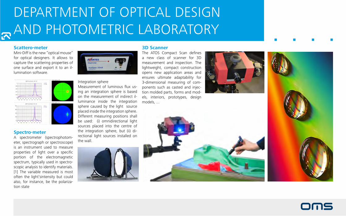
DePartMent of oPtical DeSign anD PhotoMetric laboratorYScattero-meterMini-Diff is the new “optical mouse” for optical designers. it allows to capture the scattering properties of one surface and export it to an il-lumination software.
Spectro-metera spectrometer (spectrophotom-eter, spectrograph or spectroscope) is an instrument used to measure properties of light over a specific portion of the electromagnetic spectrum, typically used in spectro-scopic analysis to identify materials.[1] the variable measured is most often the light’sintensity but could also, for instance, be the polariza-tion state
integration sphereMeasurement of luminous flux us-ing an integration sphere is based on the measurement of indirect il-luminance inside the integration sphere caused by the light source placed inside the integration sphere. Different measuring positions shall be used: (i) omnidirectional light sources placed into the centre of the integration sphere, but (ii) di-rectional light sources installed on the wall.
3d Scannerthe atoS compact Scan defines a new class of scanner for 3D measurement and inspection. the lightweight, compact construction opens new application areas and ensures ultimate adaptability for 3-dimensional measuring of com-ponents such as casted and injec-tion molded parts, forms and mod-els, interiors, prototypes, design models, ...

electronic DePartMent

electronic design of luminaires, system level solutions, measurements
electronic Design
electronic laboratory
optimization & customisation
electronic SolUtionSDePartMent
tunable White control intelligent led module central power Source deebridge
2 IntroductionDEEBRIDGE is a solution comprising an Ethernet to DALI bridge device (Figure 1) and easily operated user interface application. This solution enables intuitive control of luminaires within a DALI installation via an Ethernet network using a PC, tablet or smartphone. The software runs on Windows, Android and iOS.
2.1 Features • An intuitive and user friendly Graphical User Interface (GUI)
• Broadens the possibilities of lighting control
• Enables the real-time control of brightness, colour temperature and RGB output
• The PC application enables date and time functions
2.2 Overview of the deviceThe device comes housed in a standard 2U sized DIN box which allows for installation on electrical switchboards. It is powered by an external 12 V DC Power Source Unit (not standardly supplied with the device but available on request). Figure 2 depicts a simplified connection schematic of the Ethernet to DALI bridge device.
Figure 1: Overview of the Ethernet to DALI bridge device Figure 2: Simplified connection schematic
2.3 Default settingsInitial Ethernet to DALI bridge device TCP/IP and port configuration settings: TCP/IP address: 192.168.1.252 Port: 8421 Default web configuration settings: Username: admin Password: admin
How to change the Ethernet to DALI bridge device IP address and port is covered in 3 Hardware Installation.
DALI -
DALI +
12 V DC
Power status indicatorDALI status indicator
Device status indicator
RESET button
RJ45 Ethernet connector
12 V DCPowerSupplyUnit
+ -
L PE N
LAN 230 V AC
Existing self-powered DALI installation
4
4 Software installation
4.1 Software installation requirementsBefore software installation and setup you will need: • Knowledge about how to perform the IP configuration of your PC, Android or iOS device • Knowledge about the IP configuration used for your LAN • Knowledge about the configuration of your DALI installation
4.2 PC application for Windows NT / XP / 2000 / Vista / 7 / 8
4.2.1 Graphical User Interface overview
Refresh buttonReloads the list of controls
and application settings and reconnects the device
Connection / password settings buttonOpens the IP / port / password
settings window (see 4.2.3 TCP/IP, port and password settings)
Control management buttonOpens the control management tool
(see 5.4 Control management)
Firmware update buttonStarts the device firmware update (see 5.6 Firmware update)
List of individual luminaire controls
List of timer controls
List of scene controls
List of group controls
TunableWhite slider (see 5.3 Control types)
Broadcast dimming slider (see 5.3 Control types)
RGB slider (see 5.3 Control types)
On / off button (see 5.3 Control types)
Status bar Shows information about last connection status
Figure 3: PC application Graphical User Interface7
PB1 PB2

Many well know concepts and tech-nologies have great hidden potential. in the field of electronics, boundaries are being broken not only by new tech-nologies but also by the intelligent use of familiar ideas in new and extraordi-narily innovative ways. nevertheless, we also believe that the success of an idea greatly depends on the time it takes to reach the market. there is no room for a slow and ex-pensive trial and error approach during the transition of an idea into a working product, and neither for semi-finished “engineering” samples when compet-ing with qualified rivals. one way how to run the race faster than the others and win is to run with us. We, members of the oMS electronic Solutions Department, are proud to offer you a comprehensive range of electronic design solutions and services along with our full and continued sup-port. Starting with advanced hardware design and the design of various types of software, to the final combining of them together with a pinch of synergy added in, we are able to provide the system level design of a vast array of customer defined electronic products
and solutions. all stages are checked and verified during various in-house tests, which we can also offer as inde-pendent services.our personal approach and high ex-pertise throughout the whole process of transforming your idea to a profes-sionally formed functional prototype, or any derivative of it, ensures you and your product will be first on the market.furthermore, it will be our pleasure and honour to assist you with our profes-sional review of your own designs at any stage of their development, if you wish.
Solutions hardware design firmware design Software design labware design
Services electronic design review electronic devices rapid prototyping electrical safety tests electronic devices functional tests long-term tests Dali compatibility test
electronic SolUtionS & ServiceS
ELECTRONIC SOLUTIONS & SERVICES
ELECTRONIC SOLUTIONS & SERVICES R&D SERVICES BOOK | 1
Many well know concepts and technologies have great hidden potential. In the field of electronics, boundaries are being broken not only by new technologies but also by the intelligent use of familiar ideas in new and extraordinarily innovative ways.
Nevertheless, we also believe that the success of an idea greatly depends on the time it takes to reach the market. There is no room for a slow and expensive trial and error approach during the transition of an idea into a working product, and neither for semi‐finished “engineering” samples when competing with qualified rivals. One way how to run the race faster than the others and win is to run with us.
We, members of the OMS Electronic Solutions Department, are proud to offer you a comprehensive range of electronic design solutions and services along with our full and continued support. Starting with advanced hardware design and the design of various types of software, to the final combining of them together with a pinch of synergy added in, we are able to provide the system level design of a vast array of customer defined electronic products and solutions. All stages are checked and verified during various in‐house tests, which we can also offer as independent services.
Our personal approach and high expertise throughout the whole process of transforming your idea to a professionally formed functional prototype, or any derivative of it, ensures you and your product will be first on the market.
Furthermore, it will be our pleasure and honour to assist you with our professional review of your own designs at any stage of their development, if you wish.
Solutions
Hardware design Firmware design Software design Labware design
Services
Electronic design review Electronic devices rapid
prototyping Electrical safety tests Electronic devices functional
tests Long‐term tests DALI compatibility test
electronic SolUtionS & ServiceS
harDWare DeSign
firMWare DeSign
SoftWare DeSign
labWare DeSign
electronic DeSign revieW
electronic DeviceS raPiD PrototYPing
electrical SafetY teStS
electronic DeviceS fUnctional teStS
long-terM teStS
Dali coMPatibilitY teStS

harDWare DeSign
Since hardware is the basis of each electronic device creating a func-tional part of its physical body, there is vital need for good hardware design. only well-designed hardware will en-sure the quality, reliability, and long-term stability of your solutions. our spe-cialists in hardware design are keen to develop hardware solutions tailored for your needs utilising the altium Design-er 14 development environment, all in within unbeatable timescale. We have extensive experience in both low-speed digital and analogue designs, and the routing of printed circuit boards (Pcb) with multiple layers. We are mainly ex-perienced in hardware designs tailored for the lighting industry. the hardware design process is a complex combina-tion of tasks, decisions, and repetitions. in general, it is possible to divide the process into seven basic stages:
1. research and analysis of the customer requirements2. Selection of the key components3. Schematic design4. Pcb design5. Prototype6. Documentation and validation7. final product
our engineers are responsible for the complete development process from idea to final product.Well–defined internal processes to-gether with iSo9001 documentation provide us with a fast and almost flaw-less hardware design process.a wide network of cooperating part-ners and suppliers makes component selection easy. they periodically pro-vide us with the latest news from semi-conductor industry and with important notifications, e.g. eol. thanks to this cooperation we have available to us state-of-the-art components along with full support from the suppliers.our fully equipped r&D laboratories al-low us for minimise the time taken to manufacture a prototype.
electronic SolUtionS & ServiceS
harDWare DeSign
firMWare DeSign
SoftWare DeSign
labWare DeSign
electronic DeSign revieW
electronic DeviceS raPiD PrototYPing
electrical SafetY teStS
electronic DeviceS fUnctional teStS
long-terM teStS
Dali coMPatibilitY teStS

firMWare DeSign
Programmable components are used in almost every electronic product found on today’s market. even if only a trivial logic function is requested, the micro-controller unit (McU) is usually chosen to be used instead of discrete com-ponents such as diodes, transistors or operational amplifiers. reasons for this solution are practical:
easier design of Pcb lower bill of material (boM) high reliability flexibility
very important is the economical as-pect: the cost of the McUs is often significantly lower than the cost of the discrete parts necessary for the crea-tion of the logic function requested. firmware development requires close cooperation with the customer, espe-cially when dealing with user interfaces in order to design the device func-tions according to customer wishes. We have been dealing with firmware design for several years and we have expertise mainly in St Microelectronics architecture (both 8 and 32 bit cores). however, if required we are able to work with manufacturers such as Mi-
crochip, atmel, nXP, or any other. We have tight partnership with all the big McU players on the market and their vendors, which gives us direct access to the latest technology available. firm-ware design is closely connected with hardware design. therefore, the firm-ware design usually starts parallel to hardware design, which considerably shortens development time. the time-line that is required for professionally done and thoroughly tested firmware design depends on the complexity of the desired product. for instance, a simple switching function that depends on user input can be done in weeks, while the development of a network with tens of nodes communicating with each other will take months. in order to optimise development time we have at our disposal a library of various ready-to-use solutions such as PWM control, analogue measurements, buck/boost regulation, communication interfaces (Uart, i2c, SPi, etc.), communication protocols (Dc-Plc, USb, Dali, tcP/iP, DMX, etc.) and others. to achieve the creation of efficient and safe firm-ware we are using the standard MiSra c:2012 during the design process.
electronic SolUtionS & ServiceS
harDWare DeSign
firMWare DeSign
SoftWare DeSign
labWare DeSign
electronic DeSign revieW
electronic DeviceS raPiD PrototYPing
electrical SafetY teStS
electronic DeviceS fUnctional teStS
long-terM teStS
Dali coMPatibilitY teStS

SoftWare DeSign
Software represents most important part of the overall system design since the customer can see only the result of the software design art. if hardware is the ‘heart’ of electronic device, soft-ware represents its ‘soul’. We know how to make good software. our ex-periences and references speak for us. We have experiences with software de-sign on different platforms (Windows, linux, Mac oS) to satisfy your require-ments. if you need control software for hardware we can offer you turnkey solution with all parts of the solution (hardware, firmware, software) devel-oped by our developers. We have large experiences with programming also on the mobile platforms (ioS, android), which gives mobility to your solution. as a good reference we can present our control software for a Dali to eth-ernet bridge which is available for Pc as well as for mobile devices.Using smart programming approaches enable us to develop qualitative soft-ware solutions in reasonable time ex-actly according to customer needs. We are using programming techniques such as design patterns to accelerate software design and improve its qual-
ity. Design patterns are proven designs which represent best practices that the programmer must implement in the ap-plication. another good approach is us-ing Unified Modelling language (UMl) which combines techniques from data modelling, business modelling, object modelling, and component modelling. on the other hand, refactoring gives us possibility to maintain software and implement future features faster with less effort.We always do our best and our soft-ware can be characterized by these at-tributes:
Usability
efficiency
Portability
Maintainability
reliability
Security
Understand ability
there are hundreds of programs on the market that can do almost everything you will ever need to do. So why would you need our software? because there are so many programs, serving so many
generalized purposes that it is almost impossible to find one program that does exactly what you want it to do. Moreover, interface segregation prin-ciple tells us, that it is better to have many client-specific interfaces than one general-purpose interface.We provide all-in-one solution for your company from design, development, and deployment to maintenance.
electronic SolUtionS & ServiceS
harDWare DeSign
firMWare DeSign
SoftWare DeSign
labWare DeSign
electronic DeSign revieW
electronic DeviceS raPiD PrototYPing
electrical SafetY teStS
electronic DeviceS fUnctional teStS
long-terM teStS
Dali coMPatibilitY teStS

labWare DeSign
labware is specific kind of software that automates operations in laborato-ries or in industry applications, controls machines and measuring instruments, and acquires data and process it. our solutions are based on the labvieW de-velopment environment, which enables short development cycles, user-friendly gUi design and a large number of li-braries for data acquisition, data pro-cessing, data generation, mathematics, statistics, etc. labvieW (laboratory virtual instru-ment engineering Workbench) is a development environment for a visual programming language from national instruments. it is widely used for in-strument control, data acquisition or industry automation. another advan-tage is that all hardware provided by national instruments is supported by labvieW and using this hardware, the development cycle is even shorter. applicationslabvieW-based applications are very useful in data acquisition, where data acquisition systems can be controlled via Pc or can run as a stand-alone ap-plication. a large number of various
measurement devices from different manufactures can be integrated into the data acquisition system very effec-tively. Data processing is a strongpoint of labvieW. a large set of functions for data processing and mathematical analyses enables fast implementation of the application. after acquisition and processing, data can be easily ex-ported to reports. a very interesting option is connectivity with databases. to control fast processes, fPga-based devices from national instruments can be programmed by labvieW with out-standing performance. for industrial automation, labvieW offers machine control and machine vision. another interesting area is the development of the labvieW device drivers. With all these features, we are offering com-plete turnkey solutions for fully auto-mated customer defined measurement and process units. We can summarise our offer as follows:
Data acquisition systems
automatic measuring systems
instrument control and device driver development
Data processing, mathematical analysis and storage
Machine control and vision
complete turnkey solutions (fully automated customer de fined measurement and pro cess units)
electronic SolUtionS & ServiceS
harDWare DeSign
firMWare DeSign
SoftWare DeSign
labWare DeSign
electronic DeSign revieW
electronic DeviceS raPiD PrototYPing
electrical SafetY teStS
electronic DeviceS fUnctional teStS
long-terM teStS
Dali coMPatibilitY teStS

electronic DeSign revieWELECTRONIC DESIGN REVIEW
ELECTRONIC SOLUTIONS & SERVICES R&D SERVICES BOOK | 6
Electronic design is not always a simple task. The performance of an electrical device is influenced by many factors such as the selection of components, their combination and placement on the PCB, routing on the PCB, interference from the environment, ambient temperature, and many other factors. There are some basic principles that you can learn but the real master of electronic design firstly needs to be experience. Problems connected with electronic design are likely to repeat; therefore, you don’t have to “reinvent the wheel” because we can solve the problem with you and save your time.
Our team consists of highly‐experienced hardware design engineers who are available to help our customers to build high‐performance and highly reliable systems. We can help you to create custom designs based on experience and knowledge. Such support includes provision for reference designs, detailed device and system design rules, design reviews, and general advice.
Integration support is aimed to provide customers with direct access to our engineers who can provide immediate assistance during the integration phase of a product. Typical problems to face might be configuration issues, problems with connections, system performance
issues, general system behaviour issues, or anything else where assistance from experts is needed.
Thanks to our well equipped, ESD protected laboratory we are able to quickly test and diagnose the source of a problem. Our long‐term partnership with the manufacturers of the components allows us to consult your difficulties directly with their application engineers thus rapidly shortening the time needed to find a solution.
Our engineers have a great amount of experience from practical situations and they are open to share it with customers. We also can provide interactive support, hot‐line by email, phone or face‐to‐face consultation.
electronic design is not always a simple task. the performance of an electrical device is influenced by many factors such as the selection of components, their combination and placement on the Pcb, routing on the Pcb, interfer-ence from the environment, ambient temperature, and many other factors. there are some basic principles that you can learn but the real master of electronic design firstly needs to be experience. Problems connected with electronic design are likely to repeat; therefore, you don’t have to “reinvent the wheel” because we can solve the problem with you and save your time. our team consists of highly-experi-enced hardware design engineers who are available to help our customers to build high-performance and highly reli-able systems. We can help you to create custom designs based on experience and knowledge. Such support includes provision for reference designs, de-tailed device and system design rules, design reviews, and general advice. in-tegration support is aimed to provide customers with direct access to our engineers who can provide immediate assistance during the integration phase
of a product. typical problems to face might be configuration issues, problems with connections, system performance issues, general system behaviour issues, or anything else where assistance from experts is needed. thanks to our well equipped, eSD protected laboratory we are able to quickly test and diagnose the source of a problem. our long-term partnership with the manufacturers of the components allows us to consult your difficulties directly with their appli-cation engineers thus rapidly shorten-ing the time needed to find a solution. our engineers have a great amount of experience from practical situations and they are open to share it with cus-tomers. We also can provide interactive support, hot-line by email, phone or face-to-face consultation.
ELECTRONIC DESIGN REVIEW
ELECTRONIC SOLUTIONS & SERVICES R&D SERVICES BOOK | 6
Electronic design is not always a simple task. The performance of an electrical device is influenced by many factors such as the selection of components, their combination and placement on the PCB, routing on the PCB, interference from the environment, ambient temperature, and many other factors. There are some basic principles that you can learn but the real master of electronic design firstly needs to be experience. Problems connected with electronic design are likely to repeat; therefore, you don’t have to “reinvent the wheel” because we can solve the problem with you and save your time.
Our team consists of highly‐experienced hardware design engineers who are available to help our customers to build high‐performance and highly reliable systems. We can help you to create custom designs based on experience and knowledge. Such support includes provision for reference designs, detailed device and system design rules, design reviews, and general advice.
Integration support is aimed to provide customers with direct access to our engineers who can provide immediate assistance during the integration phase of a product. Typical problems to face might be configuration issues, problems with connections, system performance
issues, general system behaviour issues, or anything else where assistance from experts is needed.
Thanks to our well equipped, ESD protected laboratory we are able to quickly test and diagnose the source of a problem. Our long‐term partnership with the manufacturers of the components allows us to consult your difficulties directly with their application engineers thus rapidly shortening the time needed to find a solution.
Our engineers have a great amount of experience from practical situations and they are open to share it with customers. We also can provide interactive support, hot‐line by email, phone or face‐to‐face consultation.
electronic SolUtionS & ServiceS
harDWare DeSign
firMWare DeSign
SoftWare DeSign
labWare DeSign
electronic DeSign revieW
electronic DeviceS raPiD PrototYPing
electrical SafetY teStS
electronic DeviceS fUnctional teStS
long-terM teStS
Dali coMPatibilitY teStS

electronic DeviceS raPiD PrototYPing
ELECTRONIC DEVICES RAPID PROTOTYPING
ELECTRONIC SOLUTIONS & SERVICES R&D SERVICES BOOK | 7
Prototyping is an integral part of the system level design process. Customers can take advantage of our in‐house rapid prototyping services to verify functionality and of their projects. Functional prototypes can identify problems in early design stages, thus minimize risk, reducing development costs, and accelerating development cycles.
We manufacture, assembly and test prototype PCBs and 3D printed or machined mechanical parts such as enclosures according to your inputs in very short time. ESD protected, well equipped laboratory is ready for assembling and testing.
Wrapped together rapid prototyping of various electronic devices provides our customers with competitive advantage.
Following workflow showing rapid prototyping of functional sample of ambient light sensor from previously prepared data. Overall time to create functional prototype is amazing one working day.
PCB DESIGN MICRO MACHINING (2 hrs) ULTRASONIC CLEANING (1 hr)
SOLDER PASTE DISPENSING (0.5 hr) COMPONENTS PLACING (1 hr) INFRARED SOLDERING (0.5 hr)
BARE PCB CLEAN BARE PCB
3D PRINTING (3 hrs) 3D PRINTED & MICROMACHINED PARTS ASSEMBLED PCB
OVERALL TIME = 8 hours = 1 WORKING DAY!!! FUNCTIONAL PROTOTYPE
Prototyping is an integral part of the system level design process. custom-ers can take advantage of our in-house rapid prototyping services to verify functionality and of their projects. functional prototypes can identify problems in early design stages, thus minimize risk, reducing development costs, and accelerating development cycles. We manufacture, assembly and test prototype Pcbs and 3D printed or machined mechanical parts such as enclosures according to your inputs in very short time. eSD protected, well equipped laboratory is ready for assem-bling and testing. Wrapped together rapid prototyping of various electronic devices provides our customers with competitive advantage.following workflow showing rapid prototyping of functional sample of ambient light sensor from previously prepared data. overall time to create functional prototype is amazing one working day.
electronic SolUtionS & ServiceS
harDWare DeSign
firMWare DeSign
SoftWare DeSign
labWare DeSign
electronic DeSign revieW
electronic DeviceS raPiD PrototYPing
electrical SafetY teStS
electronic DeviceS fUnctional teStS
long-terM teStS
Dali coMPatibilitY teStS

ELECTRICAL SAFETY TESTS
ELECTRONIC SOLUTIONS & SERVICES R&D SERVICES BOOK | 8
Electrical safety testing is essential to ensure safe operating standards for any product that uses electricity. Various governments and agencies have developed stringent requirements for electrical products that are sold world‐wide.
In most markets it is mandatory for a product to conform to safety standards promulgated by safety and standard agencies such as UL, CE, VDE, CSA, BSI, and CCC.
To conform to such standards, the product must pass safety tests such as:
High Voltage Test (Dielectric
Voltage‐withstand Test) Insulation Resistance Test Earth Bond Test Leakage Current Test Functionality Test
These tests are described
in IEC 60335, IEC 61010, and many other national and international standards.
In general, IEC 60335 is the most widely applied standard for electrical safety testing, especially for domestic appliances. Many safety testing standards in the world have been based on it.
electrical safety testing is essential to ensure safe operating standards for any product that uses electricity. various governments and agencies have devel-oped stringent requirements for electri-cal products that are sold world-wide. in most markets it is mandatory for a product to conform to safety standards promulgated by safety and standard agencies such as Ul, ce, vDe, cSa, bSi, and ccc. to conform to such stand-ards, the product must pass safety tests such as:
high voltage test (Dielectric voltage-withstand test)
insulation resistance test
earth bond test
leakage current test
functionality test
these tests are described in iec 60335, iec 61010, and many other national and international standards. in general, iec 60335 is the most widely applied standard for electrical safety testing, es-pecially for domestic appliances. Many safety testing standards in the world have been based on it.
electrical SafetY teStS
electronic SolUtionS & ServiceS
harDWare DeSign
firMWare DeSign
SoftWare DeSign
labWare DeSign
electronic DeSign revieW
electronic DeviceS raPiD PrototYPing
electrical SafetY teStS
electronic DeviceS fUnctional teStS
long-terM teStS
Dali coMPatibilitY teStS

electronic DeviceS fUnctional teStSELECTRONIC DEVICES FUNCTIONAL TESTS
ELECTRONIC SOLUTIONS & SERVICES R&D SERVICES BOOK | 9
Each electronic device needs to pass through a testing stage in order to verify its functionality and to characterise its properties. Testing procedures are usually performed several times during the device development as they provide the designer by the feedback which is essential for correct electronic design.
During the functional tests we firstly test the device using the recommended conditions – temperature, input voltage, input signals. All the parameters necessary for proper function of the device are measured. After passing the basic set of measurements, we can test the behaviour of the device when working on the internal edges of recommended conditions.
To reach fast and repeatable measurements we have developed an automatic testing instrument, originally designed for the characterisation of power supplies, but reconfigurable for the measuring of any kind of electronic device. This instrument is composed of a switching power supply, electronic load and four‐channel digital oscilloscope. All these instruments are controlled and automated by a software application made in the LabVIEW development environment.
As an example of the tests the measurement of input voltage range can be mentioned. Input voltage from
the power supply is increasing from zero to maximum input voltage. Electronic load measures output the electrical properties and the software evaluates when the nominal output current is reached. There is also the possibility to gradually decrease input power from maximum to zero. A DC input power option is available too. Another test measures the output voltage range. An electronic load is set as a constant voltage load and stepping voltage from zero. During this process, output power, input power, efficiency and power factor are measured. The advantage of this test is that an input voltage can be set an arbitrary value. Also time dependent device properties can be tested. These properties are turn‐on time, turn‐off time, rise time, fall time, voltage ripple, and current ripple. A useful option is the ability to measure inrush current.
All measured parameters are processed by software and exported to reports. Graphs and tables can be exported to OriginLab or MS Excel, all results are then exported to a Word document and can be saved also as a PDF document. The overview clearly shows the versatility of this automatic measurement system.
ELECTRONIC DEVICES FUNCTIONAL TESTS
ELECTRONIC SOLUTIONS & SERVICES R&D SERVICES BOOK | 9
Each electronic device needs to pass through a testing stage in order to verify its functionality and to characterise its properties. Testing procedures are usually performed several times during the device development as they provide the designer by the feedback which is essential for correct electronic design.
During the functional tests we firstly test the device using the recommended conditions – temperature, input voltage, input signals. All the parameters necessary for proper function of the device are measured. After passing the basic set of measurements, we can test the behaviour of the device when working on the internal edges of recommended conditions.
To reach fast and repeatable measurements we have developed an automatic testing instrument, originally designed for the characterisation of power supplies, but reconfigurable for the measuring of any kind of electronic device. This instrument is composed of a switching power supply, electronic load and four‐channel digital oscilloscope. All these instruments are controlled and automated by a software application made in the LabVIEW development environment.
As an example of the tests the measurement of input voltage range can be mentioned. Input voltage from
the power supply is increasing from zero to maximum input voltage. Electronic load measures output the electrical properties and the software evaluates when the nominal output current is reached. There is also the possibility to gradually decrease input power from maximum to zero. A DC input power option is available too. Another test measures the output voltage range. An electronic load is set as a constant voltage load and stepping voltage from zero. During this process, output power, input power, efficiency and power factor are measured. The advantage of this test is that an input voltage can be set an arbitrary value. Also time dependent device properties can be tested. These properties are turn‐on time, turn‐off time, rise time, fall time, voltage ripple, and current ripple. A useful option is the ability to measure inrush current.
All measured parameters are processed by software and exported to reports. Graphs and tables can be exported to OriginLab or MS Excel, all results are then exported to a Word document and can be saved also as a PDF document. The overview clearly shows the versatility of this automatic measurement system.
each electronic device needs to pass through a testing stage in order to ver-ify its functionality and to characterise its properties. testing procedures are usually performed several times during the device development as they provide the designer by the feedback which is essential for correct electronic design.During the functional tests we firstly test the device using the recommend-ed conditions – temperature, input voltage, input signals. all the param-eters necessary for proper function of the device are measured. after pass-ing the basic set of measurements, we can test the behaviour of the device when working on the internal edges of recommended conditions.to reach fast and repeatable measurements we have developed an automatic testing instrument, originally designed for the characterisation of power supplies, but reconfigurable for the measuring of any kind of electronic device. this instrument is composed of a switch-ing power supply, electronic load and four-channel digital oscilloscope. all these instruments are controlled and automated by a software application made in the labvieW development environment. as an example of the tests the measurement of input voltage
range can be mentioned. input voltage from the power supply is increasing from zero to maximum input voltage. electronic load measures output the electrical properties and the software evaluates when the nominal output current is reached. there is also the possibility to gradually decrease input power from maximum to zero. a Dc input power option is available too. another test measures the output volt-age range. an electronic load is set as a constant voltage load and stepping voltage from zero. During this process, output power, input power, efficiency and power factor are measured. the advantage of this test is that an input voltage can be set an arbitrary value. also time dependent device proper-ties can be tested. these properties are turn-on time, turn-off time, rise time, fall time, voltage ripple, and current ripple. a useful option is the ability to measure inrush current. all measured parameters are processed by software and exported to reports. graphs and tables can be exported to originlab or MS excel, all results are then exported to a Word document and can be saved also as a PDf document. the overview clearly shows the versatility of this au-tomatic measurement system.
electronic SolUtionS & ServiceS
harDWare DeSign
firMWare DeSign
SoftWare DeSign
labWare DeSign
electronic DeSign revieW
electronic DeviceS raPiD PrototYPing
electrical SafetY teStS
electronic DeviceS fUnctional teStS
long-terM teStS
Dali coMPatibilitY teStS

long-terM teStS
Solid State lighting (SSl) technology is growing during this decade and new luminaries based on light emitting Diodes (leD) bring new challenges in testing and characterisation. Modern SSl luminaries offer additional capa-bilities in the control of light properties in comparison with conventional light sources. therefore, the complexity of electronic design is much higher as well as demands on testing.
long-term test system our automatic long-term testing sys-tem was developed to test leD based luminaries. our system was developed to measure in 4 measuring nodes, each with 6 channels (luminaries), which gives us up to 24 luminaries being measured simultaneously. luminaries are powered from a regulated linear power source and measuring devices measure light output, electrical param-eters such as input current, voltage, apparent power, active power, reactive power and power factor. Up to 10 ther-mocouples per channel are available to measure temperature on different parts of the luminaire. this large number of thermocouples fulfils also the high-
est requirements of the largest lumi-naries. the safety aspect is also taken into consideration. each luminaire is powered through a circuit breaker and has a temperature safety relay which turns the fixture off if overheated. this prevents serious damage to the lumi-naire and fully-automated laboratory itself. an interesting option is the set-ting of alarms for each thermocouple separately. these alarms don’t turn off luminaire, but show warnings and log them. this gives higher freedom in luminaire testing. at first, the sys-tem provides a basic functionality test, where the luminaire is running for 72 hours and during this period the tem-perature and light output are logged periodically. the next test is aimed at functionality while the power is turn-ing on and off periodically – frequent switching test. this system enables also endurance tests. this is performed ac-cording to the standard iec 60598-1-12. SSl luminaries often support also some kind of dimming. the most fre-quently used ones can be tested. these are dimming via Dali, 0-10 v, and 1-10 v dimming. Useful is the option to set exponential as well as linear dimming.
a very important parameter, especially in SSl luminaries, is lifetime. this can be basically tested using the same prin-ciples as the functionality test, but over an extended period of time (several thousand hours).
offered tests we can summarise as:
functionality test
frequent switching test
Under-voltage test
over-voltage test
endurance test (iec60598-1-12)
Dimming test (Dali, 0-10v, 1-10v)
lifetime test
all measurements are performed in a room with stabilised temperature of 25 °c, varying not more than ±1 °c.
electronic SolUtionS & ServiceS
harDWare DeSign
firMWare DeSign
SoftWare DeSign
labWare DeSign
electronic DeSign revieW
electronic DeviceS raPiD PrototYPing
electrical SafetY teStS
electronic DeviceS fUnctional teStS
long-terM teStS
Dali coMPatibilitY teStS

Dali coMPatibilitY teStS
Dali stands for Digital addressable lighting interface and is a protocol set out in the technical standard iec 62386. in 2011 the Dali share repre-sented approx. 55% out of all dimma-ble fluorescent control gears in europe (official statistics Zvei - german elec-trics and electrical manufacturers’ as-sociation). this underlines that Dali is clearly becoming the true standard for professional lighting in europe. in ad-dition, international regions recognise and show interest in the Dali technol-ogy. Dali simplicityDali is based on an internationally recognised iec standard for the intelli-gent and easy management of lighting equipment. the standard incorporates several parts that provide control and monitoring functionality for ballasts, emergency gear and leD drivers; ex-panding to lighting controls in the near future. its digital simplicity and flexibility enables customers to create solutions that are easy-to-use, robust, interoperable and above all affordable. Dali has proven its reliability for many years, and will continue to develop and support the growing demands for pro-fessional lighting.
Dali Working group the Dali Wg is a working party of Zvei e.v. set up by leading international manufacturers in the field of digital lamp/luminaire con-trol to promote Dali technology and application. on 23rd november 2013 the general assembly stated new rules for a new Dali working party that will act under the statutes of the german electrical and electronic manufacturer‘s association Zvei based in frankfurt am Main. oMS has been a regular member of Dali since 2012 as a result of our interest in the development of digitally controlled dimmable luminaries and their control devices. Since the estab-lishment of the general assembly in november 2012 we have actively par-ticipated in each Dali group meeting. this gives us an opportunity to influ-ence the Dali standard itself and also certification conditions for new prod-ucts.new rules for Dali logo licensing in 2014 a new logo/licensing process will be agreed to define conditions for proper usage of the Dali logo. each new product has to pass testing by an official Dali tester. already licensed products can be asked for retesting by Dali Wg, either randomly or after a
problem with product has been report-ed. this prevents possible cheating by manufacturer when making changes to their products. the Dali logo will be trademarked; therefore, legal action is possible in the case of unauthorised us-age of the logo. Dali certification procedures in Sep-tember 2013 we purchased a Dali tester. this gives us the opportunity to perform Dali testing in-house. the basic Dali tester configuration can be extended for further testing therefore we can provide even stricter testing than that required by standards. the results of testing (if positive) can be sent directly to Dali Wg for the certi-fication process in order to obtain the Dali logo. oMS intends to become an official Dali testing house to make easier and shorten the time taken for the whole certification process. as an active member of the Dali Wg, oMS has direct access to the newest version of test sequences and standards, thus ensuring the most up-to-date testing conditions.
electronic SolUtionS & ServiceS
harDWare DeSign
firMWare DeSign
SoftWare DeSign
labWare DeSign
electronic DeSign revieW
electronic DeviceS raPiD PrototYPing
electrical SafetY teStS
electronic DeviceS fUnctional teStS
long-terM teStS
Dali coMPatibilitY teStS

therMal DePartMent

Thermal Imager
IR ThermometerDAQ System
EMC Testing Device
Thermal chamber 1: room temperature to 70°C Thermal chamber 2: -70 °C to 180°C
therMal DePartMent
Passive cooling
active cooling
elektroaerodynamik cooling solutions
thermal test center
(new testing facility for air handling luminiares)
thermal Studies and analysis
At 50°C of ambient temperature, the 65mA version could be easily to cool down by fin heat sink (7kg). The case
temperature of LED is 77.5°C by evaluation. However, the 90mA version may not be easy to solve or cost effective
by using conventional passive cooling only. For this situation, the length of fin is extended to 73mm and the total
weight of the fin heat sink is increased to 9.3kg. The maximum case temperature of LEDs at 90mA is 61.3 and 76.3
for ambient 35°C and 50°C (Figure 4.2 and Table 4.1). The results satisfied thermal and optical requirements.
(a)
(b)
Figure 4.1: Geometry of fin heat sink with the length of fin (a) 37 mm and (b) 73 mm
Case 1
Case 2
Case 3
Figure 4.2: Under 35°C of ambient temperature, case temperature of LED
of (a) Case 1 is 65°C; (b) Case 2 is 54.1°C and (c) Case 3 is 61.3°C.
Study
Case 1 Case 2
Case 3 Unit
Forward current
65 65
90 mA
Weight of heat sink
7.0 9.3
9.3 kg
Fin length
37 73
73 mm
TC of LED at 35°C 62.6
54.1 61.3
°C
at 50°C (evaluation) 80.0 69.1
76.3 °C
Total luminous flux at 3000K: V rank*
at 35°C 12,300 129,00
16,800 lm
at 50°C (evaluation) 11,880 12,180
16,320 lm
Table 4.1: Result summary of using fin heat sink
*Based on Samsung LED MP23L Design Tool
With fully shrouded configuration, the air forced to flow through the fin of the heat sink. Without shrouded
configuration, the partial air flow would bypass the heat sink. Figure 4.10 clearly shows this phenomenon with and
without shrouded configurations under natural convection.
(a)
(b)
(c)
(d)
Figure 4.10: Pattern of air flow in natural convection: (a) circular heat sink with no shrouded configuration; circular
heat sink with fully shrouded configuration; (c) platefin heat sink with no shrouded configuration and (d) platefin
heat sink with fully shrouded configuration. In this study, the reversed configuration of the heat shield would be studied. In this section, the clearance is between
the fin tip of the heat sink and the heat shield. Four different fin tiptoshield clearances, cfs, were performed with
various inlet velocity from 0.0 m/s to 3.0 m/s. They are 6 mm, 12.5 mm, 25 mm and 37.5 mm. The geometries are
shown in Figure 5.1.
cfs = 6 mm cfs = 12.5 mm cfs = 25 mm cfs = 37.5 mm
cfs = 6 mm cfs = 12.5 mm cfs = 25 mm cfs = 37.5 mm
Figure 5.1: Geometries of reversed configurations. Note: cfs = fin tiptoshield clearance.
The combinations were performed and the thermal resistances with c and cfs are identical with circular heat sink.
However, the pressure drop was higher which can be up to 30% under forced convection but still lower than fully
shrouded configuration. Due to the further pressure drop, the performance of heat transfer by using fin tiptoshied
would be worse than the shieldtoduct configurations. Figure 5.2 shows the fin tiptoshield and shieldtoduck
comparison on thermal resistance and pressure drop.
Tung Ching Lui
Thermal Design Engineer, Resaerch & Developement, OMS, spol. s r. o.
Dojč 419, 906 02 Dojč, Slovakia
Under the regulation, the printed circuit board for lighting is required to label the TC point and the maximum case
temperature. There are few methods to find out the maximum case temperature of PCB such as thermal
measurement but it may be costly and time consuming. In this paper, numerical study is performed to verify the
maximum case temperature of LED and a study regarding to the various cooling systems which effect on the case
temperature of FR4 PCB.
FR4 based PCB is an example for verifing the thermal resistance between the TC_solder and the TC_PCB (θSP). To
simplify the simulation and reduce the calculation time, Aluminum block is acted as cooling system with various
geometries and it is mounted at the backside of PCB to investigate how much impact on the θSP and TC_PCB. Two
copper layers of FR4 based PCB were modeled and each LED has 16 copper vias for heat removing. The thickness
of copper layer is 76m. The thickness of FR4 is 1.5 mm. The outer diameter of thermal via is 0.3 mm and the
copper plating thickness is 75m. Thermal power of each LED is 0.152W and total number of LEDs is 36.
(a) (b)
(c)
Figure 2.1: Geometry of simulation model.
Three different geometries were presented in Figure 2.2. Case 1 is to investigate the effect with different height of
Aluminum block. Case 2 is to vary the width of the Aluminum block and Case 3 is to keep the temperature of
Aluminum as constant. Each geometry would be tested three configurations. Maximum case temperature of solder
(TC_solder) and case temperature of PCB (TC_PCB) were monitored and thermal resistance of solder and PCB (θSP) and
TC_PCB at TC_solder = 80°C would be evaluated by the simulation results and Equation 1.
THERMAL DESIGN
Department of Mechanical Engineering
Thermal Studies
and Analysis
THERMAL DESIGN
Department of Mechanical Engineering
Thermal Studies
and Analysis
Thermal Studies
and Analysis
Active cooling with fan Passive cooling with hea tsink
Hybrid streetlight with Polypropylene Copolymer (PPCO)
Thermal Imager
IR ThermometerDAQ System
EMC Testing Device
Thermal chamber 1: room temperature to 70°C Thermal chamber 2: -70 °C to 180°C

therMal characteriZation & ServiceS
teMPeratUre cYcling
PoWer cYcling
SteaDY State oPerating life
high/loW teMPeatUre Storage life
therMal SiMUlation
therMo-Mechanical SiMUlation
flUiD floW bUilDing heating & ventilation
force PreDiction
therMograhPY gloW Wire teSting
THERMAL CHARACTERIZATION & SERVICES
THERMAL CHARACTERIZATION & SERVICES FOLLOW THE RIGHGT LIGHT | 1
With the continuing industry trends towards smaller, faster, and higher power devices, thermal management is becoming increasingly important. After all, higher device performance can come at a price - higher temperatures and lower reliability - if thermal considerations aren't carefully weighed. Not only are devices trending smaller but the boards they mount onto are also shrinking. Placing the units closer and closer together on smaller boards helps lower overall system size and cost, and improves electrical performance. These benefits are important; but from a thermal standpoint, raising power while reducing size is a bad combination. This increases in “power density" that has been driving the heightened industry focus on thermal management. To assist board and system level designers in this effort, OMS provides various thermal characterization & service for customers.

teMPeratUre cYcling
PoWer cYcling
SteaDY State oPerating life
high/loW teMPeatUre Storage life
therMal SiMUlation
therMo-Mechanical SiMUlation
flUiD floW bUilDing heating & ventilation
force PreDiction
therMograhPY gloW Wire teSting
teMPeratUre cYcling
TEMPERATURE CYCLING
THERMAL CHARACTERIZATION & SERVICES FOLLOW THE RIGHGT LIGHT | 2
Temperature cycling is the process of cycling through two temperature extremes, typically at relatively high rates of change. It is an environmental stress test used in evaluating product reliability as well as in manufacturing to catch early-term, latent defects by inducing failure through thermal fatigue. The lifetime under temperature cycles is determined by the combinations of different materials and the stability of the interconnect layers. The maximum and minimum sample temperatures measured shall be within the range stated in a table, Temperature Cycling Testing Conditions. Temperature cycling test conditions different from the table can be used.
Nominal cycle times vary with the Soak Mode selected. Above table lists typical cycle rates for components versus test condition and soak mode. The typical interconnect ramp rate is 15°C/minute. Summary • Total transfer time ≤ 1 min. • Total dwell time ≥ 10 min. • Recommended for lot acceptable
screen: 10 cycles • Recommended for qualification:
1000 cycles. Simulation Temperature cycling simulation can be performed for investigating the heat transfer reaction under desired test conditions. Standard JESD22-A105

teMPeratUre cYcling
PoWer cYcling
SteaDY State oPerating life
high/loW teMPeatUre Storage life
therMal SiMUlation
therMo-Mechanical SiMUlation
flUiD floW bUilDing heating & ventilation
force PreDiction
therMograhPY gloW Wire teSting
PoWer cYcling
POWER CYCLING
THERMAL CHARACTERIZATION & SERVICES FOLLOW THE RIGHGT LIGHT | 3
It is subjected to temperature excursions and required to power on and off during all temperatures. The power and temperature cycling test is performed to determine the ability of a device to withstand alternate exposures at high and low temperature extremes with operating biases periodically applied and removed. Methods There are number of methods to apply heat to the device under test (DUT). The most common are either a powered device in the actual product, a serpentine line in the package or an
attached external
heater mounted on or within the module. Similarly cooling can be through forced convection, natural convection or by means of attached cooling devices. Test controls and measurement Temperature and/or power would be monitored during power cycle testing through the use of temperature sensors to insure that the test temperatures are within the test condition tolerances. This is done to insure that the required temperature profile is being maintained throughout the test sequence.
Electrical readout can be performed insitue or at intervals to evaluate thermal interface degradation, interconnect fatigue, etc. Simulation Power cycling simulation can also be done. Analysis of conjugate heat transfer (thermal conduction in solids, convection between fluid and solid, and radiation) using computational fluid dynamics could be studied. Standard JESD22-A122

teMPeratUre cYcling
PoWer cYcling
SteaDY State oPerating life
high/loW teMPeatUre Storage life
therMal SiMUlation
therMo-Mechanical SiMUlation
flUiD floW bUilDing heating & ventilation
force PreDiction
therMograhPY gloW Wire teSting
SteaDY State oPerating life
STEADY STATE OPERATING LIFE
THERMAL CHARACTERIZATION & SERVICES FOLLOW THE RIGHGT LIGHT | 4
This test is used to determine the effects of bias conditions and temperature on solid state devices over time. Unless otherwise specified, the ambient temperature and bias for high temperature stress shall be adjusted to result in a minimum junction temperature of the devices under stress of 125 °C and the ambient temperature for low temperature stress shall be a maximum of –10 °C. High temperature operating life (HTOL) / Low temperature operating life (LTOL) The HTOL / LTOL test is configured to bias the operating nodes of the device samples. The devices may be operated in a dynamic operating mode. Typically, several input parameters may be adjusted to control internal power dissipation. These include: supply voltages, clock frequencies, input signals, etc., that may be operated even outside their specified values, but resulting in predictable and nondestructive behavior of the devices under stress.
The particular bias conditions should be determined to bias the maximum number of potential operating nodes in the device. The HTOL test is typically applied on logic and memory devices. The LTOL test is intended to look for failures caused by hot carriers, and is typically applied on memory devices or devices with submicron device dimensions.
Cool –down Devices on high temperature stress shall be cooled to 55 °C or lower before removing the bias. Cooling under bias is not required for a given technology if verification data is provided by the manufacturer. The interruption of bias for up to one minute, for the purpose of moving the devices to cool-down positions separate from the chamber within which life testing was performed,
shall not be considered removal of bias. Electrical testing would be completed as soon as possible after removal of bias from devices and no longer than 96 hours for high voltage devices (defined as > 10V) or 168 hours for all other devices. Summary • Special preconditioning; • Stress temperature (chamber
ambient); • Stress duration; • Stress mounting; • Stress condition and stress circuit
schematic; • Sample size and acceptance
number; • Time to complete endpoint
measurements; • Operating mode; • Interim read points; • Maximum junction temperature
during stress; • Verification data if cool-down
under bias is not performed.
Standard JESD22-A108D
JESD22-A119 JESD22-A103D EIAJED-4701/100

teMPeratUre cYcling
PoWer cYcling
SteaDY State oPerating life
high/loW teMPeatUre Storage life
therMal SiMUlation
therMo-Mechanical SiMUlation
flUiD floW bUilDing heating & ventilation
force PreDiction
therMograhPY gloW Wire teSting
high/loW teMPeatUre Storage life
HIGH/LOW TEMPEATURE STORAGE LIFE
THERMAL CHARACTERIZATION & SERVICES FOLLOW THE RIGHGT LIGHT | 5
The HTOL / LTOL test is typically used to determine the effects of time and temperature, under storage conditions, for thermally activated failure mechanisms of solid state electronics devices including nonvolatile memory devices. This test may be destructive, depending on time, temperature and packaging. High temperature storage life (HTSL) The devices under test would be subjected to continuous storage at one of the 125°C -0/+10°C. Qualification and reliability monitoring test conditions typically require duration of 1000 hours per condition. Other conditions and durations may be used as appropriate. Unless otherwise specified, interim and final electrical test measurements would be completed within 168 hours after removal of the devices from the specified test conditions. Low temperature storage life (LTSL) The devices under test would be subjected to continuous storage at -40°C -10/0°C. Unless specified, interim and final electrical test measurements would be completed
within 96 hours after removal of the devices from the specified test conditions. Summary The following details would be specified in the document. • Electrical test measurements. • Sample size and number of failures
(specify zero if none observed). • Time and conditions. • Intermediate electrical test
measurements, if required. • Nonvolatile memory data retention
pattern (for appropriate devices). Simulation OMS can offer numerical studies at any desired storage temperature and time slot to identify the performance of heat transfer. Standard JESD22-A119 JESD22-A103D

teMPeratUre cYcling
PoWer cYcling
SteaDY State oPerating life
high/loW teMPeatUre Storage life
therMal SiMUlation
therMo-Mechanical SiMUlation
flUiD floW bUilDing heating & ventilation
force PreDiction
therMograhPY gloW Wire teSting
therMal SiMUlation
THERMAL SIMULATION
THERMAL CHARACTERIZATION & SERVICES FOLLOW THE RIGHGT LIGHT | 6
Designing a cost competitive power electronics system requires careful consideration of the thermal domain as well as the electrical domain. Over designing the system adds unnecessary cost and weight; under designing the system may lead to overheating and even system failure. Finding an optimized solution requires a good understanding of how to predict the operating temperatures of the system’s power components and how the heat generated by those components affects neighboring devices. Transient thermal analysis Transient thermal analysis determines temperatures and other thermal quantities that vary over time. Engineers commonly use temperatures that a transient thermal analysis calculates as input to structural analyses for thermal stress evaluations. Many heat transfer applications-heat treatment problems, nozzles, engine blocks, piping systems, pressure vessels, etc.-involve transient thermal analyses. A transient thermal analysis follows basically the same procedures as a
steady-state thermal analysis. The main difference is that most applied loads in a transient analysis are
functions of time. Steady state thermal analysis A steady-state thermal analysis calculates the effects of steady thermal loads on a system or component. Engineer / analysts often perform a steady-state analysis before doing a transient thermal analysis, to help establish initial conditions. A steady-state analysis also can be the last step of a transient thermal analysis, performed after all transient effects have diminished. You can use steady-state thermal analysis to determine temperatures, thermal gradients, heat flow rates, and heat fluxes in an object that are caused by thermal loads that do not vary over time. Such loads include the following: • Convections • Radiation • Heat flow rates • Heat fluxes (heat flow per unit area) • Heat generation rates (heat flow per
unit volume) • Constant temperature boundaries

teMPeratUre cYcling
PoWer cYcling
SteaDY State oPerating life
high/loW teMPeatUre Storage life
therMal SiMUlation
therMo-Mechanical SiMUlation
flUiD floW bUilDing heating & ventilation
force PreDiction
therMograhPY gloW Wire teSting
therMo-Mechanical SiMUlation
THERMO-MECHANICAL SIMULATION
THERMAL CHARACTERIZATION & SERVICES FOLLOW THE RIGHGT LIGHT | 7
Thermo-mechanical simulation captures deformation and stresses in solids based on the combined effect of mechanical loading and thermal loading, including the coupling due to thermal expansion. This enables engineers to understand how a structure behaves based on loading from both the mechanical domain and thermal domains..
Modeling and simulation of thermal distribution, heat transfer and mechanical stress are virtually essential for any design of structures and devices in electronic industry. The modern simulation tools make the design easier and enable optimization of many different parameters before fabrication of new structure.

teMPeratUre cYcling
PoWer cYcling
SteaDY State oPerating life
high/loW teMPeatUre Storage life
therMal SiMUlation
therMo-Mechanical SiMUlation
flUiD floW bUilDing heating & ventilation
force PreDiction
therMograhPY gloW Wire teSting
flUiD floW
FLUID FLOW
THERMAL CHARACTERIZATION & SERVICES FOLLOW THE RIGHGT LIGHT | 8
Determine the impact of a liquid or gas on product performance during the design phase using CAD-embedded Solidworks Flow Simuation. Computation fluid dynamics (CFD) studies provide meaningful insight into the impact of fluid flow and the customer can address problems early and reduce
the need for costly prototypes, and eliminate rework. CFD simulates fluid passing through or around an object. The analysis can be very complex such as one calculation can contain heat transfer, mixing, and unsteady and compressible flows. The ability to predit the impact of such flows on your product performance
can be time consuming and expensive without simulation tool. OMS can help you to analyze of the flow up to ten fluids of different types (Liquids, Gases/Steam/Real Gases, Non-Newtonian Liquids and Compressible Liquids) in the same project. Fluids mixtures can also be
analyzed as well (except for Compressible Liquids or Real Gases). Typical problems solved include • Pressure drop for a valve to
calculate its efficiency’ • Airflow inside a home or office
environment to calculate thermal comfort factors;
• Temperature distribution for an electronic component to calculate electronic thermal model and
• Aerodynamic simulation to calculate life and drag forces.

teMPeratUre cYcling
PoWer cYcling
SteaDY State oPerating life
high/loW teMPeatUre Storage life
therMal SiMUlation
therMo-Mechanical SiMUlation
flUiD floW bUilDing heating & ventilation
force PreDiction
therMograhPY gloW Wire teSting
bUilDing heating & ventilation
BUILDING HEATING & VENTILATION
THERMAL CHARACTERIZATION & SERVICES FOLLOW THE RIGHGT LIGHT | 9
One of the most fundamental human needs is fresh air. It has been estimated that people spend comparatively much time in indoor premises. That creates an elevated need for high-quality ventilation systems in buildings. The ventilation airflow rate is important parameter for measuring the indoor air quality. It has been shown that the ventilation airflow rates have effects on respiratory diseases, on “sick building syndrome” symptoms, on productivity and perceived air quality. Ventilation is necessary to remove indoor-generated pollutants by diluting these to an acceptable level. The choice of ventilation airflow rate is often based on norms or standards in which the airflow rate is determined based on epidemiological research and field or laboratory measurements.
However, the determination of ventilation flow rate is far more complex. Indoor air quality in the occupied zone can be dependent also on outdoor air quality, airflow rate, indoor generation of pollutants, moisture content, thermal environment and how the air is supplied into the human occupied zone. That pushes to acknowledge the importance of air distribution which clearly affects the comfort of occupants. To design a ventilation system which considers all aspects of room ventilation can only be achieved by computer simulation.
Other applications for computer simulation include data centers and IT rooms, clean room ventilation, auditoriums, shopping malls, office buildings, underground car parks, passenger comfort in vehicles & terminals, air quality and contamination control in laboratories, research facilities, and hospitals.

teMPeratUre cYcling
PoWer cYcling
SteaDY State oPerating life
high/loW teMPeatUre Storage life
therMal SiMUlation
therMo-Mechanical SiMUlation
flUiD floW bUilDing heating & ventilation
force PreDiction
therMograhPY gloW Wire teSting
force PreDiction
FORCE PREDICTION
THERMAL CHARACTERIZATION & SERVICES FOLLOW THE RIGHGT LIGHT | 10
The study analyzed air movements for the concept design to provide recommendations for good ventilation strategies and force protection that were to be incorporated early in the design. CFD can be successfully used to analyze forces, including torque and pressure loads resulting from flow in or around a design. Knowledge of the pressure distribution on building walls, street lights and wind mild is important for the evaluation of wind loads and natural ventilation. Wind-induced pressure distributions are influenced by a wide range of factors including approach-flow conditions, urban surroundings and building geometry.

teMPeratUre cYcling
PoWer cYcling
SteaDY State oPerating life
high/loW teMPeatUre Storage life
therMal SiMUlation
therMo-Mechanical SiMUlation
flUiD floW bUilDing heating & ventilation
force PreDiction
therMograhPY gloW Wire teSting
therMograhPY
THERMOGRAHPY
THERMAL CHARACTERIZATION & SERVICES FOLLOW THE RIGHGT LIGHT | 11
Infrared thermography is a proactive troubleshooting and predictive maintenance tool. In an infrared camera can be used to make the world that is invisible to the human eye come to life. Thermographic cameras detect radiation in the infrared range of the electromagnetic spectrum (roughly 9–14 µm) and produce images of that radiation, called thermograms. Infrared radiation is emitted by all objects above absolute zero according to the Stefan–Boltzmann law. The amount of radiation emitted by an object increases with temperature; therefore, thermography allows us to
see variations in temperature. To correctly determine temperature by infrared thermography is essential to know emissivity of each surface to be studied. When viewed through a thermal imaging camera, warm objects stand out well against cooler backgrounds. As a result, thermography is particularly useful to military, electrical engineering, medicine, veterinary, building industry, security guard etc.
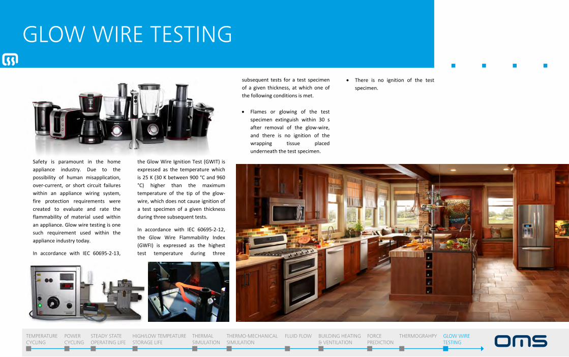
teMPeratUre cYcling
PoWer cYcling
SteaDY State oPerating life
high/loW teMPeatUre Storage life
therMal SiMUlation
therMo-Mechanical SiMUlation
flUiD floW bUilDing heating & ventilation
force PreDiction
therMograhPY gloW Wire teSting
gloW Wire teSting
GLOW WIRE TESTING
THERMAL CHARACTERIZATION & SERVICES FOLLOW THE RIGHGT LIGHT | 12
Safety is paramount in the home appliance industry. Due to the possibility of human misapplication, over-current, or short circuit failures within an appliance wiring system, fire protection requirements were created to evaluate and rate the flammability of material used within an appliance. Glow wire testing is one such requirement used within the appliance industry today.
In accordance with IEC 60695-2-13,
the Glow Wire Ignition Test (GWIT) is expressed as the temperature which is 25 K (30 K between 900 °C and 960 °C) higher than the maximum temperature of the tip of the glow-wire, which does not cause ignition of a test specimen of a given thickness during three subsequent tests.
In accordance with IEC 60695-2-12, the Glow Wire Flammability Index (GWFI) is expressed as the highest test temperature during three
subsequent tests for a test specimen of a given thickness, at which one of the following conditions is met. • Flames or glowing of the test
specimen extinguish within 30 s after removal of the glow-wire, and there is no ignition of the wrapping tissue placed underneath the test specimen.
• There is no ignition of the test specimen.

nanotechnologY

nanotechnologY
nano led module
nanoStructureS in optical solutions by omS
the independent research department
in partnership with a nanotechnology company from the foreign country
Develops and tests first samples
new opportunities for designing a new generation of luminaires

concePt anD DeSign

Design Plus 2014
team and their reSponSibilitieS
cooperation with external designers on regional and international level
creation of concepts according international lighting design based
on sketches and renderings
System level Design – research for the best solution (shape, technology)
creation of mockups with scaled clay models
Designing luminaires for oMS elite branD – high end luminaires
with special design and technical parameters
SoftWare and toolS Which are uSed by omS deSignerS
rhinozeros 3D – 3D modeling software
vraY – photorealistic rendering module for rhinozeros 3D
adobe cS and via 3D to create photorealistic animations and visualizations
concePt anD DeSign
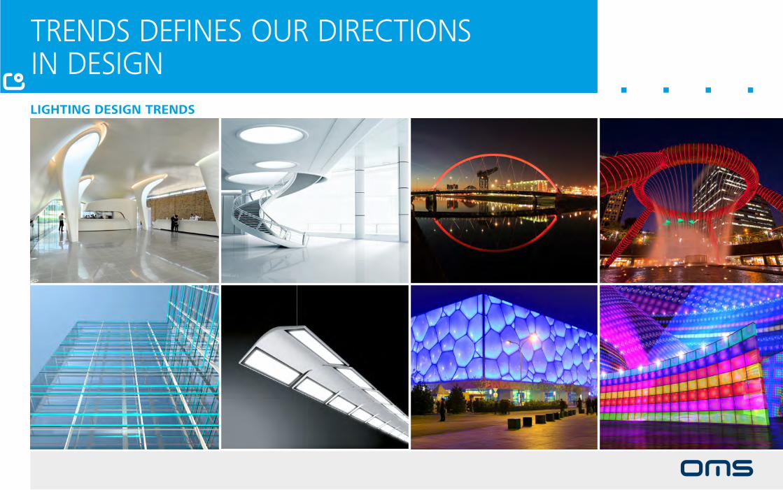
trenDS DefineS oUr DirectionS in DeSignlighting deSign trendS

trenDS DefineS oUr DirectionS in DeSigndeSign trendS

End cap detail
Suspended one version
Suspended double version
Suspended proposal
Upper detail
Bottom detail
Suspended
Semi-recessed a1
Recessed
Recessed
Semi-recessed a2
Shape/module variations
Vacuum formed covers
Shape/module variations
Vacuum formed covers
Shape/module variations
Vacuum formed covers
Shape/module variations
Vacuum formed covers
Shape/module variations
Vacuum formed covers
concePt anD DeSign

Mechanical DePartMent

With Which SoftWare iS omS developing luminaireS
3D caD software catia v5r20 from DaSSaUlt
Wiring module
generative sheet design module
generative shape design module
SMarteaM – professional PDM/PlM system documentation management
neW product development
fully computer supported process system
changing luminaire specs according customer needs
Direct connection to prototype workshop
optimization of existing products – unifications – platform based
Mechanical DePartMent

cuStomized SolutionS
Dedicated team for customer demanded luminaires
Direct connected to our porototype workshop – fast sampling
interface for electronic and optic design
Maintaining projects
Mechanical DePartMent
innovative SolutionS reQuire a different approach
INNOVATIVE SOLUTIONSREQUIRE A DIFFERENT APPROACH
LIGHTINGINNOVATIONCENTER
INDEPENDENTELECTRONIC
STANDARDHEATSINK
LEDMODULE
SECONDARYOPTIC
• REDUCTION OF HEATSINK SIZE BASED ON
- NEW MATERIALS
- NEW TECHNOLOGY
• INTELIGENT ELECTRONICS ON BOARD
• OPTIMALIZED OUTPUT LEVELS
• HIGH EFFICIENT CONSTATNT VOLTAGE APPROACH
• CONTROLABILITY FOR TW AND RGB
• CUSTOMER FRIENDLY USER INTERFACE
• OPTIC STRUCTURE DIRECTLY APPLIED
• NO NEED FOR SECONDARY OPTICS
• CUSTOMER SPECIFIC LIGHT DISTRIBUTION
• HIGH EFFICIENT FOR MAXIMUM LOR
THERMAL DESIGN
ELECTRONIC SOLUTION
NANO-OPTICS

SUPPlY chain ManageMent

SUPPlY chain ManageMent
Spend & Supply Strategy
logiSticS
ServiceS
indirect materialS
direct materialS
Sup
po
rtin
g developm
en
tpr
op
oSing effective Solu
tio
nS
supply chain managementStrategic purchaSin
g
ma
nu
facturability
cuSt
omer
Support
pro
ject
cal
culationS Strategic cooperatio
n
technology eva
lua
tio
n
th
e beSt
p
ro
du
ct
technical purchaser
electrical purchaser
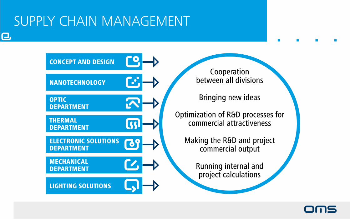
SUPPlY chain ManageMent
LigHTiNg soLUTioNs
MEcHANicAL DEPARTMENT
ELEcTRoNic soLUTioNs DEPARTMENT
THERMAL DEPARTMENT
oPTic DEPARTMENT
NANoTEcHNoLogy
Cooperation between all divisions
Bringing new ideas
Optimization of R&D processes for commercial attractiveness
Making the R&D and project commercial output
Running internal and project calculations
coNcEPT AND DEsigN

Founded: 1995
Liability Limited Company (Ltd.)
number of employees: 979
export: 98%
Distribution: 122 countries
area: 92 600 m²
Covered area: 33 550 m²
Production area: 16 000 m²
area of Warehouses: 12 000 m²
administrative area: 6 550 m²
Lighting innovation Centre


4 Software installation
4.1 Software installation requirementsBefore software installation and setup you will need: • Knowledge about how to perform the IP configuration of your PC, Android or iOS device • Knowledge about the IP configuration used for your LAN • Knowledge about the configuration of your DALI installation
4.2 PC application for Windows NT / XP / 2000 / Vista / 7 / 8
4.2.1 Graphical User Interface overview
Refresh buttonReloads the list of controls and application settings
and reconnects the device
Connection / password settings buttonOpens the IP / port / password
settings window (see 4.2.3 TCP/IP, port and password settings)
Control management buttonOpens the control management tool
(see 5.4 Control management)
Firmware update buttonStarts the device firmware update (see 5.6 Firmware update)
List of individual luminaire controls
List of timer controls
List of scene controls
List of group controls
TunableWhite slider (see 5.3 Control types)
Broadcast dimming slider (see 5.3 Control types)
RGB slider (see 5.3 Control types)
On / off button (see 5.3 Control types)
Status bar Shows information about last connection status
Figure 3: PC application Graphical User Interface7
2 IntroductionDEEBRIDGE is a solution comprising an Ethernet to DALI bridge device (Figure 1) and easily operated user interface application. This solution enables intuitive control of luminaires within a DALI installation via an Ethernet network using a PC, tablet or smartphone. The software runs on Windows, Android and iOS.
2.1 Features • An intuitive and user friendly Graphical User Interface (GUI)
• Broadens the possibilities of lighting control
• Enables the real-time control of brightness, colour temperature and RGB output
• The PC application enables date and time functions
2.2 Overview of the deviceThe device comes housed in a standard 2U sized DIN box which allows for installation on electrical switchboards. It is powered by an external 12 V DC Power Source Unit (not standardly supplied with the device but available on request). Figure 2 depicts a simplified connection schematic of the Ethernet to DALI bridge device.
Figure 1: Overview of the Ethernet to DALI bridge device Figure 2: Simplified connection schematic
2.3 Default settingsInitial Ethernet to DALI bridge device TCP/IP and port configuration settings: TCP/IP address: 192.168.1.252 Port: 8421 Default web configuration settings: Username: admin Password: admin
How to change the Ethernet to DALI bridge device IP address and port is covered in 3 Hardware Installation.
DALI -
DALI +
12 V DC
Power status indicatorDALI status indicator
Device status indicator
RESET button
RJ45 Ethernet connector
12 V DCPowerSupplyUnit
+ -
L PE N
LAN 230 V AC
Existing self-powered DALI installation
4
tunable White control intelligent leD module central Power Source DeebriDge
PB1 PB2

thanK yOu
HEad OffiCE OMS, spol. s r. o., 906 02 Dojč 419, Slovak Republic [email protected] oms.lighting
´FOLLOW THE RIGHT LIGHT´