lecture7 ee720 eq intro txeq
DESCRIPTION
ECEN720: High-Speed Links Circuits and Systems Spring 2013Lecture 7: Equalization Introduction & TX FIR EqTRANSCRIPT

Sam Palermo Analog & Mixed-Signal Center
Texas A&M University
ECEN720: High-Speed Links Circuits and Systems
Spring 2013
Lecture 7: Equalization Introduction & TX FIR Eq
Announcements
• Exam 1 is March 6 • 4:10-5:35PM (10 extra minutes) • Closed book w/ one standard note sheet • 8.5”x11” front & back • Bring your calculator • Covers material through lecture 6 • Previous years’ exam 1s are posted on the website for reference
• Special seminar this Friday • 10:20AM, Zachry 119C • Karl Muth –TI • “Model Based Systems Engineering for High Speed Optical Links” • Attendance = 10pts extra credit distributed on your HW/Lab score
2

Agenda
• Equalization theory and circuits • Equalization overview • Equalization implementations
• TX FIR • RX FIR • RX CTLE • RX DFE
• TX FIR Equalization • FIR filter in time and frequency domain • MMSE Coefficient Selection • Circuit Topologies
• Equalization overview paper posted on website
3
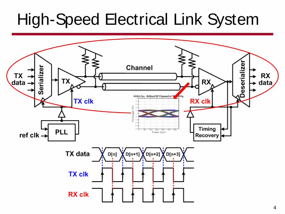
High-Speed Electrical Link System
4

Link with Equalization
5
Seria
lizer
DTX[N:0]
TX Clk Generation
(PLL)
TX FIR Equalization
RX Clk Recovery
(CDR/Fwd Clk)
Σ
RX CTLE + DFE Equalization
Des
eria
lizer
DRX[N:0]
Channel
f

6
Channel Performance Impact
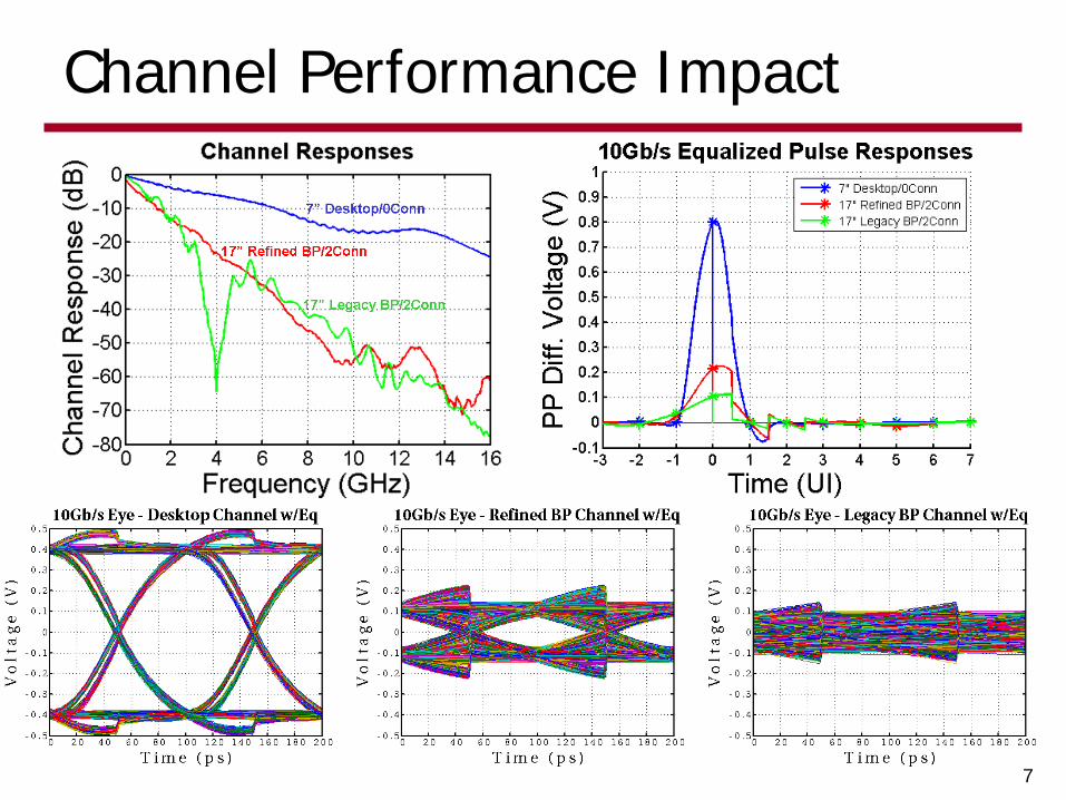
7
Channel Performance Impact

Channel Equalization
8
• Equalization goal is to flatten the frequency response out to the Nyquist Frequency and remove time-domain ISI

TX FIR Equalization
• TX FIR filter pre-distorts transmitted pulse in order to invert channel distortion at the cost of attenuated transmit signal (de-emphasis)
9
L
L L
L
L
L
L
L
L
1x 4x 2x 1x
1/4 1 1/2 1/4IDACs&
BiasControl
sgn-1 sgn0 sgn1 sgn2
50Ω
Out-P
Out-N
4:2MUX
2
2
2
21
D0
D1
D2
D3
VDDA=1.2VVDD=1.0V
VDDIO=1.0V
VDDA=1.2V
1
1
1
C2 (5GHz)From on-chip PLL
2
(2.5
Gb/
s)
(10Gb/s)
(5Gb/s)
ESD
L
L L
L
L
L
L
L
L
LL
LL LL
LL
LL
LL
LL
LL
LL
1x 4x 2x 1x
1/4 1 1/2 1/4IDACs&
BiasControl
sgn-1 sgn0 sgn1 sgn2
50Ω
Out-P
Out-N
4:2MUX
2
2
2
21
D0
D1
D2
D3
VDDA=1.2VVDD=1.0V
VDDIO=1.0V
VDDA=1.2V
1
1
1
C2 (5GHz)From on-chip PLL
2
(2.5
Gb/
s)
(10Gb/s)
(5Gb/s)
ESD
( ) ( ) ( ) ( ) ( )[ ]
−+−++= − 2
21010 2101TERM
outRDIDIDIDIV
“A Low Power 10Gb/s Serial Link Transmitter in 90-nm CMOS,” A. Rylyakov et al., CSICS 2005
I-1 I0 I1 I2
D(1) D(0) D(-1) D(-2)

6Gb/s TX FIR Equalization Example
• Pros • Simple to implement • Can cancel ISI in pre-
cursor and beyond filter span
• Doesn’t amplify noise • Can achieve 5-6bit
resolution
• Cons • Attenuates low
frequency content due to peak-power limitation
• Need a “back-channel” to tune filter taps
10
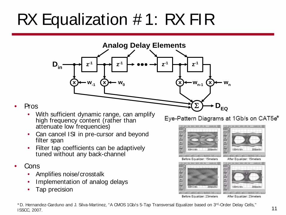
RX Equalization #1: RX FIR
• Pros • With sufficient dynamic range, can amplify
high frequency content (rather than attenuate low frequencies)
• Can cancel ISI in pre-cursor and beyond filter span
• Filter tap coefficients can be adaptively tuned without any back-channel
• Cons • Amplifies noise/crosstalk • Implementation of analog delays • Tap precision
11
w-1
z-1
x w0
z-1
x
z-1
x wn-1
z-1
wnx
Σ DEQ
Din
Analog Delay Elements
*
*D. Hernandez-Garduno and J. Silva-Martinez, “A CMOS 1Gb/s 5-Tap Transversal Equalizer based on 3rd-Order Delay Cells," ISSCC, 2007.

RX Equalization #2: RX CTLE
12
Din- Din+
Vo-Vo+
• Pros • Provides gain and
equalization with low power and area overhead
• Can cancel both pre-cursor and long-tail ISI
• Cons • Generally limited to 1st
order compensation • Amplifies noise/crosstalk • PVT sensitivity • Can be hard to tune
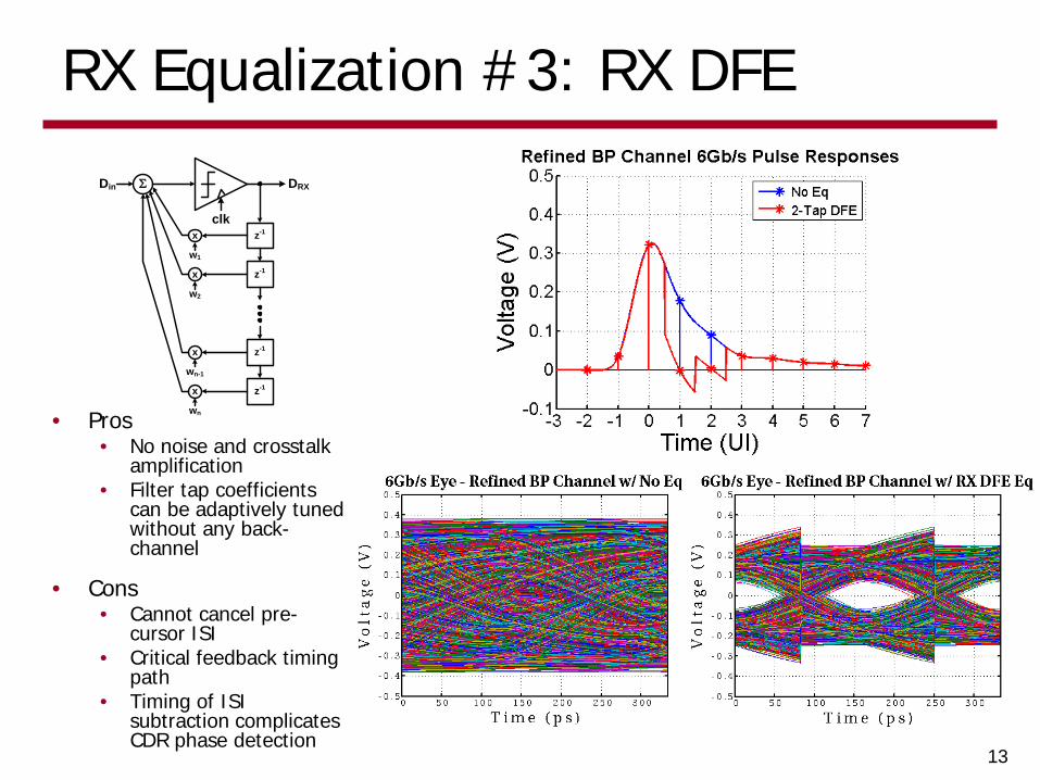
RX Equalization #3: RX DFE
13
z-1clk
Σ
x
w1
z-1x
w2
z-1x
wn-1
z-1x
wn
Din DRX
• Pros • No noise and crosstalk
amplification • Filter tap coefficients
can be adaptively tuned without any back-channel
• Cons • Cannot cancel pre-
cursor ISI • Critical feedback timing
path • Timing of ISI
subtraction complicates CDR phase detection

Equalization Effectiveness
• Some observations: • Big initial performance boost with 2-tap TX eq. • With only TX eq., not much difference between 2 to 4-tap • RX equalization, particularly DFE, allows for further performance
improvement • Caution – hard to build fast DFEs due to critical timing path
14
Incr
easi
ng
Equa
lizat
ion
Channel Responses

Link with Equalization
15
Seria
lizer
DTX[N:0]
TX Clk Generation
(PLL)
TX FIR Equalization
RX Clk Recovery
(CDR/Fwd Clk)
Σ
RX CTLE + DFE Equalization
Des
eria
lizer
DRX[N:0]
Channel
f

Channel Equalization
16
• Equalization goal is to flatten the frequency response out to the Nyquist Frequency and remove time-domain ISI
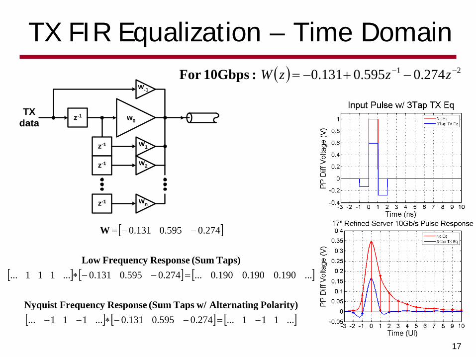
TX FIR Equalization – Time Domain
17
z-1
z-1
z-1
w-1
w0
w1
w2
TXdata
z-1 wn
( ) 21 274.0595.0131.0 −− −+−= zzzW :10GbpsFor
[ ]
[ ] [ ] [ ]
[ ] [ ] [ ]...111...274.0595.0131.0...111...
...190.0190.0190.0...274.0595.0131.0...111...
274.0595.0131.0
−=−−∗−−
=−−∗
−−=
Polarity) ng Alternatiw/ Taps (Sum Response FrequencyNyquist
Taps) (Sum Response Frequency Low
W

TX FIR Equalization – Freq. Domain
18
z-1
z-1
z-1
w-1
w0
w1
w2
TX data
z-1 wn
( ) 21 274.0595.0131.0 −− −+−= zzzW :10GbpsFor
( )( )ss
fTj fTjfTezzzzW
s πππ 2sin)2cos(
274.0595.0131.02
21
+==
−+−= −−
w/
( )( ) ( ) dBfWjz
f4.14190.001)0sin(0cos −⇒==⇒=+=
= 0 Response Frequency Low
( ) dBT
fWjz
Tf
s
s
01211)sin(cos
21
⇒−=
=⇒−=+=
=
ππ
Response FrequencyNyquist
• Equalizer has 14.4dB of frequency peaking • Attenuates DC at -14.4dB and passes Nyquist frequency at 0dB
Note: Ts=Tb=100ps
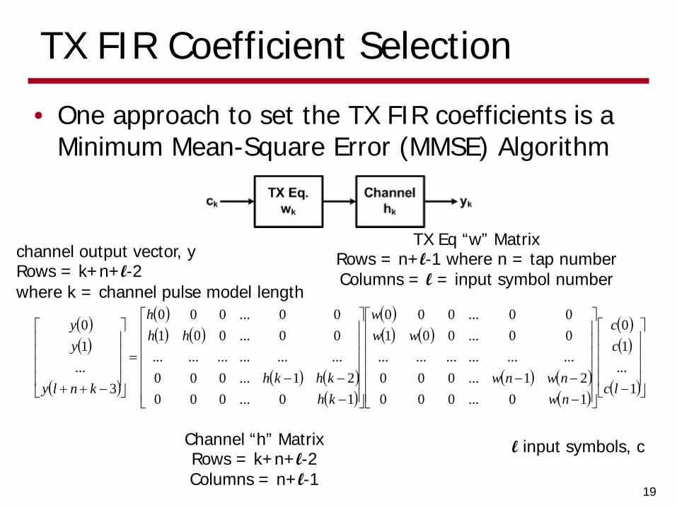
TX FIR Coefficient Selection
• One approach to set the TX FIR coefficients is a Minimum Mean-Square Error (MMSE) Algorithm
19
( )( )
( )
( )( ) ( )
( ) ( )( )
( )( ) ( )
( ) ( )( )
( )( )
( )
−
−−−
−−−
=
−++ 1...10
10...00021...000
..................00...00100...000
10...00021...000
..................00...00100...000
3...10
lc
cc
nwnwnw
www
khkhkh
hhh
knly
yy
l input symbols, c
channel output vector, y Rows = k+n+l-2 where k = channel pulse model length
TX Eq “w” Matrix Rows = n+l-1 where n = tap number Columns = l = input symbol number
Channel “h” Matrix Rows = k+n+l-2 Columns = n+l-1
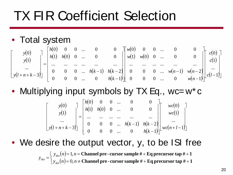
TX FIR Coefficient Selection
• Multiplying input symbols by TX Eq., wc=w*c
20
( )( )
( )
( )( ) ( )
( ) ( )( )
( )( ) ( )
( ) ( )( )
( )( )
( )
−
−−−
−−−
=
−++ 1...10
10...00021...000
..................00...00100...000
10...00021...000
..................00...00100...000
3...10
lc
cc
nwnwnw
www
khkhkh
hhh
knly
yy
• Total system
( )( )
( )
( )( ) ( )
( ) ( )( )
( )( )
( )
−+
−−−
=
−++ 1...
10
10...00021...000
..................00...00100...000
3...10
lnwc
wcwc
khkhkh
hhh
knly
yy
• We desire the output vector, y, to be ISI free ( )( )
++≠=++==
=1 # tapprecursor Eq # samplecursor -pre Channel1 # tapprecursor Eq # samplecursor -pre Channel
nnynny
ydes
desdes ,0
,1
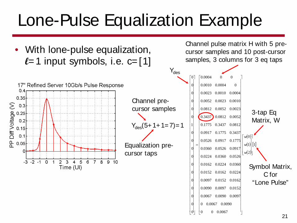
Lone-Pulse Equalization Example
21
• With lone-pulse equalization, l=1 input symbols, i.e. c=[1]
( )( )( )
[ ]12
1
0
0.0067 0 0
0.0090 0.0067 0
0.0097 0.0090 0.0067
0.0152 0.0097 0.0090
0.0162 0.0152 0.0097
0.0224 0.0162 0.0152
0.0360 0.0224 0.0162
0.0526 0.0360 0.0224
0.0917 0.0526 0.0360
0.1775 0.0917 0.0526
0.3437 0.1775 0.0917
0.0812 0.3437 0.1775
0.0052 0.0812 0.3437
0.0023 0.0052 0.0812
0.0010 0.0023 0.0052
0.0004 0.0010 0.0023
0 0.0004 0.0010
0 0 0.0004
0
0
0
0
0
0
0
0
0
0
0
1
0
0
0
0
0
0
=
w
w
w
Ydes
Channel pulse matrix H with 5 pre-cursor samples and 10 post-cursor samples, 3 columns for 3 eq taps
3-tap Eq Matrix, W
Symbol Matrix, C for
“Lone Pulse”
Ydes(5+1+1=7)=1
Channel pre-cursor samples
Equalization pre-cursor taps

TX FIR Coefficient Selection
• Differentiating this w.r.t. tap matrix taps to find taps which yield minimum error norm2
22
input pulse with desdesCdes YHWYHWYYE −=−=−=• We can calculate the error w.r.t. a desired output
HYHHW
HYHHWEdWd
Tdes
TT
Tdes
TT
=
=−= 0222
• Solving for optimum TX Eq taps, W ( ) desTT
ls YHHHW 1−=
desT
desT
desTT YYHWYHWHWE +−= 22
• Computing the error matrix norm2
• This will yield a W matrix to produce a value of “1” at the output cursor, i.e. an FIR filter with gain • Need to normalize by the total abs(tap) sum for TX FIR realization
( ) ( )( )∑
=
= n
ils
lslsnorm
nW
nWnW
1

TX FIR Tap Resolution
23
• Using the above MMSE algorithm for the Refined Server Channel at 10Gb/s
( )[ ]
[ ]274.0595.0131.011
274.0595.0131.0 21
−−
−+−= −−
postmainprezzzW
• Generally, TX DAC resolution is limited to between 4 to 6bits
• Mapping these equalization coefficients with this resolution may impact performance
=⇒
=
0.2745-
0.5949
0.1307-
1.7184-
3.7245
0.8180-6.2609by gnormalizin
lsnormls WW
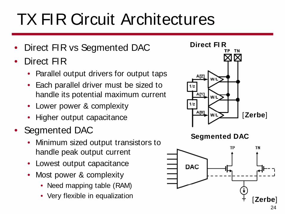
TX FIR Circuit Architectures
• Direct FIR vs Segmented DAC • Direct FIR
• Parallel output drivers for output taps • Each parallel driver must be sized to
handle its potential maximum current • Lower power & complexity • Higher output capacitance
• Segmented DAC • Minimum sized output transistors to
handle peak output current • Lowest output capacitance • Most power & complexity
• Need mapping table (RAM) • Very flexible in equalization
24
Segmented DAC
Direct FIR
[Zerbe]
[Zerbe]
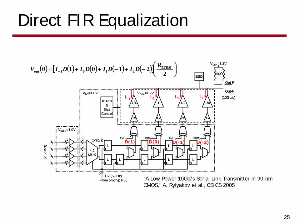
Direct FIR Equalization
25
L
L L
L
L
L
L
L
L
1x 4x 2x 1x
1/4 1 1/2 1/4IDACs&
BiasControl
sgn-1 sgn0 sgn1 sgn2
50Ω
Out-P
Out-N
4:2MUX
2
2
2
21
D0
D1
D2
D3
VDDA=1.2VVDD=1.0V
VDDIO=1.0V
VDDA=1.2V
1
1
1
C2 (5GHz)From on-chip PLL
2
(2.5
Gb/
s)
(10Gb/s)
(5Gb/s)
ESD
L
L L
L
L
L
L
L
L
LL
LL LL
LL
LL
LL
LL
LL
LL
1x 4x 2x 1x
1/4 1 1/2 1/4IDACs&
BiasControl
sgn-1 sgn0 sgn1 sgn2
50Ω
Out-P
Out-N
4:2MUX
2
2
2
21
D0
D1
D2
D3
VDDA=1.2VVDD=1.0V
VDDIO=1.0V
VDDA=1.2V
1
1
1
C2 (5GHz)From on-chip PLL
2
(2.5
Gb/
s)
(10Gb/s)
(5Gb/s)
ESD
( ) ( ) ( ) ( ) ( )[ ]
−+−++= − 2
21010 2101TERM
outRDIDIDIDIV
“A Low Power 10Gb/s Serial Link Transmitter in 90-nm CMOS,” A. Rylyakov et al., CSICS 2005
I-1 I0 I1 I2
D(1) D(0) D(-1) D(-2)
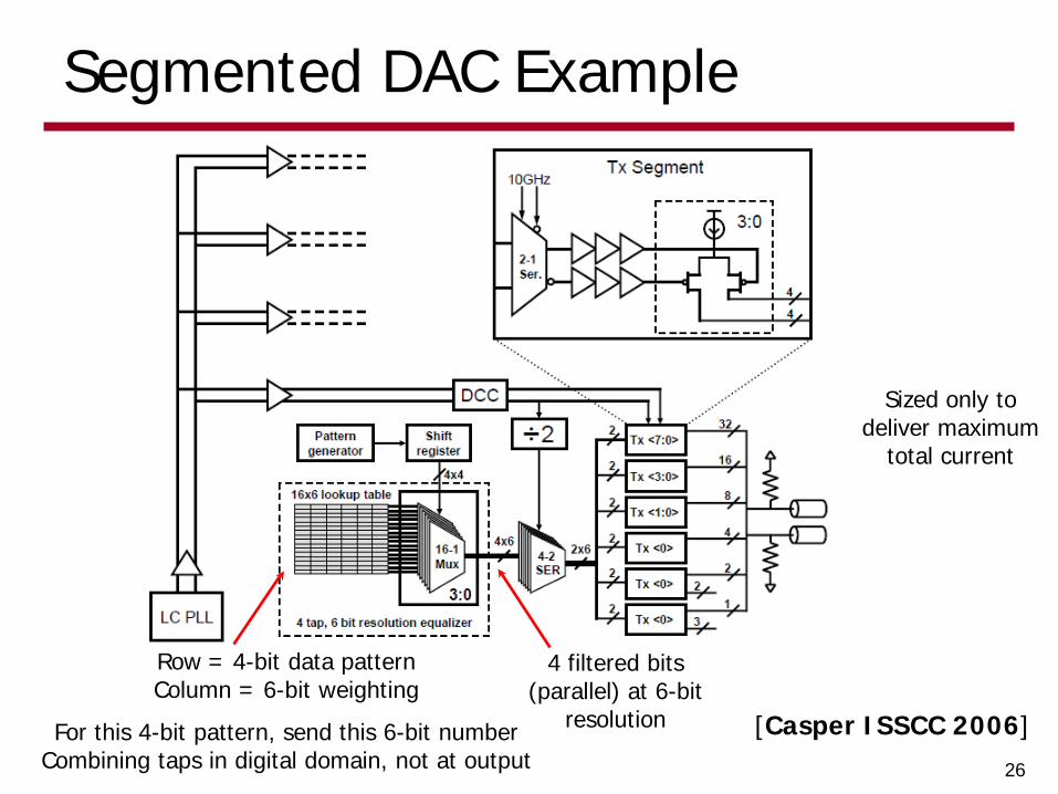
Segmented DAC Example
26
[Casper ISSCC 2006]
Row = 4-bit data pattern Column = 6-bit weighting
For this 4-bit pattern, send this 6-bit number Combining taps in digital domain, not at output
4 filtered bits (parallel) at 6-bit
resolution
Sized only to deliver maximum
total current

Next Time
• RX FIR • RX CTLE • RX DFE • Alternate/Future Approaches
27