lecture #14 implementation of finite‐ difference …emlab.utep.edu/ee5390cem/lecture 14 -- fdfd...
TRANSCRIPT

11/5/2017
1
Lecture 14 Slide 1
EE 5337
Computational Electromagnetics (CEM)
Lecture #14
Implementation of Finite‐Difference Frequency‐Domain These notes may contain copyrighted material obtained under fair use rules. Distribution of these materials is strictly prohibited
InstructorDr. Raymond Rumpf(915) 747‐[email protected]
• Basic flow of FDFD
• 2× grid technique
• Calculating grid parameters
• Constructing your device on the grid
• Walkthrough of the FDFD algorithm
• Examples for benchmarking
Outline
Lecture 14 Slide 2

11/5/2017
2
Lecture 14 Slide 3
Basic Flow of FDFD
Lecture 14 Slide 4
Block Diagram of FDFD Implementation
Dashboard
Calculate Grid
Build Device on Grid
Incorporate PML
Calculate Wave Vector Components
Build Wave Matrix A
Compute Source
Solve Ax = b
Post‐Process
Source, device, learn, and grid
Nx, Ny, dx, dy, xa, ya
All hard‐coded numbers. No work.No hard‐coded numbers. All work.
,inc ,inc ,ref ,trn, , , , x y x y yk k k m k m k m
E j H
H j E
Ax 0
src b QA AQ f
RDE, TDE, REF, TRN, CON
FDFD

11/5/2017
3
Lecture 14 Slide 5
Detailed FDFD Algorithm
1. Construct FDFD Problema. Define your problemb. Calculate the grid parametersc. Assign materials to the grid to
build ER2 and UR2 arrays
2. Handle PML and Materialsa. Compute sx and syb. Incorporate into r and r
c. Overlay onto 1× grids
3. Compute Wave Vector Componentsa. Identify materials in reflected and
transmitted regions: ref, trn, ref, trn, nref, ntrn
b. Compute incident wave vector: kincc. Compute transverse wave vector
expansion: kx,md. Compute ky,ref and ky,trn
4. Construct Aa. Construct diagonal materials
matricesb. Compute derivative matricesc. Compute A
5. Compute Source Vector, ba. compute source field fsrcb. compute Qc. compute source vector b
6. Solve Matrix Problem: e = A‐1b;
7. Post Process Dataa. Extract Eref and Etrnb. Remove phase tiltc. FFT the fieldsd. Compute diffraction efficienciese. Compute reflectance & transmittance
f. Compute conservation of power
Lecture 14 Slide 6
2× Grid Technique

11/5/2017
4
Lecture 14 Slide 7
What is the 2× Grid Technique? (1 of 2)
DeviceNxNydxdy
1× Grid
Device on 1× Grid
VERY DIFFICULT STEP !!
This is the traditional approach for building devices on a Yee grid.
It is very tedious and cumbersome to determine which field components reside in which material.
Lecture 14 Slide 8
What is the 2× Grid Technique? (2 of 2)
DeviceNxNydxdy
1× Grid
Device on 1× Grid
Nx2 = 2*NxNy2 = 2*Nydx2 = dx/2dy2 = dy/2
2× Grid Device on 2× Grid
easy
easy
easy
The 2× grid technique simplifies how devices are built into the permittivity and permeability arrays.

11/5/2017
5
Diagonalize Materials
Parse to 1× Grid
Lecture 14 Slide 9
Block Diagram of FDFD With 2× Grid
Dashboard
Calculate Grid
Build Device on 2× Grid
Incorporate PML on 2× Grid
Calculate Wave Vector Components
Build Wave Matrix A
Compute Source
Solve Ax = b
Post‐Process
Source, device, learn, and grid
Nx, Ny, dx, dy, xa, ya
All hard‐coded numbers. No work.
No hard‐coded numbers. All work.
,inc ,inc ,ref ,trn, , , , x y x y yk k k m k m k m
1 1
1 1
h e h eE x yy x y xx y zz
e h e hH x yy x y xx y zz
A D μ D D μ D ε
A D ε D D ε D μ
src b QA AQ f
RDE, TDE, REF, TRN, CON
ER2UR2
2Grid Only Used Here
Build Derivate Matrices
, , and e e h hx y x y D D D D
FDFD
Lecture 14 Slide 10
Recall the Yee Grid
xy
z
xEyE
zE
xHyH
zH
3D Yee Grid2D Yee Grids1D Yee Grid
zE
xHyH
xy
xy
zH yExE
Ez Mode
Hz Mode
z
xE
yH
yExH
Ey Mode
Ex Mode
z

11/5/2017
6
Lecture 14 Slide 11
4×4 Yee Grids
H Mode
E Mode
Lecture 14 Slide 12
Simplified Representation of E‐Field Components
• The field components are physically positioned at the edges of the cell.
• The simplified representation shows the fields inside the cells to convey more clearly which cell they are in.

11/5/2017
7
Lecture 14 Slide 13
Simplified Representation of E‐Field Components
• The field components are physically positioned at the edges of the cell.
• The simplified representation shows the fields inside the cells to convey more clearly which cell they are in.
Lecture 14 Slide 14
The 2× Grid
i
j
The Conventional 1× Grid
y
x i
j
Due to the staggered nature of the Yee grid,
we are effectively getting twice the resolution.
i
j
It now makes sense to talk about a grid that is at twice the resolution,
the “2× grid.”
The 2× grid concept is useful because we can create devices (or PMLs) on the 2× grid without having to think about where the different field components are located. In a second step, we can easily pull off the values from the 2× grid where they exist for a particular field component.
11/5/2017
8
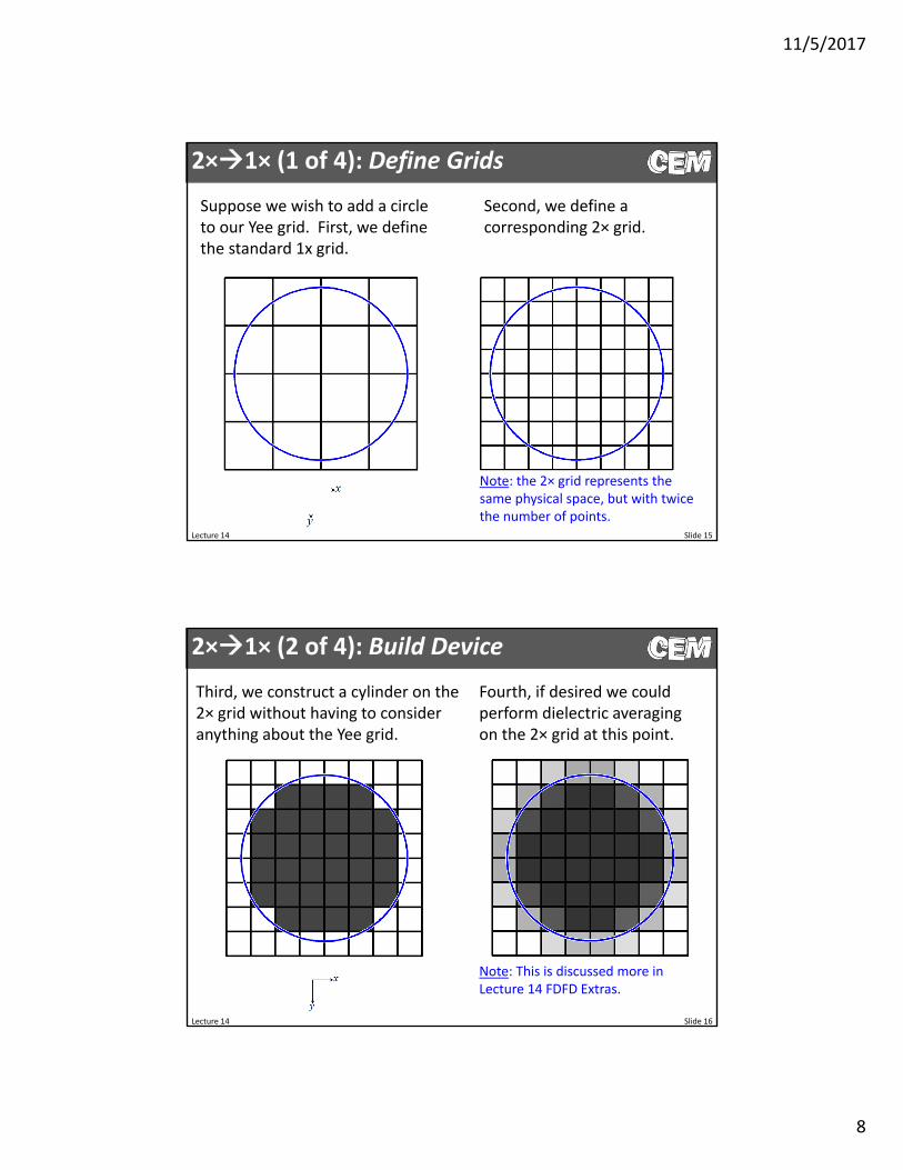
Lecture 14 Slide 15
2×1× (1 of 4): Define Grids
Suppose we wish to add a circle to our Yee grid. First, we define the standard 1x grid.
Second, we define a corresponding 2× grid.
Note: the 2× grid represents the same physical space, but with twice the number of points.
Lecture 14 Slide 16
2×1× (2 of 4): Build Device
Third, we construct a cylinder on the 2× grid without having to consider anything about the Yee grid.
Fourth, if desired we could perform dielectric averaging on the 2× grid at this point.
Note: This is discussed more in Lecture 14 FDFD Extras.
11/5/2017
9
Lecture 14 Slide 17
2×1× (3 of 4): Recall Field Staggering
Recall the relation between the 2× and 1× grids as well as the location of the field components.
Lecture 14 Slide 18
2×1× (4 of 4): Parse to 1× Grid

11/5/2017
10
Lecture 14 Slide 19
Extract ERxx from ER2
ERxx = ER2(2:2:Nx2,1:2:Ny2)
Lecture 14 Slide 20
Extract ERyy from ER2
ERyy = ER2(1:2:Nx2,2:2:Ny2)

11/5/2017
11
Lecture 14 Slide 21
Extract ERzz from ER2
ERzz = ER2(1:2:Nx2,1:2:Ny2)
Lecture 14 Slide 22
Extract URxx from UR2
URxx = UR2(1:2:Nx2,2:2:Ny2)

11/5/2017
12
Lecture 14 Slide 23
Extract URyy from UR2
URyy = UR2(2:2:Nx2,1:2:Ny2)
Lecture 14 Slide 24
Extract URzz from UR2
URzz = UR2(2:2:Nx2,2:2:Ny2)

11/5/2017
13
Lecture 14 Slide 25
MATLAB Code for Parsing Onto 1× Grid
ERxx = ER2(2:2:Nx2,1:2:Ny2,1:2:Nz2);ERyy = ER2(1:2:Nx2,2:2:Ny2,1:2:Nz2);ERzz = ER2(1:2:Nx2,1:2:Ny2,2:2:Nz2);
URxx = UR2(1:2:Nx2,2:2:Ny2,2:2:Nz2);URyy = UR2(2:2:Nx2,1:2:Ny2,2:2:Nz2);URzz = UR2(2:2:Nx2,2:2:Ny2,1:2:Nz2);
EzMode
ERzz = ER2(1:2:Nx2,1:2:Ny2);
URxx = UR2(1:2:Nx2,2:2:Ny2);URyy = UR2(2:2:Nx2,1:2:Ny2);
HzMode
ERxx = ER2(2:2:Nx2,1:2:Ny2);ERyy = ER2(1:2:Nx2,2:2:Ny2);
URzz = UR2(2:2:Nx2,2:2:Ny2);
Lecture 14 Slide 26
Calculating the Grid Parameters

11/5/2017
14
Lecture 14 Slide 27
Model Construction
periodic boundary
Dirichlet boundary
PML
PML
perio
dic b
oundary
Dirichlet boundary
20 cells
20 cells
Lecture 6 Slide 28
Consideration #1: Wavelength 0The grid resolution must be sufficient to resolve the shortest wavelength.
N Comments
10 to 20 Low contrast dielectrics
20 to 30 High contrast dielectrics
40 to 60 Most metallic structures
100 to 200 Plasmonic devices
0min
min
max ,n x y
min[0] is the shortest wavelength of interest in your simulation. max[n(x,y)] is the largest refractive index found anywhere in the grid.
First, you must determine the smallest wavelength:
min 10NN
Second, you resolve the wave with at least 10 cells.
1 point

11/5/2017
15
Lecture 6 Slide 29
Consideration #2: Mechanical Features
The grid resolution must be sufficient to resolve the smallest mechanical features of the device.
1dN 4dN 1dN 1dN
Unit cell of a diamond lattice
mind
mind
First, you must determine the smallest feature:
min 1d dd
dN
N
Second, you must divide this by 1 to 4.
Lecture 14 Slide 30
Calculating the Initial Grid Resolution
x
2. We must resolve the minimum structural dimension.
min 1d dd
NN
We proceed with the smallest of the above quantities to be our initial grid resolution
min ,x y d
y
1. We must resolve the minimum wavelength.
0min max , 10
n x yN
N
Note: If you are performing a parameter sweep over frequency or wavelength, min(0) is the shortest wavelength in the sweep.

11/5/2017
16
Lecture 14 Slide 31
Resolving Critical Dimensions (1 of 3)
We have not yet considered the actual dimensions of the device we wish to simulate.
This means we likely cannot resolve the exact dimensions of a device.
Not an exact fit.We cannot fill a fraction of a cell.
x
yd
Suppose we wish to place a device of length d onto a grid.
Lecture 14 Slide 32
Resolving Critical Dimensions (2 of 3)
To fix this, we first calculate how many cells N are needed to resolve the most important dimension. In this case, let this be d.
x
yd
x
dN
10.5 cellsN
Second, we determine how many cells we wish to exactly resolve d. We do this by rounding N up to the nearest integer.
ceilx
dN
11 cellsN

11/5/2017
17
Lecture 14 Slide 33
Resolving Critical Dimensions (3 of 3)
Third, we adjust the value of x to represent the dimension d exactly.
x
yd
x
d
N
11 cellsN
We call this step “snapping” the grid to a critical dimension.
Unfortunately, using a uniform grid, we can only do this for one dimension per axis.
Lecture 14 Slide 34
“Snap” Grid to Critical Dimensions
Decide what dimensions along each axis are critical.
Compute how many grid cells comprise dx and dy and round UP.
ceil
ceil
x x x
y y y
M d
M d
Adjust grid resolution to fit these critical dimensions in grid EXACTLY.
Typically this is a lattice constant or grating period along x Typically this is a film thickness or grating depth along y
x x x
y y y
d M
d M
initial grid
critical dim
ensio
n
adjusted
grid
critical dim
ensio
n
and x yd d
We will drop the prime symbol ‘ from x and y.

11/5/2017
18
Lecture 14 Slide 35
Compute Total Grid Size
x
y
yN
xN
• Don’t forget to add cells for PML!
• Must often add “space” between PML and device.
PML SPACE2 2
xx
x
yy
y
N
N N N
Problem Space
Spacer Region
Spacer Region
PML
PML
Note: This is particularly important when modeling devices with large evanescent fields.
maxSPACE
buff
ceily
Nn
Easiest to make Nx odd.Reason discussed later.
Lecture 14 Slide 36
Compute 2× Grid Parameters
1× Grid 2× Grid
Nx2 = 2*Nx; dx2 = dx/2;Ny2 = 2*Ny; dy2 = dy/2;

11/5/2017
19
Lecture 14 Slide 37
Constructing a Device on the Grid
Lecture 14 Slide 38
Reducing 3D Problems to 2D
x
y
z
Representation on a Cartesian grid
11/5/2017
20
Lecture 14 Slide 39
Averaging At the Edges
Direct Smoothed
Lecture 14 Slide 40
Building Rectangular Structures
For rectangular structures, considering calculating start and stop indices.
% BUILD DEVICEER2 = er1*ones(Nx2,Ny2); %fill everywhere with er1ER2(nx1:nx2,ny1:ny2) = er; %add tooth 1ER2(nx5:nx6,ny1:ny2) = er; %add tooth 2ER2(:,ny3:ny4) = er; %add substrateER2(:,ny4+1:Ny2) = er2; %fill transmission region
Be very careful with how many points on the grid you fill in!
ny2 = ny1 + round(d/dy2) – 1;
Without subtracting 1 here, filling in ny1to ny2 would include an extra cell. This can introduce error into your results.
nx1
ny1
nx2
nx3
nx4
nx5
ny2ny3ny4
nx6
1rr
2r
d

11/5/2017
21
Lecture 14 Slide 41
Oh Yeah, Metals!
Perfect Electric Conductors
10000r
1 1
00 0 1 0 0 m
M M
E f
E
E f
or
Include Tangential Fields at Boundary (TM modes!)
0mE
xy
zH yExE
Hz Mode
Bad placement of metals Good placement of metals
Lecture 14 Slide 42
Walkthrough of theFDFD Algorithm
11/5/2017
22
Lecture 14 Slide 43
Input to the FDFD Algorithm
The FDFD algorithm requires the following information:
•The materials on the 2× grid: ER2(nx,ny) and UR2(nx,ny)
•The grid resolution: dx and dy
•The size of the PML on the 1× grid: NYLO and NYHI
•The source wavelength, 0
•Angle of incidence,
•Mode/polarization: ‘E’ or ‘H’
Lecture 14 Slide 44
(1) Determine the Material Properties in the Reflected and Transmitted Regions
ER2(nx,ny) UR2(nx,ny)
refr
trnr
refr
trnr
If these parameters are not provided in the dashboard, or a dashboard does not exist, they can be pulled directly off of the grid.

11/5/2017
23
Lecture 14 Slide 45
(2) Compute the PML Parameters on 2× Grid
,xs x y ,ys x y
20 cells on Yee grid.40 cells on 2 grid.
20 cells on Yee grid.40 cells on 2 grid.
Lecture 14 Slide 46
(3) Incorporate the PML
0
0
r
r
E k H
H k E
0 0
0 0
0 0
y zxx
x
x zr yy
y
x yzz
z
s s
s
s s
s
s s
s
0 0
0 0
0 0
y zxx
x
x zr yy
y
x yzz
z
s s
s
s s
s
s s
s
We can incorporate the PML parameters into [μ] and [ε] as follows
For 2D simulations, sz = 1 and we have
yxx r
x
xyy r
y
zz x y r
s
s
s
s
s s
yxx r
x
xyy r
y
zz x y r
s
s
s
s
s s
Note: the PML is incorporated into the 2× grid.
% INCORPORATE PMLURxx = UR2./sx.*sy;URyy = UR2.*sx./sy;URzz = UR2.*sx.*sy;ERxx = ER2./sx.*sy;ERyy = ER2.*sx./sy;ERzz = ER2.*sx.*sy;

11/5/2017
24
Lecture 14 Slide 47
(4) Overlay Materials Onto 1× Grids
2X Grid
x
y
zE
zH
,x yH E
,y xH E
zz
zz
,xx yy
,yy xx
Field and materials assignments
zE
xHyH
xy
Ez Mode
xy
zH yExE
Hz Mode
I II
III IV
1× Grids
I II
III IV
% OVERLAY MATERIALS ONTO 1X GRIDURxx = URxx(1:2:Nx2,2:2:Ny2);URyy = URyy(2:2:Nx2,1:2:Ny2);URzz = URzz(2:2:Nx2,2:2:Ny2);ERxx = ERxx(2:2:Nx2,1:2:Ny2);ERyy = ERyy(1:2:Nx2,2:2:Ny2);ERzz = ERzz(1:2:Nx2,1:2:Ny2);
Lecture 14 Slide 48
(5) Compute the Wave Vector Terms
00
inc 0 ref
,inc
2 2,ref 0 ref
2 2,trn 0 trn
2
sin
cos
2x x
x
y x
y x
k
k k n
k m k m
k m k n k m
k m k n k m
This is a vector quantity
, 2, 1,0,1,2,m Nx points total.For proper symmetry, Nxshould be odd.
These equations come from the dispersion equation for the reflected and transmitted regions.
m = [-floor(Nx/2):floor(Nx/2)]';
Recall that there used to be a negative sign here. We are able to drop it as long as we also drop the negative sign when calculating diffraction efficiency.

11/5/2017
25
Lecture 14 Slide 49
(6) Construct Diagonal Materials Matrices
1 0
2
0
1 0
2
0
1 0
2
0
xx
xxxx
xx
yy
yyyy
yy
zz
zzzz
zz
N
N
N
ε
ε
ε
1 0
2
0
1 0
2
0
1 0
2
0
xx
xxxx
xx
yy
yyyy
yy
zz
zzzz
zz
N
N
N
μ
μ
μ
ERxx = diag(sparse(ERxx(:)));
Lecture 14 Slide 50
(7) Construct the Derivative Matrices
, , , and e e h hx y x y D D D D
[DEX,DEY,DHX,DHY] = yeeder(NGRID,k0*RES,BC,kinc/k0);
Don’t forget that we have normalized our parameters so you should use yeeder() as follows:
[DEX,DEY,DHX,DHY] = yeeder(NGRID,k0*RES,BC,kinc/k0);
Be sure this function uses sparse matrices from the very beginning.
A = sparse(M,M) – creates a sparse MM matrix of zeros.A = spdiags(b,d,A) – Adds array b to diagonal d in matrix A.
Frequency (or wavelength) information is incorporated into FDFD here

11/5/2017
26
Lecture 14 Slide 51
(8) Compute the Wave Matrix A
1 1h e h eE x yy x y xx y zz
A D μ D D μ D ε
1 1e h e hH x yy x y xx y zz
A D ε D D ε D μ
Mode
Mode
Lecture 14 Slide 52
(9) Compute the Source Field
src inc
,inc ,inc
, exp
exp x y
f x y jk r
j k x k y
inck
Don’t forget to make fsrc a column vector.
1 grid
The source has an amplitude of 1.0

11/5/2017
27
Lecture 14 Slide 53
(10) Compute the Scattered‐Field Masking Matrix, Q
total‐field
scattered‐field 1 1 1 1 1
1 1 1 1 1
1 1 1 1 1
1 1 1 1 1
0 0 0 0 0
0 0 0 0 0
0 0 0 0 0
0 0 0 0 0
0 0 0 0 0
0 0 0 0 0
1
1
0
0
0
Q
It is good practice to make the scattered‐field region at least one cell larger than the y‐low PML.
0
0
Reshape grid to 1D array and then diagonalize.
Q = diag(sparse(Q(:)));
Lecture 14 Slide 54
(11) Compute the source vector, b
src Af = b b QA AQ f

11/5/2017
28
Lecture 14 Slide 55
(12) Compute the Field f
1f = A b
Don’t forget to reshape() f from a column vector to a 2D grid after the calculation.
Aside
In MATLAB, f = A\b employs a direct LU decomposition to calculate f. This is very stable and robust, but a half‐full matrix is created so memory can explode for large problems.
Iterative solutions can be faster and require much less memory, but they are less stable and may never converge to a solution. Correcting these problems requires significant modification to the FDFD algorithm taught here.
Lecture 14 Slide 56
(13) Extract Transmitted and Reflected Fields
refE
trnE
SF
TF
The reflected field is extracted from inside the scattered‐field, but outside the PML.
The transmitted field is extracted from the grid after the device, but outside the PML.

11/5/2017
29
Lecture 14 Slide 57
(14) Remove the Phase Tilt
,i
, nc
nc
i
trn trn
ref ref
x
xjk
jk
x
xA
A x
x e
x
x E
E e
Recall Bloch’s theorem,
,i
, nc
nc
i
r
trn tr
ref
n
efx
x
k x
jk
j
xE
E x A x e
x A x e
This implies the transmitted and reflected fields have the following form
We remove the phase tilt to calculate the amplitude terms.
inc
inc
jk r
kE r A r e
Lecture 14 Slide 58
(15) Calculate the Complex Amplitudes of the Spatial Harmonics
ref ref
trn trn
FFT
FFT
S m A x
S m A x
Sref = flipud(fftshift(fft(Aref)))/Nx;Strn = flipud(fftshift(fft(Atrn)))/Nx;
Recall that the plane wave spectrum is the Fourier transform of the field.
We calculate the FFT of the field amplitude arrays.
Some FFT algorithms (like MATLAB) require that you divide by the number of points and shift after calculation.

11/5/2017
30
Lecture 14 Slide 59
(16) Calculate Diffraction Efficiencies
ref2 r,inc
ref incr,inc
ref2 r,inc
ref incr,inc
Re E Mode
Re
Re H Mode
Re
y
y
y
y
k mR m S m
k
k mR m U m
k
trn2 r,trn
trn incr,inc
trn2 r,trn
trn incr,inc
Re Mode
Re
Re Mode
Re
y
y
y
y
kT m S m E
k
kT m U m H
k
The source wave was given unit amplitude so2
inc 1S
The diffraction efficiencies of the reflected modes are then
The diffraction efficiencies of the transmitted modes are then
Note: these equations assume that . inc 1S
Recall that there used to be a negative sign here. We dropped it because we also dropped the sign when calculating . ,refyk m
amplitudes of mode
spatial harmonics
amplitudes of mode
spatial harmonics
S m E
U m H
Lecture 14 Slide 60
(17) Calculate Reflectance, Transmittance, and Conservation of Power
REFm
R mThe overall reflectance is
The overall transmittance is
Conservation of power is computed as
TRNm
T m
REF TRN ABS 100%
If no loss or gain is incorporated, then ABS = 0 and we will have
REF + TRN < 100% lossREF + TRN = 100% no loss or gainREF + TRN > 100% gain
REF TRN 100%

11/5/2017
31
Lecture 14 Slide 61
Remember the Third Dimension!
We grabbed a unit cell of a 3D device.
We represented it on a 2D grid.
We simulated it on a 2D grid.
The field is interpreted as
infinitely extruded along the third dimension.
Lecture 14 Slide 62
Examples forBenchmarking

11/5/2017
32
Lecture 14 Slide 63
Air Simulation
L = 1.00
h=
1.0 0
1.0
1.0r
r
m-4-3-2-101234
R0%0%0%0%0%0%0%0%0%
T0%0%0%0%
100%0%0%0%0%
R0%0%0%0%0%0%0%0%0%
T0%0%0%0%
100%0%0%0%0%
EMode HMode
-30°
E and H Mode
Lecture 14 Slide 64
Dielectric Slab Grating
-60°-25°0°15°45°80°
R5.0%
21.8%25.1%24.0%13.9%
8.3%
T95.4%78.4%75.1%76.3%86.4%91.9%
R49.5%28.5%25.1%26.3%37.2%77.7%
T50.6%71.7%75.0%73.8%62.9%21.8%
EMode HMode
Note: you can come up with your own benchmarking examples using the transfer matrix method!
= 45°
1.0
9.0r
r

11/5/2017
33
Lecture 14 Slide 65
Binary Diffraction Grating
L = 1.250
h = 0.250
w = 0.5L
1.0
9.0r
r
1 11.0 1.0r r m-4-3-2-101234
R0%0%0%
14.1%0.9%
0%0%0%0%
T2.4%7.5%3.1%
38.8%5.4%
17.7%7.6%2.4%
0%
R0%0%0%
6.9%12.7%
0%0%0%0%
T4.6%5.3%2.6%
22.1%7.8%
17.7%16.4%
3.9%0%
EMode HMode
-30°
Lecture 14 Slide 66
Sawtooth Diffraction Grating
L = 1.250
h = 0.850
1.5
3.0r
r
1 11.0 1.0r r m-4-3-2-101234
R0%0%0%0%0%0%0%0%0%
T0%0%
0.4%53.1%
3.4%29.5%13.6%
0%0%
R0%0%0%0%0%0%0%0%0%
T0%0%
5.6%39.2%
0.8%44.2%10.1%
0%0%
EMode HMode
-20°
H Mode