leakage monitoring and control with an advanced e-beam
TRANSCRIPT

Leakage Monitoring and Control
with an Advanced e-beam
Inspection System
Hermes Liu, J H Yeh, Chan Lon Yang, S C Lei, J Y Kao, Y D Yang, Mingsheng Tsai, S F Tzou
United Microelectronics Corp.
Hong Xiao and Jack Jau
Hermes Microvision, Inc. USA,

List of Topics
� Introduction to EBI
�Principle of detection
�Experiment arrangement
�Experiment results
�Conclusions

Primary Beam
Secondary and
Back Scattered
Electrons
Illustration of eScan®300
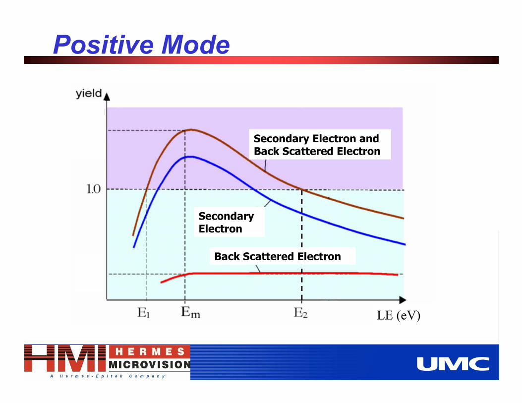
LE (eV)
Back Scattered Electron
Secondary
Electron
Secondary Electron and
Back Scattered Electron
Positive Mode

Poly
Poly
N+ P+
P N
Dark Bright Dark
eGate Oxide
Normal
Bright
Poly
N+
N
Bright
e P+
P
Bright
e
N+ P+
P N
Bright Bright Bright
eGate Oxide
Leakage
(BVC
defects)
Bright
Poly
N+
N
Bright
e P+
P
Bright
eee
e
This study
W-Plugs & VC in Positive Mode

Experiment 1
� 6 wafers
� 3 ion implantation conditions
� After WCMP
�One wafer from each condition send to
inspection
� Another one continue to M1 for WAT
� Inspected and measured test keys and
SRAM arrays

Leak
age C
urren
tBVC Defect C
ount
Split 1 Split 2 Split 3
BVC Defect
Correlation of WAT and eScan®

Correlation of WAT and eScan®Defect count
Split 1 Split 2 Split 3
Split 1 Split 2 Split 3

GLV Binning
� Strong leakage causes high GLV
� Auto binning GLV of all BVC defects
� High GLV BVC map matches with high
leakage current map very well.
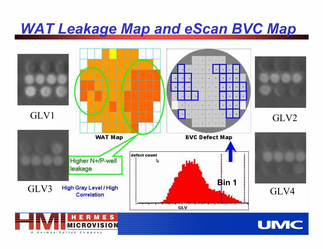
Bin 1
WAT Leakage Map and eScan BVC Map
GLV1 GLV2
GLV3 GLV4

Extrusion Length vs eScan GLV
Extrusion length GL vs NISI piping extruded length
L3 L4
L2L1
0
10
20
30
40
50
60
GLV4 GLV3 GLV2 GLV1

NiSi Diffusion
Leakage is caused by NiSi diffusion
SEM TEM

Experiment 2
� 13 wafers
� 3 ion implantation conditions
� eScan inspection on two test keys
�WAT after M1 CMP

BVC counts vs. WAT Leakage
Leakage current
BVC counts
R2 = 0.8079
R2 = 0.7464Test key 1 BVC Counts
Test key 2 BVC Counts
Test
key 1
Test
key 2Leakage current
WAT

Conclusion
� BVC defects of W-plugs that connect to NiSi on N+/P-well junction on both test key structures and SRAM array
� BVC defect counts correlate with WAT leakage current on both test key and SRAM
� FA delayer showed that N+/P-well leakage is caused by nickel silicide diffusion
� Extrusion length of the nickel silicide strongly correlates with GLV of the W-plug
� BVC counts strongly correlate to WAT leakage current

Development
� More EBI systems:� Leap Scan EBI : eScan®310, eScan®315 (Improve
resolution)
� Continue scan EBI : eScan®Lite (Improve throughput)
� Hotspot EBI: eP2
� More EBI applications� Monitoring hole non-open at contact AEI and WCMP.
� Qualifying the contact lithography process window.
� Negative ModeTM EBI for P+/N-well leakage detection.
� Monitoring NMOS and gate leakage right after NiSi formation.