layout synthesis - university of toronto t-space · 2020-04-07 · abstract routing architecture...
TRANSCRIPT

ROUTING ARCHITECTURE AND
LAYOUT SYNTHESIS
FOR MULTI-FPGA SYSTEMS
MOHAMMED A. S. KHALID
A Thesis submitted in conformity with the requirements for the Degree of Doctor of Philosophy in the
Department of Electrical and Cornputer Engineering, University of Toronto
O Copyright by Mohammed A. S. Khalid 1999

National Library 191 of Canada Bibliothèque nationale du Canada
Acquisitions and Acquisitions et Bibliogaphic Setvices sewices bibliographiques
395 Wellington Street 395, nie Wellington Ottawa ON K1A ON4 Ottawa ON Kt A ON4 Canada Canada
Your h& Votre relersnca
Our hle Nom reldrence
The author has granted a non- L'auteur a accordé une licence non exclusive licence dowing the exclusive permettant à la National Library of Canada to Bibliothèque nationale du Canada de reproduce, loan, distribute or sel1 reproduire, prêter, distribuer ou copies of this thesis in microfom, vendre des copies de cette thèse sous paper or electronic formats. la forme de microfiche/fiim, de
reproduction sur papier ou sur format électronique.
The author retains ownership of the L'auteur conserve la propriété du copyright in this thesis. Neither the droit d'auteur qui protège cette thèse. thesis nor substantid extracts fiom it Ni la thése ni des extraits substantiels rnay be printed or otherwise de celle-ci ne doivent être imprimés reproduced without the author's ou autrement reproduits sans son permission. autorisation.

Abstract
Routing Architecture and Layout Synthesis for Multi-FPGA Systems
Doctor of Philosophy, 1999 Mohammed A. S. Khalid
Department of Electrical and Computer Engineering University of Toronto
Multi-FPGA systems (MFSs) are used as custom computing machines, logic emula-
tors and rapid prototyping vehicles. A key aspect of these systems is their programmable
routing architecture, which is the manner in which wires, FPGAs and Field-Programmable
lnterconnect Devices (FPDs) are connected.
This dissertatior; provides new insight into the strengths and the weaknesses of two
popular existing routing architectures: the Partial Crossbar and the Mesh. New hybrid
architectures, that use a mixture of hardwired and programmable connections, are pro-
posed. The new architectures are the Hybrid Toms Partial-Crossbar (HTP), the Hybrid
Complete-Graph Partial-Crossbar (HCGP) and the Hardwired Clusters Partial Crossbar
(HWCP).
We evaluate and compare several MFS routing architectures by using a rigorous exper-
imental approach that employs real benchmark circuits. The circuits are mapped into the
architectures using a customized set of partitioning, placement and inter-chip routing
tools. The architectures are compared on the basis of cost (the total number of pins
required in the system) and speed (determined by the post-inter-chip routing critical path
del ay ).
The key parameters associated with the partial crossbar and the hybrid architectures
are explored. For the partial crossbar, the effect of varying the number of pins per subset
(P,), on the routability, speed, and cost is minor. For the hybrid architectures, a key param-
eter, the percentage of programmable connections (Pp), is explored and we experimentally
determined that Pp = 60% gives good routability across al1 the benchmark circuits.

We show that the Partial Crossbar is superior to the 8-way Mesh architecture. We
show that one of the newly proposed hybrid architectures, HCGP, is superior to the Partial
Crossbar. The HTP architecture is shown to be inferior to the HCGP and only marginally
better than the Partial Crossbar. The HWCP architecture is evaluated compared to the
HCGP architecture and gives encouraging routability and speed results.
Overall, the results show tliat for single board MFSs, the HCGP is the best among al1
the MFS routing architectures evaluated.
iii

Alhamdulillah (Praise be to God), this dissertation work has been finally completed.
First, 1 want to express my gratitude to the God almighty for enabling me to reach this
important milestone in rny life.
1 would like to express my heartfelt thanks to my supervisor Jonathan Rose for his
moral and financial support, guidance, and encouragement. Al1 the things that 1 learned
from him in the past five years, especially his cornmitment to excellence in research and
his remarkable presentation skills, will be very useful for the rest of my life. 1 would like
to thank the members of my thesis committee, Professors P. Chow, 2. Vranesic, T. Abdel-
rahman, G. Slemon and my external examiner Prof. S. Hauck. Their invaluable sugges-
tions were crucial in improving the clarity and readability of this dissertation.
1 would like to thank members of Jonathan's research group, Vaughn Betz, Mike Hut-
ton, Rob McCready, Sandy Marquardt, Yaska Sankar, Jordan Swartz, and Steve ilt ton for
their valuable technical discussions during our weekly group meetings. Al1 the colleagues
in LP392 deserve my thanks for making my stay so enjoyable. Mazen Saghir and Muham-
mad laseemuddin deserve my special thanks for their help on many occasions.
1 am indebted to my parents for their support and prayers throughout my life. 1 learned
from them the virtues of hard work, diligence, and forbearance which are crucial for any
signifiant achievement in life. 1 am grateful to my wife for patiently k i n g the rigors of
life for the past few years. This dissertation would not have been possible without her con-
stant love and support. 1 am thankful to my father-in-law and mother-in-law for their sup-
port and encouragement during this thesis work. My brothers, sisters, and cousins
provided much needed moral support and prayers. Last but not the least, 1 would like to
thank my three wonderful daughters Samira, Aisha, and Sarah for bringing so much joy
into my life.
Financial support for ihis project, provided by the ITRC and MICRONET, is gratefully
acknowledged.
Table of Contents
....................................... Chapter 1 Introduction .1
. . . . . . . . . . . . . . . . . . . . . . . . . . . . . . . . . . 1.1 MFS Routing Architecture 2
. . . . . . . . . . . . . . . . . . . . . . . . . . . . . . . . . . . . . . . . . . 1.2 Thesis Overview 4
....................... Chapter 2 Background and Previous Work 6
. . . . . . . . . . . . . . . . . . . . . . . . . . . 2.1 Multi-FPGA System Architectures 6
. . . . . . . . . . . . . . . . . . . . . . . . . . . . . . . . . . . . . . 2.1.1 Linear Arrays 8
. . . . . . . . . . . . . . . . . . . . . . . . . . . . . . . . . . 2.1.2 Mesh Architectures 9
2.1.3 Architectures that Employ only Programmable Interconnect
. . . . . . . . . . . . . . . . . . . . . . . . . . . . . . . . . . . . . . . . . . . Devices 11
. . . . . . . . . . . . . . . 2.1.4 Previous Research on MFS Architectures 14
. . . . . . . . . . . . . . . . . . . . . . . . . . . . . . . . . Mesh Architectures 14
. . . . . . . . . . . . . . . . . . . . . . . . . Partial Crossbar Architecture 16
. . . . . . . . . . . . . . . . . . . Studies on Other MFS Architectures 17
. . . . . . . . . . . . . . . . . . . . . . . . . . FPMCM Architecture Study 18
. . . . . . . . . . . . . . . . . . . . . . . . . 2.2 CAD Flow for Multi-FPGA Systems 20
. . . . . . . . . . . . . . . . . . . . . . . . . . . . . . . . 2.2.1 Alternate Approach - 2 2
. . . . . . . . . . . . . . . . . . . . . . . . . . . . . . . . . . . 2.3 Layout Synthesis Tools 22
. . . . . . . . . . . . . . . . . . . . . . . . . . . . . . . . . . . . . . . 2.3.1 Partitioning 23
Part: A Partitioning Tool Developed for the TM-1 MF$ . . . . 25 . . . . . . . . . . . . . . . . . . . . . . . . . . . . . . . . . . . . . . . . 2.3.2 Placement 26
. . . . . . . . . . . . . . . . A Force-Directed Placement Algorithm $26
. . . . . . . . . . . . . . . . . . . . . . . . . . . . . . . 2.3.3 Inter-FPGA Routing $ 2 9
. . . . . . . . . . . . . Routing Algorithms for the Partial Crossbar 30
. . . . . . . . . . . . . . Topology Independent Routing Algorithms 32

. . . . . . . . . . . . . . . . . . . . . . . . . . . . . . . . . . . . 2.3.4 Pin Assignment 33
. . . . . . . . . . . . . . . . . . . . . . . . . . . . . . . . . . . . . . . . . . . . . . . 2.4 Summary 33
......................... Chapter 3 MFS Routing Architectures -35
. . . . . . . . . . . . . . . . . . . . . . . . . . . . . . . . . . . . . . . 3.1 Basic Assumptions 35
. . . . . . . . . . . . . . . . . . . . . . . . 3.2 4-way and 8-way Mesh Architectures 37
. . . . . . . . . . . . . . . . . . . . . . . 3.3 Partial Crossbar Routing Architecture 38
. . . . . . . . . . . . . . . . . . . . . . . . . . . . . . . . . . . . . 3.4 Hybrid Architectures 39
. . . . . . . . . . . . . . . . . . . . . . . . 3.4.1 Hybrid Torus Partial-Crossbar 40
3.4.2 Hybrid Complete-Graph Partial-Crossbar . . . . . . . . . . . . . . . 42
3.4.3 Hardwired-Clusters Partial-Crossbar . . . . . . . . . . . . . . . . . . 44
. . . . . . . . . . . . . . . . . . . . . . . . . . . . . . . . . . . . . . . . . . . . . . . 3.5 Summary 45
Chapter 4 CAD Tools and Experimental Evaluation Framework . . 46
. . . . . . . . . . . . . . . . . . . . . . . . . . . . . . . . . . 4.1 Experimental Procedure 46
. . . . . . . . . . . . . . . . . . . . . . . . . . . . . . . . . . . . . . 4.1.1 Assumptions 48
. . . . . . . . . . . . . . . . . . . . . . . . . . . . . . . FPGA Pin Assignment 49
. . . . . . . . . . . . . . . . . . . . Intra-FPGA Placement and Routing 49
. . . . . . . . . . . . . . . . . . . . . . . . . . . . . . . . . . . . . . . 4.2 Evaluation Metrics 50
. . . . . . . . . . . . . . . . . . . . . . . . . . . . . . . . . . . . . . . . . . 4.2.1 Pin Cost 50
. . . . . . . . . . . . . . . . . . . . . . 4.2.2 Post-Routing Critical Path Delay 50
. . . . . . . . . . . . . . . . . . . . . . . . . . . . . . . . . . . . . . 4.3 Benchmark Circuits 50
4.4 CADTools . . . . . . . . . . . . . . . . . . . . . . . . . . . . . . . . . . . . . . . . . . . . . . 52
. . . . . . . . . . . . . . . . . . . . . . . . . . . . . . 4.4.1 Multi-way Partitioning 52
. . . . . . . . . . . . . . . . . . . . . . . . . . . . . . . . . . . . . . . 4.4.2 Placement - 5 5
. . . . . . . . . . . . . . . . . . . . . Placement for Mesh Architectures 55
. . . . . . . . . . . . . . . . . . Placement for the HWCP Architecture 57
. . . . . . . . . . . . . . . . . . . . . . . . . 4.4.3 MFS Static Timing Analyzer 58
Sample Results Obtained Using the MTA . . . . . . . . . . . . . . . 61
4.4.4 Inter-FPGA Routing Algorithms . . . . . . . . . . . . . . . . . . . . . . 62
A Topology-Independent Router . . . . . . . . . . . . . . . . . . . . . . . 62
Routing Algorithm for Mesh Architectures . . . . . . . . . . . . . . 64
Routing Algorithm for Partial Crossbar . . . . . . . . . . . . . . . . . 65

. . . . . . . . . . . . . Routing Algorithm for Hybrid Architectures 69
Timing-Driven Routing A1gonth.m for Hybrid Architectures 70
4.5 Summ ary . . . . . . . . . . . . . . . . . . . . . . . . . . . . . . . . . . . . . . . . . . . . . . . 73 .......... Chapter 5 Evaluation and Cornparison of Architectures 75
. . . . . . . . . . . . . . . . . . . . . . . . . . . 5.1 Analysis of Routing Architectures 75
. . . . . . . . . . . . . . . . . . . . . . . 5.1.1 Partial Crossbar: Analysis of Pt 76
. . . . . . . . . . . . . . . . . . . . 5.1.2 HCGP Architecture: Analysis of Pp 78
. . . . . . . . . . . . . . . . . . . . . 5.1.3 HTP Architecture: Analysis of Pp 80
. . . . . . . . . . . . . 5.1.4 HWCP Architecture: Analysis of Pp and Cs 80
. . . 5.2 Cornparison of 8-way Mesh and Partial Crossbar Architectures 83
. . . . . . . . . . . . . . . . . . . 5.3 Cornparison of HCGP and Partial Crossbar 86
. . . . . . . . . . . . . . . . . 5.4 Comparison of HTP and HCGP Architectures 89
. . . . . . . . . . . . . . . . . HTP Compared to the Partial Crossbar 91
. . . . . . . . . . . . . . . 5.5 Comparison of HWCP and HCGP Architectures 91
. . . . . . . . . . . . . . . . . . . . . . . . . . . . HWCP Compared to HTP 93
5.6 Summa ry . . . . . . . . . . . . . . . . . . . . . . . . . . . . . . . . . . . . . . . . . . . . . . . 94
....................... Chapter 6 Conclusions and Future Work 96
. . . . . . . . . . . . . . . . . . . . . . . . . . . . . . . . . . . . 6.1 Dissertation Summary 96
. . . . . . . . . . . . . . . . . . . . . . . . . . . . . . . . . . . 6.2 Principal Contributions 97
. . . . . . . . . . . . . . . . . . . . . . . . . . . . . . . . . . . . . . . . . . . . 6.3 Future Work 98
. . . . . . . . . . . . . . . . . . . . . . . . . . . . . . . . 6.3.1, CAD Tools for MFSs 98
. . . . . . . . . . . . . 6.3.2 Future MFS Routing Architecture Research 99
Appendiv A The Effects of Fixed II0 Pin Positioning on the Routabü-
............................ ity and Speed of FPGAs 101
. . . . . . . . . . . . . . . . . . . . . . . . . . . . . . . . . . . . . . . . . . . A.l Introduction 101
. . . . . . . . . . . . A.2 Benchmark Circuits and Experimental Procedure 102
. . . . . . . . . . . . . . . . . . . . . . . . A.3 Experimental Results and Analysis 105
A.3.1 Results for the Xilinx XC4000 FPGAs . . . . . . . . . . . . . . . . . 106
A.3.2 Results for the AItera FLEX 8000 FPGAs . . . . . . . . . . . . . . 112
. . . . . . . . . . . . . . . . . . . . . . . . . . . . . . . . . . . . . . . . . . . A.4 Conclusions 117
v i i

Appendix B Experimental Results Showing Actual Pin Cost and Delay
Values ........................................... 119 References .................................................. 125
viii

List of Tables
Table 4-1:
Table 4-2:
Table 4-3:
Table 4-4:
Table 4-5:
Table 4-6:
Table 5-1:
Table 5-2:
Table 5-3:
Table 5-4:
Table 5-5:
Table 5-6:
Table 5-7:
Table A-1:
Table A-2:
Table A-3:
Table A-4:
Table A-5:
Table A-6:
Table B-1:
Table B-2:
Table B-3:
Table B-4:
Table B-5:
Benchmark Circuits . . . . . . . . . . . . . . . . . . . . . . . . . . . . . . . . . . . . . . . . . 51
. . . . . . . . . . Placement Results for Different Values of iteration-limit 56
. . . . . . . . . . . . . The Delay Values Used in the Timing Analyzer Mode1 59
Critical Path Delays at Different Levels of Circuit Implernentation . . 61
. . . . . . . . . . . . . . . . . . . . . . Cornparison of FPSROUTE and MROUTE 65
. . . . . . . . . . . . . . . . . . . . . Comparison of HROUTE and HROUTETD 72
. . . The Effect of Pt on the Delay of the Partial Crossbar Architecture 76
. . . . . . . . . . . . . . The Effect of on the Delay of the HCGP Architecture 79
The Minimum Pp Value Required for Routing Completion in HWCP . 82
Comparison of the 8-way Mesh and Partial Crossbar Architectures . . 84
Comparison of the HCGP and Partial Crossbar Architectures . . . . . . . 87
Comparison of the HTP and HCGP Architectures . . . . . . . . . . . . . . . . . 89
Cornparison of the HWCP and the HCGP Architectures . . . . . . . . . . . . 92
Critical Path Delay Under Different Pin Constraints for the Xilinx FP-
G h . . . . . . . . . . . . . . . . . . . . . . . . . . . . . . . . . . . . . . . . . . . . . . . . . . . . . 105
Routing Resource Utilization in the Xilinx FPGAs . . . . . . . . . . . . . . . 108
Routing Resource Utilization Statistics for the Xilinx FPGAs . . . . . . 110
Critical Path Delay Under Different Pin Constraints for the Altera FP-
GAs . . . . . . . . . . . . . . . . . . . . . . . . . . . . . . . . . . . . . . . . . . . . . . . . . . . . . 112
Routing Resource Utilization for the Altera F P W . . . . . . . . . . . . . . 114
Routing Resource Utilization Statistics for the Altera FPGAs . . . . . . 116
Cntical Path Delays at Different Levels of Circuit Implementation . 119
Cornparison of HROUTE and HROUTETD . . . . . . . . . . . . . . . . . . . . 120
The EEect of Pp on the Delay of the Partial Crossbar Architecture . 121
Comparison of the HCGP and Partial Crossbar Architectures . . . . . 122
Cornparison of the HTP and HCGP Architectures . . . . . . . . . . . . . . . 123

Table B-6: Cornparison of the HWCP and HCGP Architectures . . . . . . . . . . . . . 124
List of Figures
. . . . . . . . . . . . . . . . . . . . . . . . . . . . . . . . Figure 1-1: A Generic Multi-FPGA System 2
Figure 1-2: MFS Routing Architectures Using (a) Hardwired Connections (b) Pro-
. . . . . . . . . . . . . grammable Connections (c) Both Types of Connections 3
. . . . . . . . . . . . . . . . . . . . . . . . . . . . . . . . Figure 2-1: The AnyBoard System [Van921 8
Figure 2-2: Mesh Architectures: (a) 4-way Mesh (b) Torus ( c ) 8-way Mesh . . . . . . 9
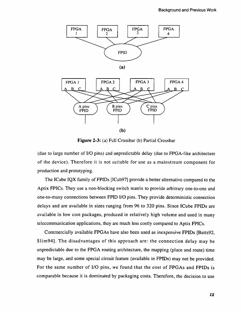
. . . . . . . . . . . . . . . . . . . . . . . . . . Figure 2-3: (a) Full Crossbar (b) Partial Crossbar 12
. . . . . . . . . . . . . . . . . . . . . . . Fi y r e 2-4: The TM-2 Routing Architecture [Lewi98] 13
. . . . . . . . . . . . . . . . . . . . . . . . . . . . . . . Figure 2-5: Connections in l-Hop Topology 15
Figure 2-6: Connections in a 4-way Mesh: (a) Without Superpins (b) With Super-
pins . . . . . . . . . . . . . . . . . . . . . . . . . . . . . . . . . . . . . . . . . . . . . . . . . . . . . . 15
. . . . . . . . . Figure 2-7: Example of Tri-partite Graph Topology Using Six FPGAs 18
. . . . . . . . . . . . . . . . Figure 2-8: Programmable Interconnection Frame Structure 19
. . . . . . . . . . . . . . . . . . . . . . . . . . . . . . . . . . . Figure 2-9: The Design Flow for MFSs 20
Figure 2-10: A Force-directed Placement Algorithm using Ripple Moves . . . . . . . 28
. . . . . . . . . . . . . . . . . . . . . . . . Figure 2-11: Inter-FPGA Routing in a 4-way Mesh 29
Figure 3-1: Mesh Architectures: (a) 4-way Mesh (b) û-way Mesh (c) 4-way Torus (d)
8-wayTorus . . . . . . . . . . . . . . . . . . . . . . . . . . . . . . . . . . . . . . . . . . . . . . . 36
Figure 3-2: Extreme Cases of the Partial Crossbar: (a) Pt = 192. (b) Pt = 1 . . . . . 39
Figure 3-3: The HTP Architecture . . . . . . . . . . . . . . . . . . . . . . . . . . . . . . . . . . . . . . 40
Figure 3-4: The HCGP Architecture . . . . . . . . . . . . . . . . . . . . . . . . . . . . . . . . . . . . . 42
Figure 3-5: Multi-terminal Net Routing: (a) Without an FPID (b) With an FPID . 43 Figure 3-6: The HWCP Architecture . . . . . . . . . . . . . . . . . . . . . . . . . . . . . . . . . . . . 44
Figure 3-7: Different Cluster Sizes for HWCP (a) Cs = 3 (b) Cs = 4 . . . . . . . . . . . . 45 Figure 4-1: Experimental Evaluation Procedure for MFSs . . . . . . . . . . . . . . . . . . . 47
Figure 4-2: Pseudo-code for RBT . . . . . . . . . . . . . . . . . . . . . . . . . . . . . . . . . . . . . . . 53
Figure 4-3: The Partitioning Tree for the Circuit spsdes Generated by RBT . . . . 54

Figure 4-4: Semi-perimeter of the Net Bounding Box . . . . . . . . . . . . . . . . . . . . . . . 55
Figure 4-5: Partitioning and Placement of the s35932 circuit on the HWCP Archi-
tecture: (a) Actual (b) Ideal . . . . . . . . . . . . . . . . . . . . . . . . . . . . . . . . . . . 58
Figure 4-6: (a) 4-way Toms architecture (b) Its Routing Graph . . . . . . . . . . . . . . . 63
Figure 4-7: Pseudo-code for the Routing Algorithm used in PCROUTE . . . . . . . . 66
Figure 4-8: Multi-hop Routing in Partial Crossbar . . . . . . . . . . . . . . . . . . . . . . . . . 68
Figure 4-9: Pseudo-code for the Routing Algorithm used in HROUTE . . . . . . . . . 70
Figure 4-10: Timing-driven Routing Algonthm for the Hybrid Architectures . . . . 71
Figure 5-1: The Effect of Pp on the Routability of the HCGP Architecture . . . . . . 78
Figure 5-2: The Effect of Pp on the Routability of the HTP Architecture . . . . . . . 81
Figure 5-3: The Effect of Pp on Routability of HWCP Architecture (~38417 circuit)
82
Figure 5-4: Routing in the Mesh (a) Non-local Net (b) Multi-terminal Net . . . . . 86
Figure 5-5: Hardwired connections in the HTP architecture . . . . . . . . . . . . . . . . . 91
Figure A-1: Experimental Procedure for the Xilinx FPGAs . . . . . . . . . . . . . . . . . 103
Figure A-2: Experimental Procedure for the Altera FPGAs . . . . . . . . . . . . . . . . 104

Glossary
Acronyms
MFS Multi-FPGA Systern
FPID Field Programmable Interconnect Device
MCM Multi-Chip Module
FPMCM Field Programmable Multi-Chip Module
HTP Hybrid Torus Partial Crossbar
HCGP Hybnd Complete Graph Partial Crossbar
HWCP Hardwired Clusters Partial Crossbar
Architecture Parameters
p, The number of pins per subset, an important parameter in the partial crossbar architecture
P~ The percentage of programmable connections, an important parameter in the hybrid architectures
CS The cluster size, an important parameter in the HWCP archi- tecture
xiii
Introduction
Field-Programmable Gate Arrays (FPGAs) are widely used for implementing digital
circuits because they offer moderately high levels of integration and rapid tumaround time
[Brow92, Trim941. Multi-FPGA Systems (MFSs), which are collections of FPGAs joined
by programmable connections [HaucgSa], are used when the logic capacity of a single
FPGA is insufficient, and when a quickly reprogrammed system is desired. MFSs are used
in logic emulation [Babb97, Apti98, Quic981, rapid prototyping [Van92, Ga1194, AIte94,
Lewi981 and reconfigurable custom computing machines [Arno92, Cass93, Dray95,
Vui1961. In some of these applications, MFSs have produced the highest performance
to-date, surpassing even the most powerful supercomputers [Gokh9 l][Vuil96]. The
subject of this dissertation is the exploration of the routing architectures for MFSs.
Logic emulation is the most important application of MFSs. Logic emulators map a
structural (netiist) representation of an ASIC or a microprocessor design into an MFS. The
design is operated at speeds ranging from hundreds of KHz to a few MHz. This is several
orders of magnitude faster than software design simulation speeds, which are restricted to
nt most few tens of Hertz. This allows functional verification of the design in its target
operating environment that includes other hardware and software modules [Butt95]. Many
functional errors, that are impossible to detect by simulation due to prohibitively long
execution times, can be discovered and fixed before IC fabrication. Thus very costly
Introduction
Hardw ifcd connectrons FPGA
FPGA FPGA FPGA
I
Interconncc tian FPGA
FPGA . FPGA FPGA
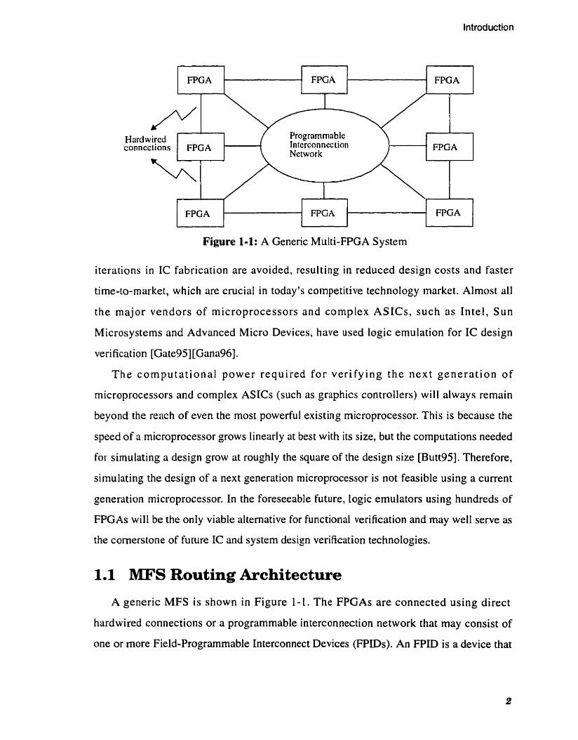
Figure 1-1: A Generic Multi-FPGA System
iterations in IC fabrication are avoided, resulting in reduced design costs and faster
time-to-market, which are crucial in today's competitive technology market. Alrnost al1
the major vendors of microprocessors and complex ASICs, such as Intel. Sun
Microsystems and Advanced Micro Devices, have used logic emulation for IC design
verification [Gate951 [Gana96].
The computational power required for verifying the next generation of
microprocessors and complex ASICs (such as graphics controllers) will always remain
beyond the reach of even the most powerful existing microprocessor. This is because the
speed of a microprocessor grows linearly at best with its size, but the computations needed
for simulating a design grow at roughly the square of the design size [Butt95]. Therefore,
simulating the design of a next generation microprocessor is not feasible using a current
generation microprocessor. In the foreseeable future, logic emulators using hundreds of
FPGAs will be the only viable alternative for functional verification and may well serve as
the cornerstone of future IC and system design verification technologies.
MFS Routing Architecture
A generic MFS is shown in Figure 1-1. The FPGAs are connected using direct
hardwired connections or a programmable interconnection network that may consist of
one or more Field-Programmable Interconnect Devices (FPIDs). An FPID is a device that

Introduction
can be programmed to provide arbitrary connections between its VO pins. One-to-one and
FPGA
one-to-many connections between its pins can be realized by the FPID.
The routing architecture of an MFS is the way in which the FPGAs, fixed wires and
I - FPGA FPGA
(a)
r
FPGA FPGA
(c )
FPG A FPGA FPG A
(b) Figure 1-2: MFS Routing Architectures Using (a) Hardwired Connections (b)
Programmable Connections (c) Both Types of Connections
programmable interconnect chips are connected. The routing architecture has a strong
FPGA -
effect on the speed, cost and routability of the system because an inefficient routing
FPGA
architecture may require excessive logic and routing resources when implementing
circuits and cause large routing delays.
There are many such routing architectures. For example, consider those shown in
Figure 1-2. We refer to wires directly connecting two FPGAs as hardwired connections.
Wires that connect an FPGA to an FPID are called programmable connections. Figure
1 -2(a) shows an FPGA-only architecture that uses only hardwired connections. Figure
1 4 b ) shows an architecture that uses only programmable connections (no hardwired
connections). Figure 1-2(c) shows an architecture that uses both hardwired and

Introduction
programmable connections. Given the multitude of choices in the architectural exploration
space, it is difficult even to decide on a starting point in MFS architecture research.
The goals of this research are to evaluate and compare difTerent routing architectures
for MFSs. We address the following questions:
Which routing architecture topology is the best in terms of cost, speed, and routabil-
i ty ?
What is the effect of using hardwired inter-FPGA connections? If they are useful,
what are the percentages of programmable and hardwired connections that give the
best results for different architectures?
We use an experimental approach to evaluate and compare different architectures. A
total of fifteen large benchmark circuits are used in our experimental work. The
benchmark circuits are mapped to different architectures using a customized set of
architecture-appropriate mapping tools. The architectures are evaluated and compared on
the basis of cost and speed metrics. The speed comparisons are based on post inter-chip
routing critical path delay of real benchmark circuits, which, to Our knowledge, is the first
time such detailed timing information has been used in the study of board-level MFS
architectures.
We started this research by evaluating and cornparing two commonly used routing
architectures namely. the mesh and the partial crossbar [Butt92]. The insight and the
experience gained in this task enabled us to propose a better routing architecture, called
the Hybrid Complete-Graph Partial-Crossbar (HCGP), that gives superior cost and speed
[Kha198].
1.2 Thesis Overview
This dissertation is organized as follows:
In Chapter 2 we describe the previous work on MFS routing architectures and
mapping CAD tools.
In Chapter 3, we present detailed descriptions of al1 the routing architectures explored
in this research. We also cover the issues and assumptions that arise when mapping real

Introduction
circuits to the various architectures. The architectures explored are mesh, partial crossbar,
and some newly proposed hybrid architectures. The mesh uses only hardwired
connections, the partial crossbar uses only programmable connections. The hybrid
architectures use a mixture of hardwired and programmable connections.
Chapter 4 describes the framework used for experimental evaluation of MFS routing
architectures. The experimental procedure used for mapping circuits to architectures is
described. The metrics used for evaluating and cornparing architectures are explained and
the detnils of the benchmark circuits used are presented. The customized set of mapping
tools used in this work are described in detail. These are architecture-speci fic (board-level)
inter-chip routers, a board-level placement tool, and a static timing analysis tool for MFS
architectures.
Chapter 5 presents the key results frorn this research. For several architectures, we
explore key parameters associated with each architecture. We compare different
architectures and show that the partial crossbar is one of the best existing architectures.
The newl y proposed hybrid cornplete-graph partial-cross bar architecture is shown to be
superior to the partial crossbar. The proposed hybrid architectures and their detailed
evaluation is the main contribution of this thesis.
We conclude and describe topics for future work in Chapter 6.

Background and Previous Work
Since the early 1990s, many MFSs and the associated CAD tools have been proposed
and built for logic emulation, rapid prototyping and a wide variety of applications in
custom computing. These systems and their CAD tools are the focus of this chapter. An
overview of existing MFSs and their routing architectures is presented in Section 2.1. The
design flow used in mapping large circuits to MFSs is described in Section 2.2. In Section
2.3, the various mapping tools and algorithms for each of the steps in the design flow are
reviewed.
2.1 Multi-FPGA System Architectures
The MFSs that have been previously developed range from small systems that fit on a
single printed circuit board [Ga11941 to huge systerns that use hundreds of FPGAs laid out
on tens of Printed Circuit Boards (PCBs), which in turn are mounted in many card cages
[Qu ic981.
An overwhelming majority of MFSs have been implemented on PCBs. However, a
few MFSs based on Multi-Chip Modules (MCMs) have been proposed and built
[Dobb92] [Dam941 [Amer951 [Lang51 [Terr95]. In these Field-Programmable Multi-Chip
Modules (FPMCMs), several FPGA dies are mounted on a single substrate,
interconnection resources are provided, and al1 the logic and routing resources are

Background and Previous Work
packaged as a single unit. The advantages of MCMs compared to PCBs are reduced size,
power consumption and superior speed performance. This approach is still in its infancy
and a number of issues like FPMCM cost, architectures, yield, interconnect density, and
thermal dissipation nced to be resolved before FPMCMs become commercially viable. In
this chapter we will concentrate on MFSs implemented using PCBs.
Many MFSs were built for specific applications, such as the Marc-1, which was
designed to perform circuit simulation [Lewi93] and the RM-nc which was used for
neural-network simulation [Erdo92]. Their topologies are optimized for specific
applications and it is hard to categorize such unique topologies. Since the focus of this
research is on general purpose reprogrammable MFSs, we will not review such systems.
In addition to FPGAs, almost al1 MFSs have memory chips and other devices such as
small dedicated FPGAs or microcontrollers for 'housekeeping' tasks such as controlling
communication with the host computer, system configuration and status monitoring
[Babb97]. For example each board in the TM-2 system [Lewi98] consists of two Altera
lOK50 FPGAs, four 1-Cube FPIDs, 8 Mbytes of memory, and one FPGA each for
programmable dock generation and housekeeping respectively. The current trend in MFSs
(especially in logic emulators) is to provide RISC processors and sockets for DSPs and
Intellectual Property (IP) cores in addition to FPGAs [Baue98, Cour971 to widen their
range of applications. Even i n such systems, the routing architecture used for
interconnec ting the FPGAs remains important.
The routing architecture of an MFS is defined by the topology used to connect the
FPGAs. Another distinguishing feaiure is whether programmable interconnect chips, also
called FPIDs or crossbars in the literature, are used for connecting the FPGAs. If no FPIDs
are used we refer to i t as an FPGA-only architecture. The existing routing architectures
can be categorized roughly in the following three ways: linear arrays, meshes, and
architectures that use programmable interconnect chips. The first two categories are
examples of FPGA-only architectures.

Background and Previous Work
Global Bus
Figure 2-1: The AnyBoard System [Van921
C
2.1.1 Linear Arrays
In this architecture the FPGAs are arranged in the form of a linear array, which is
suitable for one-dimensional systolic processing applications. This architecture has
extremely limited routing flexibility and many designs may run out of routing resources
and hence cannot be implemented. While the architecture may perform well i n certain
niche applications, it's utility as a general purpose MFS is very limited. Two well known
examples of this architecture are Splash [Gokh91] and AnyBoard [Van92].
The AnyBoard system uses fwe XiIinx 3090 FPGAs and three 128K x 8 RAMs as
shown in Figure 2- 1. Note that FPGAs at the opposite ends of the array are connected to
form a ring topology and al1 the FPGAs are connected to a global bus. An extension of the
global bus with dedicated VO lines from each FPGA serves as the system interface. This
can be used for routing UO signals of the circuits. The control FPGA is used to implement
circuitry for managing the PC bus interface, FPGA configuration management and
hardware debugging support. The purpose of using the control FPGA is to leave al1 the
logic in other FPGAs for implementing the required design functionality. The AnyBoard
system was one of the earliest MFSs built for rapid prototyping of small designs. It was an
inexpensive system that demonstrated the potential of MFSs as an attractive and low-cost
medium for rapid prototyping of many hardware designs.
XC3090 FPGA
A A A
-
CONTROL Data
XC3090 FPGA
Data v v
v v
-
Address b
XC3090 FPG A
b - q 128K X8
RAM 128K X 8
RAM 1 28K X 8
RAM
XC3090 FPGA
- 4 +
PC Interface
- XC3090 FPG A

Background and Previous Work
I I 1
t 1 7 1 1
FPGAb r FPGA
I 1 '
-
FPGA
Figure 2-2: Mesh Architectures: (a) Cway Mesh (b) Toms (c) 8-way Mesh
FPGA
I 1 - I
FPGA
L
The Splash system employed a linear array of 32 Xilinx 3090 FPGAs augrnented with
memory and FIFO devices. It was used to implement a systolic algorithm for genetic
string rnatching and shown to be 300 times faster than the Cray-2 supercornputer. The
Splash 2 system [Arno921 (the successor of Splash) improved the Splash architecture by
using a large crossbar chip for routing non-local connections between FPGAs in the linear
array. Hence, Splash-2 is a hybrid architecture that does not fit into any specitic category
of routing architectures given in this chapter.
I I - I
FPGA
FPGA
2.1.2 Mesh Architectures
In the simplest mesh architecture, the FPGAs are laid out in the form of a
two-dimensional array with each FPGA connected to its horizontal and vertical adjacent
neighbours as shown in Figure 2-2(a). Variations of this basic topology may be used to
improve the routability of the architecture such as the toms and 8-way mesh as shown in
Figure 2-2(b) and Figure 2-2(c). The advantages of mesh are simplicity of local
, u FE'GA - u
-
I 1 J
- #
FPGA
I I I
FPGA. -
FPGA FPGA
FPGA FPGA . a -

Background and Previous Work
interconnections and easy scalability. However, using FPGAs for interconnections reduces
the number of pins for logic inside each FPGA and leads to poor logic utilization. The
connection delays between widely separated FPGAs (especially in bigger arrays) are large
whereas those between adjacent FPGAs are small. This results in poor speed performance
and timing problems such as setup and hold time violations due to widely variable
interconnection delays. Notable examples in this category are the Quickturn RPM
[Waltg 1 1 , DEC PeRLe-1 [Vui196], and the MIT Virtual Wires project [Babb97].
The Quickturn RPM was the first commercial logic emulation system. Due to the
routability and speed problems of the mesh architecture that arise when implementing
general logic circuits, Quickturn switched to a superior architecture (partial crossbar) in
their next generation logic emulation systems [Butt92].
Some of the disadvantages of the mesh architecture were overconie in the MIT Virt~ial
Wires project by using a software technique called virtual wires [Babb97]. The FPGA pins
are used for both logic and routing in the mesh, and hence there are not enough pins
available for logic in each FPGA. Virtual wires overcomes this pin limitation problem by
intelligently multiplexing many logical wires (connections between partitioned
sub-circuits) on eacli physical wire in the mesh and pipelining these connections at the
maximum clocking frequency of the FPGA. In this way the number of pins available in
each FPGA can be effectively increased leading to higher logic utilization per FPGA.
Demonstration hardware boards were built, each using 16 Xilinx 4005 FPGAs
arranged as a Cway mesh. Each FPGA has 22 VO lines dedicated to a 64K X 4 SRAM
chip. A SPARC microprocessor was successfully emulated in a system environment and
booted the Alewife operating system at 180 KHz [Babb97]. This technology has been
cornmercialized and emulators using this architecture are being produced by IKOS
Systems [Ikos98].
The advantage of using the virtual wires scheme on a mesh is low-cost logic ernulation
because inexpensive low pin count FPGAs can be used and the mesh architecture is
relatively easy to manufacture. The disadvantages are the speed penalty and increased
mapping software complexity due to pin rnultiplexing. Also, it may be very difficult to

Background and Previous Work
map portions of asynchronous logic that may be present in the circuit being emulated
because asynchronous signals cannot be assigned to a specific time slice (phase) in the
emulation dock period. Finally, i t should be noted that virtual wires is a software
technique, and using it on other architectures (instead of a mesh) rnay give better speed
resul ts.
The rnesh architecture also does extremely well when implementing algorithms that
match its topology. This has been convincingly demonstrated by the DEC PeRLe- 1 system
which uses a 4-way mesh of 16 Xilinx 3090 FPGAs augmented by 7 control FPGAs, 4
MB of static RAM, four 64-bit global buses and FIFO devices. For many diverse
applications, such as cryptography, image analysis, high energy physics, and
therrnodynmics, this system gave superior performance and cost compared to every other
contemporary technology, including sopercomputers, massively parallel machines, and
conventional custom hardware [Vui196].
2.1.3 Architectures that Employ only Programmable Interconnect Devices
In these architectures al1 the inter-FPGA connectioiis are realized using FPIDs. An
ideal architecture would be a fu l l crossbar that uses a single FPID for connecting al1
FPGAs. as shown in Figure 2-3(a). Unfortunately, the complexity of a full crossbar grows
as a square of its pin count and hence i t is restricted to systems that contain at most a few
FPGAs. Before we discuss the exisiing MFS architectures that use FPIDs, we briefly
review existing FPID device architectures, their cost and commercial viability issues. We
also discuss the pros and cons of using commercially available FPGAs as FPIDs.
The first FPID introduced in the market was the Aptix FPIC (a synonym for FPID)
device [Guo92]. Each FPIC has 1024 pins arranged in a 32 x 32 Y0 pin matrix. Each pin
connects to two VO tracks that orthogonally cross routing channels. Each routing channel
consists OF sets of parallel tracks that are segmented into various sizes to accommodate
signal paths with different lengths. Bidirectional pass transistors controlled by SRAM
cells connect y0 tracks to routing tracks and routing tracks to other routing tracks. By
selectively programming the SRAM cells, the user can connect any device pin to any
number of other pins. The Aptix FPID has a number of disadvantages such as high cost
Background and Previous Work
FPGA FPGA FPGA FPGA I 2 3 4
1 FPGA 1 ( 1 FPGA2 ( ( FPGA 3 I
(b)
Figure 2-3: (a) Full Crossbar (b) Partial Crossbar
(due to large number of I/O pins) and unpredictable deley (due to FPGA-like architecture
of the device). Therefore i t is not suitable for use as a mainstream component for
production and prototyping.
The ICube IQX family of FPlDs [ICub97] provide a better alternative compared to the
Aptix FPICs. They use a non-blocking switch matrix to provide arbitrary one-to-one and
one-to-many connections between FPID I/O pins. They provide deterministic connection
delays and are available in sizes ranging from 96 to 320 pins. Since ICube FPIDs are
available in low cost packages, produced in relatively high volume and used in many
telecommunication applications, they are much less costly compared to Aptix FPICs.
Commercially available FPGAs have also been used as inexpensive FPIDs [Butts92,
Slim941. The disadvantages of this approach are: the connection delay may be
unpredictable due to the FPGA routing architecture, the mapping (place and route) time
may be large, and some special circuit feature (available in FPIDs) may not be provided.
For the same number of I/O pins, we found that the cost of FPGAs and FPIDs is
comparable because it is dorninated by packaging costs. Therefore, the decision to use

Background and Previous Work
Figure 2-4: The TM-2 Routing Architecture [Lewi98]
FPIDs or FPGAs (as FPIDs) should be based on other features such as delay
characteristics, device mapping and configuration tirne, etc.
The partial crossbar architecture [Butt92, Varg931 overcomes the limitations of the full
crossbar by using a set of small crossbars. A partial crossbar using four FPGAs and three
FPIDs is illustrated in Figure 2-3(b). The pins in each FPGA are divided into N subsets,
where N is the number of FPIDs in the architecture. A11 the pins belonging to the same
subset in different FPGAs are connected to a single FPID. The number of pins per subset
is a key architectural parameter that determines the nurnber of FPIDs needed and the pin
count of each FPID (this will be discussed in detail in Chapter 3). The delay for any
inter-FPGA connection is uniform and is equal to the delay through one FPID. The size of
the FPIDs (determined by pin count) increases only linearly as a fraction of the number of
FPGAs.
Partial crossbars can be used in a hierarchical manner to provide interconnections in
large systems. A set of crossbars at the board level can interconnect multiple FPGAs, at
the next level, another set of crossbars can interconnect multiple boards, and finally
another set of crossbars can interconnect multiple card cages. The delay for going from
one level to another increases, but it is still predictable and uniform. This architecture is
used in the System Realizer, a logic emulation system produced by Quickturn Design
Systems with an estimated logic capacity of three million gates [Quic98].
One difficulty with the (uniform) partial crossbar is that the wiring is very non-local,
which causes a major manufacturing problem when the FPGAs are spread out across

Background and Previous Work
many boards. The number of connections required between the boards requires expensive
high pin count connectors and back planes that can handle high wiring densities. These
problems are alleviated in the Transmogrifier-2 (TM-2 for short) architecture [Lewi97]
[Lewi98] developed at the University of Toronto. The TM-2 takes advantage of the natural
hierarchy and resulting locality of wiring within circuits. It uses a modified partial
crossbar architecture thnt maintains the constant routing delay of a partial crossbar but
utilizes more local connections to substantially reduce the back plane wiring density. A
hierarchical interconnect structure is used that requires N levels of routing for ZN FPGAs.
The number of wires in routing level k is more than the number of wires in routing level
k + l . A TM-2 system using four FPGAs (two routing levels) and four FPIDs is illustrated
in Figure 2-4. The thick fines indicate level 1 routing and the thin lines indicate level 2
routing. The largest version of the TM-2, called the TM-ZA, will comprise 16 boards that
each contain two Altera 1OKlOO FPGAs and up to 8 Mbytes of memory, providing an
estimated logic capacity of two million gates.
Other examples of MFSs in this category are the Aptix AXB-AP4 [Apti93] and the
Transmogrifier-1 [Ga1194]. These architectures use very high pin count Aptix
Field-Programmable Interconnect Components (FPIC, a synonym for FPID) [Guo92].
These systems are expensive due to high cost of the 1024-pin FPIC used and are difticult
to manufacture, especially for larger MFS sizes.
2.1.4 Previous Research on MFS Architectures
There have been a number of research efforts relating to MFS architectures that
predate the present work. We summarize them in this section.
Mesh Architectures
Hauck et al proposed several constructs to improve the basic 4-way mesh [Hauc94,
Hnuc951. In the 8-way mesh, each FPGA connects to its diagonal adjacent neighbours in
addition to horizontal and vertical adjacent neighbours. The 1-hop topology is similar to
the 4-way mesh but with additional connections io 'next-to-adjacent' FPGAs as well, both
horizontally and vertically, as illustrated in Figure 2-5. These topologies result in a

Background and Previous Work
Figure 2-5: Connections in 1 -Hop Topology
reduction of routing cost in the mesh (measured in terms of intermediate FPGA pins
required for connecting non-adjacent FPGAs).
Superpins and permutations are techniques that minirnize interna1 FPGA routing
resource usage when routing inter-FPGA nets. For example, in a 4-way mesh each FPGA
communicates with its four nearest neiglibours; logically north, south, east, and West, as
illustrated in Figure 2-6(a). If a signal passing through an FPGA enters from the north side
and leaves from the south side, it has to traverse the entire FPGA chip. This increases
Superpin
Figure 2-6: Connections in a Cway Mesh: (a) Without Superpins (b) With Superpins
I I
-
.
I l I I *
N N N N N N N N W W E W E
FPGA E W E W E W E W
S S S S S S S S S
N -
.
E -
-E - -
. .
E - -
N S E W N S E W N S S
E N FPGA w
N S S E E W W .
N S E W N S E W

Background and Previous Work
intra-FPGA routing cost and delay. Using the superpins technique, the 110 pins in an
FPGA are connected to adjacent FPGAs using an alternating pattern illustrated in Figure
2-6(b). With this arrangement, a signal passing through the chip need only traverse the
Iength of at most a few pins inside the FPGA, rather than the whole FPGA chip. A
'permutation' of superpins is a way of connecting superpins in adjacent FPGAs. A better
permutation (that reduces inter-FPGA routing costs) connects adjacent superpins in one
FPGA to non-adjacent superpins in the other FPGA.
To evaluate these topologies and techniques, a synthetic netlist was generated for a 5 x
5 array of FPGAs. The netlist was obtained by using a random distribution of sources and
sinks across a 5 x 5 array of FPGAs. The FPGAs were represented as grids with 36 pins on
a side. The inter-FPGA routing delay was assumed to be 30 times greater than the unit
intra-FPGA routing delay. Using a well known routing tool called the PathFinder
[McMu95], the synthetic netlist was routed on different topologies. The average and
maximum source-sink delays were calculated for each topology. The study showed that in
terrns of routing delay, the 8-way topology is 21% better than the Cway topology and the
1-hop is 36% better. Superpins improve the 1-hop topology by 3 1 % , with permutations
giving a further 5% improvement.
The limitations of this study are: First, i t uses synthetic netlists instead of
post-partitioning and placement netlists for real circuits. The effectiveness of the improved
topologies in routing real circuits is not proven; Second, no multi-terminal nets (one
source, multiple sinks) are used in the netlists. In mesh topologies, routing multi-terminal
nets is difficult [Tess97] and consumes excessive inter-FPGA routing resources (pins in
intermediate FPGAs). It is not clear if these reductions in delay offered by the improved
topologies for synthetic netlists will apply for real circuits. The Superpins and
permutations techniques, however, are valuable and could potentially provide significant
reductions in intra-FPGA routing resource utilization and delay for real circuits.
Partial Crossbar Architecture
Recall from Section 2.1.3 that the number of pins per subset is a key parameter of the
partial crossbar that determines the number of FPIDs required and the size (pin count) of

Background and Previous Work
each FPID. Its effect on the routability of the partial crossbnr is investigated in [Butt92].
Different types of synthetic netlists are mapped to different configurations of the partial
crossbar and the percentage of nets routed for each case are reported. It is shown that low
pin count FPIDs, which are cheaper, are almost as effective as high pin count FPIDs for
the partial crossbar.
In [Chan931 architectural trade-offs in the design of folded Clos networks (partial
crossbar) are discussed qualitatively. A Clos network [Clos531 is a three-stage
interconnection network that can be used to connect FPGAs in an MFS. Each inter-FPGA
connection, however, will incur a delay of three stages. In a folded Clos network, the
switches in the two outer stages are implemented inside the FPGAs and the switches in the
middle stage are implernented using FPIDs [Chan93]. The routing resources needed for
implementing outer stage switches within FPGAs affects their routability and logic
utilization. There is a trade-off here; reducing the size of the switches in the outer stages
improves the routability and logic utilization of individual FPGAs but requires larger
FPIDs in the rniddle stage and adversely affects the routability of the folded Clos network,
and vice versa.
An optimal algorithm for routing two-terminal nets in the folded clos network is
presented. It is dernonstrated that the routing problem for multi-terminal nets has no
optimal solution.
Studies on Other MF's Architectures
Although the studies discussed above provide some insight into the mesh and partial
crossbar architectures, empirical studies that evaluate the implementation of real circuits
on different architectures provide a more clear picture of the 'goodness' of each
architecture relative to the others. Kim et al mapped several MCNC circuits to seven
different architectures, including the partial crossbar architecture [Kim96]. Each circuit
was mapped to a fixed size MFS (containing 30 FPGAs). The size of the FPGA was
varied depending upon the circuit size. Each architecture was evaluated on the basis of
total number of CLBs needed across al1 circuits (where fewer CLBs used implies better
architecture), the type of FPGA chips used (smallest FPGAs irnplies better architecture),

Background and Previous Work
FPGA / FPGA J -
Figure 2-7: Example of Tri-partite Graph Topology Using Six FPGAs
and maximum number of hops needed across al1 inter-FPGA nets (as a metric for speed).
A hop is defined as a chip-to-chip connection, i.e. a wire segment that connects two
different chips on a board. It was shown that one of the proposed architectures, FPGAs
connected together as a tri-partite graph (illustrated in Figure 2-7), gave the best results
(slightly better than partial crossbar). In this work, relatively few large circuits were used
that would have really 'stressed' the architectures, as only three reasonably large circuits
(>ZOO0 CLBs) were employed. Also, for the speed estimate only the worst case net delay
in terms of the number of hops was considered; which is not as representative of the true
delay as post-in ter-FPGA routing critical patlz delay . Based on the different research studies and anecdotal evidence from the industry, i t is
apparent that the partial crossbar is one of the best existing routing architectures for MFSs.
FPMCM Architecture Study
A comprehensive experimental study of FPMCM architectures is presented in
[Lan95]. Partitioning, placement and routing tools were developed for mapping circuits to
FPMCM architectures [Lan94]. An FPMCM architecture, called the exact segmented
architecture, was proposed that gave superior cost and speed performance compared to
two other FPMCM architectures, mesh and partial crossbar.
The exact segmented architecture uses enhanced FPGA chips that consist of an
SRAM-based FPGA logic core surrounded by an SRAM-based programmable
interconnection frame. The chips are mounted on a deposited MCM substrate and
Background and Previous Work
1 FPGACORE 7 O 1
P O € * L 1 0 0 core buffcrs 1 O ein**u o**no
swi~ch box permutation box
Figure 2-8: Programmable Interconnection Frame Structure
interconnected using a topology similar to the 1-hop mesh topology in which each FPGA
connects to its horizontal and vertical adjacent as well as 'next-to-adjacent' FPGAs
(Figure 2-5).
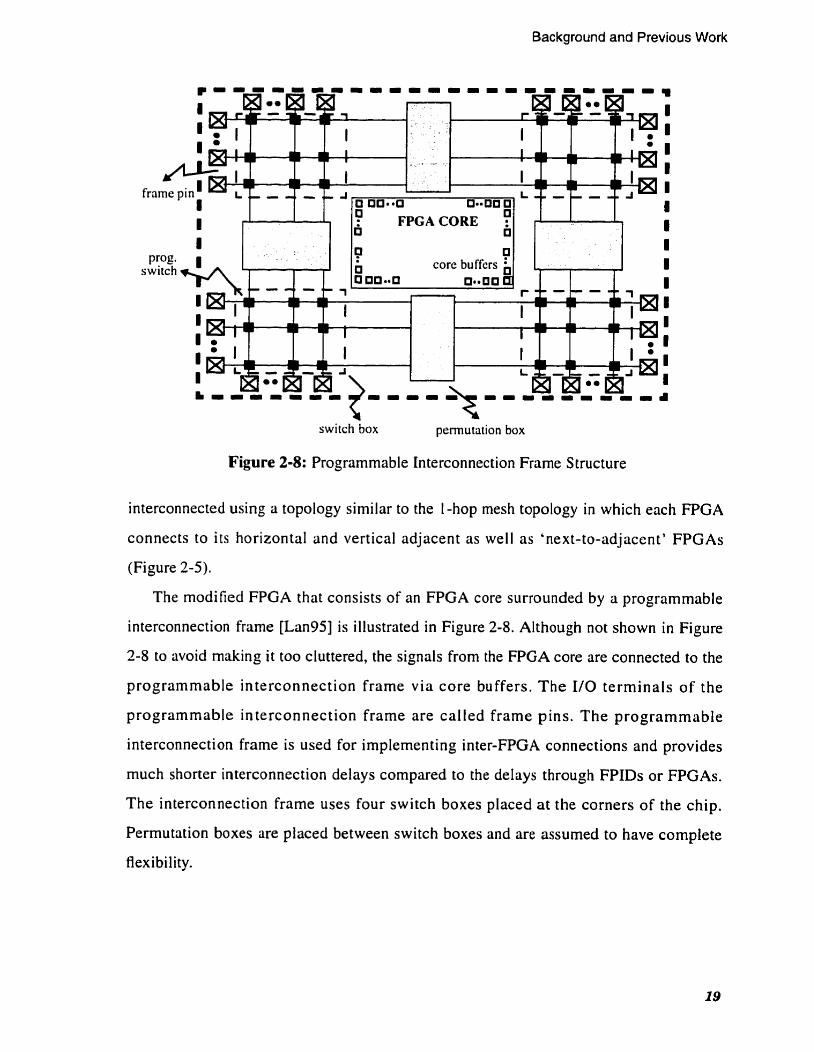
The modified FPGA that consists of an FPGA core surrounded by a programmable
interconnection frarne [Lang51 is illustrated in Figure 2-8. Although not shown in Figure
2-8 to avoid making i t too cluttered, the signals from the FPGA core are connected to the
programmable interconnection frame via core buffers. The I/O terminals of the
programmable interconnection frame are called frame pins. The programmable
interconnection frame is used for implementing inter-FPGA connections and provides
much shorter interconnection delays compared to the delays through FPIDs or FPGAs.
The interconnection frame uses four switch boxes placed at the corners of the chip.
Permutation boxes are placed between switch boxes and are assurned to have complete
flexibility.

Background and Previous Work
Netlist of gates and ( Hip Rops for input design 1
High level language ( description for input design )
Technology Ncrlist of CLBs Hardware mapping compiler
I
1 Panitioning into multiple FPGAs
Board-lcvcl FPGA placcmcnt t 4
Intcr-FPGA routing
Pin assignment, placement and routing within individual FPGAs
6 - Configuration bit stream gcneration for FPGAs and FPIDs
Figure 2-9: The Design Flow for MFSs
Experimental results show that the exact segmented FPMCM architecture gives one to
two orders of magnitude higher logic density and over a factor of two higher speed
compared to contemporary MFSs implemented on advanced PCBs.
2.2 CAD Flow for Multi-FPGA Systems
The steps needed to map a large design on to an MFS are described in this section. The
design flow is illustrated in Figure 2-9. The input design rnay be available as a huge flat
netlist of logic gates and flip fiops, as in the case of logic emulation and rapid prototyping.
Alternatively, it may be in the form of a high level Ianguage description, as in the case of
FPGA-based custom computing machines. The input description is mapped into a netlist
of configurable logic blocks (CLBs) of the FPGAs used [Babb97, Hauc98bl. The

Background and Previous Work
remaining steps (partitioning, placement and routing) constitute the layout synthesis phase
and will be described here in the context of MFSs. Formal problem definitions, objective
functions, and algorithms for each of these steps can be found in any introductory book on
VLSI physical design automation [Sher95, San-961.
A review of hardware compilers that generate circuit netlists from behavioral or
structural hardware description languages is beyond the scope of this work, but good
references covering this topic are available in [Page9 1, Ga1195, Knap96J. Similarly,
detailed discussion of issues in technology mapping, intra-FPGA placement and routing
can be found elsewhere [Brow92, Betz971.
The first step in the layout synthesis phase is multi-way partitioning. It is defined as
follows: given an input circuit divide it into a minimum possible number of sub-circuits
such that the total number of connections between sub-circuits is minimized and the logic
and pin limits on each sub-circuit are satisfied. The main objective here is to rninimize the
total cut size, i.e. the total number of wires between the sub-circuits while satisfying the
FPGA logic and pin capacity constraints.
The next step is placement of each sub-circuits on a specific FPGA in the MFS. This is
defined as follows: given al1 the sub-circuits and their interconnection netlist, assign each
sub-circuit to a specific FPGA so as to minimize the total routing cost of inter-FPGA
connections. The objective here is to place closely connected sub-circuits in adjacent
FPGAs (if the architecture has some notion of adjacency) so that the routing resources
needed for inter-FPGA connections are minimized. The total routing cost of inter-FPGA
connections is architecture dependent.
Given the sub-circuit interconnection netlist and their placement on FPGAs in the
MFS, the next step is inter-FPGA routing. The routing path chosen for each net should be
the shortest path (use the minimum number of hops) and it should cause the least possible
congestion for subsequent nets to be routed.
The inter-FPGA routing step is followed by pin assignment, which decides the
assignment of inter-FPGA signals to specific UO pins in each FPGA. This is followed by

Background and Previous Work
placement and routing within each FPGA in the MFS. The last step is the generation of
configuration bit streams to program each FPGA and FPID (if any).
2.2.1 Alternate Approach
Instead of partitioning the technology rnapped netlist representing the input circuit, as
shown in Figure 2-9 and used in many existing systems [Babb97], an alternate approach
would be to partition the gate-level netlist, followed by placement and inter-FPGA
routing. The technology mapping is done for the gate-level sub-circuit assigned to each
FPGA before the pin assignment step. This approach is preferred by some researchers
[Hauc95] and used i n commercially availüble mapping tools from Quickturn Design
Systems [Quic98]. The advantage of this approach is that technology mapping for smaller
sub-circuits can be done much faster in parallel compared to the technology mapping for a
single large gate-level netlist. There is also some empirical evidence that this approach
results in significantly smaller cut sizes after biparti tioning using an improved FM-based
algori thm [Hauc95]. It is not clear, however, if similar reductions can be obtained for
multi-way partitioning using other algorithms. Quickturn's primary motivation for using
this approach is to reduce the technology mapping run times and not any potential
reductions in cut sizes [Chu98].
The main disadvantage of this approach is that there is no information at this level
about the 'final' critical paths in the circuit, and the logic block and interconnect delays
[Roy95]. Therefore. timing-driven partitioning and inter-FPGA routing cannot be
performed for an unmapped circuit because there is no information available on the final
critical paths in the circuit being mapped to an MFS. This is a major limitation because
opportunities for significant speed improvemeni may be Iost.
2.3 Layout Synthesis Tools
In this section, previous work on partitioning, placement, and inter-FPGA routing for
MFSs is reviewed, and the pin assignment issue is covered briefly.

Background and Previous Work
2.3.1 Partitioning
The partitioning problem for MFSs is different compared to that in layout synthesis of
VLSI systerns because of hard pin and logic capacity constraints for each partition. When
typical circuits are partitioned into currently available FPGAs, the partitions are usually
pin-limited, Le. al1 the available logic in the FPGA cannot be used due to lack of pins.
Hence the prirnary goal of the partitioner is to minimize the total number of pins used (the
total cut size) across al1 partitions. Partitioning into multiple FPGAs can be achieved
either by direct multi-way partitioning or by recursive bipartitioning. The former approach
usually gives superior results [Chou951 but is much harder compared to the latter approach
because bipartitioning is a well studied problem and widely used algorithms that give
good results in real world (commercial) CAD tools are available [Fidu82, Kris84, Hei1971.
Many multi-way partitioning algorithms developed for MFSs use minimization of the
total cut size as their primary objective [Woo93, Kuzn94, Chou951. The additional
objectives used are to make the partitioner timing-driven and routability-driven.
Timing-driven partitioning attempts to minimize the effects of partitioning on circuit
speed by preventing the critical paths in the circuit from traversing too many partitions
[Kim96, Roy951. Routability-driven partitioning attempts to produce partitions that lead to
successful inter-FPGA routing for the target MFS architecture. Obviously, to succeed in
this task, the partitioner needs to be aware of the topology of the target MFS architecture
[Hauc95, Kim96J.
The Fidducia and Mattheyses [Fidu821 graph bipartitioning algorithm (generally
referred to as FM) forms the basis of many multi-way partitioning algorithrns due to its
speed, efficiency and relatively easy implementation. It is an iterative improvement
algorithm that uses multiple passes. It staris with an initial random partition and during
each pass it attempts to reduce the cut size of the partition by moving cells from one
partition to the other. The ce11 to be moved is selected based on its gain, which is the
number by which the cut size would decrease if the ceIl is moved. In some cases, the gain
of a ceIl is negative, but it is still moved with the expectation that the move will allow the

Background and Previous Work
algorithm to 'escape out of a local minimum'. This feature is also referred to as 'hi11
climbing' in the literature.
In [Kuzn93, Kuzn941 a modified form of the FM algorithm, further enhanced by using
functional replication to minimize cut size in each partition, is used to for bipartitioning.
This algorithm is used in a recursive manner to partition a design into minimum possible
number of homogeneous FPGAs or into a set of minimal cost heterogeneous FPGAs.
The multi-way partitioning algorithm proposed in [Woo93] also uses an iterative
improvement method (like FM) but differs in the way it selects a ce11 to move and the
manner in which i t moves the cell.
An efficient algorithm for multi-way partitioning of huge circuits used in logic
emulation was proposed in [Chou95]. It first applies a fast clustering scheme called the
local ratio cut to produce initial partitions. It then uses a set covering approach to improve
the initial partitioning and remove any inefficiencies that may be introduced during
clustering. Compared to a recursive FM algorithm, this algorithrn reduced the number of
FPGAs required by 4 1 % and the run time by 86% for partitioning a circuit containing 160,
000 gates (assuming FPGA logic and pin capacities of 2700 gates and 184 I/O pins).
A routability and performance-driven partitioning algorithm is presen ted in [Kirn96].
In the tirst phase, clustering-based partitioning is performed whose objective function is
the weighted sum of the cut size and the maximum delay. This is followed by a partition
improvement step that is based on the gain (cut size reduction) of moving a ce11 from one
FPGA to the other. In the second phase, inter-FPGA routing is performed and the existing
partitions are improved to obtain 100% routability for the target MFS architecture. Here, if
the inter-FPGA routing attempt fails, then the cells are moved between partitions in an
attempt to obtain routing completion.
Many other techniques like the spectral method [Chan95], simulated annealing
[Roy95], and partitioning based on design hierarchy [Behr96], have been proposed for
multi-way partitioning in MFSs.

Background and Previous Work
Part: A Partitioning Tool Developed for the TM-1 MFS An example of a practical rnulti-way partitioning tool is Part, which was originally
developed for the Transmogritier- l (TM- 1 for short) MFS [Ga1194]. The term 'practical'
indicates that the tool has been used with an existing MFS (the TM-1) and real circuits
have been partitioned and implemented on the TM-I using this tool.
Pnrt is based on the FM algorithm with extensions for multi-way partitioning and
timing-driven pre-clustering [Shih92]. The basic FM algorithm gives much improved
results when combined with a set of techniques such as pre-clustering and utilization of
higher-level gains [Hauc95, Kris941.
Clustering before partitioning reduces the run time and gives better quality results.
Since many nodes are replaced by a single cluster, the algonthm runs much faster because
i t has fewer nodes to partition. The FM algorithm is a global algorithm that optimizes the
macroscopic properties of the circuit and may overlook more local concerns. An
intelligent clustering algorithm can perform good local optimization, complementing the
global optimization properties of the FM algorithm. Purt uses a timing-driven
pre-clustering algorithrn, similar to that proposed in [Shih92], to reduce the cut size as
well as the delay obtained after bipartitioning. Timing-driven partitioning is accomplished
by modifyinp the FM algorithm such that when selecting a cluster to be moved, the
algorithm tries to select a cluster to move that prevents the critical paths from traversing
across too many partitions. Notice that the timing-driven feature of Part will be lost after
the first cut if we use it for implementing multi-way partitioning through a recursive
bi-partitioning approach.
We could not compare multi-way partitioning results obtained using Part to the other
partitioning algorithms because none of them give results for the circuits and FPGA logic
and pin capacities that we use. Another important point to note is that while minimizing
the cut size during partitioning is important, a small variation in the cut size is acceptable
as long as the partitioned netlist is routable on a given MFS. Overall, we believe that Pnrt
gives reasonably good results because it uses pre-clustering combined with the FM
algori thm.

Background and Previous Work
2.3.2 Placement
Following circuit partitioning the placement tool assigns sub-circuits to specific
FPGAs such that inter-FPGA routing costs and critical path delays are minimized. This
task can be done simultaneously with partitioning [Roy%, Kim961 or as a separate step
[Babb97]. Well known algorithms like simulated annealing [Shah911 have been used for
placement on MFSs [Roy%, Babb971.
The placement task is trivial for some architectures such as the partial crossbar, where
any random placement is acceptable because the number of wires between any pair of
FPGAs is the same.
A Force-Directed Placement Algorithm Force-directed placement algorithms have been used for board-level placement of IC
chips [Quin79, GotoSI] and could potentially be used for placement i n the mesh
architectures. Force-directed algorithms are rich i n variety and differ greatly i n
implementation details [Shah9 11. The common element in these algorithms is the method
used to calculate the location where a module (sub-circuit) should be placed on the target
two-dimensional array to achieve its ideal placement. The algorithrns operate on the
physical analogy of a system of masses connected by springs, where the system tends to
rest in its minimum energy state with minimum combined tension from al1 the springs.
Consider any given initial placement. Assume that the modules that are connected by
nets exert an attractive force on each other. The magnitude of the force between any two
modules is directly proportional to the distance between them and the number of
connections between them. Since each module is usually connected to many other
modules, it will be pulled in different directions by different modules. If the modules in
such a system were allowed to move freely, they would move in the direction of the force
until the system achieves equilibrium with zero resultant force on each module.
Suppose a module Mi is connected to j other modules. Let Cg represent the number of
connections between the module Mi and the module Mi. The coordinates for the zero force
target point for the module Mi can be derived as follows:

Background and Previous Wotk
A version of the force-directed placement algorithm from [Shah9 11 is illustrated in
Figure 2- 10. This is an iterative algorithm that starts with an initial placement solution that
is randomly generated. Then a module witli the highest connectivity (seed module) is
selected and its target point computed using the above equations.
The inner while loop of the algorithm is executed while the end-ripple flag is false. If
the computed target point of a module is the sorne as its present location or is vaccrnt, then
the end-rippk flag is set to trice, dort-cortnt is set to zero and module is assigned to the
computed position and locked.
If the target point is occrcpied, the algorithm uses ripple moves in which the selected
module is moved to the computed target point and locked. The module displaced is
selected as the next seed module to be moved, e d - r i p p k is set to false and clbort-count is
set to zero. When a module is moved to its target point, it is necessary to lock i t for the rest
of the current iteration in order to avoid infinite loops, which can occur i f two modules
compete for the same target point.
If the computed target point is occupied and locked, then the selected module is moved
to nearest vacant location, abort-cowzt is incremented and end-ripple is set to true. If
crbort-cowtt is less than nbort-linzit, then the next seed module is selected and the same
iteration continues. Otherwise, al1 locations are unlocked, iteratiorz-count is incremented,
and a new iteration is started.
The process of selecting seed modules in the order of their connectivity and attempting
to place them in their ideal locations continues until the iterution-hzit is reached. The
placement available at this point is the final placement solution. In this algorithm, there is
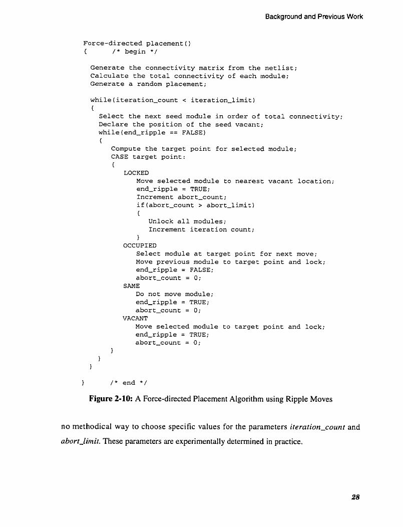
Background and Previous Work
Force-directed placement() C / * begin * /
Generate the connectivity matrix from the netlist; Calculate the total connectivity of each module; Generate a random placement;
while(iteration-count < itexation-limit) { Select the next seed module in order of total connectivity; Declase the position of the seed vacant; while(end-ripple == FALSE) (
Compute the target point for selected module; CASE target point: (
LOCKED Move selected module to nearest vacant location; end-ripple = TRUE; Increment abort-count; if(abort-count > abort-limit) (
Unlock a l1 modules; Increment iteration count;
1 OCCUPTED
Select module at target point for next move; Move previous module to target point and lock; end-ripple = FALSE; aboxt-count = 0;
SAME Do not move module; end-ripple = TRUE; abort-count = 0;
VACANT Move selected module to target point and lock; end-ripple = TRUE; abort-count = 0;
1 1
1
1 / * end * /
Figure 2-10: A Force-directed Placement Algorithm using Ripple Moves
no methodical way to choose specific values for the parameters itemfion-corint and
nbort-iimit. These parameters are experimentally determined in practice.

Background and Previous Work
Figure 2-1 1: Inter-FPGA Routing in a 4-way Mesh
2.3.3 Inter-FPGA Routing
The inter-FPGA router determines the routing path for each inter-FPGA net. The
router could use direct connections between two FPGAs or i t may use intermediate
FPGAs and FPIDs, depending upon the routing architecture and wire availability. The
choice of speciftc pins and wires (from a group) to use for routing a net is left to the pin
assignment step. For exnmple, consider a net that connects FPGAs O and 8 in the 4-way
rnesh shown in Figure 2- I I . Three of the many possible paths for routing the net are
shown using dashed lines. The final path chosen will depend upon the availability of wires
and the congestion encountered in each path.
Ideally the router should use on1 y one hop for each source-to-sink connection in al1 the
nets so that the usage of FPGA pins and the delay is minimized. Simultaneously, i t should
also balance the usage of routing resources to ensure routing completion. This may be
difficult in practice because the amount of routing resources in an MFS is fixed. The
minimization of pins used in routing a net rather than any geometric distance metric
makes the inter-FPGA routing problem unique compared to routing in ASICs or FPGAs.
Routing cornpletion is the primary goal, because in the case of routing failure the
partitioning step has to be repeated and the design may require more FPGAs to fit. Once
the primary goal seerns achievable, secondary goals such as maximizing the circuit speed
can be addressed. Many routing algorithms for different MFS routing architectures have
been proposed and will be reviewed briefly in this section.

Background and Previous Work
Routing Algorithms for the Partial Crossbar
Due to its importance in commercial logic emulators, the inter-FPGA routing problem
for the partial crossbar architecture has been investigated by several researchers [Butt92,
Slim94, Makgsa, Mak95b. Lin971. Recall from Section 2.1.3 and Figure 2-3(b) that the
partial crossbar has no direct connections between FPGAs and any connections between
FPGAs must go through FPIDs. Given a post-partition inter-FPGA netlist, the routing
problem reduces to choosing a specific FPID for routing each net such that al1 the nets
route.
The earliest proposed algorithms [ButtsgZ, Slim941 are based on greedy heuristics. In
this case, for routing each net the first available FPID that has connections to al1 the net
terminais (FPGAs) is selected. Because of the greedy approach these algorithms may not
find a routing solution in some cases where a solution exists.
Optimal algorithms for routing two-terminal nets were proposed by Chan [Chan931
and Mak [Mak95a]. These algorithms guarantee 100% routing completion for al1
two-terminal nets. It is also shown that the multi-terminal net routing problem for partial
crossbar is NP-complete. Unfortunately, post-partition netlists for real circuits almost
always contain multi-terminal nets and there is no guarantee of routing completion even if
optimal algorithms for two-terminal nets are used as part of the solution.
One way of routing multi-terminal nets on a partial crossbar is to break each net into a
set of two-terminal nets and route the resulting two-terminal nets using the proposed
optimal algorithms. Such an approach is proposed in [MakgSb] and an algoritlm for
decomposing multi-terminal nets into a set of two-terminal nets is presented. The
decomposition problem is modeled as a bounded-degree hypergraph-to-graph
transformation problem where hyperedges (representing multi-terminal nets) are
transformed to spanning trees of only two terminal nets. A network flow-based algorithm
is suggested that determines if there is a feasible decomposition so that FPGA I/O pin
capacities are not violated due to decomposition, and gives one if it exists. This is a deeply
flawed and impractical approach for the following reasons: first, the number of FPGA Y0
pins needed after decomposition wiil drastically increase, especially for higher fanout
nets. Decomposing one n-terminal net into a set of two-terminal nets requires n-2 extra
Background and Previous Work
pins. FPGA pins are the most scarce resource in MFSs and extra pins for decomposition
may not be available. Second, decomposition rnay lead to routing paths between source
and sinks that consist of multiple hops, thus greatly increasing the delay of the circuit
being implemented. It is much better to use a method that uses a single FPID to directly
route a multi-terminal net while trying to minimize congestion for subsequent nets to be
routed.
A combination of heuristic and exact algorithms for two-terminal and multi-terminal
net routing is presented in [Lin97]. In this two-phase approach, a fast (linear tiine
complexity) heuristic algorithm is used first, the exact algorithm is called only if the
heuristic fails to provide routing completion. The heuristic algorithm routes nets based on
the order of their fanout, i.e. the highest fanout nets first and two-terminal nets last. For a
given net, an FPID is selected that has wires available for connecting to al1 the net
terminais (FPGAs) and has the most unused pins across al1 FPIDs i n the system, Le. the
most lightly used FPID. This minirnizes congestion and increases the chance of
successfully routing subsequent nets. The authors also report a further modification of this
heuristic that gives improved results.
In the exact algorithm, the routing problem (for any fanout) is formulated as a linear
programming problem and solved. This exact algorithm will tind a solution if one exists.
however it rnay take exponential time. To deal with the large and sparse matrices required,
which existing solvers could not handle, the authors developed their own linear
programming solver.
These heuristic algorithms were compared with the heuristic given in [Varg93] and
gave superior results for synthetic netlists. The partial crossbar used had 8 FPGAs and
routing was performed for different values of the number of pins per subset ranging from 1
to 32 in variable increments. On the more difficult routing problems, the exact algorithm
gave better results (measured by the percentage of nets routed) compared to the heuristic
algorithms.
A limitation of studies discussed above for routing in partial crossbars (with the
exception of [Butr92]) is that they used synthetic netlists instead of real circuits. It is

Background and Previous Work
possible to make the algorithm overly complicated in order to route synthetic netlists, as in
the case of the exact algorithm proposed in [Lin971 and multi-terminal net routing
approach proposed in [MakgSb]. If post-partition netlists of real circuits are used, it would
give a much better idea of what algorithms work best in practice.
Topology Independent Routing Algorithms
Inter-FPGA routing tools capable of handling arbitrary MFS topologies have been
proposed [Selv95, Kim96J. The inputs to such tools are post-partitioning-and-placement
netlists and routing architecture topology descriptions.
In [Selv95] a topology independent pipelined routing and scheduling (TIERS)
algorithm is presented for the Virtuai Wires system. Recall from Section 2.1.2 that in the
Virtual Wires scheme several logical wires between sub-circuits are multiplexed on a
single physicai wire between FPGAs. The inter-FPGA routing phase in this case should
not only specify the path for routing each net but also the time slice in which the
connection is established, which is determined by the scheduling algorithm. For routing,
which is our main interest here, the well known maze routing algorithm is used and its
flrxibility is exploited to handle any arbitrary MFS topology. The MFS is represented as a
graph whose nodes are FPGAs. To find the shortest path for routing a net, breadth first
search is pedormed starting from the source FPGA and stopping once the target FPGA is
reached. The TIERS algorithm also identifies critical nets and gives them higher priority
to achieve as much as a factor of 2.5 speed improvement over prior work [Babb93].
A different approach towards topology independent routing is adopted in [Kim96]. For
each topology, al1 possible routing paths (patterns) between every pair of FPGAs are
stored. To minimize inter-FPGA routing delays, only paths of length one or two hops are
considered. When routing each net, one of several stored paths is chosen based on a cost
function that attempts to minimize the congestion and the path length. To simplify path
generation and storage, a11 multi-terminal nets are split into a set of two-terminal nets and
routed independently. This, however, introduces some inefficiencies as discussed in the
previous section when reviewing the routing algorithm in wak95bl. This algorithm was
used to map real circuits to several different architectures.

Background and Previous Work
2.3.4 Pin Assignrnent
The pin assignment step chooses the specific wires and pins to use for each connection
given by inter-FPGA router. For example consider the three possible routing paths shown
i n Figure 2-1 1 for a net connecting FPGA O to 8. Assume that the path through
intermediate FPGAs 3, 4, and 5 is chosen. The pin assignment step will choose specific
wire segments (and FPGA pins) for connecting each pair of FPGAs in the path, i.e. (0,3),
(3,4), (43 ) and (5,8). Notice that each line between the FPGAs i n Figure 2-1 1 actually
represents a group of wires connecting distinct FPGA pins.
The pin assignment has no effects on inter-FPGA routing resources and only affects
placement and routing for individual FPGAs and routing for FPIDs. In many existing
systems [Lewi98, Quic981 the pins are assigned randomly within the constraints imposed
by the inter-FPGA router. This has the effect of randomly locking individual FPGA pins
before placement and routing, which may lead to increased consumption of routing
resources within the FPGA. For the past few years, however, leading FPGA vendors like
Xilinx and Altera have enhanced their FPGA architectures and mapping tools to handle
pin locking without unduly adverse impact on either the routability and speed of FPGAs
or the run tirne for FPGA place and route [Trim95, Hei196J. The architectural
improvement in the Xilinx 4000 family of FPGAs is the addition of extra routing
resources, including long lines that span the length of the chip, on the periphery of the
FPGA chip. These extra routing resources could provide fast arbitrary pin-CO-pin
connections within FPGAs. Given these improvements, pin assignment algorithms such as
those proposed in [Hauc95] may or may not give better ruii time and delay results
compared to random pin assignments. The only way to decide would be to map real
circuits to MFSs (that utilize a state-of-the-art FPGA) using both these approaches, and
compare the run times and post-mapping critical path delays obtained.
A review of existing MFSs and the different routing architectures and mapping CAD
tools used was presented in this chapter. These systems were grouped into three main

Background and Previous Work
categories based on their iopology and the interconnect devices used: Iinear arrays,
meshes, and architectures that use programmable interconnection chips. The relevant MFS
architecture research studies were considered, which show that the partial crossbar is one
of the best existing architectures. The design fiow for mapping circuits to MFS
architectures was described and the various mapping tools for the layout synthesis tasks in
the design flow (partitioning, placement, and inter-FPGA routing) were reviewed.
Although many MFSs have been proposed and built, there has been very little research
work on comparing di fferen t MFS routing architectures and evaluating their effectiveness
in implementing real circuits. This problem is addressed in this dissertation by using an
experimental approach for comparing and evaluating different MFS routing architectures
using real benchmark circuits. The details of al1 the architectures exploi-ed are described in
the next chapter.
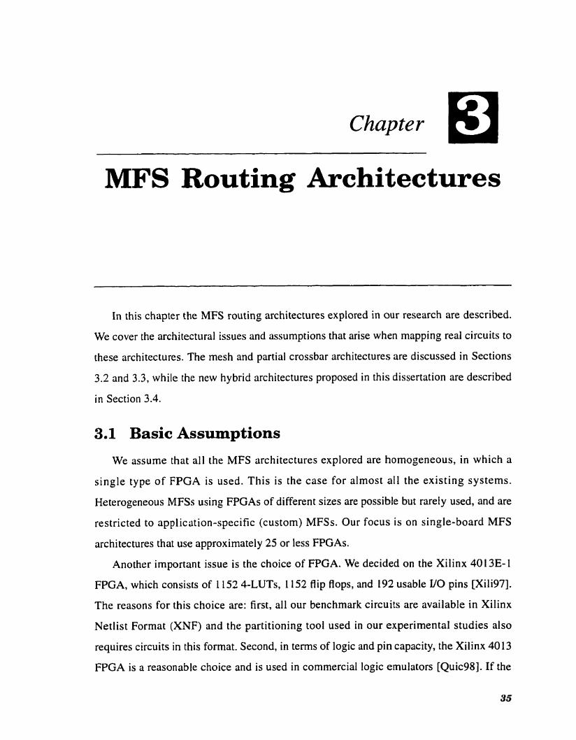
MFS Routing Architectures
In this chapter the MFS routing architectures explored in our research are described.
We cover the architectural issues and assumptions that arise when mapping real circuits to
these architectures. The mesh and partial crossbar architectures are discussed in Sections
3.2 and 3.3, while the new hybrid architectures proposed in this dissertation are described
in Section 3.4.
Basic Assumptions
We assume that al1 the MFS architectures explored are homogeneous, in which a
single type of FPGA is used. This is the case for almost al1 the existing systems.
Heterogeneous MFSs using FPGAs of different sizes are possible but rarely used, and are
restricted to application-specific (custom) MFSs. Our focus is on single-board MFS
architectures that use approximately 25 or less FPGAs.
Another important issue is the choice of FPGA. We decided on the Xilinx 4013E-1
FPGA, which consists of 1152 4-LUTs, 1152 flip flops, and 192 usable Il0 pins [Xili97].
The reasons for this choice are: first, al1 Our benchmark circuits are available in Xilinx
Netlist Format (XNF) and the partitioning tool used in Our experimental studies also
requires circuits in this format. Second, in terms of logic and pin capacity, the Xilinx 40 13
FPGA is a reasonable choice and is used in commercial logic emulators [Quic98]. If the

MFS Routing Architectures
I I
I 1 , FPGA FPGA FPGA 2 6 ' 7 8
I 1 1
Figure 3-1: Mesh Architectures: (a) 4-way Mesh (b) 8-way Mesh (c) 4-way Torus (d) 8-way Torus
-
FPGA used is too large, many of the benchmark circuits may fit into a single FPGA and
prevent the study of MFS architectures. If it is too small, the circuit partitioning would
result in a large number of FPGAs that rnay not fit into a single board, violating our
assumption about single-board MFS architectures. We conjecture that inter-FPGA netlists
for larger benchmark circuits mapped to MFSs using larger FPGAs (compared to the
Xilinx 40 13 FPGA) would exhibit similar behavior. Therefore the architectural results
obtained in O u r research would also apply to larger circuits and MFSs using larger FPGAs.
FPGA O
C
- ,
I I
FPGA 3
2 FPGA 4
FPGA. 1
-
FPGA 5
FPGA 2
FPGA 3
FPGA 4
I I I
FPGA 5 -
-
I
FPG A 6
- FPGA 7
. FPGA 8
MFS Routing Architectures
4-way and 8-way Mesh Architectures
The simplest mesh topology is a 4-way rnesh as illustrated in Figure 3- 1 (a). Each
FPGA is connected to its horizontal and vertical adjacent neighbours. The number of
wires connecting adjacent FPGAs depends upon the number of I/O pins available per
FPGA. The Xilinx 4013 FPGA has 192 usable VO pins. We reserve four of these pins for
routing global nets frequently encountered in circuits such as dock and reset, leaving 188
pins in each FPGA for inter-FPGA connections. Hence each edge in Figure 3-l(a)
represents 47 ( 188 1 4) wires.
A variation of this basic mesh topology is the 8-way mesh as shown in Figure 3-l(b).
Each FPGA is connected to its horizontal. vertical, and diagonal adjacent neighbours and
each edge in Figure 3- 1 (b) represents 23 wires (1 1). Notice that since 1 88 is not evenly
divisible by 8 (remainder is 4). only 184 pins out of 192 pins per FPGA are used for
inter-FPGA connections in the 8-way mesh. The remaining 8 lines can be used as global
lines (each global line connects to al1 FPGAs) for routing very high fanout nets. Notice
that the number of global lines in the 4-way mesh (4) is different from that in the 8-way
mesh (8). This small difference in the number of global lines is unavoidable and will occur
for other architectures as well, but has no impact on architectural results.
One major drawback of 4-way and 8-way meshes is that the edges in FPGAs that lie
on the periphery of the array cannot be utilized for inter-FPGA routing. For example in
Figure 3-l(b) only three out of eight edges emanating from FPGA O are connected to
neighbouring FPGAs implying that only about 38% of the VO pins are connected to other
FPGAs, the rest being wasted. When implementing a large circuit on this array, the only
way these edges can be used is for circuit I/0 signals. However al1 circuits usually do not
use a large number of VO signals and hence these edges will be wasted and will lead to
inefficiency. Preliminary experiments confirmed this and hence we do not present any
results for these mesh topologies.
Instead, we use a toms topology that provides enough FPGA UO pins for circuit V 0
signals and at the same time avoid waste of pins. As shown in Figure 3-1 (c) and (d), the
unused edges on the peripheral FPGAs are wrapped around in horizontal and vertical

MFS Routing Architectures
directions and are connected to FPGAs on the opposite side of the array. For example,
FPGA O in Figure 3-l(c) is connected to FPGAs 2 and 6. Note that in 8-way toms we use
only horizontal and vertical wrap around, with no wrap around in diagonal directions. The
reason is that if we use diagonal wrap around, some edges emanate and end on the same
FPGA, which does not help inter-FPGA routing in any way. In each FPGA, a certain
number of pins are reserved for circuit I l0 signals, the exact number used in our
experiments is dictated by the number of 110 signals in the circuit being mapped.
3.3 Partial Crossbar Routing Architecture
Recall frorn Section 2.1.3 that the partial crossbar uses a number of small crossbars to
provide interconnections between multiple FPGAs. Also recall from Figure 2-3 that in a
partial crossbar the pins in each FPGA are divided into N subsets, where N is the number
of FPIDs in the architecture. AI1 the pins belonging to the same subset number in different
FPGAs are connected to a single FPID. Note that any circuit I l 0 signals will have to go
through FPIDs to reach FPGA pins. For this purpose, 50 pins per FPID are reserved for
circuit UO signals in Our experiments.
The number of pins per subset (P,) is a key architectural parameter that determines the
number of FPIDs (N,) needed and the pin count of each FPID (P,). Given the values of the
number of pins per subset (P,), the nurnber of FPGAs (Nr) in the partial crossbar and the
number of I/0 pins in each FPGA (Pf), N p d P, are given by [Butt92]:
The extremes of the partial crossbar architecture are illustrated in Figure 3-2 by
considering a system with four Xilinx 4013 FPGAs (192 usable VO pins). A Pt value of
192 would require a single 768-pin FPID (Figure 3-2(a)) that acts as a full crossbar and a
Pt value of 1 will require 192 4-pin FPIDs (Figure 3-2(b)). Both of these cases are
imprac tical.
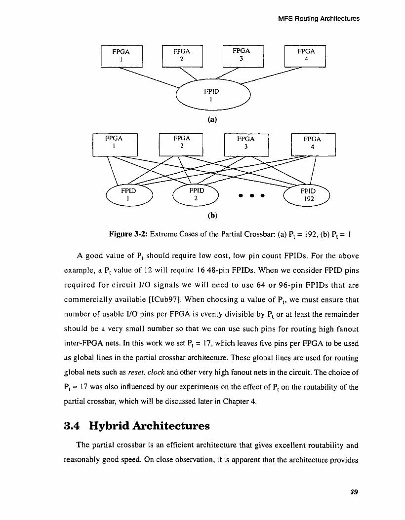
MFS Routing Architectures
FPGA FPGA FPG A FPGA I 2 3 4
(b)
Figure 3-2: Extreme Cases of the Partial Crossbar: (a) P, = 192, (b) Pt = 1
A good value of P, should require low cost, low pin count FPIDs. For the above
example, a P, value of 12 will require 16 48-pin FPIDs. When we consider FPID pins
required for circuit I I0 signals we will need to use 64 or 96-pin FPIDs that are
commercially ûvailable [ICub97]. When choosing a value of Pt, we must ensure that
number of usable I/O pins per FPGA is evenly divisible by P, or at least the remainder
should be a very small number so that we can use such pins for routing high fanout
inter-FPGA nets. In this work we set Pt = 17, which leaves five pins per FPGA to be used
as global lines in the partial crossbar architecture. These global lines are used for routing
global nets such as reset, dock and other very high fanout nets in the circuit. The choice of
P, = 17 was also influenceci by our experiments on the effect of P, on the routability of the
partial crossbar, which will be discussed later in Chapter 4.
3.4 Hybrid Architectures
The partial crossbar is an efficient architecture that gives excellent routability and
reasonably good speed. On close observation, it is apparent that the architecture provides

MFS Routing Architectures
FPGA 1 F PGA 2 FPGA 3 A B C D A B C D A B C D
,-
1 -
I L - T
FPGA 4 FPGA 5 - FPGA 6 A B C D A B C D A B C D
Figure 3-3: The HTP Architecture
more routing flexibility than necessary, which cornes at a cost of extra FPID pins. For
example, consider two-terminal net routing in the partial crossbar; al1 such nets have to
use an FPID to connect two FPGAs. If the architecture has direct connections between
FPGAs, no FPIDs would be needed for routing certain two-terminal nets, thus saving
FPID pins. The direct connections would also be faster than the connections through
FPIDs.
These observations motivated us to propose new hybrid MFS routing architectures that
have the flexibility of the partial crossbar and use a mixture of both programmable and
hardwired connections. The hardwired connections are most suitable for routing
two-terminal nets that connect adjacent FPGAs and can also be exploited to improve the
speed performance. The programmable connections are best suited for routing
multi-terminal nets. A key issue in the hybrid architectures is the choice of topology for
the hardwired connections between FPGAs. We chose and explored three topologies for
hardwired connections in this dissertation. The motivations for these choices are presented
below, dong with the architecture descriptions.
3.4.1 Hybrid Torus Partial-Crossbar
The first newly proposed hybrid routing architecture is the Hybrid Torus
Partial-Crossbar (HTP). The motivation behind this architecture is to combine the locality

MFS Routing Architectures
of inter-FPGA connections, provided by the mesh architecture, with the routing flexibility
provided by the partial crossbar. This locality will lead to easier manufacturability by
reducing the board-level wiring complexity.
The UO pins in each FPGA are divided into two groups: hardwired and programmable
connections. The pins in the first group connect to FPGAs and the pins in the second
group connect to FPIDs. The FPGAs are connected to each other in a 4-way torus
topology and the FPGAs and FPIDs are connected i n exactly the same rnanner as in a
partial crossbar, as illustrated in Figure 3-3. An HTP architecture that consists of six
FPGAs and four FPIDs is shown. The pins assigned for programmable connections are
divided into four subsets A, B, C, and D. The pins from different FPGAs belonging to the
same subset are connected using a single FPID. Since the circuit VO signals will have to
go through the FPTDs to reach FPGA pins, 50 pins per FPID are reserved for circuit If0
signals.
A key architectural parameter i n the HTP architecture is the percentage of
programmable connections, Pp. It is defined as the percentage of each FPGA's pins that are
connected to FPIDs, with the remainder hardwired to other FPGAs. If Pp is too high it will
lead to increased pin cost because more programmable connections are required, which
implies more FPID pins. If Pp is too low it will adversely affect routability. If PI, is 0% the
HTP architecture degrades to a 4-way torus with no FPIDs used. If Pp is 100% the HTP
architecture degrades to a standard partial crossbar. A key issue we address later (in
Chapter 5) is the best value of PI, for obtaining minimum cost and good routability.
Notice that the parameter P, also applies to the programmable connections i n the
HCGP (another hybrid architecture introduced in the next Section). For the same reasons
as in the partial crossbar (given in Section 3.3), we chose Pt = 14 for the HCGP
architecture i n our experiments. Also, the number of global lines used in the HTP
architecture depends upon the MFS size (the number FPGAs used) and the parameters Pp
and Pt. In our experiments, the number of global lines used for the HCGP architecture
varied from 5 to 15. Recall from Section 3.3 that the number of global lines for the partial
crossbar is 5 corresponding to Pt = 17. The different values for number of global lines used

MFS Routing Architectures
Figure 3-4: The HCGP Architecture
in HCGP is due to the fact that the number depends upon both Pp and P, instead of just P,
as in the partial crossbar architecture. This discussion about the value of Pt and the number
of global lines used also applies to the remaining hybrid architectures presented in this
chapter.
3.4.2 Hybrid Complete-Graph Partial-Crossbar
The second newly proposed architectures is called the Hybrid Complete-Graph
Partial-Crossbar (HCGP). The HCGP architecture for four FPGAs and three FPIDs is
illustrated in Figure 3-4. As in HTP architecture, the Il0 pins in each FPGA are divided
into two groups: hardwired connections and programmable connections. The pins in the
first group connect to other FPGAs and the pins in the second group connect to FPIDs.
The FPGAs are directly connected to each other using a complete graph topology, which
means that each FPGA is connected to every other FPGA. The connections between
FPGAs are evenly distributed, which implies that the number of wires between every pair
of FPGAs is the saine. The FPGAs and FPIDs are connected in exactly the same manner
as in a partial crossbar. Since any circuit I/O signals will have to go through FPIDs to
reach FPGA pins, 50 pins per FPID are reserved for circuit VO signals.
The direct connections between FPGAs can be exploited to obtain reduced cost and
better speed. For example, consider a net that connects FPGA 1 to FPGA 3 in Figure 3-4.

MFS Routing Architectures
FPGA 4 FPGA 3
Figure 3-5: Mu1 ti-terminal Net Routing: (a) Without an FPID (b) Wi th an FPID
If there were no direct connections (as in the partial crossbar), we would have used an
FPID to connect the two FPGAs. This will cost extra delay and two extra FPID pins. A
natural question to ask is: why not dispense with FPlDs and just use FPGAs connected as
a completely connected graph as investigated i n [Kim96]? The answer is that routing
multi-terminal nets in a hardwired FPGA-only architecture is expensive in terms of
routability because in such an architecture a multi-terminal net requires many extra pins in
the source FPGA. For example, as illustrated in Figure 3-5(a), two extra FPGA pins are
used for routing a fanout 3 multi-terminal net. Since extra pins are a very scarce resource
on an FPGA this has an adverse effect on the routability of FPGA-only architectures. On
the other hand, if we use an FPID for routing the same muiti-terminal net, we do not need
even a single extra FPGA pin, other than the FPGA pins needed to access the source and
sinks of the net as shown in Figure 3-5(b).
The complete graph topology for the hardwired connections provides good routing
flexibility, because for connecting any pair of FPGAs direct connections beiween them
can be used, and once they are exhausted, any FPGA outside the pair can be utilized for a
two-hop connection, provided it has enough 'free' pins for routing.

MFS Routing Architectures
A B C A B C A B C A B C 8
l
Figure 3 4 : The HWCP Architecture
3.4.3 Hardwired-Clusters Partial-Crossbar
The motivation behind this architecture is to combine the routability and speed of the
HCGP wi th easier manufacturability. AI1 the connections in the HCGP architecture are
non-local which leads to excessive board-level wiring complexity. Providing more local
connections would mitigate this problem (recall the motivation behind the design of the
TM-2 from Section 2 .1 .3 ) . The Hardwired-Clusters Partial-Crossbar (HWCP)
architecture has the potential to provide good routability, speed, and manufactunbility.
An example of the HWCP architecture using six FPGAs and three FPIDs is illustrated
in Figure 3-6. The FPGAs are grouped into clusters whose size is represented by a
parameter called the cluster size (C,). In Figure 3-6 Cs = 2, which implies three clusters.
The pins in each FPGA are divided into two groups: hardwired and programmable
connections. The pins in the first group connect to the other FPGAs within each cluster
and the pins in the second group connect to FPIDs. Al1 the FPGAs within each cluster are
connected to each other in a complete graph topology. In Figure 3-6 the pins assigned for
programmable connections are divided into three subsets A, B, and C. The pins from
different FPGAs belonging to the same subset are connected using a single FPID. As in
the HCGP architecture, the percentage of programmable connections (Pp) is a key
parameter in HWCP.
The intra-cluster connections for Cs = 3 and Cs = 4 are illustrated in Figure 3-7(a) and
Figure 3-7(b) respectively. Notice that the MFS size in the HWCP architecture is restricted

MFS Routing Architectures
FPGA 1 FPGA 2
FPGA 3 I A B C l (a)
r
FPGA 1 FPGA 2
A B C A B C
FPGA 3 , FPGA 4
A B C A B C
Figure 3-7: Different Cluster Sizes for HWCP (a) Cs = 3 (b) Cs = 4
to be a multiple of Cs. In this research the HWCP architecture was explored for Cs values
3, 3, and 4.
In addition to reducing board-level wiring complexity in single-board systerns, the
HWCP is suitable for larger MFS sizes. It lends itself to hierarchical irnplementations of
large MFSs using FPGAs distributed across multiple boards, with one or two clusters and
a fraction of al1 the FPIDs, assigned to a single board.
3.5 Summary
The MFS routing architectures that are explored in this dissertation were described in
this chapter. The intuitive ideas that led to the proposal of the new hybrid architectures
were discussed. The proposal of a new MFS architecture is relatively easy, but presenting
convincing evidence that demonstrates its effectiveness for reai circuits is a difficult and
time consuming task.
In this dissertation, we developed a framework for experimental evaluation of MFS
routing architectures. Real benchmark circuits are mapped to different routing
architectures to evaluate the 'goodness' of each architecture relative to the others. This
experimental framework is the focus of the next chapter.

CAD Tools and Experimental Evaluation
Framework
A wide range of MFS routing architectures were presented in the previous two
chapters. To evaluate and compare different architectures, an experimental framework is
required that enables mapping of real circuits to different architectures. The framework
developed in this research is the focus of this chapter. An overview of the experimental
procedure used for mapping a circuit to an architecture is delineated in Section 4.1. The
cost and delay metrics used to evaluate architectures are described in Section 4.2. The
large benchmark circuits used in this research are described in Section 4.3. Finally, the
layout synthesis and timing analysis tools used in the experirnental procedure cire
presented in Section 4.4.
4.1 Experimental Procedure
The experimental procedure for mapping a circuit to an architecture is illustrated in
Figure 4-1. We assume that the circuit is available as a technology mapped netlist of
4-LUTs and flip flops. First, the circuit is partitioned into a minimum number of
sub-circuits using a multi-way partitioning tool that accepts as constraints the specific
FPGA logic capacity and pin count. Recall from Section 3.1 that the FPGA used in Our
experiments is the Xilinx 4013E-1, which consists of 1 152 4-LUTs and flip flops and 192
I/O pins. Multi-way partitioning is accomplished using a recursive bipartitioning
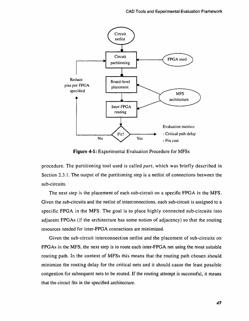
CAD Tools and Experirnental Evaluation Framework
Circuit netlist
Circuit partitioning
' I
Red ucc Board-lcvel pins per FPGA placement
spec i ficd
T In ter- FPG A routing
L 1
Evdua~ion mctrics:
Fit? - Critical path dcliiy Ycs - Pin cost
Figure 4-1: Experimental Evaluation Procedure for MFSs
procedure. The partitioning tool used is called part, which was briefly described in
Section 2.3.1. The output of the partitioning step is a netlist of connections between the
sub-circui ts.
The next step is the placement of each sub-circuit on a specific FPGA i n the MFS.
Given the sub-circuits and the netlist of interconnections, each sub-circuit is assigned to a
specific FPGA in the MFS. The goal is to place highly connected sub-circuits into
adjacent FPGAs ( i f the architecture has some notion of adjacency) so that the routing
resources needed for inter-FPGA connections are rninimized.
Given the sub-circuit interconnection netlist and the placement of sub-circuits on
FPGAs in the MFS, the next step is to route each inter-FPGA net using the most suitable
routing path. In the context of MFSs this means that the routing path chosen should
minimize the routing delay for the critical nets and it should cause the least possible
congestion for subsequent nets to be routed. If the routing attempt is successful, it means
that the circuit fits in the specified architecture.

CAO Tools and Experimental Evaluation Framework
If the routing attempt fails, the partitioning step is repeated after reducing the number
of I/0 pins per FPGA specified to the partitioner. This usually increases the number of
FPGAs needed, and helps routability by decreasing the demand from each FPGA, and
providing more "route-through" pins in the FPGAs, which facilitates routing. For
example, consider a benchmark circuit consisting of 4374 LUTs, 1728 flip flops, and 357
I/O signals, mapped to a 8-way mesh. The first mapping attempt partitioned the circuit
into 8 sub-circuits, and therefore 8 separate FPGAs. The sub-circuits were placed on a 2 X
4 mesh of FPGAs and then inter-FPGA routing was performed. Only 60% of the
inter-FPGA nets were successfully routed. The mapping procedure was repeated by
reducing the number of pins per FPGA specified to the partitioner, untii 100% of the
inter-FPGA nets were routed. The circuit was routable on a 3 X 4 array and the number of
FPGA U 0 pins specified for the partitioner was 100 (out of a possible 192).
For some circuits the routing attempt may fail even after increasing the array size. For
such cases, the mapping attempt is abandoned when the logic utilization becomes very
low after partitioning (15% or less).
The inter-FPGA routing problem is unique for each architecture and this requires an
architecture-specific router. We developed a generic router that cm be used for different
architectures, but it did not give satisfactory resulis. Eüch architecture has unique features
thai can be exploited by the routing tool to give superior results. Therefore we developed
an architecture-specific router for each class of architectures that we explored.
4.1.1 Assumptions
In an aciual MFS, the inter-FPGA routing step is followed by pin assignment,
placement and routing within individual FPGAs. Performing these tasks will provide us
with accurate routing delays within each FPGA, but will require an exorbitant amount of
time and effort. We believe that a better alternative is to perform static timing analysis
after inter-FPGA routing, assuming constant routing delay within each FPGA, to obtain a
sufficiently accurate estimate of the MFS speed. We assume that after inter-FPGA routing,
the pin assignment, placement, and routing step for each FPGA will succeed for the
reasons outlined below.

CAD Tools and Experirnental Evaluation Framework
FPGA Pin Assignment
Recall from Section 2.3.4 that the pin assignment step chooses specific wires and
FPGA pins for each connection given by the inter-FPGA router. If the FPGA pin
assignment is done randomly, it is likely to lock pins in places that make intra-FPGA
placement and routing more difficult, and may cause routability and speed problems for
the FPGA.
We conducted an experimental study to investigate the effects of pin locking on the
routability and speed of FPGAs [Kha195]. Sixteen benchmark circuits were placed and
routed on FPGAs with and without a variety of pin constraints. The FPGAs used were the
Xilinx XC4000 family of FPGAs using the XACT 5.1 .O tool set as well as the Altera
FLEX 8000 family of FPGAs using the MAX+PLUS II 5.0 tool set. The experimental
results show that the average increase in the critical path delay due to random pin
assignment is only 5% for XC4000 FPGAs and only 3.6% for the FLEX 8000 FPGAs
(compared to the no pin constraints case). There were no routing failures for the XC4000
FPGAs, but there were three routing failures (out of 14 circuits) for the FLEX 8000
FPGAs. Since we use the Xilinx 4013E-1 FPGA in our experiments, the results support
our assumption that pin locking will not significantly impact placement and routing results
for each FPGA in the MFS.
A detailed account of the experimental study is available in [Kha195], an expanded
version of which is given in Appendix A.
Intra-FPGA Placement and Routing After the inter-FPGA routing and FPGA pin assignment, we assume that each
sub-circuit can be successfully placed and routed on an FPGA. This is because our
experience [Kha195] and that of other researchers [Kuzn93] shows that the placement and
routing of a circuit on an FPGA will usually succeed if the FPGA logic utilization is
restricted to less than 70%. Therefore, during multi-FPGA partitioning, we restrict the size
of each sub-circuit to at most 70% of the FPGA logic capacity. This almost guarantees that
the placement and routing of each sub-circuit on an FPGA will be successful.

GAD Tools and Experimental Evaluation Framework
4.2 Evaluation Metrics
To compare different routing architectures we implement benchmark circuits on each
and contrast the pin cost and post-routing critical path delay, as described below.
4.2.1 Pin Cost
The cost of an MFS is likely a direct function of the number of FPGAs and FPIDs: If
the routing architecture is inefficient, it will require more FPGAs and FPIDs to implement
the same amount of logic as a more efficient MFS. While it is difficult to calculate the
price of specific FPIDs and FPGAs, we assume that the total cost is proportional to the
total number of pins on al1 of these devices. Since the exact number of FPGAs and FPIDs
varies for each circuit implementation (in our experimental procedure, we allow the MFS
to grow until routing is successful), we calculate, for each architecture, the total number of
pins required to implement each circuit. We refer to this as the pin cos! metric for the
architecture.
4.2.2 Post-Routing Critical Path Delay
The speed of an MFS, for a given circuit, is determined by the critical path delay
obtained after a circuit has been placed and routed at the inter-chip level. We cal1 this the
post-roictirig critical pciih delny. We have developed an MFS static timing analysis tool
(MTA) for calculating the post routing critical path delay for a given circuit and MFS
architecture, which is described later in Section 4.4.3 of this chapter.
4.3 Benchmark Circuits
A total of fifteen large benchmark circuits were used in our experimental work. An
extensive effort was expended to collect this suite of large benchmark circuits. The details
of each benchmark circuit are shown in Table 4-1, which provides the circuit narne, size
(in 4-LUTs, D flip flops, and I/0 count), rough description of the functionality, the source
of the circuit and the manner in which it was synthesized. Four circuits were obtained
from MCNC [Yang9 11, two from FPGA synthesis benchmarks [Prep96], and the
remaining nine were developed at the University of Toronto (Uoff). The circuits from
MCNC were available in the XNF [Xili97] gaie-level netlist format required by Our front

CAD Tools and Experimental Evaluation Framework
end tools. AlI the circuits from [Prep96] and UofT were originally available as VHDL or
Verilog HDL models and were synthesized into XNF netlists using the Exemplar
[Exem94] and Synopsys Behavioral Compiler [Knap96] andlor Design Compiler
[Syno97] synthesis tools. We show these details of the benchmark circuits because we feel
that the MCNC circuits that have been used so far in MFS architecture studies rire
insufficient in tems of size and variety to 'stress' different architectures and the mapping
tools used. Speci fically, we found that they are easier to partition and map compared to the
other real circuits that we use in this work.
Circuit 7 Size Function Source, Synthesis tool used (if
applicable) --
4374 LUTs, 7 1 7 2 8 ; F s . 357 110 signals
Sequential circuit MCNC
s384 17 6097 LUTs, 1463 FFs, 134 I/O signals
~38584
spla
Sequential circuit
2900 LUTs Scalcd down version 440 FFs, 260 1/O signals of MIPS R4000
cspla
MCNC
4396 LUTs 145 1 FFs, 292 I/O signals
- - - -
PREP, VcriIog modcl synthc- sizcd using Exemplar
gra
Scquential circuit
3423 LUTs O FFs, 62 V 0 signals
2039 LUTs O FFs, 62 VO signals
2560 LUTs 64 FFs, 133 UO signals
MCNC
1540 LUTs 200 FFs, 20 VO signals
Combinational Cir- cuit
Clone of spla
5366 L ü ï s 1040 FFs, 60 VO signals
MCNC
UoiT, Generclted using GEN[Hutt96]
- -
2494 LUTs 1 156 FFs, 144 V 0 signals
64-bit multiply-accumulate
ckt.
Uofï, Vcrilog modcl synthc- sizcd using Synopsys
8-bit HW sort engine UofT, Verilog model synthe- sized using Synopsys
16-bit, 8-stage FIR filter
fpsdes
Uoff, Verilog mode1 synthe- sized using Synopsys
Graphics accelcra- tion
circuit
spsdes
Uofï, circuit gencrated using tmcc[Gall95]
3484 LUTs 1008 FFs, 69 U 0 signals
3452 LUTs 982 FFs, 69 VO signals
Fastest pseudo DES circuit
Table 4-1: Benchmark Circuits
Uofl, Verilog model synthe- sized using Synopsys
Smaliest pseudo DES circuit
UofT, Verilog model synrhe- sizcd using Synopsys

CAD Tools and Experimental Evaluation Framework
Circuit I l Size
- -
3617 LUTs UofT, VHDL mode1 synthesized 58 10 FFs, 84 W 0 signals usine Exemplar
Function
set
Source, Synthesis tool used (if applicable)
ralu32 584 FFs, 98 If0 signals
Table 4-1: Benchmark Circuits
2553 LUTs
i ir l6
4.4 CAD Tools
ALU, and control Iogic
The CAD tools developed for mapping circuits to architectures are described in this
section. Our main goals in creating these CAD tools were:
32-bit register file, sized using Synopsys
3 149 LUTs 532 FFs, 52 VO signals
1. To create a tool suite that was flexible enough to map circuits to a wide range of MFS routing architectures.
PREP, VHDL modcl syntlie-
2. To employ a suitable algorithm for each task to obtain results that were as good as the results reported elsewhere or at least not significantly worse.
16-bit IIR filter
3. To minimize the development time of the CAD tools to allow sufficient time for MFS routing architecture exploration, which is the main focus of this research. We wanted io avoid spending an excessive arnount of time on CAD tool optimization.
UoU, VHDL modcl synthesizcd using Synopsys
4.4.1 Multi-way Partitioning
Recall from Section 2.3.1 that multi-way partitioning can be done using either a direct
approach or by recursive bipartitioning. The problem with direct multi-way partitioning is
that it has no information about the MFS architecture and hence routability constraints
between different sub-circuits. Ideally, it is best to use an architecture-driven multi-way
partitioner. Since we did not have access to such a partitioner, we implemented multi-way
partitioning by recursive bipartitioning which is followed by board-level FPGA
placement. The motivation behind this approach is to provide enough locality in
post-partitioning and placement netlists for architectures like the mesh and HTP that have
local inter-FPGA connections. The partitioning tool used in the recursive bipartitioning
procedure is called part [Ga1194], which was briefly described in Section 2.3.1.

CAO Tools and Experirnental Evaluation Framework
RBTO / * Recursive Bipartitioning Tool * /
Inputs : C: circuit to be partitioned; FPGA logic and pin capacity;
Outputs : K sub-circuits, each of which fits into a single FPGA;
Variables : cur-ckt: current sub-circuit to be bipartitioned; partl, p a r t 2 : sub-circuits obtained after bipartitioning;
( / * begin RBT * / cur-ckt = C; bipart(cur-ckt); / * sub-circuit c (0.55 * cur-ckt) * / push partl on to stack; push part2 on to stack; while (stack is NOT empty) { pop top of stack into cur-ckt; if(cur-ckt fits into FPGA) / * logic u t i l . c= 70% * /
assign a partition number to cur-ckt and store it; else
bipart(cur-ckt); / * sub-circuit < (0.55 * cur-ckt) * / push partl on to stack; push part2 on to stack;
1 1
} / * end RBT * /
Figure 4-2: Pseudo-code for RBT
We developed a tool for multi-way partitioning, called the Recursive Bipartitioning
Tool (RBT), which partitions a given circuit into the minimum possible number of
FPGAs, given the FPGA logic and pin capacity. The pseudo-code for RBT is shown in
Figure 4-2. First the circuit, denoted by C, is bipartitioned into two sub-circuits, pan1 and
part2 such that the number of wires between the sub-circuits is minimized. Also each
sub-circuit is restricted to be between 45% and 55% of the size of cw-ckt to keep the
partitions balanced. The two sub-circuits are then pushed on to a stack. Next, the while
loop shown in Figure 4-2 is executed until the stack is empty. In the while loop, the
sub-circuit on the top of stack is examined first to check if it fits in the FPGA used. To
ensure intra-FPGA routability (as discussed in Section 4.1. l), only sub-circuits whose size

CAD Tools and Experimental Evaluation Framework
Figure 4-3: The Partitioning Tree for the Circuit spsdes Generated by RBT
is at most 70% of FPGA logic capricity are chosen as feasible partitions. If the sub-circuit
does not fit into the FPGA, it is bipartitioned and the resulting partitions are pushed on the
top of stack. When the while loop terminates, al1 the partitions obtained by RBT are
available. The RBT generates the partitioning tree for a circuit in a sequence illustrated in
Figure 4-3 for the benchmark circuit spscies. The circuit is represented by the root node (O)
in the tree and the leaf nodes (shaded circles) represent the final partitions. The node
number indicates the sequence in which the nodes are generated during recursive
bipartitioning. Thus nodes 1 and 2 are genetated drst from node 0, and nodes 13 and 14
are generated last from the node 1 1.
A multi-way partitioning tool can be evaluated using two metrics: first, it should
minimize the total number of FPGAs required in the partitioned circuit and second, it
should minimize the total cut size. Unfortunately, none of the published work on
multi-way partitioning [Kuzn94, Chan95, Chou95, Roy95, Kim961 used the Xilinx 4013
FPGA. Therefore we cannot compare RBT to the other multi-way partitioners that have
been previously developed. The partitioning tool used in RBT (part) is based on the
widely used FM algorithm and i t is reasonable to expect that its results are not
significantly worst compared to other multi-way partitioning tools reported in the
literature [Kuzn94, Chan95, Chou95, Roy95, Kim96-j.

CAD Tools and Experirnental Evaluation Frarnework
Figure 4-4: Semi-perimeter of the Net Bounding Box
4.4.2 Placement
Following multi-way partitioning of the circuit, the placement tool assigns each
sub-circuit to a specific FPGA in the MFS. If the MFS architecture h a s no local
connections, as in partial crossbar and HCGP, any arbitrary placement is acceptable. This
is because in such architectures any pair of FPGAs is uniformly connected. For
architectures that have local connections, such as the Mesh, HTP, and HWCP, a placement
algorithm is required to place highly connected sub-circuits into adjacent FPGAs, to
mini mize the inter-FPGA routing resources needed.
Placement for Mesh Architectures
For placement on the mesh architectures such as the 8-way torus and HTP, we
developed a tool called the Mesh Placement Tool (MPT) that uses a version of
force-directed placement algorithm presented in [Shah9 11. That algorithm was described
in Section 2.3.2 and the pseudo-code for the algorithm was presented in Figure 2- 10. To
implement the algorithm, suitable decisions on the following issues were required:
1. For calculating the cost of a given placement configuration, a rnethod of estimating the routing cost of each net is needed. The routing cost of an inter-FPGA net on a mesh is estimated by the semi-perimeter of the net bounding box. This is a commonly used method of estimating the routing cost in placement tools [Sarr96]. The number of FPGA pins required for routing a net is directly proportional to the length of semi-perîmeter of the net bounding box. For example, consider a net that connects FPGA O and FPGA 8 in Figure 4-4. Assuming that the FTGAs are placed
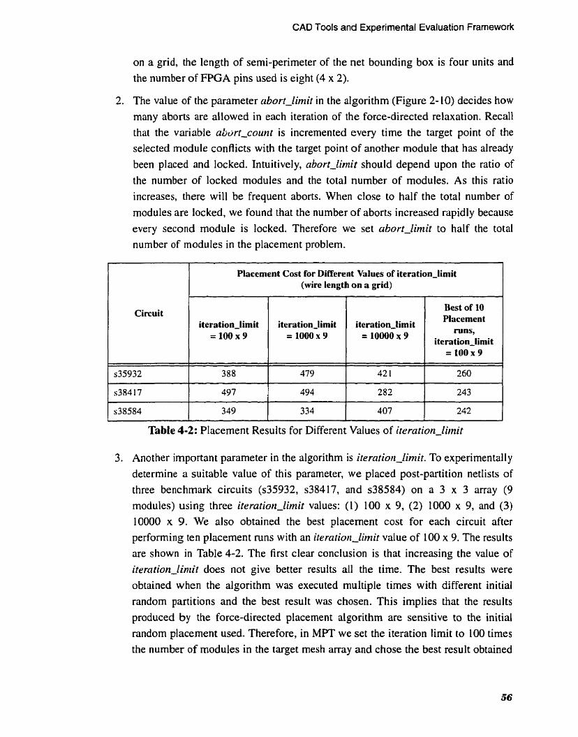
CAD Tools and Experimental Evaluation Framework
on a grid, the length of semi-perimeter of the net bounding box is four units and the number of FPGA pins used is eight (4 x 2).
2. The value of the parameter abo-lirnit in the algori thm (Figure 2- 10) decides how many aborts are allowed in each iteration of the force-directed relaxation. Recall that the variable aliürt-count is incremented every time the target point of the selected module conflicts with the target point of another module that has already been placed and locked. Intuitively, abortJimit should depend upon the ratio of the nurnber of locked modules and the total number of modules. As this ratio increases, there will be frequent aborts. When close to half the total number of modules are locked, we found that the number of aborts increased rapidly because every second module is locked. Therefore we set abort-limit to half the total nurnber of modules in the placement problem.
Placement Cost for Different Values of iteration-limit (wire length on a grid)
Table 4-2: Placement Results for Different Values of iteration-limit
Circuit
3. Another important parameter in the algorithm is ireration-limit. To experimentall y determine a suitable value of this parameter, we placed post-partition netlists of three benchmark circuits (~35932, ~38417, and ~38584) on a 3 x 3 array (9 modules) using three iteration-lirnif values: (1) 100 x 9, (2) 1000 x 9, and (3) 10000 x 9. We also obtained the best placement cost for each circuit after perforrning ten placement runs with an iteratiori-limit value of 100 x 9. The results are shown in Table 4-2. The first clear conclusion is that increasing the value of ireration-liniit does not give better results al1 the time. The best results were obtained when the algorithm was executed multiple times with different initial random partitions and the best result was chosen. This implies that the results produced by the force-directed placement algorithm are sensitive to the initial random placement used. Therefore, in MPT we set the iteration limit to 100 times the number of modules in the target mesh array and chose the best result obtained
iteration-limit =1ûûx9
iteration-limit = 1000 x Y
iteration-limit = 'Ooo0
Best of 10 Placement
mns, i t en t io~ l imi t
= l O O x 9

CAO Tools and Experimental Evaluation Framework
out of ten placement runs. We used only three benchmark circuits in this experiment because the other benchmark circuits were not available when we were developing MPT.
To evaluate the quality of MPT, we did not have any published results for cornparison.
We looked at the reduction in placement cost obtained compared to the cost of the initial
random placement. Across al1 circuits, the reduction in placement costs ranged from 39%
to 61 %. It is difficult to calculate an average reduction in the placement cost because
placements were done for many array sizes for each circuit (in an attempt to make the
circuits route on the mesh architecture).
Placement for the HWCP Architecture
Recall from Section 3.4.3 that the HWCP architecture consists of clusters of FPG.4s
with hardwired connections between üI1 the FPGAs in each cluster. The placement
problem for the HWCP architecture is an üssignment problem. Each cluster of sub-circuits
in the partitioning tree of a circuit needs to be assigned to a specific cluster of FPGAs in
the target HWCP architecture. The goal is to assign closely connected clusters of
sub-circuits to adjacent FPGA clusters in the architecture to rninimize the inter-FPGA
routing cost.
The cluster size depends upon the value of the Cs parameter in the target HWCP
architecture. Recall from Section 3.4.3 that Cs represents the number of FPGAs within
each hardwired cluster in the HWCP architecture. For example, consider the partitioning
tree of the ~35932 circuit shown in Figure 4-5(a). The final partitions or sub-circuits are
represented by shaded circles. Assume that this circuit is to be mapped to an HWCP
architecture that consists of nine FPGAs with a cluster size of three (Cs = 3). The approach
used for clustering of sub-circuits is shown in Figure 4-5(a), where adjacent sub-circuits
are grouped into each cluster, represented by dashed lines covering the sub-circuits. We
start from the leftmost sub-circuit in the partitioning tree which is grouped with the next
two sub-circuits to the right. An ideal approach for generating the partitioning tree would
be as shown i n Figure 4-S(b), where the partitioning tree matches the target HWCP
architecture topology. Developing suc h an archi tecture-driven partitioning tool is very

CAD Tools and Experimental Evaluation Framework
Figure 4-5: Partitioning and Placement of the ~35932 circuit on the HWCP Architecture: (a) Actual (b) Ideal
time consurning, therefore we used the partitioning tree generated by our recursive
bipartitioning tool (RBT). While our approach towards partitioning and placement for
HWCP is sub-optimal, we expect that the mapping results would still give valuable insight
into the routability and speed performance of the HWCP architecture.
4.4.3 MFS Static Timing Analyzer
In synchronous digital circuits, the maximum possible speed is determined by the
slowest combinational path in the circuit implementation, which is called the critical path.
Static timing analysis tools are used to identify the critical paths in designs irnplemented at
the chip-level [Joup87] as well as the board-level jChan97J. Timing analysis is also used
in timing-driven hyout tools, to estirnate the slack of each connection in the circuit. The

CAD Tools and Experimental Evaluation Framework
slack of a connection is defined as the delay that can be added to the connection without
increasing the critical path delay. Connections with low slack values are routed using fast
paths to avoid slowing down the circuit.
For a given circuit, the speed of an MFS is determined by the critical path delay
obtained after a circuit has been placed and routed at the inter-chip level. We developed an
MFS siatic timing analysis tool (MTA) for calculating the post-routing critical path delay
for a given circuit and MFS architecture. The operation and modeling used in the MTA are
described in this section.
The delay values used by the MTA are given in Table 4-3. These values were obtained
from the Xilinx [Xili97] and Kube [ICub97] data sheets and some design experience.
1 FPGA input pnd delay 1 1.4 1
Item
Intrn-FPGA CLB-to-CLB routing dclay
-
Delay (ns)
2.5
- - - - 1 FPID crossing dclay (including pad delays) 1 0 1
FPGA output pnd dclay
CLB dclay (without using H-LUT)
CLB dclay (via H-LUT)
1 PCB incc delay I 3 I
3.2
1.3
2.2
I - - 1 FPGA route through delay 1 ° 1
Table 4-3: The Delay Values Used in the Timing Analyzer Model
Since we do not perform individual FPGA placement and routing, we approximate the
CLB-to-CLB delay as a constant. The value of 2.5 ns for CLB-to-CLB routing delay is
roughly half the delay on a long line for XC4013E-1 FPGA, which is a pessimistic
estimate. Although using a single delay value is somewhat inaccurate, it still gives us a
good estimate of the post-routing critical path delay of an MFS because it is dominated by
off-chip delay values.
The configurable logic block (CLB) in the Xilinx 4000 family of FPGAs [Xili97]
consists of two 4-LUTs, called F and G, whose outputs feed into a 3-LUT called the
H-LUT. The H-LUT is not always used when implementing combinational logic functions

CAD Tools and Experimental Evaluation Framework
in the CLB (the CLB outputs corne directly from F and G LUTs). Obviously, the CLB
delay is more when the H-LUT is used because of the extra logic in the paths from CLB
inputs to the outputs as given in Table 4-3.
We now describe the operation of the MTA. First, it calculates the critical path delay of
the un-partitioned design using a widely used method called the block-oriented technique
[Joup87]. In this step it is assumed that the circuit is implemented on a hypothetical single
large FPGA that has the same logic block and interconnect delay (shown in Table 4-3) as
the FPGA used in the MFS (Xilinx 401 3). The critical path delay of the un-partitioned
design is denoted by CPD.
In the second step, MTA calculates the post-partition critical path delay, denoted by
CPD-PP. This is the critical path delay obtained by analyzing the circuit netlist after i t has
been partitioned into multiple-FPGAs. It is assumed that the FPGAs are interconnected on
a custom PCB and the circuit is annotated with the inter-chip delays from which CPD-PP
is calculated. The inter-chip delay for connecting a CLB in one FPGA to a CLB in another
FPGA is given by the sum of the following delay values (given in Table 4-3): CLB to
output pad routing delay (assumed to be equal to the CLB-to-CLB routing delay), PCB
trace delay and input pad to CLB routing delay (assumed to be equal to the CLB-to-CLB
routing delay). CPD-PP provides a lower bound on the post-routing critical path delay
(denoted by CPD-PR) that is obtained using general purpose MFS. This is because for any
circuit, CPD-PR can be no better CPD-PP due of the delays introduced by board-level
programmable routing in general purpose MFSs.
Lastly, the MTA reads the MFS architecture description and the routing path for each
inter-FPGA net, as provided by the inter-FPGA router. From this information, the circuit
is annotated with the inter-FPGA delays for the given MFS, from which the post-routing
critical path delay (CPD-PR) is calculated. After inter-FPGA routing, a path connecting
two FPGAs may traverse other FPGAs and FPIDs. In such cases the FPGA and FPID
crossing delays and the input and output pad delays, shown in Table 4-3, are used for
calculating the routing delay.

CAD Tools and Experimental Evaluation Framework
Sample Results Obtained Using the MTA The capabilities of the MTA are demonstrated by the speed estimates obtained for al1
the benchmark circuits at three levels of circuit implementation: pre-partitioning (single
hypothetical FPGA), post-partitioning (custom MFS), and post-routing (actual MFS).
Table 4-4 shows the critical path delays obtained by using MTA for al1 the benchmark
circuits mapped to the partial crossbar architecture. Column 1 shows the circuit name and
column 2 shows the number of FPGAs required to implement the circuit on the partial
crossbar. Columns 3 and 4 show the normalized pre-partitioning (CPD) and
post-partitioning (CPD-PP) critical path delays respectively. The delay values in each row
are normalized to the pre-partitioning critical path delay value (CPD). Column 5 shows
the normalized post-routing critical path delay (CPD-PR).
Circuit I Normalized critical path delay I
Pre-partitioning, Post-partitioning, Post-routing, CPD CPD-PP CPD-PR
8 1 .O 1 .O9 1.68
~38584
mi ps64
spla
cspla
mac64
Table 44: Critical Path Delays at Different Levels of Circuit Implementation
fpsdes
spsdes
ochip64
d u 3 2
iirl6
1 sort8 1 12 1 1 .O I 2.10 1 3.68 1
9
14
18
18
6
1 Average 1 10 1 1.0 I 1.49 I 2.66 I
9
8
8
9
6
I .O
1 .O
1 .O
1 .O
1 .O
1 .O
1 .O
1 .O
1 .O
1 .O
1.32
1-37
2.26
2.28
1.47
-
1.96
2.0 1
5.16
5.36
2.40
1-42
1.25
1.32
1-71
1 .O5
2.36
1 .80
2.86
3.45
1.24

CAD Tools and Experimental Evaluation Framework
Compared to single FPGA implementation, Table 4-4 illustrates the delay penalties
incurred due to partitioning and programmable routing at the board level. The CPD-PP
value across al1 the circuits is on average 49% more than the CPD value, and in some cases
is more than a factor of 2 greater. Similarly, the average CPD-PR value across al1 the
circuits is a factor of 2.5 times more than CPD and up to 5 times more. Table B-1 in
Appendix B is similar to Table 4-4 except that it shows the actual (un-normalized) critical
path delay values.
Note that our definition of the critical path (obtained using the block-oriented
technique) suffers from two limitations: First, we cannot guarantee that the critical path is
not a false püth. Second, in some circuits that irnplernent multi-cycle operations, the
critical path in each cycle may be different from what we define as a critical path. Despite
these limitations, the block-oriented technique gives reasonably accurate results and is
widely used in practice.
4.4.4 Inter-FPGA Routing Algorithms
The routing algorithms developed for the various MFS architectures explored in this
research are described in this section. Initially, we developed a generic MFS router that
uses a topology independent routing algorithm. As we mapped circuits to different
architectures, we found that the generic router had major problems with different aspects
of each architecture. Therefore we developed architecture-specific routers to obtain the
best possible routing results for each architecture.
The two goals of an inter-FPGA router are achieving routing completion and obtaining
the best possible speed performance. For hybrid architectures that use a mix of fast
hardwired connections and slow programmable connections, timing-driven routing shouid
be used to obtain the best possible speed performance.
A Topology-Independent Router
We developed a topology independent inter-FPGA routing tool called FPSROUTE. It
represents the MFS architecture using an undirected routing graph whose nodes are
FPGAs and FPIDs. Each edge between any pair of nodes is assigned a weight that is equal
to the number of wires between those two nodes. For exarnple, consider the Cway toms

CAD Tools and Experimental Evaluation Framework
I I
1 1 i
Figure 4-6: (a) Cway Toms architecture (b) Its Routing Graph
architecture and its routing graph illustrated in Figure 4-6. Each edge in Figure 4-6
represents 47 wires, hence the weight of each edge in the routing graph is also 47.
Given the routing graph for any MFS architecture and the netlist of connections
between FPGAs, the well known maze routing algorithm [Lee611 is used to find the
shortest available path for routing each net. After each net is routed, the edge weights in
the routing paths are updated to reflect the reduction in available wires. The maze routing
algorithrn is suitable for routing two-terminal nets and cannot be used directly for routing
multi-terminai nets. One approach for routing multi-terminal nets is to decompose each
such net into a set of two terminal nets and route the two-terminal nets independently. But
this approach leads to inefficiencies as discussed in Section 2.3.3. FPSROUTE uses an
algorithm called the single component growth algorithm [Kuh86] for routing
multi-terminal nets. This algorithm starts with the net source and finds the shonest path to
the closest sink using the maze routing algorithm. Next, al1 the nodes in the routing path
are treated as possible sources and the shortest path to the next closest sink is found. This
procedure is repeated until paths to al1 the net sinks are found.
If any nets remain unrouted after the first routing attempt, repeated iterations of the
router are performed. In each iteration, al1 nets are ripped up and rerouted. The nets that
failed in the immediately previous iteration are routed first, followed by nets that failed in
the next previous iteration, and so on. Thus in each iteration, the 'history' of failed nets is
3
1 1 1
I I
FPGk 2
C FPGA O
C
FPGA 1
I I I
FPGA 3
C
FPGA 4
FPGA 7
FPGA 6
, , FPGA 5
_>
FPGA 8 3

CAD Tools and Experimental Evaluation Frarnework
considered when ordering the nets for routing. To sumrnarize, FPSROUTE uses the
traditional rnulti-pass maze routing approach, with a 'move-to-front' heuristic, for
topology-independent inter-FPGA routing.
Due to its generic nature. FPSROUTE gives inferior routability and speed results for
different MFS architectures. It is compared to the other architecture-specific routers in
subsequent sections. Note that this basic maze routing approach is used i n the other
architecture-specific routers to handle the last few 'difficult-to-route' nets that are
encountered in some circuits.
Routing Algorithm for Mesh Architectures
The problem with FPSROUTE is that it concentrates exclusively on finding the
shortest path for each net while ignoring issues like routing congestion.
The routing problem in the mesh architectures is complicated by the fact that the
FPGAs are used for both logic and routing. After a circuit is rnapped to a mesh
architecture, each FPGA will have a number of I/O pins unused after al1 the pins needed
for sources and sinks in that FPGA are accounted for, called free pins. An FPGA should
have at least two free pins if i t is to permit a route to pass through it.
Consider a net that connects the nodes O and 4 in Figure 4-6(a). The shortest paths for
routing the net are (O 1 4) and (O 3 4). The final choice of the routing path depends upon
two things: first whether enough free pins are available in the intermediate FPGAs used in
each path (1 and 3), and second whether routing congestion is rninimized or not. The path
that has the largest nurnber of wires available will minimize congestion for the subsequent
nets to be routed.
We developed a mesh routing tool called MROUTE that uses a heuristic tuned to the
routing requirements of the mesh architecture. It first routes al1 those nets that do not use
any free pins (e.g. nets connecting adjacent FPGAs). It then routes al1 two-terminal nets
using an algorithm that enurnerates al1 possible shortest paths between source and target.
A shortest path is chosen that attempts to minimize the congestion for the subsequent nets
to be routed and utilizes intermediate FPGAs that have the most number of free pins.
Since the typical array is small (at most 6 X 8 in our case), enumeration of al1 possible

CAD Tools and Experirnental Evaluation Framework
shortest paths is computationally feasible. For multi-teminal nets, a modified form of the
sing!e component growth algorithm, described in the previous section, is used. The
algorithm is adapted for mesh architectures to consider free pins when routing
multi-terminal nets. Specifically in the multi-terminal net routing algorithm, during the
breadth-first-search (BFS) to find a net sink, the FPGAs that do not have free pins are not
marked as possible intermediate FPGAs in a routing path. If the first routing attempt fails,
it uses a rip-up and reroute approach similar to that used in FPSROUTE.
Circuit
mi ps64
spln
cspla
111x64
sort8
tir16
fpsdcs
spsdes
rniu32
iirl6
Table 4-5: Cornparison of FPSROUTE and MROUTE
Average
MROUTE gave consistently better results compared to the topology-independent
router FPSROUTE as illustrated in Table 4-5. Across ten circuits mapped to several array
sizes, the percentage of nets routed by MROUTE increased by 4% on average and up to
7% more in the best case, compared to FPSROUTE.
#FPGAs
14 (2 x 7)
18 (3 x 6)
18 (3 x 6)
6 (2 x 3)
12 (3 x 4)
10 (2 x 5)
9 (3 x 3)
8 (2 x 4)
9 (3 x 3)
6 (2 x 3)
Routing Algorithm for Partial Crossbar
Recall from Section 2.3.3 that the inter-FPGA routing problem in the partial crossbar
involves choosing a specific FPlD for routing each net such that al1 nets route. The router
1 O
% nets routed in the 8-way mesh
FPSROUTE
9 1
8 3
8 1
7 3
7 8
92
84
8 1
80
8 9
83
MROUTE
92
90
85
77
80
96
88
84
87
89
87

CAD Tools and Experirnental Evaluation Framework
PCROUTE-ALGORITHM C route al1 nets that contain an FPID as a net terminal; route al1 nets using bestqath0 in decreasing order of fanout; if(any net rernains unrouted)
Iterate N times using a 'move-to-front' strategy for failed nets ;
if(any net remains unrouted) report routing failure;
else report routing success;
1
bestsath ( ) ( calculate the routing cost for the net through al1 available FPIDs; choose the least cost routing path (through a specific FPID) if(routing attempt using a single FPID fails) use maze routing to route the net;
if(maze routing atternpt fails) report routing failure for the net;
1
Figure 4-7: Pseudo-code for the Routing Algorithm used in PCROUTE
should minimize the number of hops used in each source to sink path in each net in order
to obtain good speed performance.
We developed a routing tool, called PCROUTE, that uses a heuristic algorithm tuned
to the requirements of the partial crossbar architecture. which is illustrated in Figure 4-7.
Recall from Section 3.3 that in the partial crossbar, the circuit UO signals are connected to
the FPGAs through FPIDs. Such connections (nets) have one FPGA and one FPID as the
net terminais. The algorithm routes such nets first because there is no flexibility in routing
such nets. Next al1 the nets are routed in decreasing order of fanout, the highest fanout net
first and two-terminal nets last. The reason behind this is that as the wires between the
FPGAs and FPIDs get used up in routing, it becomes increasingly difficult to route high
fanout nets. This is because an FPID with wires available for connecting to al1 the FPGAs
belonging to the net may not be available. Therefore it is better to route such nets first. If
the routing attempt fails a rip up and reroute strategy is used, which is similar to the one
employed in FPSROUTE.

CAD Tools and Experimental Evaluation Framework
For each net, the bestgarh() routine evaluates potential routing paths through al1
available FPIDs. The cost function used to choose an FPID attempts to guarantee balanced
usage of FPIDs and preserve the most options for two-hop routing of subsequent nets to be
routed. It is as follows: consider a partial crossbar that consists of X FPGAs and Y FPIDs.
Consider an N-terminal net called M. Let F denote the set of FPGAs belonging to M, Le. F
Let Aik denote the number of available wires between FPGA i and FPID k. The cost of
routing the net M through FPID k, C(M, k), is given by:
Recall from Section 3.3 that P, is the number of pins per subset. An FPID that has the
lowest routing cost for the net M is chosen for routing that net. If the routing attempt using
a single FPID fails, the net is processed by a maze router. The routing path obtained by the
maze router i n such cases will involve the usage of multiple intermediate FPGAs and
FPIDs as illustrated in Figure 4-8. Consider a net whose source lies in FPGA 1 and sinks
lie in FPGAs 2 and 4. A single FPID cannot be used for routing the net because the
required connections between FPGAs and FPIDs are used up by other nets. Hence the
routing path specified by dashed lines in Figure 4-8 will be chosen by the maze router. The
path between FPGA 1 and FPGA 4 will require 4 hops: FPGAl to FPID AI FPID A to
FPGA 2, FPGA 2 to FPD B, and FPID B to FPGA 4.
PCROUTE gives excellent routability and speed results for al1 the benchmark circuits,
which were routed without requiring any iterations. The routing problem for the partial
crossbar becomes more difticult as the value of P, is reduced. This is because of reduced
routing flexibility due to the low pin count FPIDs used in such cases. Irrespective of the
value of Pt, PCROUTE achieves 100% routing completion and produces two-hop routing
for al1 the nets in alrnost al1 circuits. For only two circuits, for the specific case of P, = 4, it
produced multi-hop routing paths for a negligible number of nets (1 out of 991 nets for the
first circuit and 3 out of 645 nets for the second). In practical terms, this means it gives
almost optimal results for al1 of our benchmark circuits because the best that a partial

CAD Tools and Experimental Evaluation Framework
Figure 4-8: Multi-hop Routing in Partial Crossbar
crossbar router can achieve is routing of every net using only two Iiops in the source-sink
path. Although we did not compare PCROUTE to the other partial crossbar routers, we
expect it to be equivalent in quality to other partial crossbar routers that have been
proposed to date [Kim961 [Mak95a] [Lin971 [Slim94]. This is because PCROUTE
performs so well across a variety of benchmark circuits, including some difficult-to-route
circuits such as spln and cspla. PCROUTE should be better than [MakgSb] for speed
because that algorithm splits each multi-terminal into a set of two-terminal nets and routes
them independently, leading to multiple hops and even possible routing failures.
PCROUTE also gives better speed results compared to the topology-independent
router FPSROUTE. This is because FPSROUTE greedily chooses the first avaiiable FPID
to route each net and does not balance the usage of FPIDs. The result is that many
rnulti-terminal nets cannot be routed using a single FPID and are forced to use rnulti-hop
routing paths.
The benchmark circuits were mapped to the partial crossbar architecture with Pt = 4
using both FPSROUTE and PCROUTE. For FPSROUTE, the average increase in
post-routing critical path delay (CPD-PR) across al1 circuits was 19% compared to
PCROUTE and 62% more in the worst case.
CAD Tools and Experimental Evaluation Frarnework
Routing Algorithm for Hybrid Architectures
Recall from Section 3.4 that the hybrid architectures use a mixture of hardwired and
programmable connections. The inter-FPGA routing algorithm for the hybrid
architectures is closely related to the partial crossbar routing algorithm in the sense that a
similar algorithm is employed when routing nets through FPIDs. However, the difference
here is that the router should also exploit the direct connections between FPGAs to
minimize the number of FPGA and FPID pins and the number of hops used, when routing
ench inter-FPGA net. This makes the routing algorithm for the hybrid architectures more
complicated compared to the partial crossbar.
We developed a routing tool, called HROUTE, that understands the hybrid
architectures and gives excellent routabiiity and speed results for al1 the benchmark
circuits.
The main objective of HROUTE is to route al1 nets using no more than two hops for
each source-sink path in each net. Wherever possible, it strives to use the direct hardwired
connections between FPGAs to minimize source-sink net delay when routing both
two-terminal and multi-terminal nets. The routing algorithm used in HROUTE is
described using the pseudo-code in Figure 4-9. First an attempt is made to route al1
possible two-terminal nets using the direct connections between FPGAs to minimize the
usage of pins and net delay. Next, al1 multi-terminal nets are routed through FPIDs using a
routing algorithm similar to that used in PCROUTE. The difference here is; first an
attempt is made to use hardwired connections for al1 possible source to sink connections.
Any sinks that remain unconnected are then linked to the source using a single FPID.
Finally, the remaining two terminal nets are routed using FPGAs or FPIDs. Any nets thrit
rernüin unrouted are processed by a maze router.
If any nets remain unrouted after the first iteration, a rip up and reroute strategy similar
to the one described for FPSROUTE is used. We found that net ordering is crucial for
obtaining good routability and speed results in HROUTE because it optimizes the usage of
MFS routing resources (FPGA and FPID pins).

CAD Tools and Experirnental Evaluation Frarnework
HROUTE-ALGORITHM { / * begin HROUTE * /
route al1 nets that contain an FPID as one of the net terminals; route al1 possible two-terminal nets connecting adjacent FPGAs using hardwired connections; route al1 multi-terminal nets using bestjath-multi(); for (al1 remaining two-terminal nets) { route the net using the most suitable intermediate FPGA; if(no intermediate FPGA is available)
route the net using the most suitable FPID; 1 if(any nets remain unrouted) / * Erom eaxlier atternpts * / route each net using the maze router;
if (any nets remain unrouted) iterate N times using a 'move-to-front' strategy for f a i l e d nets;
if(any nets remain unrouted) / * even after iterations * / report routing failure
) / * end HROUTE * /
bes t j a th-mu1 t i ( ) { if(enough free pins are available in the source FPGA)
connect the source to al1 possible sinks using hardwired connections;
if (any sinks remain unconnected) calculate the routing cost of connecting the source to the sinks using al1 available FPfDs; choose the least cost routing path using a single FPID;
Figure 4-9: Pseudo-code for the Routing Algorithm used in HROUTE
Timing-Driven Routing Algorithm for Hybrid Architectures
A problem with HROUTE is that i t is not timing-driven and hence does not fully
exploit the fast hardwired connections in the hybrid architectures to obtain the maximum
possible speed. To overcome this deficiency, we developed a timing-driven rouiing tool for
the hybrid architectures, called HROUTE-TD, that uses path based s tatic timing anal ysis
to identify the critical nets and route ihem using the fast hardwired connections.
The main objectives of HROUTE-TD are to try to route al1 critical nets using direct
connections and to route al1 other (non-critical) nets using no more than two hops for each
source-sink path. The algorithm used in HROUTE-TD can be best described by using the
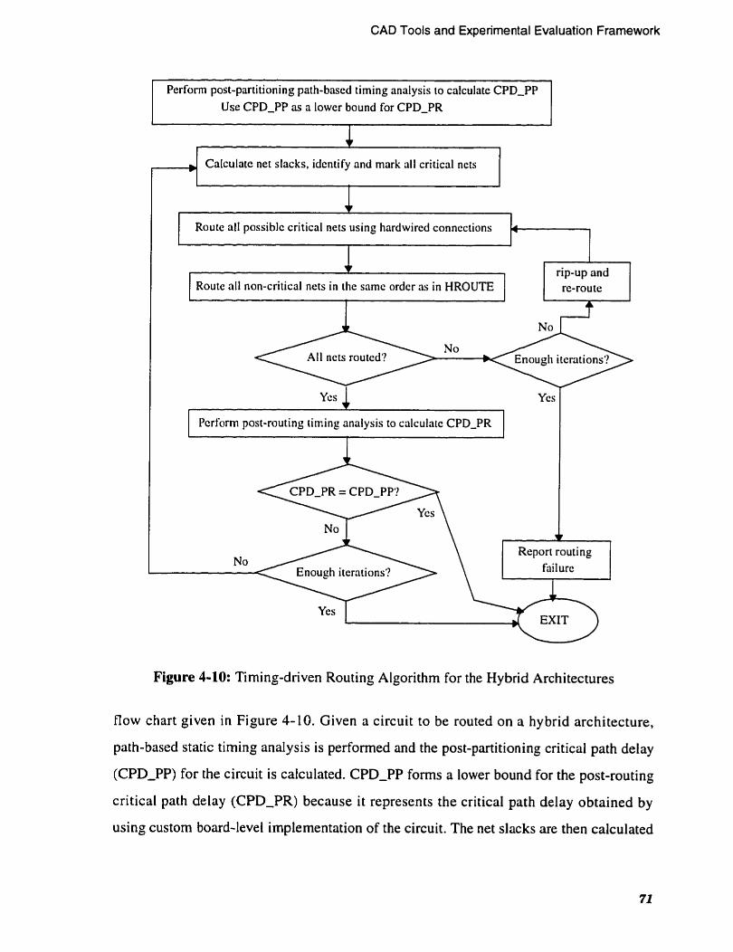
CAD Tools and Experirnental Evaluation Framework
Perforrn post-partitionhg path-based timing analysis io caiculate CPD-PP Use CPD-PP as a lowcr bound for CPD-PR
4 Calculate net slacks, idcntify and mark al1 critical nets
1 Route Û I I possible critical nets using hardwircd connections lt--1 Route al1 non-critical nets in thc sarnc ordcr as in HROUTE
I No
AI1 nets routcd?
I
1 Pcrform post-routing timing analysis to calculaie CPD-PR 1 I
Figure 4-10: Timing-driven Routing Algorithm for the Hybrid Architectures
flow chart given in Figure 4-10. Given a circuit to be routed on a hybrid architecture,
path-based static timing analysis is performed and the post-partitioning critical path delay
(CPD-PP) for the circuit is calculated. CPD-PP forms a lower bound for the post-routing
critical path delay (CPD-PR) because i t represents the critical path delay obtained by
using custom board-level implementation of the circuit. The net slacks are then calculated

CAD Tools and Experimentat Evaluation Framework
for each inter-FPGA net and the critical nets are identified and rnarked. A critical net is
defined as an inter-FPGA net whose slack is Iess than the delay incurred for connecting
two FPGAs via an FPID, which is the delay of a programmable connection.
In the next step, an attempt is made to route al1 critical nets using hardwired
connections. Among the critical nets, two-terminal nets are routed first because such nets
are the most suitable candidates for using direct hardwired connections. It is difficult to
route multi-terminal nets using only hardwired connections (without FPID) because many
free pins are required in the source FPGA, which are usually not available. This is
followed by the routing of non-critical nets in the same order as that used in HROUTE. If
any nets remain unrouted, this implies that the first iteration of timing-driven routing is
unsuccessful. In such cases, a rip-up and re-rouie similar to that employed in FPSROUTE
is used. The failed nets from the previous iterations are assigned the highest priority in the
current iteration. Once the failed nets are routed, the remaining nets are routed in the same
order as that in the very first routing pass.
Circuit I lFPGAS delay, CPD-PR
I
~35932
~38417
1 spsdes 1 8 1 1 .O5 1 1 .O
8
9
1 .O
1 .O
L
firl6
lF
Fpsdes
Table 4-6: Cornparison of HROUTE and HROUTE-TD
mips64
spla
HROUTE
1 .O8
1 .O1
10
4
9
HROUTE-TD
1 .O
1 .O
14
18
1.12
1.21
1.16
1 .O4
1.1 1
1 .O
1 .O
1 .O

CAD Tools and Experimental Evaluation Framework
Circuit #FPGAs
Table 4-6: Comparison of HROUTE and HROUTE-TD
Normalized post-routing critical path delay, CPD-PR
9
6
10
If the timing-driven routing attempt succeeds, timing analysis is performed to
calculate CPD-PR. If CPD-PR achieves its lower bound, the timing-driven routing
attempt is terminated because i t has already achieved its goal. Otherwise, net slacks are
again calculateri and iterations of timing-driven routing are performed. We found that the
iterations to improve the timing did not result in any significant reduction in the value of
CPD-PR compared to the value given by the first iteration. Even after using ten iterations,
the best case reduction in CPD-PR was only 3% across al1 benchmark circuits.
HROUTE-TD gave significant speed improvements cornpared to the
non-timing-driven router HROUTE, as illustrated in Table 4-6. The benchmark circuits
were mapped to the HCGP architecture using HROUTE and HROUTE-TD. In Table 4-6,
the first column shows the circuit name ciilci the second coizrrin shows the number of
FPGAs required to implement that circuit. Columns 3 and 4 show the normalized
post-routing critical path delay (CPD-PR) obtained using HROUTE and HROUTE-TD
respectively. For each circuit, the CPD-PR value obtained using HROUTE-TD is set as 1.
Compared to HROUTE-TD, the average increase in the critical path delay across al1
circuits was 1 O%, and up to 2 1 % more. These results demonstrate that it is essential to use
a timing-driven router in order to obtain the maximum possible speed for the hybrid
architectures. Table 8-2 in Appendix B is similar to Table 4-6 except that it shows the
actual (un-normalized) critical path delay values.
The experimental framework and the CAD tools used for mapping the benchmark
circuits to different architectures were described in this chapter. The architecture
HROUTE
1.13
1 .O0
1.10
HROUTE-TD
1 .O
1 .O
1.0

CAD Tools and Experimental Evaluation Frarnework
evaluation metrics were discussed and the benchmark circuits used were presented. In this
research, particular attention was paid to the development of architecture-specific
inter-FPGA routing algorithms, which were discussed in detail. The routing algorithm
developed for the partial crossbar is shown to give excellent results across al1 the
benchmark circuits.
A static timing analysis tool for measuring the speed performance of different MFS
routing architectures was descri bed and a timing-driven routing algorithm for the hybrid
architectures was presented. To Our knowledge, this is the first board-level study of MFS
routing architectures that uses such detailed timing information for measuring their speed
performance.
The experimental evaluation framework and the CAD tools presented in this chapter
were used to map the benchmark circuits to different routing architectures. The
architectures were then evaluated and compared on the basis of pin cost and speed metrics.
The evaluation and comparison results and their analysis are presented in the next chapter.

Evaluation and Cornparison of Architectures
In this chapter the key experimental results obtained in this research and their analysis
are presented. Several routing architectures are evaluated and compared. The key
architecture pararneters associated wi th the partial crossbar and the hybrid architectures
are explored in Section 5.1. In Section 5.2 to Section 5.5 we compare the best among
different classes of architectures to find the best overdl architecture. We could have
compared al1 the architectures explored in one Section, but we did not do that because we
wanted to provide insight into the strengths and defects of each architecture. Two popular
existing architectures, the 8-way mesh and the partial crossbar, are compared in Section
5.2. The new HCGP architecture is compared to the partial crossbar architecture in
Section 5.3. The HTP architecture is compared to the HCGP architecture in Section 5.4. In
Section 5.5 the HWCP architecture, which is suitable for hierarchical implementation of
MFSs, is compared to the HCGP architecture.
5.1 Analysis of Routing Architectures
In this Section the key architecture pararneters associated with the partial crossbar and
the hybrid architectures are explored. The goal is to determine the values of the key
parameters in each architecture that give the best routability and speed results.
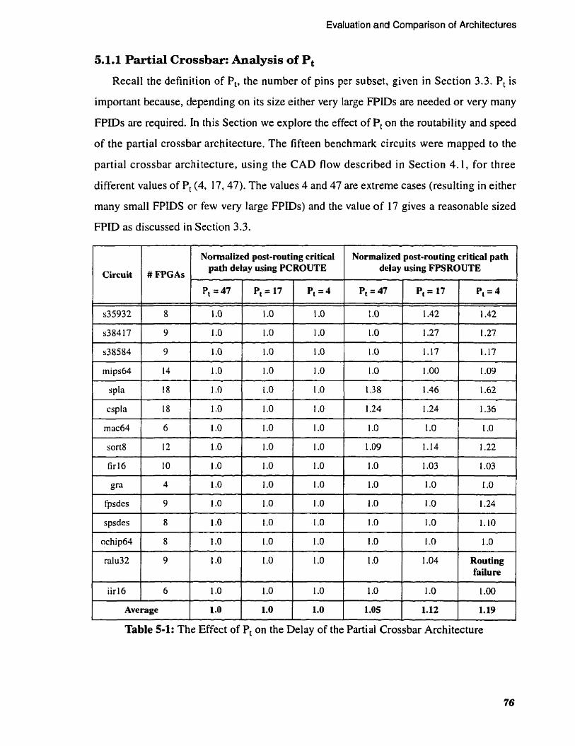
Evaluation and Comparison of Architectures
5.1.1 Partial Crossbar: Analysis of Pt
Recall the definition of P,, the number of pins per subset, given in Section 3.3. Pt is
important because, depending on its size either very large FPIDs are needed or very many
FPIDs are required. In this Section we explore the effect of Pt on the routability and speed
of the partial crossbar architecture. The fifteen benchmark circuits were mapped to the
partial crossbar architecture, using the CAD flow described in Section 4.1, for three
different values of P, (4, 17,47). The values 4 and 47 are extreme cases (resulting in either
many smali FPIDS or few very large FPIDs) and the value of 17 gives a reasonable sized
FPID as discussed in Section 3.3.
1 1 1 Norrnalized pst-routing critical 1 Normalized post-muting critical path ( 1 Circuit 1 X FPGAr
~ ~35932
s384 17
~38584
mi ps64
spla
cspla
m ac64
sort8
fir16
fpsdes
spsdes
ochip64
rzilu32
i ir l6
path delay using PCROUTE , -
1 1
delay using FPSROUTE 1 I
Table 5-1: The Effect of P, on the Delay of the Partial Crossbar Architecture
8
9
9
14
18
18
6
12
1 O
4
9
8
8
9
6
Average
P , = 4 7 5
1 .O
1 .O
1 .O - 1 .O
1 .O
1 .O
1 .O -
1 .O
1 .O
1 .O
1 .O
1 .O
1 .O
1 .O
1 .O
1.0
P,=17 - - - - 1 .O
1 .O
1 .O
1 .O
I .O
1 .O
1 .O
I .O
1 .O
1 .O
1 .O
1 .O
1 .O
1 .O
1 .O
1.0
Pt = 4 - - -
1 .O
1 .O
1 .O
1 .O
I .O
1 .O
1 .O
1 .O
1 .O
1 .O
1 .O
1 .O
1 .O
1 .O
1 .O
1.0
Pt = 47
1 .O
1 .O
1 .O
1 .O
1.38
1.24
1 .O
1 .O9
1 .O
1 .O
1 .O
1 .O
1 .O
1 .O
1 .O
1 .OS
1.42
1.27
1.17
1 .O0
1.46
1.24
1 .O
1.14
1 .O3
1 .O
1 .O
1 .O
1 .O
1 .O4
1 .O
1.12
1.42
1.27
1 .17
1 .O9
1.62
1.36
1 .O
1.22
1 .O3
1 .O
1.24
1.10
1 .O
Routing Mure
1.00
1.19

Evaluation and Cornparison of Architectures
We used two routing algorithms to do these experiments: FPSROUTE (described in
Section 4.4.4). which employed a somewhat generic maze-routing algorithm, and
PCROUTE (described i n Section 4.4.4). which used a algorithm that specifically
addressed the nature of a partial crossbar.
The effect of P, on the critical path delay of the partial crossbar is shown in Table 5- 1.
The first column shows the circuit nüme. The second column gives the number of FPGAs
needed to implement the circuit. PCROUTE gives the same critical path delay value for
each circuit for al1 three values of P,. Therefore, the critical path delay obtained by
PCROUTE is set as I . Columns 3 to 5 show the normalized post-routing critical path
delay obtuined for the circuit using PCROUTE for the three values of Pt. The columns 4 to
6 show the normalized post-routing critical path delay obtained using FPSROUTE for the
three values of Pt. Table B-3 in Appendix B is similar to Table 5-1 except that it shows the
actual (un-normalized) critical path delay values.
The first clear conclusion is that Pt has no impact on the routability of the partial
crossbar, because al1 the circuits were routable by PCROUTE for al1 the Pt values used.
The same was true for FPSROUTE as well except for the routing failure in one circuit
(rahi32) for the Pt = 4 case. An interesting point that follows from this conclusion is that
we do not need connections between FPIDs, as proposed in [Icub94], to improve the
routability of the partial crossbar.
Observe that the PCROUTE algorithm, which is tuned for the partial crossbar
architecture, gives the same delay value irrespective of the value of P,. This shows that it is
able to tackle the increased complexity of the routing task when we use very small values
of Pt with no adverse effects on routability or speed.
We include the results for FPSROUTE to wam of the danger of using an inappropriate
algorithm for the partial crossbar: here the effect of Pt on speed is quite significant, the
delay increases as the value of P, decreases. For P, = 4, average increase in delay using
FPSROUTE is 19% across al1 circuits, and 62% more in the worst case.
The partial crossbar is a very robust architecture that allows us to use a wide range of
Pt values without any penalties on routability and speed.

Evaluation and Cornparison of Architectures
7g nets routcd
Figure 5-1: The Effect of Pp on the Routability of the HCGP Architecture
We wil l use P, = 17 when comparing the partial crossbar to the other routing
architectures because this value gives good routabili ty and speed and requires reasonable
sized FPIDs.
5.1.2 HCGP Architecture: Analysis of Pp
Recall the definition of Pp, given in Section 3.4.1, which is the percentage of pins per
FPGA used for programmable connections in the hybrid architectures. Pp is important
because it potentially affects the cost, routability and speed of the hybrid architectures. If
Pp is too high it will lead to increased pin cost because more programmable connections
are required. If Pp is too low it may adversely affect the routability.
Here we explore the effect of Pp on the routability and speed of the HCGP
architecture. We mapped the fifteen benchmark circuits to the HCGP architecture using
five different values of Pp (20, 30, 40, 50, 60). We do not route for other values of Pp
because we believe that would need greater time and effort without giving more accurate
results. For example, it is most likely that the percentage of nets routed at Pp = 55% would

Evaluation and Cornparison of Architectures
be in between the percentage of nets obtained at Pp = 50% and Pp = 60%. The results are
shown in Figure 5-1, in which the Y-axis represents the percentage of inter-FPGA nets
successfully routed for each circuit and the X-axis represents Pp. The first clear conclusion
is that PI, = 60% gives 100% routability for al1 the benchmark circuits. Notice that about
two thirds of the circuits routed at Pp I 40%, and for the remaining one third, more than
97% of the nets routed. This implies that there is a potential for obtaining 100% routability
for al1 circuits at Pp = 40% if we use a routability driven partitioner like the one used in
[Kim96]. We believe this will lead to further reduced pin cost for the HCGP architecture,
but leave it as an area for future work.
We conjecture that the P, velue required for routing completion of a given circuit on
the HCGP depends upon how well the circuit structure 'matches' the topology of the
architecture.
I I Post Routing Critical Path Delay (ns) I
We also investigated the effects of Pp on the post-routing critical path delay. Table 5-2
Circuit
~35932
s384 17
~38584
sort8
firl6
gra
fpsdes
spsdcs
ochip64
3 1 6
shows the ten circuits that routed for Pp < 60%. The first column shows the circuit name.
In subsequent columns, the critical path delay of each circuit for different values of Pp (20,
Table 5-2: The Effect of on the Delay of the HCGP Architecture
P, = 20
unroutablc
87
unroutablc
unroutabk
147
57
30, 40, 50, 60) is shown. A surprising conclusion is that overall, the lower PD values have
P, = 30
unroutablc
94
96
unroutable
160
57
Pp = 40
5 3
94
96
unroutablc
163
57
unroutablc
unroutable
50
143
176
192
50
133
173
unroutable
50
143
Pp = 50
5 3
94
98
460
167
57
Pp = 60
53
94
98
499
167
57
176
205
50
152
176 - 205
50
152 a

Evaluation and Cornparison of Architectures
no significant effect on the critical path delay. Compared to the delay value at Pp = 60%,
for lower Pp values, the delay either remained the same or decreased slightly (only 4% less
on average and 12% less in the best case).
For the circuits in which the delay was reduced, a s Pp decreased one or more
programmable connections on the critical paths were replaced by the more plentiful and
faster hardwired connections. Note that as P, is reduced, more hardwired connections are
available. For circuits in which the delay remained the same, 'segments' on the critical
path are part of very high fanout nets that have to be routed using FPIDs because of the
lack of free pins i n FPGAs. These free pins are required for routing multi-terminal nets
using only hardwired connections. Therefore, even though more hardwired connections
are available at lower values of P,, they cannot be used for routing the multi-terminal nets
on the critical path.
We will use Pp = 60% when comparing the HCGP to the other routing architectures
because this value gives good routability and speed.
5.1.3 HTP Architecture: Analysis of Pp
We also explored the effect of Pp on the routability of the Hybrid Torus
Partial-Crossbar (HTP) architecture. As in the case of HCGP, the fifteen benchmark
circuits were mapped to the HTP architecture using five different values of Pp. The results
are shown in Figure 5-2, where the Y-axis represents the percentage of inter-FPGA nets
routed and the X-axis represents Pp. As in the case of HCGP, PI, = 60% gives 100%
routability across al1 circuits. The routability of the HTP architecture, however, is not as
good as that of the HCGP architecture. Comparing Figure 5- 1 and Figure 5-2, the average
percentage of nets routed across al1 the circuits is higher for the HCGP compared to the
HTP architecture. For example, the percentage of nets routed for al1 circuits for Pp = 30%
ranges from 93% to 100% for HCGP, compared to 86% to 100% for HTP.
5.1.4 HWCP Architecture: Analysis of Pp and Cs
Recall from Section 3.4.3 that in the Hardwired-Clusters Partial Crossbar (HWCP)
architecture, the FPGAs are grouped into clusters whose size is represented by a parameter
called the cluster size (Cs). All the FPGAs within each cluster are connected to each other
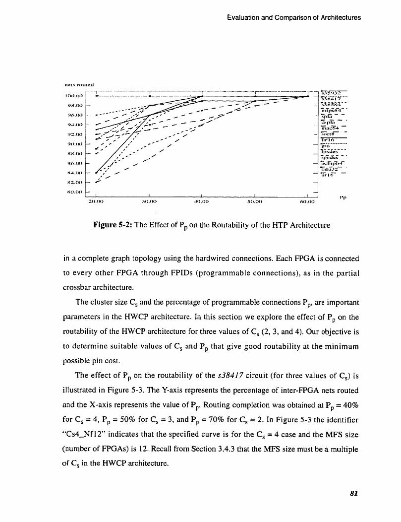
Evaluation and Cornparison of Architectures
Figure 5-2: The Effect of Pp on the Routability of the HTP Architecture
in a complete graph topology using the hardwired connections. Each FPGA is connected
to every other FPGA through FPlDs (programmable connections), as in the partial
crossbar architecture.
The cluster size Cs and the percentage of programmable connections Pp, are important
parameters in the HWCP architecture. In this section we explore the effect of Pp on the
routability of the HWCP architecture for three values of Cs (2, 3, and 4). Our objective is
to determine suitable values of Cs and Pp that give good routability at the minimum
possible pin cost.
The effect of Pp on the routability of the $38417 circuit (for three values of C s ) is
illustrated in Figure 5-3. The Y-axis represents the percentage of inter-FPGA nets routed
and the X-axis represents the value of Pp. Routing completion was obtained ai Pp = 40%
for Cs = 4, Pp = 50% for Cs = 3, and Pp = 70% for Cs = 2. In Figure 5-3 the identifier
"Cs4-Nfl2" indicates that the specified curve is for the Cs = 4 case and the MFS size
(number of FPGAs) is 12. Recall from Section 3.4.3 that the MFS size must be a multiple
of Cs in the HWCP architecture.

Evaluation and Cornparison of Architectures
% of inter-FPGA nets rauted
Figure 5-3: The Effect of P,, on Routability of HWCP Architecture (~38417 circuit)
The Pp values required for routing completion across al1 circuits for the three values of
Cs, are shown in Table 5-3. The first coiumn shows the circuit name and the second
column shows the number of FPGAs needed to fit the circuit on HWCP for the three
values of Cs. The third column shows the minimum value of Pp required for routing
completion of the circuit in HWCP for three values of Cs. The results from Figure 5-3 and
Table 5-3 show that the best routability results for the HWCP architecture (with the lowest
possible Pp value to minimize the pin cost) are obtained when Cs = 4 and Pp = 60%. The
percentage of circuits that routed for Pp 5 60% were 20% for Cs = 2, 60% for Cs = 3 and
80% for Cs = 4.
Table 5-3: The Minimum Pp Value Required for Routing Completion in HWCP
82
Circuit
~35932
s384 17
Numbcr of FPGAs
cs=2
8
10
Minimum value of Pp required for routing completion
Cs = 2
70
70
cs=3
9
9
C,=4
8
12
Cs = 3
60
50
Cs = 4
60
40

Evaluation and Comparison of Architectures
Circuit l I Number of FPGAs Minimum value of Pp required for
routing completion
Table 5-3: The Minimum PI, Value Required for Routing Completion in HWCP
~38584
mips64
spla
cspla
rnac64
sort8
tir 16
Ers
fpsdcs
spsdcs
ochip64
ralu32
iir 16
The clear conclusion from these results is that Cs = 4 and Pp = 60% are suitable
choices for achieving good routability at the minimum possible pin cost in the HWCP
architecture. Note that we did not get routing completion in the HWCP architecture for 3
out of 15 circuits. Although we did not explore the routability of HWCP for Cs > 4, we
expect that it will continue to improve as Cs increases relative to the MFS size. Note that
when Cs equals the MFS size, the HWCP architecture reduces to the HCGP architecture.
For Pp = 100%, the HWCP architecture reduces to the partial crossbar architecture.
5.2 Comparison of 8-way Mesh and Partial Crossbar Architectures
In this section we compare the 8-way mesh architecture with the partial crossbar.
Table 5-4 presents the results obtained after mapping fifteen benchmark circuits to the
Number of circuits routed at Pp 560%
c,=2
1 O
16
18
18
6
14
10
4
10
8
8
16
6
Cs= 2
70
80
1 O0
1 O0
80
70
70
60
70
70
40
1 O0
50
cs=3
9
15
18
18
6
15
12
6
9
9
9
15
6
3 of 15 (20%)
C,=4
12
16
20
20
8
16
12
4
12
8
8
16
8
Cs = 3
60
70
100
1 O0
50
70
40
40
60
60
40
80
40
Cs = 4
60
60
100
100
60
60
40
20
40
60
20 - 70
40
9 of 15 (60%)
12 of 15 (80%)

Evaluation and Cornparison of Architectures
8-way mesh and partial crossbar architectures. The first column shows the circuit name,
the second column shows the number of FPGAs needed to implernent the circuit, and the
third column shows percentage of nets routed, in each architecture. The fourth and fifth
columns show pin cost (defined in Section 4.2.1) and post-routing critical path delay
(defined in Section 4.2.2) respectively, obtained for each architecture.
Recall from Section 3.3 and Section 5.1.1 that we set Pt = 17 in al1 experiments for
cornparing the partial crossbar to the other architectures.
Notice that the partial crossbar is always routable after the first partitioning atteinpt for
each circuit. Only five of the fifteen benchmark circuits were routable on the 8-way mesh
even after mapping attempts with increased array sizes. The fact that so few circuits
successfull y routed indicates a basic flaw with the rnesh architectures.
The mesh architectures failed for the majority of circuits due to a number of reasons.
First, the locality available in inter-FPGA netlists for real circuits is not great enough for
the nearest neighbor connections. Second, there are not enough free pins available for
routing the non-local and rnulti-terminal nets. Routing such nets uses up many free pins in
FPGAs. For example, consider the routing of non-local and multi-terminal nets illustrated
in Figure 5-4. A non-local two-terminal net uses up pins in the intermediate FPGA as
illustrated in Figure 5-4(a). This problem becomes worse as the array size increases.
Multi-terminal net routing requires extra FPGA pins to connect the source to multiple
Pin cost
Circuit
Post-routing critical path delay
(in ns.) Number of FPGAs
Table 54: Cornpaison of the 8-way Mesh and Partial Crossbar Architectures
% nets routed
~35932
~38417
~38584
mips64
spla
8-wa y mes h
12 (3 X 4)
12 (3 X 4)
30 (5 X 6)
> 48 (6 X 8)
>48 ( 6 x 8 )
Par. Cross.
8
9
9
14
18
8-way mesh
1 O0
1 O0
1 00
92
90
Par. Cross.
1 O0
1 O0
1 O0
1 00
100
8-way mesh
2304
2304
5760
> 9216
> 92 16
Par. Cross.
3428
3 807
3 807
5646
72 1 8
8-way mes h
51
124
217
Rout. fail- ure
Rout. fail- ure
Par. Cross.
57
94
139
462
196

Evaluation and Comparison of Architectures
Table 5-4: Comparison of the 8-way Mesh and Partial Crossbar Architectures
Circuit
sinks as depicted in Figure 5-4(b). The problem becomes more severe as the net fanout
increases.
It was initially surprising to find no success when the mesh size was expanded in an
atternpt to obtain routing completion. Clearly the larger mesh has more free pins.
However, since the array is larger, this in tum leads to an increase in average wire length
and more in ter-FPGA nets, partial ly nulli fy ing the advan tage of increased free pins.
These results show the partial crossbar architecture is superior to the 8-way mesh
architecture.
The delay results show that for srnall array sizes, the 8-way mesh gives better speed
than the partial crossbar (for the circuits $35932, gra and ochip64). This is because some
Number of FPGAs
8-way mesh
csplri
mm64
sor t8
firl6
g r a
f'psdes
spsdcs
ochip64
d u 3 2
iirl6
P r . Cross.
% nets routed
8-way mesh
8 5
77
80
96
1 O0
8 8
84
1 00
8 7
8 9
Avg.: 91.2
> 4 0 ( 5 X 8 )
> 18 (3 X 6)
> 28 (4 X 7)
> 2 5 ( 5 X 5 )
4 (2 X 2)
> 18 (3 X 6)
> 15 (3 X 5)
8 ( 2 X 4 )
> 30 (5 X 6)
> 15 (3 XS)
iîvg.: > 23
Par. Cross.
1 O0
1 O0
IO0
1 O0
1 O0
100
1 O0
100
100
1 O0
Avg.: 100
Pin cost
18
6
12
10
4
9
8
8
9
6
Avg: 10
8-way mcsh
C -
>7680
> 3456
> 5376
> 4800
76 8
> 3456
> 2880
1536
>5760
> 2880
Total: > 67392
Post-mutina critical path delay
(in ns.)
Par. Cross.
7218
2760
4944
4944
1912
3807
3428
3428
3807
2760
Total: 62914
8-way mesh
Rout.fai1- u re
Rout. fail- u re
Rout. fail- ure
Rout. fail- urc
60
Rout. f d - ure
Rout. fail- urc
47
Rout.fail- urc
Rout. fail- ure
Par. Cross. d
193
623
533
238
70
2 2 7
249
63
317
160

Evaluation and Comparison of Architectures
FPGA FPGA
FPGA
I I
sink sink FPGA . FPGA FPGA
Figure5-4: Routing in the Mesh (a) Non-local Net (b) Multi-terminal Net
or al1 the nets on the critical paths may utilize direct connections between FPGAs that are
faster than connections that go via FPIDs. But the speed deteriorates as the array sizes get
bigger, because the critical nets travel through many FPGAs.
With respect to cost, for the same number of FPGAs, the partial crossbar always needs
twice as many pins as an 8-way mesh. For 4 out of 15 circuits the 8-way mesh has less pin
cost compared to the partial crossbar architecture. On average across al1 the circuits, the
pin cost will be more for the 8-way mesh. This is because of the very large array sizes that
will be reqiiired to make many circiiits routable on the 8-way mesh.
Mesh architectures should be avoided if the goal is to implement a wide variety of
circuits on MFSs. Although meshes and linear arrays have been used successfully in
practice [Arno92, Vui196J. they were successful only for implemen ting algorithms that
match the mesh topology, which implies they require mostly nearest neighbour type of
connections between FPGAs. We also note that meshes can be used successfully when the
FPGA pins are time division multiplexed [Babb97], but this results in a substantial
reduction in speed.
FPGA -
5.3 Comparison of HCGP and Partial Crossbar
FPGA
In this section we compare the HCGP architecture to the partial crossbar architecture.
The benchmark circuits were mapped to the partial crossbar and HCGP architectures
using the experimental procedure described in Section 4.1. The results obtained are shown
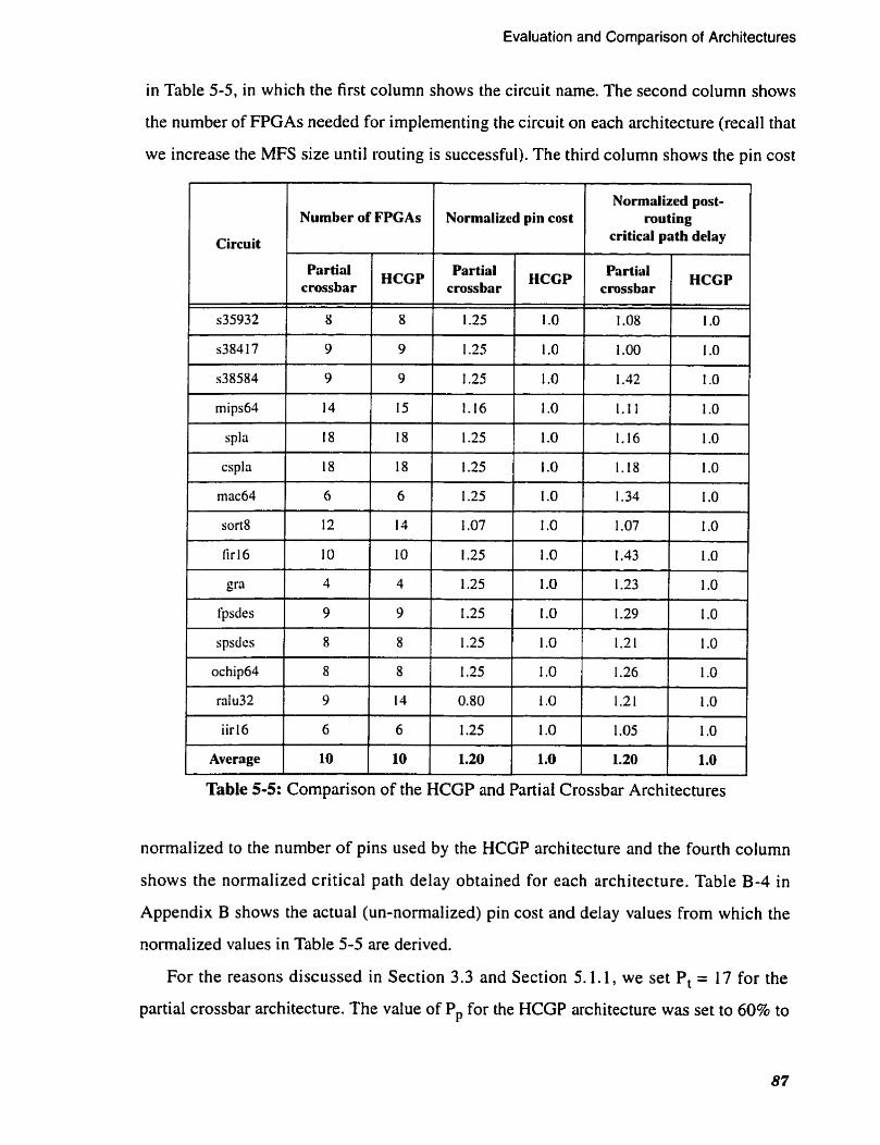
Evaluation and Comparison of Architectures
in Table 5-5, in which the first column shows the circuit name. The second column shows
the number of FPGAs needed for implementing the circuit on each architecture (recall that
we increase the MFS size until routing is successful). The third column shows the pin cost
I Circuit I 1 critical path delay 1 Number of FPGAs
Table 5-5: Comparison of the HCGP and Partial Crossbar Architectures
Normalizcd pin cost
~35932
s384 17
~38584
mips64
spla
csplri
111x64
sort8
fir 16
Srri
fpsdes
spsdcs
ochip64
raIu32
iirl6
Average
normalized to the nurnber of pins used by the HCGP architecture and the fourth column
shows the normalized critical path delay obtained for each architecture. Table B-4 in
Appendix B shows the actual (un-normalized) pin cost and delay values from which the
normalized values in Table 5-5 are derived.
For the reasons discussed in Section 3.3 and Section 5.1.1, we set Pt = 17 for the
partial crossbar architecture. The value of Pp for the HCGP architecture was set to 60% to
Normalized post- routing
Partial crossbar
8
9
9
14
18
18
6
12
1 O
4
9
8
8
9
6
10
Partial cmssbar
1 .O8
1 .O0
1.42
1.1 1
1.16
1.18
1.34
1 .O7
1.43
1.23
1.29
1.2 1
1.26
1.21
1 .O5
1.20
HCGP
8
9
9
15
18
18
6
13
10
4
9
8
8
14
6
10
HCGP
1 .O
1 .O
1 .O
1 .O
1 .O
1 .O
1 .O
1 .O
1 .O
1 .O
1 .O
1 .O
1 .O
1 .O
1 .O
1 .O
Partial crossbar
1.25
1.25
1.25
1.16
1.25
1.25
1.25
1 .O7
1.25
1.25
t .25
1.25
1 .25
O. 80
1.25
1.20
HCGP
1 .O
1 .O
I .O
1 .O
1 .O
1 .O
1 .O
I .O
f .O
1 .O
I .O
1 .O
1 .O
1 .O
1 .O
1.0

Evaluation and Cornparison of Architectures
obtain good routability across al1 circuits, as discussed in Section 5.1.2. Notice that the
parameter Pt also applies to the programmable connections in the HCGP. For the same
reasons as in the partial crossbar, we chose P, = 14 for the HCGP architecture.
In reviewing Table 5-5, consider the circuit mips64. The first partitioning attempt
resulted in 14 FPGAs required to implement the circuit on the partial crossbar. However,
the circuit was not routable on the HCGP and the partitioning was repeated after reducing
the number of pins per FPGA specified to the partitioner by 5%. This resulted in 15
FPGAs required to implement the circuit. The second partitioning atternpt was routable on
the HCGP architecture because more 'free pins' were available in each FPGA for routing
purposes. The pin cost for the partial crossbar was still more than that for the HCGP
because i t uses many more programmable connections, and hence more FPID pins. A
partial crossbar always requires one FPID pin for every FPGA pin; the HCGP architecture
requires a lower ratio, (0.6: 1) as implied by the setting of the parameter PI, = 60%.
Inspecting Table 5-5, we can make several observations. First, the partial crossbar
needs 20% more pins on average, and as much as 25% more pins compared to the HCGP
architecture. Clearl y, the HCGP architecture is superior to the partial crossbar arc hi tecture
in terms of the pin cost metric. This is because the HCGP exploits direct connections
between FPGAs to save FPID pins that would have been needed to route certain nets in the
partial crossbar. However, for routability purposes, the HCGP needs some free pins in
each FPGA and may require repeated partitioning attempts for some circuits.
Table 5-5 also shows that the typical circuit delay is lower with the HCGP
architecture: the HCGP gives significantly less delay for twelve circuits compared to the
partial crossbar and about the sarne delay for the rest of the circuits. The reason is that the
HCGP u tilizes fast and direct connections between FPGAs, whenever possible. From the
delay values in Table 4-3, we can show that the interconnection delay is much smaller
(12.6 ns) if we use direct connections between FPGAs compared to the delay vaiue (25.6
ns) when connecting two FPGAs through an FPID. Another interesting observation is that
even for the circuits where the HCGP needs more FPGAs compared to the partial crossbar,
it still gives comparable or better delay value. This clearly demonstrates that the HCGP

Evaluation and Cornparison of Architectures
architecture is inherently faster due to the faster hardwired connections. It gives a
significant speed advantrige, especially when we use timing driven inter-FPGA routing.
The superior speed of the HCGP architecture can be potentially crucial to ASIC
designers who use MFSs as simulation accelerators, to mn test vectors on ASIC designs.
According to one designer [Mont98], even a 10% increase in clock speed is very useful
because it enables the designers to mn many more test vectors in the sarne amount of time,
thus improving the design quality and reliability.
Comparison of HTP and HCGP Architectures
A comparison of the HTP and HCGP architectures is presented in Table 5-6, which
has a format similar to Table 5-5. Table B-5 in Appendix B is similar to Table 5-6 except
that it shows the actual (un-nomalized) pin cost and delay values.
Across d l circuits, the HTP architecture needs 13% more pins on average, and as
much as 74% more, compared to the HCGP architecture. The HCGP architecture is
superior to HTP because i t has better routing flexibility. The hardwired connections are
utilized more efficiently in the complete graph topology (used in the HCGP) compared to
the toms topology (used in the HTP). For example, in the HCGP the shortest path between
any pair of FPGAs can be obtained by utilizing any intemediate FPGA outside the pair. In
HTP HCGP HTP HCGP
~35932 9 8 1.12 1 .O
Circuit
- -
cspla 25 18 1.39 1 .O
Table 5-6: Comparison of the HTP and HCG
Normalized post-routing critical path
delay
Number of FPGAs
P Architectures
Normalized pin cost
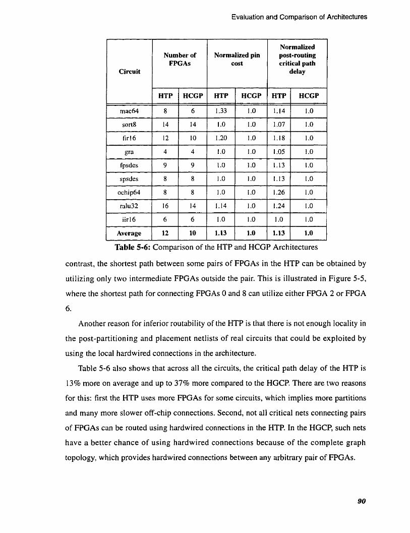
Evaluation and Comparison of Architectures
contrat, the shortest path between some pairs of FPGAs in the HTP can be obtained by
utilizing only two intermediate FPGAs outside the pair. This is illustrated in Figure 5-5,
Circuit
mac64
sort8
fir!6
gr3
fpsdes
spsdes
ochip64
raIu32
iirl6
Average
where the shonest path for connecting FPGAs O and 8 can utilize either FPGA 2 or FPGA
Table 5-6: Comparison of the HTP and HCGP Architectures
Normalized post-routing critical path
delay
Another reason for inferior routability of the HTP is tliat there is not enough locality in
HTP
1.14
1 .O7
1.18
1 .O5
1.13
1.13
1.26
1.24
1 .O
1.13
the post-partitioning and placement netlists of real circuits that could be exploited by
Number of FPGAs
HCGP
1 .O
1 .O
1 .O
1 .O
1 .O
1 .O
1 .O
1 .O
1 .O
1 .O
using the local hardwired connections in the architecture.
HTP
8
14
12
4
9
8
8
16
6
12
Normdized pin cost
Table 5-6 also shows that across al1 the circuits, the criiical path delay of the HTP is
HCGP
6
14
10
4
9
8
8
14
6
10
HTP
1.33
1 .O
1 20
1 .O
1 .O
1 .O
1 .O
1.14
1 .O
1.13
13% more on average and up to 37% more compared to the HGCP. There are two reasons
HCGP
1 .O
1 .O
1 .O
1 .O
1 .O
1 .O
1 .O
1 .O
1 .O
1 .O
for this: first the HTP uses more FPGAs for some circuits, which implies more partitions
and many more slower off-chip connections. Second, not al1 critical nets connecting pairs
of FPGAs cm be routed using hardwired connections in the HTP. In the HGCP, such nets
have a better chance of using hardwired connections because of the complete graph
topology, which provides hardwired connections between any arbitrary pair of FPGAs.

Evaluation and Comparison of Architectures
Figure 5-5: Hardwired connections in the HTP architecture
I m
HTP Compared to the Partial Crossbar
Comparing the average pin cost and critical path delay for HTP and partial crossbar
architectures (relative to the HCGP architecture) from Table 5-6 and Table 5-5, we crin
conclude that the HTP architecture is rnarginally better than the partial crossbar. Across al1
circuits, the average pin cost as well as delay is 13% more for HTP (relative to HCGP), in
C
contrast to the partial crossbar in which the average pin cost as well as delay is 20% more
(relative to HCGP).
I I I
FPGA 1
FPGA O
5.5 Comparison of HWCP and HCGP Architectures
RecaIl from Section 3 . 4 3 that the HWCP is a hierarchical architecture in which the
FPGA 2
FPGAs are divided into clusters and the FPGAs within each cluster are connected using a
3
complete graph topology. Also recall that the motivation behind this architecture is to
combine the routability and speed advantages of the HCGP architecture with easier
manufacturability. To investigate the efficacy of the HWCP architecture in meeting the
design goals, we mapped the benchmark circuits to this architecture and compared it to the
HCGP architecture. We set Pp = 60% and Cs = 4 for the HWCP architecture to obtain good
routability as discussed in Section S. 1.4.
The mapping results are shown in Table 5-7. Table B-6 in Appendix B is similar to
Table 5-7 except that it shows the actual (un-normalized) pin cost and critical path delay
values.

Evaluation and Comparison of Architectures
Number of FPGAs
- -- -- --
Table 5-7: Comparison of the HWCP and the HCGP Architectures
Table 5-7 shows that the HWCP architecture failed to route three of the fifteen
benchmark circuits. For the twelve circuits that routed on the HWCP, the pin cost is 17%
more on average, and up to 33% more compared to the HCGP architecture. The increase
in pin cost is partly due to the fact that the HWCP required more FPGAs for some circuits
to make the MFS size (measured by the number of FPGAs) a multiple of the cluster size
(Cs = 4). The other reason is that the HCGP has superior routability compared to HWCP.
Circuit
~35932
s38-117
~38584
mips64
spla
cspla
mac64
sort8
firi6
Ira
fpsdes
spsdes
ochip64
ralu32
iir 16
Norrnalized pin cost Normalized post-
routing critical path delay
HWCP (Cs = 4)
8
12
12
16
20
20
8
16
12
4
12
8
8
16
8
Average
HCGP
8
9
9
15
18
18
6
14
1 O
4
9
8
8
14
G
HWCP (Cs = 4)
1 .O
1.33
1.33
1 .O7
routing failure
routing failure
1.33
1.14
1.20
1 .O
1.33
1 .O
1 .O
routing failure
1.33
12
HCGP
1 .O
1 .O
1 .O
1 .O
I .O
1 .O
1 .O
1 .O
1 .O
1 .O
1 .O
1 .O
1 .O
1 .O
1 .O
(Cs =4)
1 .O8
1.18
1.20
0.99
routing fai 1 ure
routing failure
1.15
1.15
1.19
1 .O
1 -29
1.15
1.26
routing friilure
1.1 1
HCGP
1 .O
1 .O
1 .O
1 .O
I .O
1 .O
1 .O
I .O
1 .O
1 .O
i .O
1 .O
1 .O
1 .O
1 .O
10 1.17 1.0 1.15 1.0

Evaluation and Cornparison of Architectures
For the twelve circuits that routed on HWCP, the critical path delay is 15% more on
average, and up to 29% more compared to the HCGP architecture. The reasons for this
are: first the HWCP uses more FPGAs for some circuits, which implies more partitions
and many more slow off-chip connections, some of which may lie on the critical path.
Second, unlike the HCGP not al1 critical nets connecting pairs of FPGAs can be routed
using hardwired connections in the HWCP.
Despite some routing failures, the routability results for HWCP are quite encouraging
for the following reasons: first, we did not try higher cluster sizes (relative to the MFS
size). Recall from Section 5.1.4 that the routability of the HWCP architecture improves
with the increase in cluster size. Second, the partitioning and placement niethods used for
the HWCP architecture were not the best possible. Architecture-driven partitioning and
placement methods may give better routability results.
Due to the reasons given above, we conclude that the HWCP architecture has the
potential to provide good routabi lity, speed, and manufacturability. Unlike the HCGP
architecture which is the most suitable for single-board MFSs, HWCP lends itself to
hierarchical implementations of large MFSs that use hundreds of FPGAs distributed
across multiple boards. Such large MFSs are currently used for emulating complex ASICs
and microprocessors [Quic98].
HWCP Compared to HTP Comparing the average pin cost and critical path delay for HWCP and HTP
architectures (relative to the HCGP architectures) from Table 5-6 and Table 5-7, we can
conclude that the HTP is marginally better than the HWCP. Across al1 circuits, the average
pin cost for HTP is 1.13 (compared to 1.17 for HWCP) and the average delay is 1.13
(compared to 1.15 for HWCP). Moreover, HTP obtained 100% routability across al1
circuits in contrast to HWCP which failed to route three circuits. While it is possible that
larger cluster sizes may irnprove the results for HWCP, it is also likely that better
locality-enhancing partitioning tools wil l further improve the results for HTP. To
conclude, for large hierarchical MFSs, both HTP and HWCP architectures should be
investigated to determine which architecture gives the best results. From the results
Evaluation and Cornparison of Architectures
obtained in Our research, both architectures seem to be prornising candidates for large
MFSs.
Several MFS routing architectures were evaluated and compared in this chapter. An
experimental approach was used and real benchrnark circuits were employed. The
architectures were compared on the basis of pin cost and post-routing critical path delay
metrics.
The key parameters associated with the partial crossbar and the hybrid architectures
were explored. The partial crossbar is a very robust architecture because the effect of
varying a key architecture parameter (P,) on the routability, speed, and cost is minor. This
is contingent, however, on using an appropriate inter-FPGA routing algorithm.
A key parameier associated with the hybrid architectures, Pp, was explored and it was
experirnentally determined that Pp = 60% gives good routability across al1 the benchmark
circuits. In the hybrid architecture HWCP, in addition to Pp, the cluster size Cs is an
important parameter. We experimentally determined that Cs = 4 gives good routability for
the HWCP architecture.
The partial crossbar is one of the best existing architectures and is the key technology
behind commercially available MFSs [Quic98]. We showed that the partial crossbar is
superior to the mesh architecture. The main reason behind inferior results for the mesh
architecture is that the FPGAs are used for both logic and inter-FPGA routing. This causes
routability problems that cannot be solved even after increasing the mesh size in order to
fit a circuit.
We showed that one of the newly proposed hybrid architectures, HCGP, is superior to
the partial crossbar. Across al1 the benchmark circuits, the pin cost of the partial crossbar
is on average 20% more than the new HCGP architecture and up to 25% more.
Furthemore, the critical path delay for the benchmark circuits implemented on the partial
crossbar were on average 20% more than the HCGP and up to 43% more.

Evaluation and Cornparison of Architectures
The HTP architecture was shown to be inferior to the HCGP and only marginally
better than the partial crossbar and the HWCP. The HWCP architecture was evaluated
compared to the HCGP architecture and gave encouraging routability and speed results.
From the scalability point of view, both HTP and HWCP architectures are suitable for
irnplernenting large MFSs implemented using multiple boards.
Overall, the results show ihat for single-board MFSs, the HGCP is the best among al1
the MFS routing architectures evaluated.
We end this Chapter with a cautionary note. The quality of the architectural results
obtained depends upon the quality of the CAD tools used. To obtain the best possible
results, we used the best possible tools that we could develop or acquire in the time
available. There is always a scope for improvements in the CAD tools. For example, it
would have been better to use architecture-driven partitioning and placement for
architectures that have some notion of adjacency, such as the mesh, HTP, and HWCP.
While there may be minor improvements in the routability and speed results, we do not
expect our architectural conclusions to change radically after using such tools. For
example, an architecture-driven partitioner was used to map circuits to the mesh
architecture i n [Kim96], but the results for the mesh were still significantly worst
compared to the other architectures evaluated, such as the partial crossbar and the
tri-partite graph.

Conclusions and Future Work
6.1 Dissertation Summary
In this dissertation we evaluated and compared existing as well as new MFS routing
architectures by using a rigorous experimental approach that employed real benchmark
circuits. This research provides new insight into the strengths and the weaknesses of some
popular existing routing architectures. New hybrid architectures, that use a mixture of
hardwired and programmable connections, were proposed and shown to be superior to one
of the best existing architectures.
In Chapter 3, al1 the MFS routing architectures explored in this research were
described. The architectures are the 8-way rnesh, the partial crossbar and the three hybrid
architectures, HTP, HCGP and HWCP. The architectural issues and assumptions that anse
when mapping real circuits to the architectures were discussed.
In Chapter 4, the experimental framework and the CAD tools used for mapping the
benc hmark circuits to di fferent architectures were described. The architecture evaluation
metrics (pin cost and post-routing critical path delay) were discussed and the benchmark
circuits used were presented. In this research, particular attention was paid to the
development of architecture-specific inter-FPGA routing algorithrns, which were
discussed in detail. A static timing analysis tool for measuring the speed performance of
Conclusions and Future Work
different MFS routing architectures was described and a timing-driven routing algorithm
for the hybrid architectures was presented.
Finally, in Chapter 5, key architecture evaluation and cornparison results and their
analysis were presented. The key parameters associated with the partial crossbar and the
hybrid architectures were explored. We showed that the partial crossbar, which is one of
the best existing architectures, is superior to the best mesh architecture. We showed that
one of the newly proposed hybrid architectures, HCGP, is superior to the partial crossbar.
Across al1 the benchmark circuits, the pin cost of the partial crossbar is on average 20%
more than the new HCGP architecture and 25% more in the worst case. Furthermore, the
critical path delay for the benchmark circuits implemented on the partial crossbar were on
average 20% more than the HCGP and 43% more in the worst case. The HTP architecture
was shown to be inferior to the HCGP and only marginally better than the partial crossbar.
The HWCP architecture was evaluated compared to the HCGP architecture and gave
encouraging routability and speed results.
6.2 Principal Contributions
The principal contributions of this dissertation are as follows:
We proposed hybrid architectures and demonstrated that they are superior to one of the best existing architectures. We explored a key parameter associated with the hybrid architectures (Pp) and experimentally determined its best value for obtaining good routability at the minimum possible pin cosi.
We showed that the Hybrid Complete-Graph Partial-Crossbar (HCGP) architecture provides significant reductions in pin cost and delay compared to the partial crossbar architecture.
We proposed the Hardwired-Clusters Partial-Crossbar (HWCP) and Hybrid Toms Partial-Crossbar (HTP) architectures that are potentially suitable for large MFSs implemented across multiple boards.
We developed an MFS static timing analysis tool that was used to estimate and compare the speed performance of different MFS architectures. To Our knowledge, this is the first time such detailed timing information has been used in the study of board-level MFS routing architectures.

Conclusions and Future Work
5. We developed a timing-driven (board-level) inter-FPGA router for the hybrid architectures that exploits the fast hardwired connections available to obtain good speed performance.
6. We developed a new (board-level) inter-FPGA routing algorithm for the partial crossbar architecture that gives excellent results for real benchmark circuits.
6.3 Future Work
In this section, we discuss promising topics for future research. Thesc are categorized
into two broad areas: CAD tools for MFSs and future research in MFS architectures.
6.3.1 CAD Tools for MFSs
Recall from Section 5.1.2 that in the HCGP architecture al1 the circuits routed at PI, =
60% and 97-100% of the nets routed across al1 the circuits for Pp = 40%. Also recall from
Section 3.4.1 that iower values of Pp imply reduced pin cost in the hybrid architectures. A
routability-driven partitioner may achieve routing completion for almost al1 circuits for
lower values of Pp.
It has been shown that instead of partitioning flat circuit netlists, if the circuit design
hierarchy information is exploited by the partitioning algorithm, significant reductions in
both the number of FPGAs and the cut size can be obtained [Behr96, Fang98J. Utilizing
such partitioning algorithms may lead to better routability in the hybrid architectures that
use low values of Pp (20-40%). This is because the reductions in cut size makes the
inter-FPGA routing problem easier, since more free pins are available for routing each
FPGA.
In addition to providing good quality results, the partitioning algorithms also need to
be very fast to exploit the reconfigurable nature of MFSs. If the circuit partitioning itself
takes hours or even a few days for very large circuits, the utility of MFSs will be very
limi ted.
A simple timing model is used in our MFS timing analyzer (MTA) that assumes a
constant net delay independent of fanout for both intra-FPGA and inter-FPGA nets. A
timing model that accurately estimates the net delay based on fanout should be
investigated. It would also be interesting to compare the speed estimate given by MTA

Conclusions and Future Work
with the actual speed performance obtained on some existing MFSs to evaluate the
accuracy of the timing analysis tool. Also, for hierarchical architectures that use multiple
boards, the timing mode1 would need to be modified to consider the inter-board routing
delay.
Although not covered in this dissertation, fast and effective high-lcvel synthesis tools
(in addition to layout synthesis tools) are indispensable for MFSs to achieve widespread
utility as custom cornputing machines and logic emulators [Ga1195, Knap96, Syno971.
6.3.2 Future MFS Routing Architecture Research
A major open problem in MFS architecture research is to find an effective architecture
for large MFSs that use hundreds of FPGAs spread out across multiple boards. The
hierarchical HWCP architecture is a first step in this direction. It is not clear, however, if
other topologies may give better results. For example, is it better to use inter-cluster
hardwired connections, in addition to intra-cluster hardwired connections? What would be
suitable values of Pp and Cs (relative to the MFS size) for such hierarchical architectures?
Suitable CAD tools and extremely large benchmark circuits will be needed to explore such
architectures.
The virtual wires time-multiplexing technique is used on the mesh architecture in
commercially available logic emulators [Ikos98]. One problem with the rnesh architecture
is that it is very inefficient and slow for routing non-local and multi-terminal nets (as
discussed in Section 5.2). Using the virtual wires technique on the other architectures such
as the HCGP and completely connected graph may give much better speed results
compared to the mesh.
The HCGP is a very versatile architecture for single-board MFSs that gives excellent
routability and speed for a variety of circuits. As the FPGA logic and pin capacities
continue to increase, it rnake sense to use single board systems using a few high capacity
FPGAs to avoid t h e problems sssociated with using high pin count connectors for
multi-board systems [Lewi98]. Except for high-end logic emulation, such systems would
cover most other applications in custom computing and rapid prototyping. A prototype
single board system based on the HCGP architecture should be developed and tested for

Conclusions and Future Work
different custom computing applications. It would be interesting to map the algorithrns
originally used with linear arrays and meshes [Anio92, Vuil961 to the HCGP and compare
the logic utilization and speed results.
Finally, the relationship between the best architecture and the implementation
technology used is crucial. In the future, if MCMs and high pin count FPGAs using
flip-chip technology [Lang51 become cornmonplace. radically different routing
architectures (in contrast to board-level MFS routing architectures) may be required.

Appendix A
The Effect of Fixed I/0 Pin Positioning on The Routability and
Speed of FPGAs
A.l Introduction
As discussed in Section 4.1.1, after board-level FPGA placement and inter-FPGA routing in
MFSs, the pin assignment in each FPGA is done randornly. The alternative, allowing the auto-
matic placement and routing software the freedom to choose whichever pins it deems best for
each signal, may result in better routability and speed but is not feasible in many applications.
When developing an MFS architecture, it is important to know the effect of the fixed pin
assignment on the system's speed and rouiabili ty.
This question is also important in many other applications where FPGAs are used. For exam-
ple, when systems designers have already committed to the board-level layout, which dictates the
pin-signal assignment, and then wish to change the functionaiity of the FPGA. Although the orig-
inal pin assignment may have been chosen by the software, the subsequent assignment must
remain the same. If major delay increases result from fixing the pin locations in the second itera-
tion, or if routability disappears, then designers will need to account for these likelihoods in the
original design.
Anecdotal evidence [Chan93b] Boe1941 suggests that pre-assigning FPGA package pins
before placement and routing can adversely affect the speed and routability of several manufac-
turer's FPGAs. The speed and routability of an FPGA under pin constraints is a function of both
the routing architecture of the device (whether or not there are sufficient paths from the pads to al1
parts of the logic), and the quality of the placement and routing tools (how cleverly it organizes
the placement to overcome a difficult pin placement). In this Appendix, we are concemed with the
combined effect of routing architecture and automatic layout tools on specific commercial archi-
tectures. We present experimental results on the effect of fixed-pin assignment on FPGA delay
and routability. To our knowledge, no such formal study has yet been done. These results are for
the Xilinx XC4000 and the Altera FLEX 8000 families of FPGAs. The results of this study were
ilsed in developing the architecture of the Transmogrifier-2, an MFS developed at the University
of Toronto [Lewi97, Lewi981.
This Appendix is organized as follows: In Section A.2 we present the methodology used in
this work. Research results and their analysis are presented in Section A.3. Although the focus is
on the effects of fixed pins on delay and routability, a number of interesting observations on other
FPGA design issues can also be deduced from the results. We conclude in Section A.4 with a few
remarks on the significance of the results obtained and relevant topics for future work.
A.2 Benchmark Circuits and Experimental Procedure
To determine the effect of fixed pin constraints we performed placement and routing on a set
of benchmark circuits with and without constraints. The benchmark circuits were obtained from
both the MCNC Logic Synthesis 199 1 [Yang9 11 suite, and from several FPGA designs done at the
University of Toronto.
The experimental procedure used in our investigation is illustrated in Figure A-1 for the Xil-
inx FPGAs and Figure A-2 for the Altera FPGAs. For the Xilinx FPGAs, each benchmark circuit
available in the Xilinx netlist formai (XNF), was technology mapped (called "partitioning" by
Xilinx), placed, and routed using the 5.1.0 version of Xilinx place and route tool PPR [Xili94ü].
For the Altera FPGAs, each benchmark circuit available in the Xilinx netlist format (XNF) was
mapped into the FLEX 8000 FPGAs by using the MAX+PLUS LI compiler. The compiler accepts
circuits described using many standard netlist formats, including XNF, and performs technology
independent logic optimization, technology mapping, placement, and routing [Alte94a]. To deter-
mine the effect of pin assignment, each circuit was processed under four types of pin constraints,
for both Xilinx and Altera FPGAs.
Benchmark circuit Pin constraints file
PPR A
Critical path dclay
+ LCA file
+ Statistics on routing
Static timing analysis
I resourccs uscd
Extraction of routing information
Figure A-1: Experimental Procedure for the Xilinx FPGAs
I
1. No pin constraints (referred to as npc in the sequel): Technology Mapping, placement
and routing was performed without pre-assigning (fixing) any signals to pins.
2. Same pin constraints (spc): The pin-signal assignment was fixed before the placement
and routing; the pin assignments were the same as those generated by the uncon-
strained placement and routing run (i.e. npc).
3. Bad pin constraints (bpc): The pin-signal assignment was fixed before the placement
and routing and the pin assignment was intentionally bad. Signals that were assigned
to adjacent pins by unconstrained placement and routing run were assigned to pins at
opposite ends of the FPGA chip.
4. Random pin constraints (rpc): The pin-signal assignment was fixed before the place-
ment and routing and signals were assigned to randomly generated pin numbers.
The output files after place and route were analyzed for worst-case delay and utilization of
routing resources. The worst-case delay was determined using the static timing analysis tools
available in the Xilinx and Altera tool sets. For the Xilinx FPGAs, routing utilization was auto-
matically extracted from the output LCA file using a C program specifically developed for this

Benchmark circuit Pin constraints file
PPR
MAXiPLUS II Campilcr c
Static timing analysis a Critical path delay 1
Extraciion of r iuthg information
Siatistics on routing rcsourccs used
Figure A-2: Experimen ta1 Procedure for the Al tera FPGAs
purpose. The latter measures the number of single-length segments, double-length segments and
long lines used by the Xilinx placement and routing tool PPR. For the Altera FPGAs routing utili-
zation statistics are available from the report file that is generated after each compilation run.
For the Xilinx FPGAs, for each of the above four pin constrûint cases, five PPR mns were per-
fomed and the average delay and the average routing utilization were used. This was done to
determine the consistency of the results. The annealing option in PPR was used to obtain different
placement and routing results, and hence different delay and routing statistics, for each PPR run.
For the Altera FPGAs, a single compilation run for each pin constraint case was sufficient. This is
because for a given circuit and pin constraint case, the compiler gives the same placement and
routing results for multiple compilation runs, presumably because it uses deterministic algorithms
for placement and routing and has no non-deierministic option.

A.3 Experimental Results and Analysis
In this section we present the result of the experiments. Delay and routability results are given
for 16 benchmark circuits for the Xilinx FPGAs and for 14 benchmark circuits for the Altera
FPGAs. The circuits are the same except for two circuits that utilized on-chip RAM that is avail-
able in the XC4000 FPGAs but not in the FLEX 8000 FPGAs.
FPGA Device
# Y 0 pins
- - 9 1
- 58
- 64
l
Avg. Crit. Path Delay (bpd
158.7 ns (+2.8%)
1 Circuit % of FPGA
Pins and CLBs used
Avg. Crit. Psth Delay (rpd
163.3 ns (+5.8%)
- dalu (ALU)
l
c 1 908 (Error
Corrcct Cc t)
mu1 ( 1 6-bit Mult)
Avg. Crit. Path Delay tnpd
40 1 O DPQ 160-5
4003 PC84-5
4008 PQ 160-5
Avg. Crit. Path Delay (spd
c 1 355 (Error
Corrcct Cct)
70% pins 100% CLBs 83% PCLBs
95% pins 100% CLBS 98% PCLBs
49% pins 100% CLBs 99% PCLBs
57% pins 100% CLBs 89% PCLBs
173 ns
c499 (Error
Corrcct Cct)
154.4 ns
133.4 ns
247.7 ns
65% pins 99% CLBs
55% PCLBs
155.8 ns (C 1%)
135.9 ns (+2%)
266.4 ns (+8%)
129.7 ns
cg80 (ALU + Control)
94% pins 56% CLBs
53% PCLBs
72.7 ns
--
lcdm (LCD Disp Controller)
sw-f 128 (Partial Vit- erbi Decod
76% pins 48% CLBs 30% PCLBs
96% pins 100% CLBs 86% PCLBs
91% PCLBs 1 I I I
109.1 ns
57.1 ns
73% pins 100% CLBs
sll96 (Logic)
78"0CLBs I I (-2%) (+ 10%) (+4%) 53% PCLBs
108 ns (- 1%)
59.1 ns (+3.5%)
32.78 ns
Table A-1: Critical Path Delay Under Different Pin Constraints for the Xilinx FPGAs
108.4 ns (0%)
66 ns (+ 15.6%)
42.9 ns (0%)
1 16.3 ns (+6.6%)
65.611s (+ 15.4%)
51.3 ns (+19.6%)
42 ns (0%)
Avg. Crit. # FPGA % of FPGA
Circuit *O Deviee Pins and CLBs used
Delay pins
(npd
s 1423 24 4003 39% pins 262.5 ns (Logic) PC84-5 100% CLBs
90% PCLBs
s5378 86 4006 68% pins 71.4 ns (Logic) PG 156-5 100% CLBs
97% PCLBs
s820 39 4003 63% pins 53.5 ns 1 (PLD) / 1 PC84-5 1 92% CLBs / 68% PCLBs
4003 63% pins PC84-5 92% CLBS
70% PCLBs
s838 (Fractional
s9234
4003 63% pins PC84-5 100% CLBS
74% PCLBs
1 70% pins PCSJ-5 100% CLBs
83% PCLBs
Avg. Cri& Avg. Crit. Path Path Delay Delay (spc) bpc)
266.3 ns 266.8 n s (+ 1 %) (t2%)
1 Average 1 ( 1 1 1
Avg. Crit. Path Delay (rpc)
263.3 ns (0%)
Table A-1: Critical Path Delay Under Different Pin Constraints for the Xilinx FPGAs
A,3,1 Results for the Xilinx XC4000 FPGAs
Table A- l presents the effect of fixed-pin assignment on delay of the Xilinx FPGAs for the
benchmark circuits. The circuit narne and function is given in column 1. Colurnns 2 and 3 give the
number of VO pins and the FPGA device used. For al1 the circuits, the smallest FPGA that would
fit the circuit was used. Column 4 gives the percentage of the available pins and configurable logic
blocks (CLBs) used by the circuit after placement and routing, and the number of "packed" CLBS
or PCLBs. PCLBs is a term used by XiIinx to indicate the minimum number of CLBs the circuit
could be packed into if that were the tool's goal. The Xilinx place and route tool will use more
than the minimum nurnber if they are available during the placement and routing phase to ease the
routing congestion. Column 5 gives the average critical path delay obtained for the circuit with no
pin constraints during placement and routing (Le. the npc case). Columns 6, 7, and 8 give the
average critical path delay obtained for pin-constrained placement and routing mns for the pin

constraints spc, bpc, and rpc respectively. The percentage increase in delay compared to the
unconstrained case is given in brackets. The standard deviation in delay was not more than 5%
about the average for each type of constraint, for al1 circuits. The average delay increase for the
spc case over al1 circuits was negligible (1%). This indicates that the placement and routing tool
was mostly capable of taking advantage of the good pin assignment it had chosen in the uncon-
strained case. The average delay increase for the bad pin assignment (bpc) case was 5%, and for
the random case (rpc) was 3%. The greatest increase in delay across al1 circuits for spc, bpc, and
rpc cases were 8%, 19.6%. and 1 5.4% respectively.
From these results we conclude that fixed pin assignment usually has a minor effect on delay.
While the worst case increase was 19% most circuits had increases under 5%. Interestingly, this
contradicts the anecdotal evidence cited earlier [Chan93b] [Hoe194]. There are two possible rea-
sons for this:
1 . The quality of the place and route tools has improved since the anecdotes were col-
lected.
2. There are many long lines on the chip periphery ( 1 8 per row/column) and 6 long
lines in each non-peripheral row/column. This allows the y0 pads that are far from
whrre they "want to be" to be transported there effectively around this ring.
Table A-2 gives the routing utilization obtained for the same placement and routing experi-
ments as in Table A- 1. Column 1 gives the circuit name. Column 2 gives the average nurnber of
wire segments of length 1 , 2, and "long", used by each circuit after unconstrained placement and
routing runs. Columns 3, 4, and 5 give the average number of wire segments used by each circuit
after placement and routing with the spc, bpc and rpc pin constraints.
For example, the un-constnined placement and routing of the dalu circuit results in an aver-
age utilization of 218 long lines, 592 double-length segments, and 1255 single length segments.
For the spc case average utilization of long lines, doubles, and singles increased by 1%, 596, and
2% respectively. Similarly the increase in average utilization of long lines, doubles, and singles is
shown for the bpc and rpc cases. The standard deviation about the average for each type of con-
straint, for al1 circuits, was less than 10% overall for long lines, and less than 5% for doubles and

singles.
Circuit
da1 u MW
Avg. Segment
Usage (rpc) longs,
doubles, singles
Avg. Segment
Usage (npc) iongs,
doubles, singles
218 592 1255
Avg. Segment
Usage (SPC)
longs, doubles, singles
220 (+ 1 %) 622 (+5%) 1285 (+2%)
c 1908 (Error
Corrcc t Cct)
Avg . Segment
Usage (bpc) longs,
doubles, singles
240 (+ 10%) 620 (+5%) 1333 (+6%)
mu1 (16-bit Mult)
-- -
c3540 (ALU + Conîrol)
cl355 (Error
Corrcct Cct)
c499 (Error
Corrcct Cct)
- - --
sw-f 128 ( 1 296(+2%) 304 (+5%) 297 (+2%) (Partial Vit- 842 (+8%) 801 (+3%)
- - -
c880 (ALU t Control)
lcdm (LCD Disp Controller)
erbi Decod 1 1786
- .- --
63 67 (+6%) 91 (+44%) 203 2 10 (-t-3%) 22 1 (+9%) 266 274 (+3%) 294 (+ I I %)
259 270 (74%) 284 (+ 10%) 750 766 (+2%) 797 (+6%) 220 1 23 1 1 (+5%) 243 1 (+ 10%)
s l i96 (Logic)
s 1423 (Logic)
Table A-2: Routing Resource Utilization in the Xilinx FPGAs

1 Circuit Usage (npc) Usage longs,
I Segment Segment
I
s5378 (Logic)
doubles, singles
longs, doubles, singles
s9234 (Log ic)
s832 (PLD)
~ 8 3 8 (Fractional Multiplicr)
Average Increase I
- ---
longs: 1 % doubles: 2% singles: 3%
64 1 56 27 1
59 200 264
Avg. Segment
Usage (bpc) longs,
doubles, singles
65(+2%) 168(+8%) 272(0%)
57i-2%) i 88( - jv io )
27 1 (+3%)
Avg . Segment
Usage (rpd longs,
doubles, singles
- --
longs: 16% doubles: 2% singles: 7 9%
longs: 17% doubles: 0% singles: 9%
Table A-2: Routing Resource Utilization in the Xilinx FPGAs
It is interesting to note that for al1 circuits used, none of them becomes un-routable even under
the worst pin constraints. This was true even for the circuits that were very tightly packed, in
tems of percentage of available CLBs and UO pins used. This implies that, for the Xilinx
XC4000 series (parts 4003 to 4010), there are sufficient tracks per channel to achieve good
routability. Also the routability of XC4000 series FPGAs seerns to be better compared to that of
XC3000 series FPGAs. There are several circuits with high CLB utilization that do not have
routability problems. Other researchers working with XC3000 F'PGAs reported routability prob-
lems in XC3000 FPGAs when the CLB utilization was greater than 80% [Kuzn93]. Compared to
npc case, the average increase in utilization of wire segments is marginal for spc case and signifi-
cant for bpc and rpc cases, where 9% more single length lines and 17% more long lines are used.
Overall, we conclude that fixed pin assignment does impact routability significantly, because
the amount of routing resources used were increased, but the Xilinx XC40ûû series architecture

provided sufficient resources to handle the increased demand.
% of FPGA rou ting
rt!soumes used (rp4 longs,
doubles, singles
75% 25% 16%
% of FPGA routing
reSOUrccS used (np4 longs,
doubles, singles
% of FPGA routing
resources used bpc) longs,
doubles, singles
% of FPGA
routing resourccs
used (bpc) longs,
doubles, singles
# Y0 pins
% of FPGA Pins and
CLBs used
FPGA Device Circuit
-
dalu
c 1908 (Error
Correct Cct)
9 1
58
mu1 ( 16-bit Mult)
64
72 c3540 (ALU .t Conirol)
67% 24% 15%
40% 29% IR%
4010 DPQ 160-5
4003 PC84-5
- - - - -
c 1355 (Error
Correct Cct)
70% pins 100% CLBS 83% PCLBs
95% pins 100% CLBS 98% PCLBs
4008 PQ 1 60-5
4006 PG 156-5
ç499 (Error
Correct Cct)
c880 (ALU + Control)
49% pins 100% CLBS 99% PCLBs
57% pins 100% CLBS 89% PCLBs
65% pins 99% CLBs
55% PCLBs
94% pins 56% CLBs 53% PCLBs
63% 29% 17%
61% 28% i 6%
27% 22% 7%
29% 17% 7%
lcdm (LCD Disp Controller)
, 4005 PG156-5
40 10 PQ208-5
- - - -
sw-il28 (Partial Vit- erbi Dccod
76% pins 48% CLBS 30% PCLBs
96% pins 100% CLBS 86% PCLBs
SI 196 (Lopic)
25% 27% 15% t 5% 6% 6%
80% 83% 31% 31% 25% 27%
-
117
30
24 s 1423 (Logic)
Table A-3: Routing Resource Utilization Statistics for the Xilinx FPGAs
4010 PQ208-5
4005 PG 156-5
4003 PC84-5
73% pins 100% CLBS 9 1 % PCLBs
26% pins 78% CLBS 53% PCLBs
39% pins 100% CLBS 90% PCLBs
90% 32% 21%
39% 20% 1 1 %
29% 23% 13%
91% 34% 24%
38% 20% 1 1 %
31% 24% 13%
94% 35% 25%
42% 20% 12%
32% 24% 14%

s5378 (Logic)
s820
(Logic)
pins
86
3 Y
$338 (Fractional Multiplier)
Utilization
39
I 1 routing 1 routing 1 muting ( routing
1 1
% of % of % of / gli 1 FPGA 1 FPGA 1 FPGA
FPGA Device
longs, doubles, singles
% of FPGA Pins and
CLBs used
resources used (bpd
longs, doubles, singles
resources used (vc)
longs, doubles, singles
resources used ( n ~ c )
longs, doubles, singles
-
4006 PG 156-5
4003 PC84-5
4003 PC84-5
4003 PC84-5
Table A-3: Routing Resource Utilization Statistics for the Xilinx FPGAs
resources used (spc)
Table A-3 shows the resource utilization statistics for the Xilinx FPGAs for al1 the benchmark
circuits used. The information in this table is basically the same as that available in Table A-1 and
Table A-?, but it is presented in a manner that shows the percentage of total available FPGA logic
and routing resources used by each circuit. Columns 1.2, and 3 respectively give the circuit used,
the number of I/0 pins used, and the FPGA device used. Column 4 gives percentage of available
FPGA pins and CLBs that were used by the circuit. For each pin constraint case in columns 5
through 8, the percentage of available long lines, doubles, and singles used is given.
An interesting observation is that the number of doubles and singles used is a small fraction of
the total number of doubles and singles available. For example, in the unconstrained case of
sw-f128 only about 32% of the available doubles and 21% of the available singles are used. On
average only 14% and 25% respectively, of the available doubles and singles were used. This
68% pins 100% CLBS 97% PCLBs
63% pins 92% CLBS
68% PCLBs
63% pins 92% CLBS
70% PCLBs
63% pins 92% CLBS
74% PCLBs
77% 33% 19%
50% 2s % 14 %
--- - - -
40 1 O PC84-5
-
86% 94% 38% 39% 25% 27%
31% 31% 19% 20% 10% 10%
31% 31% 19% 20% 10% 10%
29% 28% 24% 23% 10% 10%
- --
70% pins 100% CLBS 83% PCLBs
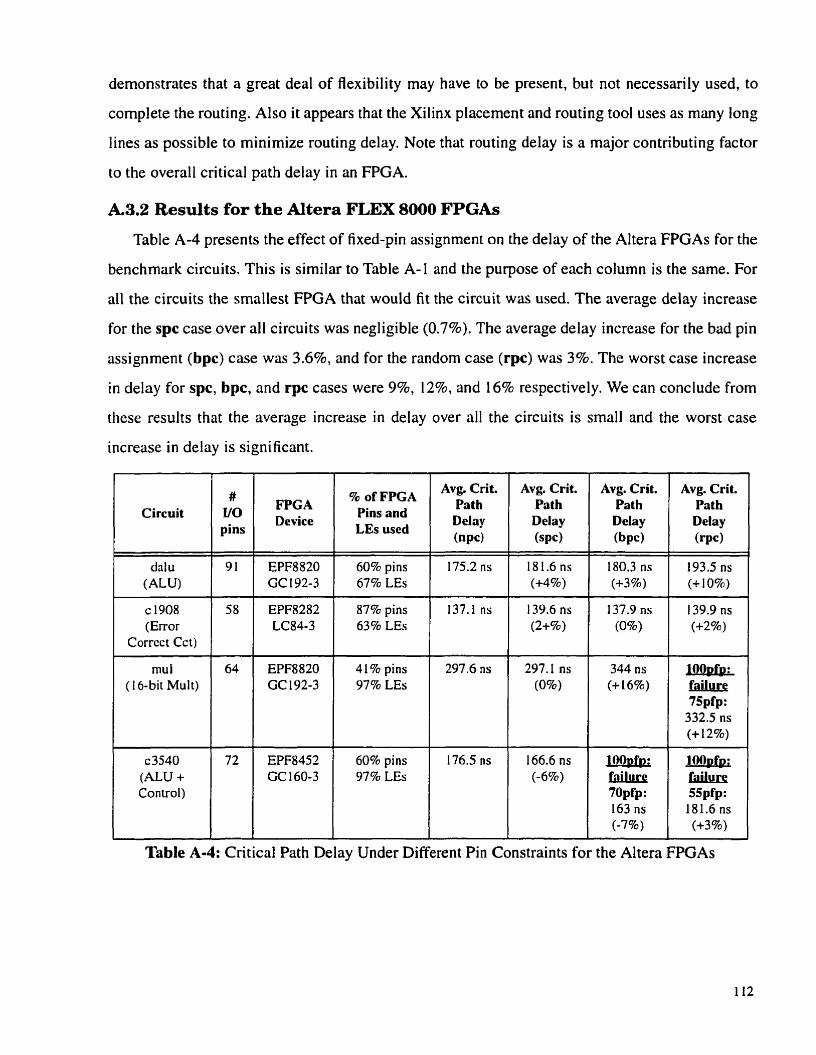
demonstrates that a great deal of Rexibility may have to be present, but not necessarily used, to
complete the routing. Also it appears that the Xilinx placement and routing tool uses as many long
lines as possible to minimize routing delay. Note that routing delay is a major contributing factor
to the overall critical path delay in an FPGA.
A.3.2 Results for the Altera FLEX 8000 FPGAs
Table A-4 presents the effect of fixed-pin assignment on the delay of the Altera FPGAs for the
benchmark circuits. This is similar to Table A-1 and the purpose of each colurnn is the same. For
al1 the circuits the smallest FPGA that would fit the circuit was used. The average delay increase
for the spc case over al1 circuits was negligible (0.7%). The average delay increase for the bad pin
assignment (bpc) case was 3.6%, and for the random case (rpc) was 3%. The worst case increase
in delay for spc, bpc, and rpc cases were 9%, 12%, and 16% respectively. We can conclude frorn
these results that the average increase in delay over al1 the circuits is small and the worst case
increase in delay is significant.
Circuit
d d u W U )
# 'O pins
c 1908 (Error
Corcct Cct)
91
mu l (16-bit Mult)
FPGA Device
58
c3540 (ALU + Control)
. ... --
Avg. Crit. Path Delay (rpc)
Avg. Crit. Pnth Delay (spd
181.6 ns (+4%)
139.6 ns (2+%)
EPF8830 GC 192-3
64
Table A-4: Critical Path Delay Under Different Pin Constraints for the Altera FPGAs
Avg. Crit. Pat h Delay (bpd
180.3 ns (+3%)
137.9 ns (0%)
% of FPGA Pins and LES used
EPF8282 LC84-3
72
Avg. Crit. Path Delay (npc)
60% pins 67% LES
EPF8820 GC 192-3
175.2 ns
87% pins 63% LES
EPF8452 GC 1 60-3
137.1 ns
4 1 % pins 97% LES
297.6 ns
60% pins 97% LES
176.5 ns

Circuit # FPGA
'O Device pins
c 1355 (Error TC 100-3
Correct Cct)
(Error TC 100-3 Correct Cct)
- -
c880 (ALU + Con trol)
S I 196 (Logic)
s 1423 (Logic)
s5378 86 EPF8820 (Logic) GC 192-3
s820 39 EPF8282 (PLW LC84-3
s838 (fractional LC84-3
mult) 8 s9234 1 43 1 EPF8820
(Logic) GC 192-3
Average Increasc
Avg. Crit. Avg. Crit. Avg. Crit. Avg. Crit. % of FPGA Path Pins and Path Path Path
Delay Delay Delay Delay LES used (np4 (spd (bp4 (rp4
95% piris 1 95.4 i i i
95% pins 89.5 ns 39% LES
72% pins 137.5 ns 149.8 ns 144.4 ns 148.9 ns 31% LES (+9%) (+5%) ( 4 % )
43% pins 72.6 ns 70.9 ns 80 ns 75.5 ns 65% LES
37% pins 207.6 ns 203.9ns 207.9 ns 205.6 ns 79% LES (-2%) (0%) (- 1%)
56% pins 66.8 ns 68.6ns 73 ns 71.4 ns 69% LES (+3%) (+9%) (+6%)
60% pins 64 ns 60.1 ns 69.4 ns 62.7 ns 59% LES 1 ( (-6%) 1 (+8%) 1 (-2%)
60% pins 63.1 ns 65.5 ns 67.5 ns 65.1 ns
60% pins 42.5 ns 42.9 n s 41.7 ns 40.3 ns 60% LES (0% (-2%) (-5%)
--
23% pins 1 101.6 ns 1 I p 1 G s 1 1 ~ 0 & $ ~ 1 0 7 . 8 ns 52% LES (+6%)
- - - - -- -- - - - - - -
Table A-4: Critical Path Delay Under Different Pin Constraints for the Altera FPGAs
Two circuits (c3540 and ~1355) were un-routable for the bpc case and three circuits (mul,
c3540, and ~1355) were un-routable for the rpc case. To enable the tool to complete routing, some
of the pins were left unassigned (the tool chose the pin assignment). For example, for the circuit
mu1 under the rpc case, 75pfp implies that the circuit would successfully route if 75% of the pins

were fixed and 25% of the pins were left unassigned.
Interconnect Usage (bpc)
mws, Circuit
Interconnect Usage (rpc)
ÇOWS,
I 1 coiumns 1 columns 1 columns 1 coiumns
Interconnect Usage (npc)
mws,
Interconnect Usage (spc)
rows,
c3540 (ALU +
cl355 (Error
Correct Cct)
t da lu W U )
c 1908 (Error
Corrcct Cct)
3 10 88
138 46
~ 4 9 9 (Error
Correct Cct) - - -- -
c880 (ALU + Control)
304(-2%) 109(+24%)
122(+3%) 43(-7%)
86 55
- -
1 03 60
S I 196 (Logic)
s 1423 (Log ic)
329(+6%) 149(+69%)
1 16(-2%) 44(-4%)
84(-2%) 56(+2%)
140(0%) 39(+22%)
s5378 1 E8 (Logic)
Table A-5: Routing Resource Utilization for the Altera FPGAs
328(+6%) 155(+76%)
1 30(+ 10%) 49(+7%)
1 00(+8 %) 94(+ 1 %) 23(+35%) 1 17(0%)
(fractional mu1 t)
s9234 (Logic)
97(+ 13%) 61(+11%)
1 50(+6%) 76(+ 138%)
1 O 1 (+9%) 16(-6%)
424(+ 14%) 144(+33%)
1 04(+2 1 %) Gl(+ll%)
150(+6%) 76(+138%)
7
260 64
438(+180/0) 174(+6 1 %)
469(+26%) 196(+8 1 %)
9(+29%)
280(+8%) 87(+36%)
1 0(+43 %)
286(+10%) 86(+34%)
1 0(+43 7%)
289(+ 1 1 %) 98(+53%)

Table A-5 gives the routing utilization obtained for the same placement and routing experi-
ments as in Table A-4. This is similar to Table A-2 and the purpose of each column is the same.
Altera uses a two-level hierarchical routing architecture and the routability is determined by the
utilization of the row and column fast track interconnects that span the whole length and width of
the chip [Alte94b]. Compared to the npc case, the average increase in utilization of row and col-
umn fast track interconnect is quite pronounced in al1 other pin constraint cases. For all the cir-
cuits, the worst case increase in utilization of routing tracks due to pin constraints are 36%, and
1 38% respectively for row and column fast track interconnects.
The Altera FLEX 8000 FPGAs seem to be slightly susceptible to routing failures under ran-
dom pin constraints in cases where the V 0 pin or logic element utilization is close to 100%. The
cause of this seems to be the architectural restriction that each UO pin can connect to only one
(unique) row or column of routing tracks (fast tracks). Some flexibility here, e.g. allowing an UO
pin to connect to a number of rows or columns, will probably lead to better routability under ran-
dom pin constraints. It seems that system designers, when implernenting a circuit using FLEX
8000 FPGAs, should leave about 20% of the logic elernents and U 0 pins free to avoid routability
problems due to pin constraints. For Iess tightly packed circuits, the amount of routing resources
used were increased markedly, but there are sufficient routing resources available to handle the
increased demand.
Table A-6 shows the resource utilization statistics for the Altera FPGAs for al1 the benchmark
circuits used. The information in this table is basically the same as that available in Table A-4 and
Table A-5, but it is presented in a manner that shows the percentage of total available FPGA logic
and routing resources used by each circuit. Over al1 the circuits under the npc case, the average
utilization of row and colurnn fast tracks are 48% and 19% respectively. Over al1 the circuits and
Circuit
Average Increase
Table A-5: Routing Resource Utilization for the Altera FPGAs
Faci tTrac k Interconnect Usage (npc)
rows, columns
FastTrack Interconnect Usage (spc)
rows, columns
row tracks:3% col tracks: 14 %
FastTrac k lnterconnect Usage (bpc)
mws, columns
row tracks:7% col tracks:33%
Fast'ïrack Interconnect Usage (rpc)
rows, columns
row tracks: 13 % col tracks:43%

pin constraint cases. the maximum utilization of row and column fast tracks are 86% and 58%.
Circuit
dalu (ALU)
c 1908 (Error
Correct Cct)
mu1 (16-bit Mult)
# 'O pins
FPGA Devire
c3540 (ALU + Control)
c 1355 (Error
Correct Cc t)
c499 (Error
Correct Cct)
91
58
64
s1196 (Logic)
s 1423 (Logic)
s5378 (Logic)
5820 (PLDI
s832 mm
% FPGA Pins and LES used
% of FPGA routing
resources used (bpc) rows,
columns
49% 44%
cg80 86 EPF8453 72% pins 31% 31% (ALU+ 1 1 GCl60-3 1 3I%LEr 1 18% 1 19% Control)
72
73
73
% of FPGA routing
resources used (rpd rows,
cotumns
49% 46%
EPF8820 GC 192-3
EPF8282 LCS 4-3
EPF8820 GC192-3 ,
1
30
24
86
39
39
% of FPGA routing
resourees uscd (npc)
EPF8452 GC 160-3
EPF8282 TC 100-3
EPF8282 TC 100-3
% of FPGA routing
resources used (spc)
60% pins 67% LES
87% pins 63% LES
4 1 % pins 97%LEs ,
Table A-6: Routing Resource Utilization Statistics for the Altera FPGAs I
EPF8452 LC84-3
EPF8282 LC84-3
EPF8820 GC 192-3
EPF8282 LC84-3
EPF8282 LC84-3
60% pins 97% LES
95% pins 39% LES
95% pins 39% LES
rows, columns
46% 26%
66% 22%
65% 35%
I
43% pins 65% LES
37% pins 79% LES
56% pins 69% LES
60% pins 59% LES
60% pins 60% LES
rows, columns
45% 32%
59% 21%
73% 39%
70% 20%
42% 27%
41% 26%
70% 20%
42% 27%
40% 27%
1
42% 10%
45% 8%
55% 32%
41% i 1%
39% 12%
42% 12%
48% 11%
63% 43%
45% 12%
42% 12%
9 I
l

Circuit
s838 (fractionri1
mult)
s9234 (Logic)
Average Utilization
routing %ofFPGA resouires
Pins and LES used
used (npc) FOWS,
columns
60% pins
-
23% pins 52% LES
61% pins 48% 63% LES 19%
% of FPGA routing
m o u mes used (SPC)
rows, columns
% of FPGA routing
resources used (bp4 rows,
columns
% of FPGA routing
resources used (rpc) rows,
columns
Table A-6: Routing Resource Utilization Statistics for the Altera FPGAs
A.4 Conclusions
In this Appendix we presented experimental results on the effects of fixing FPGA pin assign-
ment on the speed and routnbility of FPGAs. We showed that the effects on delay are marginal on
average and significant in particular cases. The effects on delay are more pronounced in the case
of circuits that use up almost al1 of the available FPGA VO pins and Iogic blocks. The effects on
routability are significan t for almost al1 the circuits.
The main contribution of this study is that we have presented some quantitative results on the
effects of fixing FPGA pins on delay and routability. So far the evidence to this effect was mec-
dotal, and contras, to what our results indicate. Our results will be useful to system designers
using FPGAs in their hardware designs and to architects and CAD tool developers involved in the
developrnent of architectures and layout synthesis tools for multi-FPGA systems.
It appears that the extra long lines provided on the periphery of XC4000 FPGAs are effective
in handling pin constraints. One research issue this raises is how many such lines should be pro-
vided for WGAs of different sizes and different number of I/0 pins. Circuits that utilize carry
chains and wide edge decoders [Xili94b] may limit the flexibility available to the placement and
routing tool. The etiect of pin constraints may be more pronounced for such circuits. Also the
effects of pin constraints on performance driven placement and routing of FPGAs needs to be

investigated.

- - -
Appendix B
Experimental Results Showing Actual Pin Cost and Delay Values
In many tables in Chapter 4 and 5, the pin cost and the critical path delay values were given in
a normalized manner. In this Appendix, the tables showing the actual (un-nomalized) pin cost
and critical path delay values are presented, which corresponding to specific tables in Chapter 4
and Chapter 5.
Circuit
~ 3 5 9 3 2
s384 17
s3858 4
mips64
spla
cspla
mrtc64
sort3
firl6
gra I
Table B-1: Critical Path Delays at Different Levels of Circuit Implementation
#FPGAs
8
9
9
14
18
18
6
12
1 O
4
Critical path delay (in ns)
Pre-partitioning, CPD
34
44
71
230
3 8
36
260
1 45
96
54
Post-partitioning, CPD-PP
37
59
94
3 15
86
82
38 1
304
134
57
Post-routing, CPD-PR
5 7
94
139
462
196
193
623
533
238
70

Circuit
fpsdes
spsdes
ochip64
ralu32
iir 16
Average
Table B-2: Cornparison of HROUTE and HROUTE-TD
Circuit
~35932
s384 17
~38584
mips64
spi ri
çsplri
mac64
sort8
firl6
gra
fpsdes
s psdes
oc hip64
rai u32
iirl6
Average
Table B-1: Critical Path Delays at Different Levels of Circuit Implementation
#FPGAs
9
8
8
9
6
10
#FPGAs
8
9
9
14
18
18
6
12
1 O
4
9
8
8
9
6
10
Critical path delay (in ns)
Post-routing critical path delay, CPD-PR
Post-routing, CPD-PR
227
249
63
3 17
1 60
241
Pre-partitioning, CPD
96
138
22
92
129
99
(in
HROUTE
57
95
113
468
204
191
563
538
193
59
195
2 16
50
298
152
226
Posbpartitioning, CPD-PP
136
172
29
157
135
145
ns)
HROUTE-TD
53
94
98
418
169
1 64
465
499
1 67
57
176
205
50
263
152
202

Postrouting critical path delay ushg PCROUTE (in ns)
Circuit # FPGAs I I I
Table B-3: The Effect of Pp on the Delay of the Partial Crossbar Architecture
Post-routing critical path delay using FPSROUTE (in ns)
~35932
s384 17
~38584
mips64
spla
cspla
rnric64
sort8
fir 16
I r a
fpsdes
s psdes
ochip64
rdu32
iirl6
8
9
9
14
18
18
6
12
10
4
9
8
8
9
6
Average
I L
Pt =47
57
94
139
462
196
193
623
533
238
70
227
249
63
3 17
160
24 1
Pt = 47
57
94
139
462
27 1
23 8
623
588
23 8
70
227
249
6 3
317
160
253
Pt = 17
57
94
139
462
196
193
623
533
238
70
227
249
63
317
160
241
Pt = 17
82
120
1 64
463
287
238
623
608
244
70
227
249
63
3 30
160
262
Pt = 4
57
94
139
462
196
193
623
533
238
70
227
249
63
317
160
24 1
P, = 4
82
1 20
164
50 I
3 17
262
623
652
244
70
280
274
6 3
Rou ting failure
160
281

I 1 Nurnber of FPGAs I Pin cost
1 Circuit 1 1 I 1 1
Partial Partial 1 cmssbar 1 HCCP / cmssbnr 1 HCGP
gra 4 4 1516 1216
fpsdcs 9 9 341 1 2736
Post-routing critical path delay (in ns)
Partiai 1 HCCP 1 cross bar
spsdcs 8 8 3032 2432
oc hip64 8 8 3032 2432
d u 3 2 9 14 341 1 4256
iir 16 6 6 2274 1824
Avg.: 10 Avg.: 10 Total: Total: 56092 47424
Avg.: 241 Avg.: 202 I I Table B-4: Cornparison of the HCGP and Partial Crossbar Architectures
Comment Observe from this table that the estimated clock speeds for the partial crossbar architecture
range from 20 MHz for the ochip64 circuit to 2 MHz the sort8 circuit. This range is representative
of the clock rates expected in MFSs for rapid prototyping and logic emulation [Quic98]. This is a
validation of our layout synthesis tools and the timing mode1 used in O u r timing analysis tool
(MTA).

Table B-5: Cornparison of the HTP and HCGP Architectures
Circuit
~35932
s384 17
~38584
mips64
splri
cspfa
mac64
sort8
fi^-16
Ers
fpsdes
spsdcs
ochip64
raIu32
iirl6
Number of FPGAs
HTP
9
9
9
16
30
25
8
14
12
4
9
8
8
16
6
Avg.: 12
HCCP
8
9
9
15
18
18
6
14
1 O
4
9
8
8
14
6
Avg.: 10
- - - -
Pin cost
HTP
2736
2736
2736
4864
9520
7600
2432
-
Post-routing critical path delay (in ns)
HCGP
243 2
273 6
273 6
4560
5472
5472
1824
4256
3648
1216
2736
2432
2432
4864
1824
Total: 56032
HTP
5 3
88
113
303
232
205
529
HCGP
53
94
98
4 18
169
1 64
465
4256 1 535 1 499
3040
1216
2736
2432
2432
4256
1824
Toîal: 47424
197
60
199
232
6 3
325
152
Avg.: 226
167
57
176
205
50
263
152
Avg.: 202

Number of FPGAs Pin cost Post-routing critical path delay (in ns)
-- - - - pp - - - - -
Table B-6: Cornparison of the HWCP and HCGP Architectures
Circuit
~35932
s384 I7
~38584
mips64
spla
CS pla
mric64
sort8
tir16
fpsdes
spsdes
ochip64
raIu32
iirl6
HWCP (Cs = 4)
8
12
12
16
20
20
8
16
12
4
12
8
8
16
8
Avg.: 12
HCGP
8
9
9
15
18
18
6
14
10
4
9
8
8
14
6
Avg.: 10
HWCP (Cs = 4)
2432
3648
3648
4864
5472
5472
2432
4864
3648
1216
3648
2432
2432
4256
2432
Total: > 54720
HWCP (Cs =4)
57
111
118
4 14
routing failurc
routing failurc
533
573
199
57
227
235
G3
routing faiiure
169
Avg. 229
HCGP
2432
2736
2736
4560
5472
5472
1824
4256
3040
1216
2736
2432
2432
4256
1824
Total: 47424
HCGP
53
94
98
418
169
1 64
465
499
167
57
176
205
50
263
152
Avg.: 202

References [Alte941
[Al te94a]
[AIte94b]
[Apti98]
[Apti93]
[Amer951
[Arno921
[Babb93]
(Babb971
[Baue98]
Dehr961
[Bert931
Altera Corporation, Recoizfigrtrubk lnterconnect Peripheral Processor
(RIPPI O) Users Manual, Version 1 .O, 1994.
Altera Corporation, MAX+PLUS II User Mnnual, 1994.
Altera Corporation, FLEX 8000 Handbook, 1994.
Aptix Corporation, Product brief: The S ystem Explorer MP4, 1 998. Available
on Aptix Web site: http://www.aptix.com.
Aptix Corporation, Data Book Srtpplemerit, San Jose, CA, September 1993.
R. Amerson et al, "Teramac -- Configurable Custom Computing," Proceedings
of IEEE Syinposirtrn on FPGAs for Ciistom Cornpuling Mnclzines, pp. 32-3 8,
1995.
J. M. Arnold, D. A. BueIl, and E. G. Davis, "Splash 2," Proceedings of 4th
Anmial ACM Symposium on Pimllel A lgonthms and Architectures, pp. 3 1 6-
322, 1992.
J. Babb et al, "Virtual Wires: Overcorning Pin Limitations in FPGA-based
Logic Emulators," Proceedings of IEEE Workshop on FPGAs for Cttsrorn
Computing Mucizines, pp. 142- 1 5 1 , 1993.
J. Babb et al, "Logic Emulation with Virnial Wires," lEEE Trans. on CAD, vol.
16, no. 6. pp. 609-626, June 1997.
J. Bauer et al, "A Reconfigurable Logic Machine for Fast Event-Driven Simu-
lation," Procof the Design Automation Conference, pp. 668-67 1, 1998.
D. Behrens, K. Harbich, and E. Barke, "Hierarchical Partitioning", Proc. of
Iritemational Conference on CAD (ICCAD'96), pp. 470-477, 1996.
P. Bertin, D. Roncin, and J. Vuillemin, "Programmable Active Mernories: A
Performance Assessment," Proceedings of the 1993 Symposium: Reseorch on
Integrated Systenis, MIT Press, 1 993.

V. Betz and J. Rose. "VPR: A New Packing, Placement and Routing Tool for
FPGA Research," Proc. of the 7th International Workslzop on Field-Program-
inable Logic, London, pp. 2 13-222, August 1997.
S. Brown, R. Francis, J. Rose, and Z. Vi-anesic, Field Prognlrnrnable Gate
Arrays, Kluwer Academic Publishers, 1992.
M. Butts, J. Batcheller, and I. Varghese, "An Efficient Logic Emulation Sys-
tem," Proceedings of iEEE International Cor$erence on Cornputer Design, pp.
138-141, 1992.
M. Butts, "Future Directions of Dynamically Reprogrammable Systerns,,'
Proc. of IEEE C~cstoin Integrated Circriits Coirfrrence, pp. 487-494, 1995.
S. Casselman, "Virtual Computing and The Virtual Cornputer," Proceeciings of
IEEE Workshop on FPGAs for C~rstom Cornpiiti~ig Machines. pp. 43-48, 1993.
P. K. Chan, M. D. F. Schlag, "Architectural Trade-offs in Field-Programmable-
Device-Based Computing Systems," Proceedings of IEEE Worksliop on
FPGAs for Custorn Compiiiing Machines, pp. 1 52- 16 1, 1993.
[Chan93a] P. K. Chan, M. D. F. Schlag, and J. Y. Zen, "On Routability Prediction for
FPGAs," Proceedirzgs of 30th ACMnEEE DAC, 1993.
[Chan93 b] P.K. Chan, University of California, Santa Cruz, California, Privcite Cornmuni-
ccr tion .
P. K . Chan, M. D. F. Schlag and J. Y. Zien, "Spectral-Based Multi-Way FPGA
Partitioning:' International Symposium on Field-Programinable Gate Arrays,
pp. 133-139, 1995.
L. L. Chang, "Static Timing Analysis of High-Speed Boards," IEEE Spectrum,
vol. 34, no. 3, March 1997.
N. Chou et al, "Local Ratio Cut and Set Covering Partitioning for Huge Logic
Emulation Systems," iEEE Trans. on CAD, vol. 14, no. 9, pp. 1085-1092, Sep-
ternber 1995.
K. C. Chu, Quickturn Design Systems, San Jose, California, Private Commrrni-

cation.
C . Clos, "A Study of Non-Blocking Switching Networks," The Bell System
Technical Journal, vol. XXXII, pp. 406-424, March 1953.
M. Courtoy (Aptix Corp.), "Prototyping Engines: How Efficient and Practi-
cal?," Invited Talk, Sixth IFIP International Workshop on Logic and Arckitec-
trrre Syntlzesis (IWLASP97), 1 997.
J. Darnauer et al, "A Field Programmable Multi-chip Module (FPMCM)," Pro-
ceedings of IEEE Symposirtm on FPGAs for Cusront Computing Machiries, pp.
1-9, 1995.
1. Dobbelaere et al, "Field Programmable MCM Systerns -- Design of an Inter-
connection Früme," IEEE Otstom Integraiecl Circuits Conference, pp. 4.6.1 -
4.6.4, 1992.
T. H. Drayer, W. E. King, I. G. Tront, and R. W. Conners, "MORKPH: A Mod-
ular and Reprogrammable Real-tirne Processing Hardware," Proceediings of
IEEE Syrnposiron on FPGAs for Custotn Computing Machines, pp. 1 1 - 19,
1995.
S. S. Erdogan and A. Wahab, "Design of RM-nc: A Reconfigurable Neurocom-
puter for Massively Parallel-Pipelined Computations," Iizternational Joint
Coiflerence on Nertrnl Nehvorks, Vol. 2, pp. 33-38, 1992.
Exemplar Logic, VHDL Synthesis Refereizce Manual, 1994.
W. Fang and A. Wu, "Performance-Driven Multi-FPGA Partitioning Using
Functional Clustering and Replication," Proc.of the Design Automation Con-
ference, pp. 94-99, 1998.
C. M. Fiduccia, and R. M. Mattheyses, "A Linear-Time Heuristic for Improved
Network Partitions", Proc. of 19th ACMLEEE Design Automation Conference,
pp. 24 1-247, 1982.
Proceedings of IEEE WorkFhops/Symposia on FPGAs for Custorn Cornpuring
Machines, 1992 to 1996.

D. Galloway, D. Karchmer, P. Chow, D. Lewis, and J. Rose, "The Transmogri-
fier: The University of Toronto Field-Programmable System", CSRI Technical
Report (CSRI-306), CSRI, University of Toronto, 1994.
D. Galloway, "The Transmogrifier C Hardware Description Language and
Compiler for FPGAs," Proceedirtgs of IEEE Symposium on FPGAs for Custom
Compiting Machines, pp. 136- 144, 1995.
G. Ganapathy et al, "Hardware Emulation for Functional Verification of K5,"
Procof the Design Automation Conference, pp. 3 15-3 18, 1996.
J. Gateley et al, " U ~ ~ ~ ~ S P A R C ~ ~ - I Emulation ," Proc.of the Design Automntioit
Coilference, pp. 13- 18, 1995.
M. Gokhale et al, "Building and Using a Highly Parallel Programmable Logic
Array," IEEE Computer, pp 8 1-89, January 199 1 .
S. Goto, "An Efficient Algorithm for the Two-Dimensional Placement Problem
in Electric Circuit Layout," IEEE Traits. on Circuits and Systerns, Vol. 28, No.
1, pp. 12- 18, January 198 1 .
R. Guo et al, "A 1024 Pin Universal Interconnect Array with Routing Architec-
ture," Proc. of IEEE Custum Integrczted Circiiits Con ference, pp. 4.5.1 -4.5.4,
1992.
S. Hauck, G. Boriello, C. Ebeling, "Mesh Routing Topologies for Multi-FPGA
Systems", Proceedings of Interncitional Conference on Compriter Design
(ICCD'941, pp. 170-177, 1994.
[Hauc94b] S. Hauck and G. Boriello, "Pin Assignment for Multi-FPGA systems", Pro-
ceedings of IEEE Workshop on FPGAs for C~tstorn Compriting Machines,
1994.
[Hauc95] S . Hauck, Multi-FPGA S ystems, Ph.D. Thcsis, University of Washington,
Department of Computer Science and Engineering, 1995.
[Hauc98a] S. Hauck, "The Roles of FPGAs in Reprogrammable Systems", Proceedings of
the IEEE, vol. 86, no. 4, pp. 615-638, July 1998.

[Haucgdb] S. Hauck and A. Agarwal, "Software Technologies for Reconfigurable Sys-
[He i 1971
[Hoel941
[Hu tt963
[Icub97]
[Icu b94]
[Ikos98]
[Joup87]
[Karc94]
[Kha195]
[Kha197]
[Kha198]
tems", subrnitted to IEEE Tram. on Cornpurers, 1998.
F. Heile, Altera Corporation, San Jose, California, Privnte Communication.
W. Hoel ich, Aptix Corporation, San Jose, Cali fomia, Private Cornminication.
M. Hutton, J.P. Grossman, J. Rose and D. Corneil, "Characterization and
Parameterized Random Generation of Digital Circuits," Procof the Design
Autontution Conference, pp. 94-99, 1996.
1-Cube, Inc., The IQX Fnmiiy Daru Sheet, May 1997. Available at:
www.icube.com.
1-Cube, Inc., "Using FPID Devices in FPGA-based Prototyping," Application
note, Part nrmbecD-22-002, February 1994.
IKOS Systems, Product Brief: VirtuaLogic-8 Emulation System, Available at
www.ikos.com.
Norman P. Jouppi, "Timing Analysis and Performance Improvement of MOS
VLSI Designs," IEEE Truns. on CAD, vol. CAD-6, no. 4, pp. 650-665, July
1987.
D. Karchmer, A Field-Programmable System with Reconfigurable Memory,
M.A.Sc. Thesis, Dept. of Electrical and Cornputer Engineering, University of
Toronto, 1994.
M. A. S. Khalid and J. Rose, "The Effect of Fixed VO Pin Positioning on The
Routability and Speed of FPGAs," Proceedings of The Third Canadian Work-
shop on Field-Programnrnble Devices (FPD '95), pp. 92- 104, 1995.
M. A. S. Khalid and J. Rose, "Experimental Evaluation of Mesh and Partial
Crossbar Routing Architectures for Multi-FPGA Systems," Proceedings of the
Sixth IFIP International Workshop on Logic and Architecture Synthesis
(IWLAS '97), 1997.
M. A. S. Khalid and J. Rose, "A Hybrid Complete-Graph Partial-Crossbar
Routing Architecture for Multi-FPGA Systems," Proc. of 1998 Sixth ACM

International Symposium on Field-Programmable Gate Arrays (FPGA198), pp.
45-54, February 1998.
[Kim961 C. Kim, H. Shin, "A Perforrnance-Driven Logic Emulation System: FPGA
Network Design and Perfomance-Driven Partitioning," IEEE Trans. or2 CAD,
vol. 15, no. 5, pp. 560-568, May 1996.
[Knap96] D. W. Knapp, Behavioral Synthesis: Digital System Design Using the Syriopsys
Behavioral Compiler, Prentice Hall PTR, 1996.
[Kris84] B. Krishnamurthy, "An Improved Min-Cut Algorithm for Partitioniog VLSI
Networks," lEEE Trans. on Compcïfers, vol. C-33, no. 5, pp. 438-446, May
1984.
[Kuh86] E. S. Kuh and M. Marek-Sadowska, "Global Routing," in Layout Design und
Verifcation, Edited by T. Ohtsuki, North-Holland, pp. 169- 198, 1986.
[Kun1931 R. Kuznar et al, "Partitioning Digital Circuits for Implementation on Multiple
FPGA ICs," MCNC Technical Report 93-03, North Carolina, 1993.
[Kuzn94] R. Kuznar et al, "Multi-way Netlist Partitioning into Heterogeneous FPGAs
and Minimization of Total Device Cost and Interconnect," frocof the Design
Autotnntion Conference, pp. 238-243, 1994.
[Lang41 S. Lm, A. Ziv and A. EI-Gamal, "Placement and Routing for A Field Program-
mable Multi-Chip Module," Proc.of the Design A~rtornarion Conference, pp.
295-300, 1994.
[Lang51 S. Lm, Architecture and Cornputer Aided Design Tools for a Field Program-
mable Multi-chip Module, Ph. D. Thesis, S tanford University, 1995.
[Lee611 C. Lee, "An Algorithm for Path Connection and its Applications," IRE Truns.
on Electronic Cornputers, vol. EC-IO, no. 3, pp. 346-365, 196 1.
[Lewi93] D. M. Lewis, M. Van Ierssel, and D. H. Wong, "A Field Programmable Accel-
erator for Compiled Code Applications," Proceedings of IEEE Workshop on
FPGAs for Otsrom Compriting Machines, pp. 60-67, 1993.
[Lewi97] D. M. Lewis, D. R. Galloway, M. Van Ierssel, J. Rose, and P. Chow, "The

[Lew i98]
[Lin971
f Mak95aI
[Mak95b]
Transmogrifier-2: A 1 Million Gate Rapid Prototyping System," Proceedings
of FPGA '97, pp. 53-6 1, 1997.
D. M. Lewis, D. R. Galloway, M. Van Ierssel, J. Rose, and P. Chow, "The
Transmogrifier-2: A 1 Million Gate Rapid Prototyping System," IEEE Trans.
on VLSI Systems, vol. 6, no. 2, pp. 188- 198, June 1998.
S. Lin, Y. Lin, and T. Hwang, "Net Assignment for the FPGA-Based Logic
Emuiation System in the Folded-Clos Network Structure," IEEE Trans. on
CAD, vol. 16, no. 3, pp. 316-320, March 1997.
Wai-Kei Mak, D. F. Wong, "On Optimal Board-Level Routing for FPGA-based
Logic Ernulation," Proc. of 32nd Design Automation Conference, pp. 552-556,
1995.
Wai-Kei Mak, D. F. Wong, "Board-Level Multi-Terminal Net Routing for
FPGA-based Logic Emulation," Proc. of Intentational Conference on C'AD
(ICCAD '95), pp. 339-344, 1995.
[McMugS] L. McMurchie and Car1 Ebeling, "PathFinder: A Negotiation-Based Perfor-
(Mon tg81
[Page9 1 ]
[Prep96]
[Quic94]
[Quic98]
mance-Driven Router for FPGAs," Proc. of 1995 Third ACM International
Syniposiur?i on Field- Progra~rintnble Gate A rruys (FPGA '95), pp. 1 1 1 - 1 1 7,
1 995.
S. Montazeri, AT1 Technologies Inc., Unionville, Ontario, Privute Comrnuni-
catiorz, 1998.
1. Page and W. Luk. "Compiling Occam into FPGAs," in W. Moore, W. Luk,
Eds., FPGAs, Abingdon EE&CS Books, England, pp. 27 1-283, 199 1.
Programmable Electronics Performance Corporation, HDL models for differ-
ent circuits (synthesis benchmarks) are available on their Web site: http//
w w w.prep.org.
Quicktum Systems, Product brief: The Enterprise Emulation System and Logic
Animator, 1994.
Quickturn Design Systems, Inc., System Realizer product brief, 1998. Avail-
able on Quickturn Web site:http:f/www.quickturn.com.

[Quin79]
[Roy951
[Sm961
[Selv95]
[Sher95]
[S hah9 1 ]
[S hih931
[S Km941
[Syno97]
[Ter1951
[Tess97]
[Tri m94]
N. R. Quinn, M. A. Breuer, "A Force Directed Component Placement Proce-
dure for Printed Circuit Boards," IEEE Trans. on Circuits and Systems, Vol. 26,
No. 6, pp. 377-388, June 1979.
K. Roy-Neogi and C. Sechen, "Multiple-FPGA Partitioning with Performance
Optimization," Ir~ternationnl Svmposinim on Field-Programn~able Gate Arravs,
pp. 146- 152, 1995.
M. Sarrafzadeh and C. K. Wong, An Introdriction to VLSI Physical Design,
McGraw Hill, 1996.
C. Selvidge et al, "TIERS: Topology Independent Pipelined Routing and
Scheduling for Vinual Wire Compi Mon," Proceedings of FPGA '95, pp. 25-
31, 1995.
N. S herwani, Algorithnrs for VLSl Plzysicnl Design Automntion, Kluwer Aca-
demic Publishers, 1995.
K. Shahookar and P. Mazurnder, "VLSI Ce11 Placement Techniques,'' ACM
Corripuring Birvqs, Vol. 23, No. 2, pp. 143-220, June 199 1.
M. Shih, E. S. Kuh, "Performance-Driven Systern Partitioning on Multi-Chip
Modules," froc. of the Design Aiitomation Corference, pp. 53-56, 1992.
M. Slimane-Kadi, D. Brasen, and G. Saucier, "A Fast-FPGA Prototyping Sys-
tem That Uses Inexpensive High Performance FPIC," Internatiorznl Workshop
on Field Programnznble Gate Arrays, 1994.
Synopsys, Inc., Design Compiler(Version 3.44, Behavioral Compiler (Version
3.4a), and Library Compiler (Version 3.4a), Refrrence Manuals. Documents
available on-line.
R. Terril, "A 50000-gate MCM-based PLD for Gate Amy Prototyping," IEEE
Cicstom Integrated Circuits Conference, pp. 2.2.1-2.2.4, 1995.
R. Tessier, MIT Laboratory for Computer Science, Cambridge, MA, Privote
Conrmunicntion, 1997.
S. M. Trimberger, Field Programmable Gate Array Technology, Kluwer Aca-

[Trim95]
[Van921
[Varg93]
[Vui 1961
[WaI t9 1 ]
[ W O O ~ ~ ]
[Xili94a]
[Xili94b]
[Xili97]
[Yang9 11
demic Publishers, 1994.
S. M. Trimberger, Xilinx Inc., San Jose, California, Private Communication.
D. E. Van Den Bout, et al, "Anyboard: An FPGA-Based Reconfigurable Sys-
tem," IEEE Design and Test of Computers, pp. 2 1-30, June 1992.
J. Vargese, M. Butts, and Jon Batcheller, "An Efficient Logic Emulation Sys-
tem", IEEE Trans. on VLSI Systems, vol. i, iio. 2, pp. 17 1 - 174, June 1993.
J. E. Vuillemin, P. Bertin, D. Roncin, M. Shand, H. Touati, and P. Boucard,
"Programmable Active Memories: Reconfigurable Systems Corne of Age,"
IEEE Transactions on VLSI, Vol 4, No. I , pp. 56-69, March 1996.
S. Walters, "Cornputer-Aided Prototyping for ASIC-Based Systerns," lEEE
Design c d Tesr of Computers, pp. 4- 10, June 1992.
N. Woo and J. Kim, "An Efficient Method of Partitioning Circuits for Multi-
FPGA Implementation," Proc. of 30th Design Autorriation Conference, pp.
202-307, 1 993.
Xilinx, Inc., XACT Development Systern User Giiide, February 1994.
Xilinx, Inc., The Programmable Logic Data Book (page 9- 1 l), 1994.
Xilinx, Inc., Product Specification: XC4000E and XC4000X Series FPGAs,
Version 1.2, June 16, 1997. Available on Xilinx Web site: www.xilinx.com.
S. Yang, Logic Sy~ithesis arid Opriniization Be~ichrnarks User Guide, Vers ion
3 .O, Microelectronics Center of North Carolina, January 1 99 1 .