warwick.ac.uk/lib-publicationswrap.warwick.ac.uk/74523/1/wrap_tpel-reg-2014-05-0717.r2.pdf · bjt...
TRANSCRIPT

warwick.ac.uk/lib-publications
Original citation: Bonyadi, Roozbeh, Alatise, Olayiwola M., Jahdi, Saeed, Hu, Ji, Ortiz Gonzalez, Jose, Ran, Li and Mawby, P. A. (2015) Compact electrothermal reliability modeling and experimental characterization of bipolar latchup in SiC and CoolMOS power MOSFETs. IEEE Transactions on Power Electronics, 30 (12). pp. 6978-6992. Permanent WRAP URL: http://wrap.warwick.ac.uk/74523 Copyright and reuse: The Warwick Research Archive Portal (WRAP) makes this work by researchers of the University of Warwick available open access under the following conditions. Copyright © and all moral rights to the version of the paper presented here belong to the individual author(s) and/or other copyright owners. To the extent reasonable and practicable the material made available in WRAP has been checked for eligibility before being made available. Copies of full items can be used for personal research or study, educational, or not-for profit purposes without prior permission or charge. Provided that the authors, title and full bibliographic details are credited, a hyperlink and/or URL is given for the original metadata page and the content is not changed in any way. Publisher’s statement: “© 2015 IEEE. Personal use of this material is permitted. Permission from IEEE must be obtained for all other uses, in any current or future media, including reprinting /republishing this material for advertising or promotional purposes, creating new collective works, for resale or redistribution to servers or lists, or reuse of any copyrighted component of this work in other works.” A note on versions: The version presented here may differ from the published version or, version of record, if you wish to cite this item you are advised to consult the publisher’s version. Please see the ‘permanent WRAP URL’ above for details on accessing the published version and note that access may require a subscription. For more information, please contact the WRAP Team at: [email protected]
IEEE TRANSACTIONS ON POWER ELECTRONICS, TPEL-Reg-2014-05-0717.R2
1
Abstract— In this paper, a compact dynamic and fully-coupled
electro-thermal model for parasitic BJT latch-up is presented and
validated by measurements. The model can be used to enhance the
reliability of the latest generation of commercially available
power devices. BJT latch-up can be triggered by body-diode
reverse-recovery, hard commutation with high dV/dt or from
avalanche conduction during unclamped-inductive-switching. In
the case of body-diode reverse-recovery, the base current that
initiates BJT latch-up is calculated from the solution of the
ambipolar diffusion equation describing the minority carrier
distribution in the anti-parallel PiN body-diode. For hard
commutation with high dV/dt, the displacement current of the
drain-body charging capacitance is critical for BJT latch-up
whereas for avalanche conduction, the base current is calculated
from impact ionization. The parasitic BJT is implemented in
Simulink using the Ebers-Moll model and the temperature is
calculated using a thermal network matched to the transient
thermal impedance characteristic of the devices. This model has
been applied to CoolMOS and SiC MOSFETs. Measurements
show that the model correctly predicts BJT latch-up during
reverse-recovery as a function of forward-current density and
temperature. The model presented, when calibrated correctly by
device manufacturers and applications engineers, is capable of
bench-marking the robustness of power-MOSFETs.
Index Terms— Body Diode, Compact Electro-thermal
Modelling, Inverter, MOSFET, PiN Diodes, Parasitic BJT
Latch-up, SiC MOSFET Reliability.
I. INTRODUCTION
ODY-DIODES can sometimes be used as the anti-parallel
diodes in power MOSFET circuits. Because of the voltage
Manuscript received May 13, 2014, Revised August 18. 2014 and October
27, 2014; accepted December 20, 2014. Date of publication January 4, 2015.
This work was supported by EPSRC funding in collaboration with Jaguar
Land Rover Automotive PLC and EPSRC funding through the underpinning
power electronics devices theme research project (EP/L007010/1) and the
components theme research project (EP/K034804/1).
The authors are with the School of Engineering, University of Warwick,
Coventry CV4 7AL, UK. (e-mail: [email protected];
[email protected], [email protected], [email protected],
[email protected], [email protected],
Color versions of one or more of the figures in this paper are available
online at http://ieeexplore.ieee.org.
Digital Object Identifier
blocking drift layer between the p-body and the drain, the body
diode is effectively a PiN diode. Power MOSFET body diodes
can be used in applications such as DC-DC buck converters,
bridge topology switching circuits, high performance PV
converter cell and can also be employed in synchronous
rectified brushless DC motor drive inverter circuits [1-6]. In
such applications, diode snappiness and high reverse recovery
charge of the body diode can impose a significant amount of
electrical stress and power loss on the MOSFETs [7]. The
large reverse recovery charge is the result of an excessive
amount of carriers stored in the charge storage region (drift
layer) of the diode. Conventional lifetime control techniques
(gold or platinum doping as well as irradiation) are not
applicable in reducing the carrier lifetime as is the case with
discrete diodes, hence the body diode of the MOSFET can
suffer from significant reverse charge. One of the main
concerns regarding the usage of the body diode of power
MOSFETs is the robustness of the device under hard
commutation; e.g. in synchronous rectification, or in other
circuits such as motor drives or primary side switching of
switch mode power supplies [8, 9].
The high demand for high frequency and efficient power
converters has triggered research into SiC devices including
power MOSFETs [10]. SiC MOSFETs are more suitable for
high voltage and high speed applications due to their higher
breakdown voltage, lower on state resistance and faster
switching. SiC has a significantly smaller minority carrier
lifetime and as a result of the higher critical field, the thickness
of the voltage blocking drift layer is approximately 10 times
less than silicon devices. Consequently, they show smaller
reverse recovery with a higher breakdown voltage. The effect
of using SiC MOSFET in synchronous rectification was
studied in [2] which shows that the reverse recovery of SiC
body diode was negligible as well as an improvement in the
switching speed of the MOSFET. MOSFETs have parasitic
NPN BJTs that can latch-up under the right conditions i.e.
when the emitter-base voltage is forward biased, the base-
collector voltage is reverse biased and there is sufficient body
current in the base [11, 12]. For the BJTs to latch, there must
be a body current sufficient to cause a voltage drop greater
than the emitter base junction voltage of the parasitic BJT. To
prevent this from happening, the source is usually grounded to
Compact Electro-Thermal Reliability Modelling and
Experimental Characterisation of Bipolar Latch-up
in SiC and CoolMOS Power MOSFETs
R. Bonyadi, Student Member, IEEE, O. Alatise, S. Jahdi, Student Member, IEEE, J. Hu, J. A. Ortiz-Gonzalez, L.
Ran, Senior Member, IEEE, P. A. Mawby, Senior Member IEEE.
B
IEEE TRANSACTIONS ON POWER ELECTRONICS, TPEL-Reg-2014-05-0717.R2
2
the body by a high dose body implant and a common metal
contact. However, at high temperatures a non-zero body
resistance and a non-zero body current can cause BJT latch-
up. The high dV/dt of the body diode during reverse recovery
coupled with the parasitic drain-to-body capacitance within the
MOSFET can cause a body current (CdV/dt) sufficient to latch
the parasitic BJT. This is particularly pertinent to SiC
MOSFETs where dV/dt is high, minority carrier lifetime is low
and the body diode is snappy.
CoolMOS devices use the principle of the super-junction to
achieve high blocking voltages while delivering low
conduction losses. The alternate n and p columns in the drift
region means that the body diode is not a conventional PiN
diode and will therefore exhibit a different reverse recovery
characteristic. In this paper, the reliability of the SiC MOSFET
and CoolMOS body diode under reverse recovery is
investigated experimentally and by modelling. The body diode
of the MOSFET has been modelled using the Fourier series
solution to the ambipolar diffusion equation (ADE). This is
coupled with electro-thermal model of the parasitic BJT and is
used as a compact physics-based electro-thermal model for a
SiC MOSFET and Si-based CoolMOS device. The impact of
the temperature as well as current density on the diode
recovery characteristics and failure mechanism of the
MOSFET is investigated by the model and compared with
experimental measurements. The proposed model can be used
to investigate the conditions of device failure during
purposeful or inadvertent reverse recovery of device body
diode. The model is useful for estimating the reliability
performance and giving deeper physical insight to the nature
of bipolar latch-up. Section II describes the development of
the Fourier series model for the body diode, section III
describes the BJT electro-thermal model, and section IV
discusses the results while section V concludes the paper.
II. BODY DIODE MODEL DEVELOPMENT
There have been several publications that have detailed how
the minority carrier distribution profile in the drift region can
be modelled using the Fourier series solution to the ambipolar
diffusion equation (ADE) [9, 13-24]. The reverse recovery
characteristics of the PiN body diode in this paper have been
modelled using the same techniques developed for discrete
PiN diodes. The ADE can also be solved using the finite
difference and finite volume techniques however, the Fourier
series is the most computationally inexpensive way of solving
it without too much loss of accuracy. The model takes
conductivity modulation, Shockley-Read-Hall recombination,
Auger recombination, carrier-carrier scattering, drift, diffusion
and displacement currents, depletion layers behaviour and
local lifetime into account. Moreover, the model calculates the
drift region voltage drop based on the conductivity modulation
in the drift region. The ADE models the concentration of
carriers in the drift region which determines the behaviour of
the device during the reverse recovery and is reconstructed
using Fourier series in one dimension [19, 20]. In case of the
CoolMOS model, it has been assumed that there is negligible
carrier concentration gradient or electric field gradient across
the lateral cross-section of the device in comparison to the
vertical cross-section of the device. As a result, electrons flow
from the cathode (the drain of the MOSFET) into the drift
regions and holes flow from the anode (the p-body of the
MOSFET) into the drift regions. Based on this, the 1-D
solution of the Fourier series is applicable because of the
assumption that the vertical concentration gradients are much
higher than the lateral concentration gradients.
The model has been developed for a discrete PiN diode
initially and in this paper, has been extended to body-diodes
for SiC MOSFETs and CoolMOS devices.
Conductivity modulation in the drift region is the
mechanism through which low conduction losses are enabled
in PiN diodes and depends on minority carrier injection into
the drift region. If the number of injected holes to the drift
region becomes much greater than the background doping of
the drift region, charge neutrality requires that the
concentration of electrons and holes be equal to each other in
that region: p(x)=n(x). Using the continuity equations for the
intrinsic region we have:
nExx
nD
n
t
nnn
HL
2
2 (1)
pExx
pD
p
t
ppp
HL
2
2 (2)
where, τHL is the high level lifetime in the drift region (in
order of 1µs for silicon devices and 0.1 ns for SiC) and Dn (for
Silicon 36.1798 cm2/s and 34.3708 cm2/s for SiC at room
temperature) and Dp (11.6292 cm2/s for Silicon and 2.3258
cm2/s for SiC at room temperature) are the diffusion
coefficients for electron and holes respectively. Diffusion
coefficients in SiC is smaller in comparison with silicon. Using
charge neutrality equation and the continuity equations, ADE
is:
2
2 ),(2),(),(
x
txpVtxp
t
txp
pn
Tpn
HL
(3)
Diffusivity in ADE is calculated using Einstein relationship
(n
q
kTD where k is Boltzmann constant 1.38×10⁻²³ JK-1 and
q is electron charge 1.602×10⁻¹⁹ C) as below:
pn
pn
pn
Tpn
DD
DDVD
22
(4)
The Ambipolar Diffusion Length is the length that shows
how far electrons and holes can diffuse into the drift region
before they recombine and it isHLa DL . This determines
the shape of the catenary in the drift region. The ADE models
the concentration of carriers in the drift region determines the
behaviour of the device during the reverse recovery. Each term
of the ADE in equation (3) is multiplied in
12
1)(cos
xx
xxkand then integrated with respect to x1 and x2
IEEE TRANSACTIONS ON POWER ELECTRONICS, TPEL-Reg-2014-05-0717.R2
3
which are the edges of the depletion region in the drift region
from P side and N side respectively.
2
112
1)(cos
),(1
x
xdx
xx
xxk
t
txpTerm
(5)
dt
dx
dt
dxp
dt
dpxx
dt
dx
dt
dx
kn
pn kkkn
knn
n 211221
122
2
42)1(
)(2
)(cos
),(2
2
1
12
12
1 tpxx
dxxx
xxktxpTerm k
x
xHL
(6)
2
112
1
2
2 )(cos
),(3
x
xdx
xx
xxk
x
txpDTerm
(7)
)(2
),()1(
),( 12
2
1212
tpxx
xx
kD
x
txp
x
txpD k
x
k
x
where pk(t) are the Fourier series coefficients. Putting these
three terms in ADE, equation (3), gives the reconstruction of
the ADE using Fourier series [19, 20]:
012
1)(cos)(),(
k kxx
xxktptxp
(8)
:0k
2
12
22
12
1)1(
2
12xx
kDp
x
p
x
p
xx
D
dt
dp
HL
k
x
k
x
k
dt
dx
dt
dx
xx
p
dt
dx
dt
dx
kn
pn
xx
kkn
knn
n 21
12
21
122
2
12 2)1(
2
:0k
1
21
12
0
12
0 )1()(
1
12n
n
n
HLxx dt
dx
dt
dxp
xx
p
x
p
x
p
xx
D
dt
dp
The boundary conditions of the equation above (x1 and x2
and the rate of changing of carrier concentration and the rate
of formation of these depletion regions are discussed
exclusively in [19, 20, 24].
To validate the model using experimental measurements, a
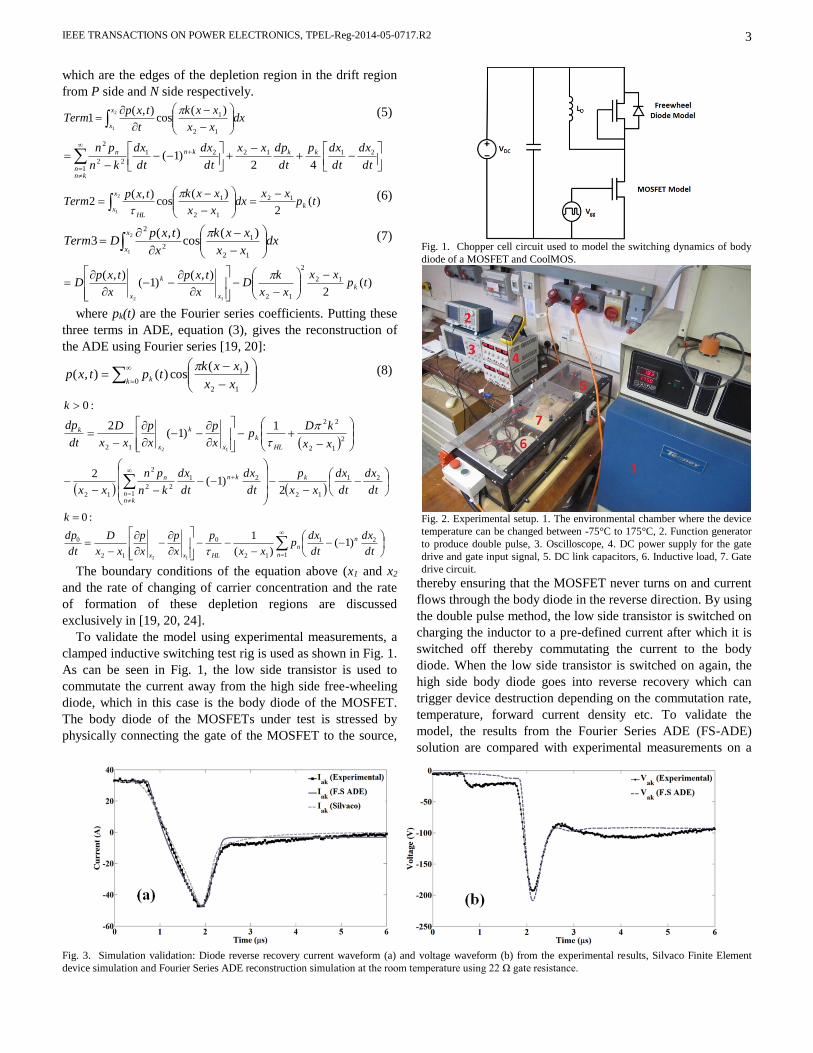
clamped inductive switching test rig is used as shown in Fig. 1.
As can be seen in Fig. 1, the low side transistor is used to
commutate the current away from the high side free-wheeling
diode, which in this case is the body diode of the MOSFET.
The body diode of the MOSFETs under test is stressed by
physically connecting the gate of the MOSFET to the source,
thereby ensuring that the MOSFET never turns on and current
flows through the body diode in the reverse direction. By using
the double pulse method, the low side transistor is switched on
charging the inductor to a pre-defined current after which it is
switched off thereby commutating the current to the body
diode. When the low side transistor is switched on again, the
high side body diode goes into reverse recovery which can
trigger device destruction depending on the commutation rate,
temperature, forward current density etc. To validate the
model, the results from the Fourier Series ADE (FS-ADE)
solution are compared with experimental measurements on a
Fig. 1. Chopper cell circuit used to model the switching dynamics of body
diode of a MOSFET and CoolMOS.
Fig. 2. Experimental setup. 1. The environmental chamber where the device
temperature can be changed between -75°C to 175°C, 2. Function generator
to produce double pulse, 3. Oscilloscope, 4. DC power supply for the gate
drive and gate input signal, 5. DC link capacitors, 6. Inductive load, 7. Gate
drive circuit.
Fig. 3. Simulation validation: Diode reverse recovery current waveform (a) and voltage waveform (b) from the experimental results, Silvaco Finite Element
device simulation and Fourier Series ADE reconstruction simulation at the room temperature using 22 Ω gate resistance.
IEEE TRANSACTIONS ON POWER ELECTRONICS, TPEL-Reg-2014-05-0717.R2
4
discrete PiN diode as well as a finite element device modelled
using a simulator (Silvaco). A 1.2kV/45A IXYS PiN diode
(DSI45-12a) coupled with a low side transistor of suitable
rating was tested. All the terminal voltages and currents were
captured on a Tektronix oscilloscope. The semiconductor
devices were placed in a thermal chamber where the ambient
temperature was varied in order to analyse the temperature
dependencies of the switching transients [22, 23, 25, 26]. Fig.
2 shows the experiment setup including the test rig, chopper
cell, the environmental chamber and the oscilloscope used to
carry out the measurements on the power devices.
Fig. 3(a) shows a comparison of the diode turn-off current
for the experimental measurement, the FS-ADE model and a
finite element simulation from Silvaco while Fig. 3(b) shows a
comparison of the voltage across the device during turn-off.
Datasheet parameters were used together with known physical
constants to obtain matching and the dI/dt of the current was
varied by the gate resistance used to switch the low side
transistor. As can be seen from Fig. 3(a) and Fig. 3(b), the FS-
ADE model is capable of replicating the current and voltage
waveforms of both the experimental measurements as well as
finite element models.
Fig. 4(a) shows the different reverse recovery waveforms of
the discrete silicon PiN diode corresponding to different
commutation rates modulated by the gate resistance of the low
side transistor. The reverse recovery characteristic of the body
diode of a SiC MOSFET from Cree (C2M0160120D) is also
modelled using the FS-ADE solution and validated by
experimental measurements. Fig. 4(b) shows the results of the
FS-ADE model together with the measurements of the reverse
recovery characteristics of the SiC body diode. As can be seen
in Fig. 4(a) and Fig. 4(b), there is good matching between the
FS- ADE model and the experimental measurements. The
material parameters were changed to match with the known
material parameters of SiC and the size of the device was
changed accordingly using the existing data available on the
device datasheet. Fig. 5(a) shows the measured reverse
recovery characteristics of the CoolMOS body diode at
different temperatures whereas Fig. 5(b) shows that of the SiC
MOSFET body diode at different temperatures. As can be seen
from the experimental measurements in Fig. 5(b), there is very
little reverse recovery charge in the SiC body diode compared
with the CoolMOS body-diode shown in Fig. 5(a) and the
reverse characteristics of the SiC MOSFET body diode are
temperature invariant. This is due to the very low minority
carrier lifetime in SiC which means that the stored charge in
the drift region very quickly recombines during the turn-off of
the body diode. Furthermore, the epitaxial voltage blocking
drift layers in SiC are significantly thinner compared to that of
silicon or CoolMOS, hence, there is less charge to be extracted
during turn-off. The model developed for the silicon
CoolMOS body diodes also takes the temperature dependency
of the reverse recovery characteristics into account. As can be
seen in Fig 5(a), the CoolMOS device exhibits significant
reverse recovery charge that increases with temperature due to
increased carrier lifetime. For CoolMOS devices,
modifications have been made to the Fourier solution of the
ADE to account for the fact that it is not the conventional body
diode, but rather alternate PN-N and PP-N diodes due to the
super-junction architecture. Fig. 6(a) shows the structure of the
Fig. 4(a). PiN diode reverse recovery waveform for different IGBT gate resistances (different dI/dt) - Comparison between the experimental results and the
simulation results using the Fourier Series ADE reconstruction. Fig. 4(b). Measured and modeled reverse recovery characteristics of the SiC MOSFET body-
diode.
Fig. 5(a). Measured reverse recovery current as a function of time for the CoolMOS body diode at different temperatures. Fig. 5(b). Measured reverse recovery
current as a function of time for the SiC MOSFET body diode at different temperatures.
IEEE TRANSACTIONS ON POWER ELECTRONICS, TPEL-Reg-2014-05-0717.R2
5
conventional power MOSFET while Fig. 6(b) shows the
structure of a CoolMOS device with the PP-N and PN-N
diodes along with the parasitic BJT, body resistance and
depletion capacitance. According to this structure, the device
consists of a PN-N and PP-N diodes in parallel, due to the
super-junction architecture, i.e. the minority carriers in the PN-
N diodes are holes while the minority carriers in the PP-N
diodes are electrons. Consequently, the minority carrier
lifetime and mobility of these carriers are different in the drift
regions of the two different diodes. The electrons in the PP-N
diodes have a higher lifetime and larger diffusivity in
comparison to holes in the PN-N diodes. The model takes
account of the larger charge stored in the body diode of a
CoolMOS by utilising these two parallel diodes. Basically, in
order to model the PP-N diode structure in the body diode of a
CoolMOS, the N type drift layer of a conventional PiN diode
is replaced with a P-type material with a different background
doping and the minority carriers are changed to electrons. This
means that the diffusion coefficient (related to the mobility of
carriers according to Einstein relationship for diffusion) and
the carrier lifetime are changed (i.e. μn=1330 cm2/Vs and
μp=450 cm2/Vs, τn (P-type)=10μs and τp (N-type)=1μs) [18, 19,
24, 27, 28]. Equation (8) is solved for PN-N and PP-N diodes
keeping in mind that holes are the minority carriers in the
former and electrons are the minority carriers in the latter.
These modifications can account for a significantly higher
reverse recovery charge in CoolMOS which is necessary for
modelling the body diode failure during the reverse recovery.
The model is built in Matlab Simulink and is solved using
variable time steps. At the end of each time step, the carrier
Fig. 8. (a) CoolMOS switching-off current and voltage waveform showing high dI/dt and dV/dt at the same instant of time (b) Instantaneous switching power of
CoolMOS during the switching-off.
Fig. 6. (a) A vertical MOSFET structure, (b) CoolMOS structure including the parasitic BJT and a body diode. (c) Equivalent circuit of a MOSFET with the
parasitic BJT and a body diode.
Fig. 7. Carrier concentration profile in the drift region of a PP-N and PN-N body diodes of a CoolMOS (a) and the carrier concentration profile of a SiC
MOSFET body diode during the high level injection of these devices before switching off.
IEEE TRANSACTIONS ON POWER ELECTRONICS, TPEL-Reg-2014-05-0717.R2
6
concentration in the drift region of the PiN diode, p(x,t), is
calculated using Fourier series reconstruction of the ADE in
(8). Moreover, the boundary conditions of this equation are
calculated at the end of each step and are fed back to the
equation to be used in the next time step. The boundary
conditions are the position of the depletion region at PN- and
NN- junctions (x1 and x2 respectively) and the rate of change of
the depletion width at these junctions (dp1/dt and dp2/dt).
Using the data at each time step, the carrier concentration
profile of the minority carriers in the drift region can be
reconstructed and is shown in Fig. 6.
Fig. 7(a) shows the simulated minority carrier concentration
profiles of the CoolMOS device PP-N and PN-N body diodes
in the drift region whereas Fig. 7(b) shows the minority carrier
concentration profile of the SiC PN-N body diode. The
minority carrier profile in the plasma region of the devices is
extracted right at the point before the devices are switched off
from high level injection mode during body diode conduction.
As can be seen, the carrier concentration profile for PP-N
diode is higher than PN-N diode and hence the reverse
recovery waveform of CoolMOS is higher than a normal
silicon or SiC based PiN diode. This is confirmed by the
experimental measurements on reverse recovery in the body
diodes shown in Fig. 5(a) and Fig. 5(b). The higher minority
carrier concentration in the PP-N relative to the PN-N diode is
due to increased electron lifetime and higher electron
diffusivity. Fig. 7(b) shows that the minority carrier
concentration in the SiC PiN body diode is an order of
magnitude lower than that in the CoolMOS.
III. BJT ELECTRO-THERMAL MODEL
The Fourier series solution to the ADE in PiN body diode
has been used to explore the physics of MOSFET failure
during the reverse recovery of the body diode. Fig. 6(a) shows
a typical vertical MOSFET illustrating the anti-parallel body
diode and body resistance. Referring to Fig. 6(a), the p-well
resistance is shown as Rpb and the drain-base capacitance is
shown as CB. The base current that triggers the BJT can come
from the displacement current of the drain-to-body depletion
capacitance during the body diode turn-off with high dV/dt. It
can also be triggered by high dV/dt across the body diode
during reverse recovery. As the reverse current reaches its
peak, the depletion widths start to form across the junctions of
the PiN diode and the remaining minority carriers in the drift
region have to be recombined since carrier extraction is no
longer possible. If the positive sloping recovery current (the
recombination current between the peak reverse current and
zero) is excessively high in the presence of parasitic
inductance, large voltage overshoots coinciding with high peak
reverse currents can cause very high instantaneous power
dissipation across the device. This high instantaneous power
causes high temperature excursions that can trigger the
parasitic BJT and destroy the device.
Fig. 8(a) shows the measured characteristics of a CoolMOS
body diode in reverse recovery showing high reverse recovery
current and simultaneously high peak voltage overshoot.
Excessively snappy body diodes are known to be a reliability
hazard under hard commutation [29]; hence, soft recovery
diodes have been developed to mitigate this effect. The
electro-thermal modelling of the BJT therefore requires an
accurate physics based modelling of the diode’s reverse
recovery characteristics. To accurately model the electro-
thermal BJT, the displacement current of the drain-to-body
capacitance as a function of dV/dt during turn-off must first be
calculated. Fig. 9(a) to 9(d) shows the results of the FS-ADE
simulations for 2 different switching rates (dI/dt). As the body
diode is switched off, the low carrier lifetime in SiC results in
a rapid extraction of the excess charge. The result of this is a
fast rising voltage with a high dV/dt across the diode that is
proportional to the switching rate. This can be seen in Fig. 9(b)
where the overshoot is due to stray inductance (approximately
between 100-200 nH). The peak overshoot increases with
increasing dI/dt. As the diode begins to block, the electric
fields at the junctions (PN- and N-N+) cause the depletion
width to start extending into the drift region. The result is that
the drain-body capacitance decreases and there is a resulting
displacement current associated with the charging of the
capacitance. Fig. 9(c) shows the simulated drain-base
capacitance whereas Fig. 9(d) shows the calculated
displacement current. The depletion width (Wd1) and the drain-
base capacitance (CB) can be calculated using (9) and (10)
below:
DA
DAd
NN
NN
q
EW 0
1
(9)
1d
iB
WC
(10)
In (9) and (10), NA (SiC: 2×1017 cm-3 and Si: 2×1019 cm-3)
and ND (SiC: 1.5×1015 cm-3 and Si: 1×1013 cm-3) are the donor
and acceptor doping of the P and N- region respectively; q is
unit electron charge; ε is permittivity of SiC/Si (8.5845×10⁻¹³
Fig. 9. Fourier series ADE simulation of the SiC MOSFET body diode
displacement current, parasitic BJT base capacitance and electric field at
P+N- junction during turn-off.
IEEE TRANSACTIONS ON POWER ELECTRONICS, TPEL-Reg-2014-05-0717.R2
7
F/cm and 1.05×10⁻¹² F/cm respectively); and E0 is the electric
field at the metallurgical junction. As the depletion region
widens, the base capacitance of the BJT decreases as shown in
Fig. 9(c). The displacement current at the PN- junction can
cause the parasitic BJT to latch-up if there is sufficient body
resistance to forward bias the parasitic BJT. This causes BJT
latch-up of the device by causing a voltage drop across the
emitter-base junction of the BJT greater than the in-built
voltage (φBE). The displacement current shown in Fig. 9(d) is
calculated using (11) below. In this equation, A represents die
area and a ratio between the cell size and the P-emitter of the
body diode is considered as the die area of the body diode
(SiC MOSFET die area is approximately 10.24 mm2 and
CoolMOS is approximately 20 mm2 and the body diode ratio is
assumed to be in the range of 10-20%). Neff is the effective
doping of the depletion region, VCE and VDS are BJT’s
collector-emitter and MOSFET’s drain-source voltages
respectively.
dt
dV
V
qNA
dt
dV
W
AI DS
CE
effDSdisp
2
(11)
It can be seen from Fig. 9(d) that the peak displacement
current increases with the switching rate. This means that
faster switching devices are more likely to undergo parasitic
BJT latch-up. That displacement current flows through the
body resistance (Rpb) of the MOSFET which is the resistance
between the p-body and the n-source. This p-body resistance
(Rpb) can be calculated using (12) where L is the length of the
base (0.9×10⁻⁴ cm), NB is the base doping (2×1017 cm-3) and AB
is the area of the base:
BBp
pbANq
LR
(12)
The mobility of holes (µp) in the base of the BJT is
temperature dependent. Consequently, increasing the
temperature reduces the hole mobility, hence increasing the
base resistance. This increases the base-emitter voltage of the
BJT. The temperature dependence of μp [30] is shown in (13).
The critical MOSFET parameter that contributes to avalanche
breakdown is the body resistance, which must be minimized
for a rugged MOSFET. In the equation below, index of i,
indicates holes or electrons. T is temperature of the device,
Npg, γp, αp, and βp depends on type of the material and N is the
dopant concentration.
)(
)(
)(
max,
3001
300iiT
B
TB
Ni
iNi
ii
(13)
KT
pg
pg
pp
p
Nip
p
N
N
N
N
B
300
min,max,
max,
)( 1
1
5.0)4( SiCHp
6.2)4( SiCHp
5.0)4( SiCHp
112
max, 117)4( sVcmSiCHp
112
min, 30)4( sVcmSiCHp
31910)4( cmSiCHN pg
317102 cmNN B
By multiplying the body-resistance in the displacement
current induced by the P+N¬- junction of the PiN body diode,
the base-emitter voltage (VBE) of the BJT is calculated.
pbdispBE RIV (14)
The built-in voltage φbi of the parasitic BJT can be
calculated using (15) below:
2ln
i
EBbi
n
NN
q
KT (15)
where K is Boltzmann constant, NB and NE (1.2×1019 cm-3)
are the base and emitter doping respectively and ni is the
intrinsic carrier concentration which is also temperature
dependent and increases with temperature (T). Equation (16)
shows this temperature dependency [17]. T
i eTSiCHn /)1008.2(2/316 4
107.1)4( (16)
If the voltage drop across the base-emitter of the BJT
becomes greater than the built-in voltage of the parasitic BJT,
then the BJT switches on and a current starts flowing from the
collector to the emitter of the BJT. In the proposed electro-
thermal model, the Ebers-Moll model is used to calculate the
collector current. In the equation below VT is thermal voltage.
The applicability of Ebers-Moll model for large signal
modelling is shown in [31-34].
1T
biBE
V
V
ESFC eII
(17)
BB
ib
EE
ieES
NW
nD
NL
nDqAI
22 (18)
De and Db are diffusion coefficients which are related to the
electron mobility in the emitter and base of the parasitic BJT
using Einstein relation (kinetic theory). LE is emitter length, NE
is emitter doping and WB is the base width of the BJT. The
electron mobility can be calculated using (19) in which ND is
donor doping.
Eneq
KTD ,
(19)
Bnbq
KTD ,
61.010
61.013
,1055.3
201005.4)4(
D
DEn
N
NSiCH
317
, 102: cmNDBn
319
, 102: cmNDEn
As the BJT turns on, the current passing through the device
generates heat and the device temperature starts rising which
increases the base resistance and the body voltage.
Consequently, the positive feedback loop increases the
parasitic BJT forward current. This continues to generate more
power until the temperature excursion due to the instantaneous
power causes the device to break down. The calculated power
is inserted into Cauer-network to model the junction
IEEE TRANSACTIONS ON POWER ELECTRONICS, TPEL-Reg-2014-05-0717.R2
8
temperature of the chip. Fig. 10 illustrates the cross section
view of a basic hypothetical power device mounted on top of a
DBC and the equivalent Cauer-network of this power module.
The flow chart of the model developed in Simulink is shown in
Fig. 11. As can be seen in this figure, the temperature
calculated from the thermal network [35] is fed back in a
closed loop to recalculate the temperature dependent
parameters in the clamped inductive circuit, base resistance,
intrinsic carrier concentration and the BJT base and collector
currents. As can be seen in Fig. 11, if the BJT does not latch-
up, then the current continues to flow in the body diode until it
reaches zero and the simulation model works in Loop1 showed
in the figure. The values of thermal resistors and capacitors
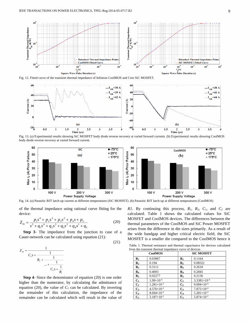
for the Cauer-network are calculated by taking these steps:
Step 1- finite sample points from the transient thermal
impedance curve (junction to case) obtained from a single
pulse power input of the power device was captured from the
device datasheet (Cree SiC MOSFET and Infineon CoolMOS
CE technology).
Step 2- Using curve fitting tool in MATLAB, a rational
fitting method is used to reconstruct the curve (Fig. 12). Here
Cauer-network impedance equation is considered to be the
base of curve fitting as it can give physical meaning to each
layer; however, Foster network may be used as well. Each
parameter in the curve fitting tool is set to have an upper and
lower limits based on the geometry, specific heat capacity,
density and thermal conductance of the material to achieve
reasonable values for thermal resistance and thermal
capacitance of the Cauer-network thermal chain. Note that
based on the Cauer-network impedance equation, the
numerator degree is one order smaller than the denominator
degree. It is critical for this study to have an accurate curve
fitting within the µs level as the transient occurs in µs.
Consequently, 5th order Cauer network is considered for both
SiC MOSFET and CoolMOS which in case of TO-247 may be
interpreted as the die, solder layer, adhesive layer, the copper
base plate, CTE-matched high flow EMC (epoxy moulding
compound) packaging. Equation (20) shows the reconstruction
Fig. 10. Cross section view of a basic hypothetical die mounted on top of a DBC and soldered to a base plate and the corresponding Cauer-network of this power
module.
Fig. 11. Block diagram of the electro-thermal parasitic BJT latch-up coupled with the clamped inductive switching circuit model for a MOSFET body diode.
IEEE TRANSACTIONS ON POWER ELECTRONICS, TPEL-Reg-2014-05-0717.R2
9
of the thermal impedance using rational curve fitting for the
device:
5
1
4
2
3
3
2
4
1
5
54
2
3
3
2
4
1
qsqsqsqsqs
pspspspspZ th
(20)
Step 3- The impedance from the junction to case of a
Cauer-network can be calculated using equation (21):
i
i
th
RsC
R
sC
Z
1
1...
1
1
1
1
1
'
(21)
Step 4- Since the denominator of equation (20) is one order
higher than the numerator, by calculating the admittance of
equation (20), the value of C1 can be calculated. By inverting
the remainder of this calculation, the impedance of the
remainder can be calculated which will result in the value of
R1. By continuing this process, R1, R2, C1, and C2 are
calculated. Table 1 shows the calculated values for SiC
MOSFET and CoolMOS devices. The differences between the
thermal parameters of the CoolMOS and SiC Power MOSFET
arises from the difference in die sizes primarily. As a result of
the wide bandgap and higher critical electric field, the SiC
MOSFET is a smaller die compared to the CoolMOS hence it
Table. 1. Thermal resistance and thermal capacitance for devices calculated
from the transient thermal impedance curve of devices
CoolMOS SiC MOSFET
R1 0.03867 R1 0.1164
R2 0.194 R2 0.08321
R3 0.3111 R3 0.2618
R4 0.4003 R4 0.2845
R5 0.02277 R5 0.2136
C1 1.99×10⁻⁴ C1 3.3381×10⁻⁴
C2 1.281×10⁻³ C2 9.084×10⁻⁴
C3 4.576×10⁻³ C3 7.875×10⁻⁴
C4 8.694×10⁻³ C4 5.281×10⁻³
C5 3.187×10⁻¹ C5 5.874×10⁻²
Fig. 12. Fitted curve of the transient thermal impedance of Infineon CoolMOS and Cree SiC MOSFET.
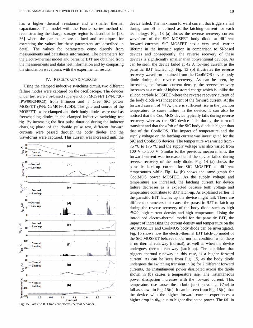
Fig. 13. (a) Experimental results showing SiC MOSFET body diode reverse recovery at varied forward currents. (b) Experimental results showing CoolMOS
body diode reverse recovery at varied forward current.
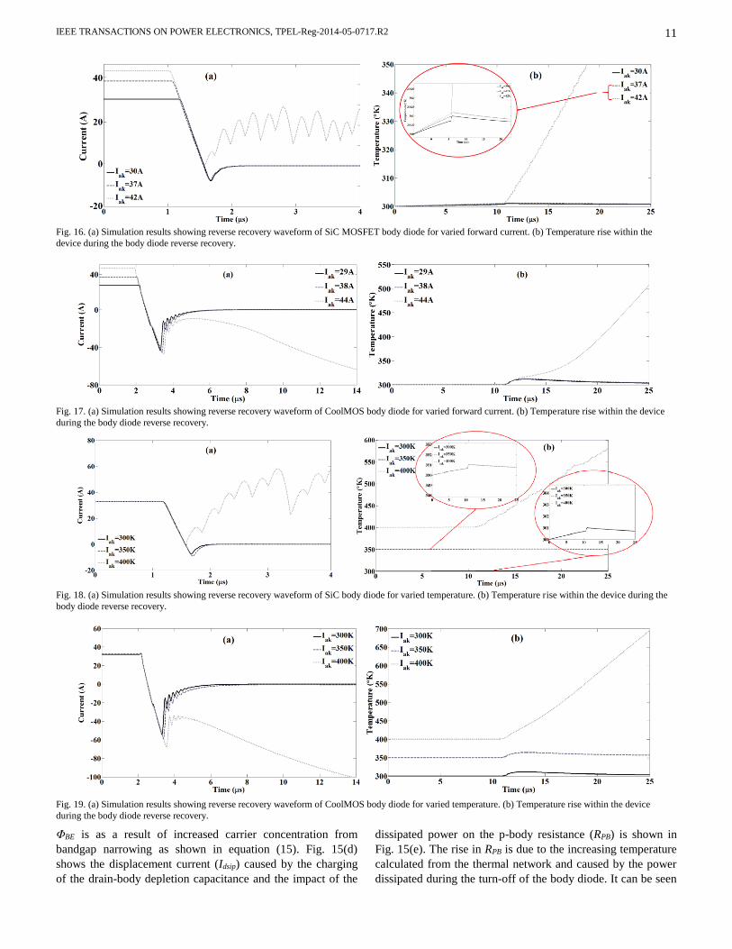
Fig. 14. (a) Parasitic BJT latch-up current at different temperatures (SiC MOSFET). (b) Parasitic BJT latch-up at different temperatures (CoolMOS)
IEEE TRANSACTIONS ON POWER ELECTRONICS, TPEL-Reg-2014-05-0717.R2
10
has a higher thermal resistance and a smaller thermal
capacitance. The model with the Fourier series method of
reconstructing the charge storage region is described in [28,
36] where the parameters are defined and techniques for
extracting the values for these parameters are described in
detail. The values for parameters come directly from
measurements and datasheets information. The parameters for
the electro-thermal model and parasitic BJT are obtained from
the measurements and datasheet information and by comparing
the simulation waveforms with the experimental results.
IV. RESULTS AND DISCUSSION
Using the clamped inductive switching circuit, two different
failure modes were captured on the oscilloscope. The devices
under test were a Si-based super-junction MOSFET (P/N: 726-
IPW90R340C3) from Infineon and a Cree SiC power
MOSFET (P/N: C2M0160120D). The gate and source of the
MOSFETs were clamped and their body diodes were used as
freewheeling diodes in the clamped inductive switching test
rig. By increasing the first pulse duration during the inductor
charging phase of the double pulse test, different forward
currents were passed through the body diodes and the
waveforms were captured. This current was increased until the
device failed. The maximum forward current that triggers a fail
during turn-off is defined as the latching current for each
technology. Fig. 13 (a) shows the reverse recovery current
waveform of the SiC MOSFET body diode at different
forward currents. SiC MOSFET has a very small carrier
lifetime in the intrinsic region in comparison to Si-based
devices and consequently, the reverse recovery of these
devices is significantly smaller than conventional devices. As
can be seen, the device failed at 42 A forward current as the
parasitic BJT latched up. Fig. 13 (b) illustrates the reverse
recovery waveform obtained from the CoolMOS device body
diode during the reverse recovery. As can be seen, by
increasing the forward current density, the reverse recovery
increases as a result of higher stored charge which is unlike the
silicon carbide MOSFET where the reverse recovery current of
the body diode was independent of the forward current. At the
forward current of 44 A, there is sufficient rise in the junction
temperature to cause failure in the device. It can also be
noticed that the CoolMOS device typically fails during reverse
recovery whereas the SiC device fails during the turn-off
transient and that the dI/dt of the SiC body diode is higher than
that of the CoolMOS. The impact of temperature and the
supply voltage on the latching current was investigated for the
SiC and CoolMOS devices. The temperature was varied from -
75 °C to 175 °C and the supply voltage was also varied from
100 V to 300 V. Similar to the previous measurements, the
forward current was increased until the device failed during
reverse recovery of the body diode. Fig. 14 (a) shows the
parasitic latch-up current for SiC MOSFET at different
temperatures while Fig. 14 (b) shows the same graph for
CoolMOS power MOSFET. As the supply voltage and
temperature are increased, the latching current for device
failure decreases as is expected because both voltage and
temperature contribute to BJT latch-up. As explained earlier, if
the parasitic BJT latches up the device might fail. There are
different parameters that cause the parasitic BJT to latch up
during the reverse recovery of the body diode such as high
dV/dt, high current density and high temperature. Using the
introduced electro-thermal model for the parasitic BJT, the
impact of increasing the current density and temperature on the
SiC MOSFET and CoolMOS body diode can be investigated.
Fig. 15 shows how the electro-thermal BJT latch-up model of
the SiC MOSFET behaves under normal condition when there
is no thermal runaway (normal), as well as when the device
undergoes thermal runaway (latch-up). The condition that
triggers thermal runaway in this case, is a higher forward
current. As can be seen from Fig. 15, as the body diode
undergoes the switching transient in (a) for 2 different forward
currents, the instantaneous power dissipated across the diode
shown in (b) causes a temperature rise. The instantaneous
power dissipation increases with the forward current. This
temperature rise causes the in-built junction voltage (ΦBE) to
fall as shown in Fig. 15(c). It can be seen from Fig. 15(c), that
the device with the higher forward current experiences a
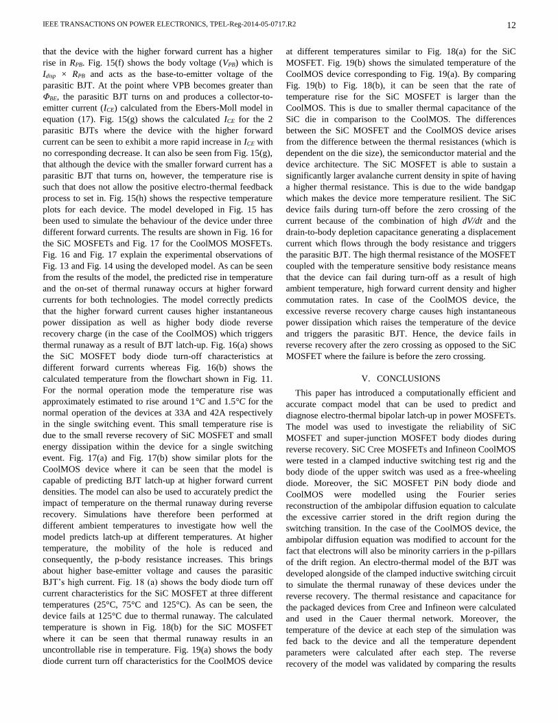
higher drop in ΦBE due to higher dissipated power. The fall in Fig. 15. Parasitic BJT transient electro-thermal behavior.
IEEE TRANSACTIONS ON POWER ELECTRONICS, TPEL-Reg-2014-05-0717.R2
11
ΦBE is as a result of increased carrier concentration from
bandgap narrowing as shown in equation (15). Fig. 15(d)
shows the displacement current (Idsip) caused by the charging
of the drain-body depletion capacitance and the impact of the
dissipated power on the p-body resistance (RPB) is shown in
Fig. 15(e). The rise in RPB is due to the increasing temperature
calculated from the thermal network and caused by the power
dissipated during the turn-off of the body diode. It can be seen
Fig. 16. (a) Simulation results showing reverse recovery waveform of SiC MOSFET body diode for varied forward current. (b) Temperature rise within the
device during the body diode reverse recovery.
Fig. 17. (a) Simulation results showing reverse recovery waveform of CoolMOS body diode for varied forward current. (b) Temperature rise within the device
during the body diode reverse recovery.
Fig. 18. (a) Simulation results showing reverse recovery waveform of SiC body diode for varied temperature. (b) Temperature rise within the device during the
body diode reverse recovery.
Fig. 19. (a) Simulation results showing reverse recovery waveform of CoolMOS body diode for varied temperature. (b) Temperature rise within the device
during the body diode reverse recovery.
IEEE TRANSACTIONS ON POWER ELECTRONICS, TPEL-Reg-2014-05-0717.R2
12
that the device with the higher forward current has a higher
rise in RPB. Fig. 15(f) shows the body voltage (VPB) which is
Idisp × RPB and acts as the base-to-emitter voltage of the
parasitic BJT. At the point where VPB becomes greater than
ΦBE, the parasitic BJT turns on and produces a collector-to-
emitter current (ICE) calculated from the Ebers-Moll model in
equation (17). Fig. 15(g) shows the calculated ICE for the 2
parasitic BJTs where the device with the higher forward
current can be seen to exhibit a more rapid increase in ICE with
no corresponding decrease. It can also be seen from Fig. 15(g),
that although the device with the smaller forward current has a
parasitic BJT that turns on, however, the temperature rise is
such that does not allow the positive electro-thermal feedback
process to set in. Fig. 15(h) shows the respective temperature
plots for each device. The model developed in Fig. 15 has
been used to simulate the behaviour of the device under three
different forward currents. The results are shown in Fig. 16 for
the SiC MOSFETs and Fig. 17 for the CoolMOS MOSFETs.
Fig. 16 and Fig. 17 explain the experimental observations of
Fig. 13 and Fig. 14 using the developed model. As can be seen
from the results of the model, the predicted rise in temperature
and the on-set of thermal runaway occurs at higher forward
currents for both technologies. The model correctly predicts
that the higher forward current causes higher instantaneous
power dissipation as well as higher body diode reverse
recovery charge (in the case of the CoolMOS) which triggers
thermal runaway as a result of BJT latch-up. Fig. 16(a) shows
the SiC MOSFET body diode turn-off characteristics at
different forward currents whereas Fig. 16(b) shows the
calculated temperature from the flowchart shown in Fig. 11.
For the normal operation mode the temperature rise was
approximately estimated to rise around 1°C and 1.5°C for the
normal operation of the devices at 33A and 42A respectively
in the single switching event. This small temperature rise is
due to the small reverse recovery of SiC MOSFET and small
energy dissipation within the device for a single switching
event. Fig. 17(a) and Fig. 17(b) show similar plots for the
CoolMOS device where it can be seen that the model is
capable of predicting BJT latch-up at higher forward current
densities. The model can also be used to accurately predict the
impact of temperature on the thermal runaway during reverse
recovery. Simulations have therefore been performed at
different ambient temperatures to investigate how well the
model predicts latch-up at different temperatures. At higher
temperature, the mobility of the hole is reduced and
consequently, the p-body resistance increases. This brings
about higher base-emitter voltage and causes the parasitic
BJT’s high current. Fig. 18 (a) shows the body diode turn off
current characteristics for the SiC MOSFET at three different
temperatures (25°C, 75°C and 125°C). As can be seen, the
device fails at 125°C due to thermal runaway. The calculated
temperature is shown in Fig. 18(b) for the SiC MOSFET
where it can be seen that thermal runaway results in an
uncontrollable rise in temperature. Fig. 19(a) shows the body
diode current turn off characteristics for the CoolMOS device
at different temperatures similar to Fig. 18(a) for the SiC
MOSFET. Fig. 19(b) shows the simulated temperature of the
CoolMOS device corresponding to Fig. 19(a). By comparing
Fig. 19(b) to Fig. 18(b), it can be seen that the rate of
temperature rise for the SiC MOSFET is larger than the
CoolMOS. This is due to smaller thermal capacitance of the
SiC die in comparison to the CoolMOS. The differences
between the SiC MOSFET and the CoolMOS device arises
from the difference between the thermal resistances (which is
dependent on the die size), the semiconductor material and the
device architecture. The SiC MOSFET is able to sustain a
significantly larger avalanche current density in spite of having
a higher thermal resistance. This is due to the wide bandgap
which makes the device more temperature resilient. The SiC
device fails during turn-off before the zero crossing of the
current because of the combination of high dV/dt and the
drain-to-body depletion capacitance generating a displacement
current which flows through the body resistance and triggers
the parasitic BJT. The high thermal resistance of the MOSFET
coupled with the temperature sensitive body resistance means
that the device can fail during turn-off as a result of high
ambient temperature, high forward current density and higher
commutation rates. In case of the CoolMOS device, the
excessive reverse recovery charge causes high instantaneous
power dissipation which raises the temperature of the device
and triggers the parasitic BJT. Hence, the device fails in
reverse recovery after the zero crossing as opposed to the SiC
MOSFET where the failure is before the zero crossing.
V. CONCLUSIONS
This paper has introduced a computationally efficient and
accurate compact model that can be used to predict and
diagnose electro-thermal bipolar latch-up in power MOSFETs.
The model was used to investigate the reliability of SiC
MOSFET and super-junction MOSFET body diodes during
reverse recovery. SiC Cree MOSFETs and Infineon CoolMOS
were tested in a clamped inductive switching test rig and the
body diode of the upper switch was used as a free-wheeling
diode. Moreover, the SiC MOSFET PiN body diode and
CoolMOS were modelled using the Fourier series
reconstruction of the ambipolar diffusion equation to calculate
the excessive carrier stored in the drift region during the
switching transition. In the case of the CoolMOS device, the
ambipolar diffusion equation was modified to account for the
fact that electrons will also be minority carriers in the p-pillars
of the drift region. An electro-thermal model of the BJT was
developed alongside of the clamped inductive switching circuit
to simulate the thermal runaway of these devices under the
reverse recovery. The thermal resistance and capacitance for
the packaged devices from Cree and Infineon were calculated
and used in the Cauer thermal network. Moreover, the
temperature of the device at each step of the simulation was
fed back to the device and all the temperature dependent
parameters were calculated after each step. The reverse
recovery of the model was validated by comparing the results
IEEE TRANSACTIONS ON POWER ELECTRONICS, TPEL-Reg-2014-05-0717.R2
13
with the experiments. Experiments show that thermal runaway
is exacerbated by high current densities and temperatures
which is well predicted and replicated by the model.
REFERENCES
[1] C. Xu, L. Xing-Ming, J. K. O. Sin, and K. Bao-wei, "Improving
the CoolMS™ body-diode switching performance with
integrated Schottky contacts," in Power Semiconductor Devices
and ICs, 2003. Proceedings. ISPSD '03. 2003 IEEE 15th
International Symposium on, 2003, pp. 304-307.
[2] T. Funaki, M. Matsushita, M. Sasagawa, T. Kimoto, and T.
Hikihara, "A Study on SiC Devices in Synchronous Rectification
of DC-DC Converter," in Applied Power Electronics Conference,
APEC 2007 - Twenty Second Annual IEEE, 2007, pp. 339-344.
[3] D. De, A. Castellazzi, A. Solomon, A. Trentin, M. Minami, and T.
Hikihara, "An all SiC MOSFET high performance PV converter
cell," in Power Electronics and Applications (EPE), 2013 15th
European Conference on, 2013, pp. 1-10.
[4] C. D. Brown and B. Sarlioglu, "Reducing switching losses in
BLDC motor drives by reducing body diode conduction of
MOSFETs," in Energy Conversion Congress and Exposition
(ECCE), 2013 IEEE, 2013, pp. 4286-4293.
[5] S. Buonomo, S. Musumeci, R. Pagano, C. Porto, A. Raciti, and R.
Scollo, "Driving a New Monolithic Cascode Device in a DC–DC
Converter Application," Industrial Electronics, IEEE
Transactions on, vol. 55, pp. 2439-2449, 2008.
[6] J. Jordan, V. Esteve, E. Sanchis-Kilders, E. J. Dede, E. Maset, J.
B. Ejea, et al., "A Comparative Performance Study of a 1200 V Si
and SiC MOSFET Intrinsic Diode on an Induction Heating
Inverter," Power Electronics, IEEE Transactions on, vol. 29, pp.
2550-2562, 2014.
[7] Z. Jun, C. F. Wheatley, R. Stokes, C. Kocon, and S. Benczkowski,
"Optimization of the body-diode of power MOSFETs for high
efficiency synchronous rectification," in Power Semiconductor
Devices and ICs, 2000. Proceedings. The 12th International
Symposium on, 2000, pp. 145-148.
[8] R. Siemieniec, O. Blank, M. Hutzler, L. J. Yip, and J. Sanchez,
"Robustness of MOSFET devices under hard commutation ofthe
body diode," in Power Electronics and Applications (EPE), 2013
15th European Conference on, 2013, pp. 1-10.
[9] Y. Shaoyong, A. Bryant, P. Mawby, X. Dawei, L. Ran, and P.
Tavner, "An Industry-Based Survey of Reliability in Power
Electronic Converters," Industry Applications, IEEE Transactions
on, vol. 47, pp. 1441-1451, 2011.
[10] Z. Hui and L. M. Tolbert, "Efficiency Impact of Silicon Carbide
Power Electronics for Modern Wind Turbine Full Scale Frequency
Converter," Industrial Electronics, IEEE Transactions on, vol. 58,
pp. 21-28, 2011.
[11] G. Busatto, G. V. Persiano, and F. Iannuzzo, "Experimental and
numerical investigation on MOSFET's failure during reverse
recovery of its internal diode," Electron Devices, IEEE
Transactions on, vol. 46, pp. 1268-1273, 1999.
[12] F. Iannuzzo, G. V. Persiano, and G. Busatto, "Measurement of the
BJT activation current during the reverse recovery of power
MOSFET's drain-source diode," Electron Devices, IEEE
Transactions on, vol. 48, pp. 391-393, 2001.
[13] A. Bryant, "Simulation and Optimisation of Diode and IGBT
Interaction in a Chopper Cell," Doctor of Philosophy, Queens'
College, University of Cambridge, Cambridge, 2005.
[14] G. M. Buiatti, F. Cappelluti, and G. Ghione, "Power PiN diode
model for PSPICE simulations," in Applied Power Electronics
Conference and Exposition, 2005. APEC 2005. Twentieth Annual
IEEE, 2005, pp. 1911-1916 Vol. 3.
[15] A. T. Bryant, G. J. Roberts, A. Walker, and P. A. Mawby, "Fast
Inverter Loss Simulation and Silicon Carbide Device Evaluation
for Hybrid Electric Vehicle Drives," in Power Conversion
Conference - Nagoya, 2007. PCC '07, 2007, pp. 1017-1024.
[16] P. A. Mawby, P. M. Igic, and M. S. Towers, "Physically based
compact device models for circuit modelling applications,"
Microelectronics Journal, vol. 32, pp. 433-447, 5// 2001.
[17] B. J. Baliga, Fundamentals of Power Semiconductor Devices:
Springer Publishing Company, Incorporated, 2008.
[18] L. Lu, A. Bryant, E. Santi, J. L. Hudgins, and P. R. Palmer,
"Physical Modeling and Parameter Extraction Procedure for p-i-n
Diodes with Lifetime Control," in Industry Applications
Conference, 2006. 41st IAS Annual Meeting. Conference Record
of the 2006 IEEE, 2006, pp. 1450-1456.
[19] A. T. Bryant, P. R. Palmer, E. Santi, and J. L. Hudgins, "A
Compact Diode Model for the Simulation of Fast Power Diodes
including the Effects of Avalanche and Carrier Lifetime Zoning,"
in Power Electronics Specialists Conference, 2005. PESC '05.
IEEE 36th, 2005, pp. 2042-2048.
[20] A. T. Bryant, L. Liqing, E. Santi, P. R. Palmer, and J. L. Hudgins,
"Physical Modeling of Fast p-i-n Diodes With Carrier Lifetime
Zoning, Part I: Device Model," Power Electronics, IEEE
Transactions on, vol. 23, pp. 189-197, 2008.
[21] P. A. Mawby, A. T. Bryant, P. R. Palmer, E. Santi, and J. L.
Hudgins, "High Speed Electro-Thermal Models for Inverter
Simulations," in Microelectronics, 2006 25th International
Conference on, 2006, pp. 166-173.
[22] P. M. Igic, P. A. Mawby, M. S. Towers, and S. Batcup, "Dynamic
electro-thermal physically based compact models of the power
devices for device and circuit simulations," in Semiconductor
Thermal Measurement and Management, 2001. Seventeenth
Annual IEEE Symposium, 2001, pp. 35-42.
[23] A. Bryant, N. A. Parker-Allotey, D. Hamilton, I. Swan, P. A.
Mawby, T. Ueta, et al., "A Fast Loss and Temperature Simulation
Method for Power Converters, Part I: Electrothermal Modeling and
Validation," Power Electronics, IEEE Transactions on, vol. 27,
pp. 248-257, 2012.
[24] A. T. Bryant, P. R. Palmer, E. Santi, and J. L. Hudgins,
"Simulation and Optimization of Diode and Insulated Gate Bipolar
Transistor Interaction in a Chopper Cell Using MATLAB and
Simulink," Industry Applications, IEEE Transactions on, vol. 43,
pp. 874-883, 2007.
[25] Z. Zhou, M. S. Khanniche, P. Igic, S. T. Kong, M. Towers, and P.
A. Mawby, "A fast power loss calculation method for long real
time thermal simulation of IGBT modules for a three-phase
inverter system," in Power Electronics and Applications, 2005
European Conference on, 2005, pp. 9 pp.-P.10.
[26] A. N. Githiari, B. M. Gordon, R. A. McMahon, L. Zhong-Min,
and P. A. Mawby, "A comparison of IGBT models for use in
circuit design," Power Electronics, IEEE Transactions on, vol. 14,
pp. 607-614, 1999.
[27] T. Gachovska, J. L. Hudgins, A. Bryant, E. Santi, H. A. Mantooth,
and A. K. Agarwal, "Modeling, Simulation, and Validation of a
Power SiC BJT," Power Electronics, IEEE Transactions on, vol.
27, pp. 4338-4346, 2012.
[28] A. T. Bryant, K. Xiaosong, E. Santi, P. R. Palmer, and J. L.
Hudgins, "Two-step parameter extraction procedure with formal
optimization for physics-based circuit simulator IGBT and p-i-n
diode models," Power Electronics, IEEE Transactions on, vol. 21,
pp. 295-309, 2006.
[29] Z. Xi, J. Lei, D. Junjun, L. Siqi, and C. Zheng, "Analysis and
Design of a New Soft-Switching Boost Converter With a Coupled
Inductor," Power Electronics, IEEE Transactions on, vol. 29, pp.
4270-4277, 2014.
[30] T. T. Mnatsakanov, L. I. Pomortseva, and S. N. Yurkov,
"Semiempirical model of carrier mobility in silicon carbide for
analyzing its dependence on temperature and doping level,"
Semiconductors, vol. 35, pp. 394-397, 2001/04/01 2001.
[31] I. E. Getreu, Modeling the bipolar transistor: Elsevier Scientific
Pub. Co., 1978.
[32] R. L. Bailey, "Large-signal nonlinear analysis of a high-power
high-frequency junction transistor," Electron Devices, IEEE
Transactions on, vol. 17, pp. 108-119, 1970.
[33] C. D. Root, J. Melillo, and S. Sammon, "Computer modeling of
diode forward recovery characteristics," Electron Devices, IEEE
Transactions on, vol. 29, pp. 461-463, 1982.
[34] T. Shih-Wei, C. Hon-Rung, C. Wei-Tien, H. Meng-Kai, L. An-
Hung, W. Lour, et al., "Characterization and modeling of three-
terminal heterojunction phototransistors using an InGaP layer for
IEEE TRANSACTIONS ON POWER ELECTRONICS, TPEL-Reg-2014-05-0717.R2
14
passivation," Electron Devices, IEEE Transactions on, vol. 52, pp.
204-210, 2005.
[35] A. Merkert, T. Krone, and A. Mertens, "Characterization and
Scalable Modeling of Power Semiconductors for Optimized
Design of Traction Inverters with Si- and SiC-Devices," Power
Electronics, IEEE Transactions on, vol. 29, pp. 2238-2245, 2014.
[36] A. T. Bryant, P. R. Palmer, J. L. Hudgins, E. Santi, and X. Kang,
"The use of a formal optimisation procedure in automatic
parameter extraction of power semiconductor devices," in Power
Electronics Specialist Conference, 2003. PESC '03. 2003 IEEE
34th Annual, 2003, pp. 822-827 vol.2.
Roozbeh Bonyadi (S'14) graduated his 1st class
BSc honours degree in Electrical-Electronics
Engineering from Shahed University of Tehran.
Following this, he came to England to undertake
his MSc degree, graduating with a Merit in
Electronic Systems at the University of Warwick,
UK. His MSc project was intelligent fault
diagnosis in automotive electronic systems of
systems of premium vehicles in collaboration with
Jaguar Land Rover PLC. After his graduation he
started working as a KTP associate at the
University of Wolverhampton in collaboration with Phoenix Calibration \&
Services Ltd. His interest in hybrid/electric vehicles and semiconductor
devices and power module packaging led him to undertake a PhD in Power
Electronics at the University of Warwick. His PhD project is sponsored by
EPSRC in collaboration with Jaguar Land Rover and involves design,
simulation, implementation and packaging of automotive power inverters. He
is a member of the IEEE, IAS, and PELS.
Olayiwola Alatise (M'05) received the B.Eng.
degree (with first-class honors) in electronic
engineering and the Ph.D. degree in
microelectronics and semiconductors from
Newcastle University, U.K., in 2008. His research
focused on mixed-signal performance
enhancements in strained Si/SiGe metal–oxide–
semiconductor field-effect transistors (MOSFETs).
In June 2008, he joined the Innovation R\&D
Department, NXP Semiconductors, as a
Development Engineer, where he designed, processed, and qualified discrete
power trench MOSFETs for automotive applications and switched-mode
power supplies. In November 2010, he became a Science City Research
Fellow with the University of Warwick and since August 2012, he is serving
as assistant professor of Electrical Engineering in University of Warwick,
Coventry, U.K. His research interest include investigating advanced power
semiconductor materials and devices for improved energy conversion
efficiency.
Saeed Jahdi (S'10) received the BSc degree in
Electrical Power Engineering from University of
Science and Technology, Tehran, Iran, in 2005 and
the degree of MSc with distinction in Power
Systems and Energy Management from City
University London, U.K., in 2012. Since then, he is
pursuing the Ph.D. degree in electrical engineering
as a candidate in Power Electronics laboratory of
School of Engineering of University of Warwick,
U.K. while he has been awarded an energy theme
scholarship for the duration of his research. His current research interests
include wide band-gap semiconductor devices in high voltage power
converters, circuits and applications. He is currently working on Silicon
Carbide based Solid State Fault Current Limiters, with collaboration with
Western Power Distribution (WPD), UK. Mr. Jahdi is a member of IEEE
Power Electronics and IEEE Industrial Electronics societies.
Ji Hu was born in 1989 in Lianyungang, China.
He received the bachelor degree in Electronic and
Electrical Engineering from the Northumbria
University in 2011, and received master degree in
Energy and Power Electronics from University of
Warwick in 2013. He is currently working as PhD
researcher on power electronics in University of
Warwick.
Jose Angel Ortiz Gonzalez received a degree in
Electrical Engineering in 2009 from the University
of Vigo, Vigo, Spain. From 2010 to 2012 he
worked as a Support Technician at the Department
of Electronics Technology, University of Vigo,
Spain. Since 2013 he has been working at the
School of Engineering, University of Warwick,
Coventry, United Kingdom as a Senior Power
Electronics Research Technician currently focusing
on high voltage silicon carbide based DC-DC and
DC-AC power converters. His current research
interests include power converters, circuit testing
and device evaluation.
Li Ran (M'98-SM'07) received a PhD degree in
Power Systems Engineering from Chongqing
University, Chongqing, China, in 1989. He was a
Research Associate with the Universities of
Aberdeen, Nottingham and Heriot-Watt, at
Aberdeen, Nottingham and Edinburgh in the UK
respectively. He became a Lecturer in Power
Electronics with Northumbria University,
Newcastle upon Tyne, the UK in 1999 and was
seconded to Alstom Power Conversion, Kidsgrove,
UK in 2001. Between 2003 and 2012, he was with
Durham University, UK. He joined the University
of Warwick, Coventry, UK as a Professor in Power Electronics - Systems in
2012. His research interests include the application of Power Electronics for
electric power generation, delivery and utilisation.
Philip Mawby (S'85-M'86-SM'01) received the
B.Sc. and Ph.D. degrees in electronic and electrical
engineering from the University of Leeds, U.K., in
1983 and 1987, respectively. His Ph.D. was
focused on GaAs/AlGaAs heterojunction bipolar
transistors for high-power radio frequency
applications at the GEC Hirst Research Centre,
Wembley, U.K.
In 2005, he joined the University of Warwick,
Coventry, U.K., as the Chair of power electronics.
He was also with the University of Wales,
Swansea, U.K. for 19 years and held the Royal Academy of Engineering
Chair for power electronics, where he established the Power Electronics
Design Center. He has been internationally recognized in the area of power
electronics and power device research. He was also involved in the
development of device simulation algorithms, as well as optoelectronic and
quantum-based device structures. He has authored or coauthored more than
100 journal and conference papers. His current research interests include
materials for new power devices, modeling of power devices and circuits.
Prof. Mawby has been involved in many international conference committees,
including the ISPSD, EPE, and the ESSDERC. He is a Chartered Engineer, a
Fellow of the IET, and a Fellow of the Institute Physics. He is a Distinguished
Lecturer for the IEEE Electron Devices Society.