lab 6 prototyping - twins.ee.nctu.edu.twtwins.ee.nctu.edu.tw/.../lab_6_rapid_prototyping.pdf ·...
TRANSCRIPT
Lab 6 Prototyping
Table of Contents
1. INTRODUCTION...............................................................................................................................1
2. ARM SYSTEM OVERVIEW.............................................................................................................1 2.1. A TYPICAL ARM SYSTEM......................................................................................................1 2.2. ARM SYSTEM SYNCHRONIZATION SCHEME ..........................................................................2
2.2.1. Interrupt............................................................................................................................2 2.2.2. Polling ..............................................................................................................................3
3. PART I: VIRTUAL PROTOTYPING ................................................................................................4 3.1. INTRODUCTION TO ARMULATOR VIRTUAL PROTOTYPING .....................................................4 3.2. HARDWARE MODEL BASICS...................................................................................................4
3.2.1. MAC using Polling ...........................................................................................................4 3.2.2. MAC using Interrupt.........................................................................................................6
3.3. LAB STEPS..............................................................................................................................7 4. PART II: PROTOTYPING WITH LOGIC MODULE .......................................................................10
4.1. INTRODUCTION.....................................................................................................................10 4.2. BASICS AND WORK FLOW FOR PROTOTYPING WITH LOGIC MODULE....................................10
4.2.1. Introduction to Logic Module LM-XCV600E+ ..............................................................10 4.2.2. FPGA tools .....................................................................................................................12 4.2.3. Steps for synthesizing with FPGA Compiler II: Example1.............................................12 4.2.4. Running Xilinx Place and Route Batch Scripts ..............................................................14 4.2.5. Downloading the Binary Bitstreams...............................................................................15 4.2.6. Running the Downloaded Bitstream from FPGA ...........................................................16 4.2.7. Running the Downloaded Bitstream from Flash(0x00) ..................................................16 4.2.8. A Timing Information Example ......................................................................................17
4.3. WORKING HARDWARE AND SOFTWARE TOGETHER: EXAMPLE 2 .........................................17 4.3.1. About Example 2.............................................................................................................17 4.3.2. Basic Platforms: AHB and ASB......................................................................................18 4.3.3. HDL Files Descriptions ..................................................................................................19 4.3.4. Software Files Descriptions............................................................................................20 4.3.5. Logic Module Registers ..................................................................................................20 4.3.6. Interrupt Controller ........................................................................................................21 4.3.7. Running of Example 2.....................................................................................................22
5. EXERCISE: AN RGB-TO-YUV PROGRAM....................................................................................26
IP Core Design 2002.9

IEE 5004 IP Core Design, 2002 1
1. Introduction Due to the increasing cost in developing products in deep submicron technology these days, there’s little to err for a design to be sent to the foundry. In order to ensure the design’s functional correctness while working with the system in platform-based design, prototyping the design becomes a necessity for IP development. This Lab gives basic knowledge on prototyping using ARMulator and ARM Integrator with Logic Module. The detail step-by-step instructions to perform prototyping for an IP design will be given. The content contains two parts. The first part describes virtual prototyping with ARMulator the contents are based on “ARM Debug Target Guide”, which gives detail information on ARMulator. The second part details prototyping using the Logic Module and the Integrator. Though in this Lab the prototyping target environment is ARMulator, but the experience can be applied to other occasions with IP designing for an ARM based system. This document is also based on documents made for Lab3 and Lab4 in IPCORE2001, related material can be found on IPCORE2001’s web site (http://twins.ee.nctu.edu.tw/courses/ip_core_01/index.html). Skills you will learn Virtual Prototyping with ARMulator Understanding two system synchronization schemes: interrupt and polling Prototyping using Logic Module on an ARM Integrator system.
2. ARM System Overview
2.1. A Typical ARM System A typical ARM system consists of an ARM processor core, a DSP chip for application specific-needs, some dedicated hardware accelerator IPs, storages, and some peripherals and controls.
GPIOs InterruptController
On chip memorycontroller and
memory
ARM920T DSP CHIPMotion
EstimationAccelerator IP
AHB
AHB-to-APBBridge
Direct MemoryAccess (DMA)
Real TimeCounter Timers LCD Controller USB
Controller
Remote KB/Mouse
ControllerAPB
ExternalMemory
Controller
ExternalMemory
Figure 1. Block diagram of an ARM based system.

IEE 5004 IP Core Design, 2002 2
Figure 1 illustrates the block diagram of an ARM-based system for video codec. The DSP core and the motion estimation IP is connected to AHB due to their urgent needs for data transfer speeds. The DMA provides direct memory access for DSP core or the IP, so there’s no need to move the data in the memory via the ARM processor core. AHB communicates with APB through an AHB-to-APB bridge. The interrupt controller in this example is connected to APB. It is in charge of handling interrupt requests from the peripherals and other dedicated hardware IPs. Other blocks connected to APB are peripherals of the system, such as the general purpose input/output (GPIOs) control, timers, USB controller, display controller, etc. The peripherals provide communications to outside world.
2.2. ARM System Synchronization Scheme In order to let the IPs operate together with the system, synchronization between the ARM core and the IPs is needed. Synchronization lets the processor know when the IP’s assigned task is done, so the processor knows when and where to acquire the results of the IP’s task. There are two basic synchronization schemes: interrupt and polling. The detail of these two synchronization schemes will be given in the following subsections.
2.2.1. Interrupt An IP device signals an interrupt when it completes its tasks enabled by ARM core. We say that the IP “raised an interrupt request (IRQ)”. This IRQ tells the ARM core that it has finished its task, and requests to be handled.
IP0
Interrupt Controller
ARM CORE
IP1 IP2 IP3IP0, IP1, IP2, and IP3 raised interruptrequest (IRQ) at the same time. TheIRQs are sent to the interrupt controller.
Interrupt controller receives the IRQsand update the IRQ status indicating theIRQ sources.
ARM core receives the IRQs,deteremines which IRQ should behandled according to programmedpriorities. and then executes thecorresponding interrupt service routine(ISR).
IP 0
clear IP0's IRQ
The ISR performs its operations andclears the IP0's interrupt.
Figure 2. A simple flow of how interrupt works.
Figure 2 shows the basic concept when several IPs raise interrupts at the same time. The IRQs are sent to the interrupt controller. Then interrupt controller will check if the IRQs are enabled; if so, it updates the IRQ status registers within itself to indicate which devices requested IRQs. The sorted out IRQ is sent to the ARM core to request the handling for the corresponding IP. The ARM core will stop the current task at a

IEE 5004 IP Core Design, 2002 3
proper time, determine which IRQ should handled first according to programmed priority, and then backup the current CPSR content to the SPSR, so it can resume the original task after finishing handling the IRQ. If it is a nested IRQs, the content of the SPSR would be pushed into the stack. The ARM core will issue the corresponding interrupt service routine (ISR) by checking the interrupt status registers in the interrupt controller to determine which device requested the interrupt. The ISR shall perform the corresponding operations and then clear the interrupt request by writing a signal to clear interrupt signal of the corresponding IP, which is IP0 in this case. After the ISR is done, ARM core would pop the CPSR’s original content and restore other related context to continue its original task. Interrupt enables ARM core to continue working while the IP device has been enabled. Yet the IRQ might be some how a little unpredictable since you don’t know when the IP device would raise IRQ. Once an IRQ is raised, the core must handle it with its ISR, this would interrupt the core’s original task. And using interrupt requires an interrupt controller hardware unless there’s only one device that would raise interrupt, which is often not the case.
2.2.2. Polling The ARM core keeps accessing a certain register in the IP which indicates whether it has completed its task enabled by the ARM core for a certain time interval. Once the IP has done its task, the register changes its value, so the ARM core could know the IP is ready and the IP requires to be handled when ARM core accesses the register. The action of continuous accessing and checking the register with a certain time interval is called “polling”.
ARM COREARM core polls IP0's ready register afterIP0 has been enabled.
Once IP0 is done with its operation,ARM core will know from the changedvalue of the ready register.
ARM core will execute thecorresponding operations and thendisable IP0.
IP 0
Disable IP0Polling IP0
Figure 3. A simple flow of how polling works.
Figure 3 illustrates the basic way polling is carried out. The ARM core enables IP0 and then keeps “polling” it. The ARM core checks the ready register of IP0 to see if it has finished its task. After IP0 has done its task, the value of the ready register would change to indicate it has finished its task. When ARM core polls, it will know IP0 is done and can start the corresponding operations after the completion of IP0’s task. The ARM core will finish the corresponding operations and disable IP0. Once IP0 is disabled, the ready register would change to its original not-ready value. Note that it’s often not possible for ARM core to perform parallel operation with the IP using polling since the core has to keep polling the IP device. And it is up to the software program to determine when to handle the ready IP device. The advantage of using polling is that no additional hardware is required compared to using interrupt synchronization scheme.

IEE 5004 IP Core Design, 2002 4
3. PART I: Virtual Prototyping
3.1. Introduction to ARMulator Virtual Prototyping ARMulator supports IP designers to design their IP’s hardware model to run simulations together. ARMulator is a cycle-accurate emulator, it consists of an ARM core instruction-set simulator (ISS) program and several other peripheral modules. New device can be designed with C/C++ language using certain predefined functions interface for hardware modeling with ARMulator. The design is built as dynamic link libraries (DLLs). By adding the IP’s hardware model’s DLL and modifying corresponding component description parameters, the hardware model can be included into the simulation. The following subsections will give the basic knowledge about writing a hardware model. The steps for adding a new hardware model will also be addressed in the following. Please refer to “ARM Debug Target Guide” for further detail on writing hardware models.
3.2. Hardware Model Basics Before starting, please extract the package to C:\ARMSoC\Lab_06\. Please open C:\ARMSoC\Lab_06\Part1\mac.c with an editor. The basic functions will be explained based on the ones used in this mac.c example. The mac.c is the hardware model of a multiply-accumulator written in C. The related specification and behavior of this hardware model is described in the subsections.
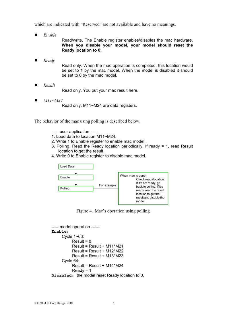
3.2.1. MAC using Polling Address Read access Write access macBase Enable Enable macBase+ 0x04 Ready Reserved macBase + 0x08 Reserved Reserved macBase + 0x0C Result Reserved macBase + 0x10 Reserved M11 macBase + 0x14 Reserved M12 macBase + 0x18 Reserved M13 macBase + 0x1C Reserved M14 macBase + 0x20 Reserved M21 macBase + 0x24 Reserved M22 macBase + 0x28 Reserved M23 macBase + 0x2C Reserved M24 macBase + 0x30 Reserved Reserved
Table 1. Memory map for the control registers of the MAC hardware model using polling. The macBase is defined as 0x0C000064. Each address location in the memory space has two meanings, one for read access, and the other for write access. The meaning of each register is listed below, accesses
IEE 5004 IP Core Design, 2002 5
which are indicated with “Reserved” are not available and have no meanings. Enable
Read/write. The Enable register enables/disables the mac hardware. When you disable your model, your model should reset the Ready location to 0.
Ready Read only. When the mac operation is completed, this location would be set to 1 by the mac model. When the model is disabled it should be set to 0 by the mac model.
Result
Read only. You put your mac result here.
M11~M24 Read only. M11~M24 are data registers.
The behavior of the mac using polling is described below.
----- user application ------ 1. Load data to location M11~M24. 2. Write 1 to Enable register to enable mac model. 3. Polling. Read the Ready location periodically. If ready = 1, read Result
location to get the result. 4. Write 0 to Enable register to disable mac model.
When mac is done:Check ready location. If it's not ready, go back to polling. If it's ready, read the result location to get the result and disable the model.
Load Data
Enable
PollingFor example
Figure 4. Mac’s operation using polling.
----- model operation ------ Enable:
Cycle 1~63: Result = 0 Result = Result + M11*M21 Result = Result + M12*M22 Result = Result + M13*M23
Cycle 64: Result = Result + M14*M24 Ready = 1
Disabled: the model reset Ready location to 0.

IEE 5004 IP Core Design, 2002 6
3.2.2. MAC using Interrupt The memory map and behavior of interrupt method MAC is described below:
Address Read access Write access macBase Enable Enable macBase+ 0x04 Reserved Reserved macBase + 0x08 Reserved Clear macBase + 0x0C Result Reserved macBase + 0x10 Reserved M11 macBase + 0x14 Reserved M12 macBase + 0x18 Reserved M13 macBase + 0x1C Reserved M14 macBase + 0x20 Reserved M21 macBase + 0x24 Reserved M22 macBase + 0x28 Reserved M23 macBase + 0x2C Reserved M24 macBase + 0x30 Reserved Reserved
Table 2. Memory map for the control registers of the MAC hardware model using interrupt. The macBase is defined as 0x0C000064. The meanings of each registers are explained below: Enable
Read/write. The Enable register enables/disables the mac hardware. When you disable your model, your model should reset the Ready location to 0.
Clear
Write only. Writing to the Clear location clears an interrupt generated by the counter timer.
Result Read only. You put your mac result here.
M11~M24
Read only. M11~M24 are data registers.

IEE 5004 IP Core Design, 2002 7
The behavior of the mac using interrupt is described below.
----- user application ------ 1. Install interrupt handler. 2. Enable IRQ. 3. Load data to location M11~M24. 4. Write 1 to Enable register to enable mac model. 5. Continue. Do any operations as you want.
When mac is done:1. Mac set IRQ=1.2. ARM processor jumps to IRQ handler. And after the service in IRQ handler is done, ARM jumps back to useapplication.
In IRQ handler:1. Clear IRQ2. Read result3. Disable mac
Install interrupt handler
Enable IRQ
Load Data
Enable
ContinueWhat happens
Figure 5. Mac’s operation using interrupt.
----- model operation ------ Cycle 1~63:
Result = 0 Result = Result + M11*M21 Result = Result + M12*M22 Result = Result + M13*M23
Cycle 64: Result = Result + M14*M24 IRQ = 1
3.3. Lab Steps
1. Copy the build directory mac.b from C:\ARMSoC\Lab_06\Part1\ to install_directory\ARMulate \armulext\mac.b 2. Modify the make file Makefile in intall_directory\ARMulate\armulext\mac.b\ intelrel\ to suit your path. The default settings will work with the example fine. 3. Open a command console, change the path to intall_directory\ARMulate\armulext\ mac.b\intelrel\, type “nmake” to build mac.dll 4. Copy mac.dll from intall_directory\ARMulate\armulext\mac.b\intelrel\ to the
install_directory\bin. This is where ARMulator finds the DLLs in this directory.
IEE 5004 IP Core Design, 2002 8
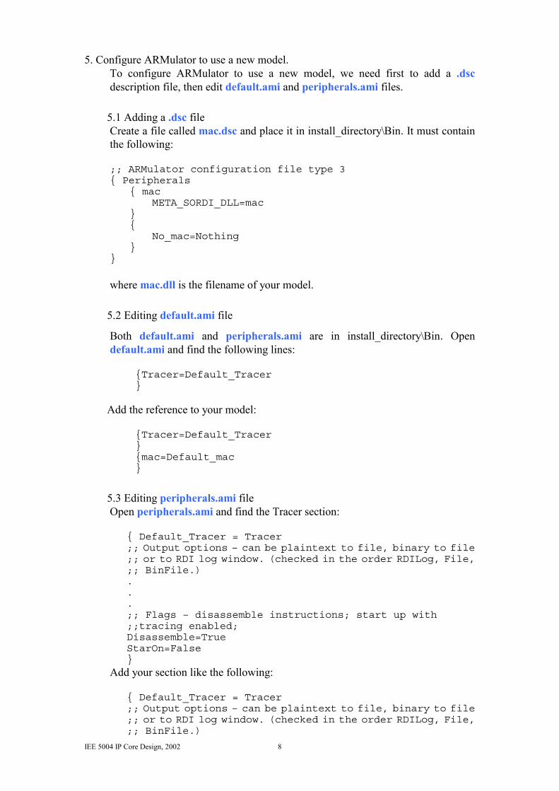
5. Configure ARMulator to use a new model. To configure ARMulator to use a new model, we need first to add a .dsc description file, then edit default.ami and peripherals.ami files.
5.1 Adding a .dsc file Create a file called mac.dsc and place it in install_directory\Bin. It must contain the following: ;; ARMulator configuration file type 3 { Peripherals { mac META_SORDI_DLL=mac } { No_mac=Nothing } } where mac.dll is the filename of your model.
5.2 Editing default.ami file
Both default.ami and peripherals.ami are in install_directory\Bin. Open default.ami and find the following lines:
{Tracer=Default_Tracer }
Add the reference to your model:
{Tracer=Default_Tracer } {mac=Default_mac }
5.3 Editing peripherals.ami file Open peripherals.ami and find the Tracer section:
{ Default_Tracer = Tracer ;; Output options – can be plaintext to file, binary to file ;; or to RDI log window. (checked in the order RDILog, File, ;; BinFile.) . . . ;; Flags – disassemble instructions; start up with ;;tracing enabled; Disassemble=True StarOn=False }
Add your section like the following:
{ Default_Tracer = Tracer ;; Output options – can be plaintext to file, binary to file ;; or to RDI log window. (checked in the order RDILog, File, ;; BinFile.)

IEE 5004 IP Core Design, 2002 9
.
.
. ;; Flags – disassemble instructions; start up with ;;tracing enabled; Disassemble=True StarOn=False } { Default_mac = mac }
6. Verifying a new model. Verifying the MAC hardware model requires the following steps:
6.1 Write a code using the MAC hardware model. In this lab, the main code using polling is provided in ARMSoC\Lab_06\Part1\mac_poll\mac_poll_test.c; the main code using interrupt is provided in ARMSoC\Lab_06\mac2\Part1\ mac_int_test.c.
6.2 Use CodeWarrior to manage your project and build the test program. The project files for MAC using interrupt and polling are provided in ARMSoC\
Lab_06\Part1\mac_int\mac_int_test.mcp and \mac_poll\mac_poll_test.mcp respectively.
6.3 Run AXD and check the results and see if your model operates correctly.

IEE 5004 IP Core Design, 2002 10
4. PART II: Prototyping with Logic Module
4.1. Introduction While designing an IP, it is important to make sure the design could work as part of the system. The simplest and the most direct way is to port our design to an FPGA and verify the results. Note that prototyping using FPGA cannot be done before the designer starts the HDL hardware design procedure, therefore the designer can only verify the design after the design’s HDL coding has been completed. Yet using virtual prototyping, the designer would have more design space to explore. It allows the designer to know how their IP might work with the system, and know their options and limitations more before detailed architectural design, especially from the system’s point of view. ARM Integrator’s Logic Module can work alone like most FPGA development board provided by ALTERA or XILINX. Still it can also be attached to ARM Integrator’s Application Platform and operates with Core Module together. This configuration provides a complete system which represents as a basic platform model in SOC design.
4.2. Basics and Work Flow for Prototyping with Logic Module
4.2.1. Introduction to Logic Module LM-XCV600E+ ARM Logic Module (LM) provides a platform for developing Advanced Microcontroller Bus Architecture (AMBA), Advanced High-performance Bus (AHB) and Advanced Peripheral Bus (APB), and peripherals for the use with ARM-based system. The LM can be used as a standalone system like an FPGA test board, or used with a Core Module (CM) and an Application Platform (AP). It can also work as a CM with AP if a synthesized ARM core is programmed into the FPGA. The last option is to stack several LMs together without an AP motherboard if one of the LMs provides the system controller functions of a motherboard. The LM contains several components as shown in Figure 6. An LM has an ALTERA or XILINX FPGA, our LM uses XILINX FPGA. It has a configuration PLD and a flash memory for storing FPGA configurations. A 1MB ZBT SSRAM is provided for local storage. There’s a prototyping grid where the user can attach small circuits to LM. The system bus connector provides connection to AP motherboard or to other modules. The LM also incorporates with several peripherals such as LEDs, user-definable push button and switches. The layout of the LM is illustrated in Figure 7. Please refer to “Integrator/LM-XCV600E+ User Guide” for further architecture details.

IEE 5004 IP Core Design, 2002 11
Figure 6. The architecture of a Logic Module.
Figure 7. Logic Module’s board layout.
The LM can be linked with JTAG, Trace, or logic analyzer connectors. There is a configuration mode, which changes the JTAG signal routing and is used to download new PLD or FPGA configurations.

IEE 5004 IP Core Design, 2002 12
4.2.2. FPGA tools FPGA Compiler II (FCII) is a GUI synthesis tool for Xilinx FPGA. Figure 8 illustrates the general synthesis flow for using FCII. The HDL design is imported into the GUI synthesis tool, and the synthesis tool generates the EDIF netlist. Then the batch script provided by Xilinx will perform place and route to generate the FPGA binary bit data the EDIF netlist as input. The FPGA binary bit data is used to program the FPGA on the LM.
Figure 8. Xilinx FPGA synthesis flow.
4.2.3. Steps for synthesizing with FPGA Compiler II: Example1 0. Extract v2000e.zip to %xilinx%\virtexe\data\ 1. Start Xilinx Foundation from the start menu.
Figure 9. Starting Xinlinx FPGA CompilerII’s from the Start-Uup menu. 2. Execute the Project Manager of Xilinx Foundation 3. Create a New Project
–Input Name (assume: example1) –Flow: HDL

IEE 5004 IP Core Design, 2002 13
Figure 10. Getting Started window in Project Manager.
Figure 11. New Project setting window.
4. Project → add source File(s) (c:\ARMSoC\Lab_06\Part1I\example1\ example1.v)
–Analyzing…
Figure 12. Add Source File(s) to the Project.

IEE 5004 IP Core Design, 2002 14
5. Synthesis → synthesize.. –Top level –Target device
•Family: VirtexE •Device: v2000efg680 •Speed: -6
–Run and create example1.edf
Figure 13. Synthesize the design.
Figure 14. The Synthesis/Implementation settings window.
4.2.4. Running Xilinx Place and Route Batch Scripts 1. cd c:\ARMSoC\lab_06\example1\ 2. copy %xilinx%\active\projects\example1\example1.edf 3. replace all ‘<’ ‘>’ with ‘(’ ‘)’ of example1.edf with UltraEdit or any other editor 4. replace the ‘filename’ of c:\ARMSoC\lab_06\example1\pc_par.bat with example1 5. execute pc_par.bat to generate example1.bit

IEE 5004 IP Core Design, 2002 15
4.2.5. Downloading the Binary Bitstreams 1. Open the download setting files c:\ARMSoC\lab_06\example1\ example1_to_flash.brd and example1_to_fpga.brd. These two files are shown in Figure 15 and Figure 16.
Figure 15. Example1_to_fpga.brd
Figure 16. Example1_to_flash0.brd
Modify the content of example1_to_fpga.brd and example1_to_flash.brd as shown in Figure 15 and Figure 16. Remove Step2Address = 200000 or Step3Address = 200000 if possible.(#Address 0x200000 saves the test image of LM, avoid modifying image 1 at 0x200000)
[General] Name = example1 XCV2000E -> fpga Priority = 1 [ScanChain] TAPs = 2 TAP0 = XCV2000E TAP1 = XC9572XL [Program] SequenceLength = 1 Step1Method = Virtex Step1TAP = 0 Step1File = example1.bit
[General] Name = example1 XCV2000E -> flash (addr 0x0) Priority = 1 [ScanChain] TAPs = 2 TAP0 = XCV2000E TAP1 = XC9572XL [Program] SequenceLength = 3 Step1Method = Virtex Step1TAP = 0 Step1File = lmxcv600e_72c_xcv2000e_via_reva_build0.bitStep2Method = IntelFlash Step2TAP = 0 Step2File = example1.bit Step3Method = IntelFlashVerify Step3TAP = 0 Step3File = example1.bit

IEE 5004 IP Core Design, 2002 16
2. Connect ARM MultiICE onto LM (Be SURE to power down first!! …$$) 3. Set the LM in Config Mode by pushing the CFGLNK button on the front side of the development system’s case. The CFGLED on the LM is lit as an indication that the configure mode is selected. 4. Auto-config again in the MultiICE Server program. Remember to auto-config again each time the MultiICE link is modified. 5. Execute progcards.exe to download the bitstream to the FPGA. This download program only searches for the .brd files in the same directory. If only one .brd file exists, the downloading would start directly without any prompt.
4.2.6. Running the Downloaded Bitstream from FPGA 1. Execute progcards.exe and select example1 XCV2000E->fpga. 2. This will take about 1 minute. It’s a Plug-and-Play version.
4.2.7. Running the Downloaded Bitstream from Flash(0x00) 1. Execute progcards.exe and select example1 XCV2000E->flash(addr 0x00). 2. This will take about 3 minutes. Remove the CONFIG link after downloading. 3. Power down the LM. 4. Select the flash image to be executed. Which flash image to be executed is selected by the position of the 4-way switch S1 on the LM. It is only active in power-up blink. Consult Table 3 and change the position of S1 while in stand-by mode. The circled positions are better than the crossed ones because of being independent of CFGSEL[1:0].
Table 3. The relation between the 4-way switch positions and the selected flash image. 5. Power the LM up again and observe the LM. You will see the LEDs on the LM flashing from left to right. The combination of the switch S1 can changed the flashing frequency.

IEE 5004 IP Core Design, 2002 17
4.2.8. A Timing Information Example Figure 17 shows the distribution of each stage during the FPGA working flow. The proportion of total execution time of each stage is also shown in this figure. As can be seen, place-and-route using the batch scripts occupies 50% of the total execution time. Therefore we strongly suggest users to perform place-and-route on a faster PC, since it’s the most time-consuming work.
Figure 17. The execution time distribution of each stage in the FPGA working
flow.
4.3. Working Hardware and Software Together: Example 2
4.3.1. About Example 2 This example will perform the following tasks:
1. Determines DRAM size on the core module and sets up the system controller 2. Checks that the logic module is present in the AP expansion position 3. Reports module information 4. Sets the logic module clock frequencies 5. Tests SSRAM for word, halfword, and byte accesses. 6. Flashes the LEDs 7. Remains in a loop that displays the switch value of the LM on its LEDs
The task to show the switch value with the LEDs is done by the simple hardware design programmed into the FPGA on LM.

IEE 5004 IP Core Design, 2002 18
4.3.2. Basic Platforms: AHB and ASB The example contains two versions of implementation which support the following two configurations: AHB MB and AHB peripherals ASB MB and AHB peripherals
Figure 18 supports the first configuration, and Figure 19 supports the second one.
Figure 18. Implementation the support AHB system.
Figure 19. Implementation that supports ASB system.
The alphanumerical LED display on the Integrator AP motherboard can show whether it is AHB or ASB. The letter shown corresponds to either of the two systems, which will be shown below: H: AHB S: ASB
In this course, our configuration is illustrated in Figure 20. The blocks inside the dashed bounding box represent the architecture to be programmed into the LM’s FPGA.

IEE 5004 IP Core Design, 2002 19
Figure 20. The AHB platform and its block diagram used in this course.
4.3.3. HDL Files Descriptions Each block in the LM is described with an HDL design file. The description of each HDL files is provided in Table 4.
File Description
ASBAHBTop AHBAHBTop
These files are the top-level HDL that instantiate all of the high-speed peripherals, decoder, and all necessary support and glue logic to make a working system. The files are named so that, for example, ASBAHBTop.vhd is the top level for AHB peripherals connected to an ASB system bus.
ASB2AHB This is the bridge required to connect AHB peripherals to an ASB Integrator system.
AHBDecoder
The decoder block provides the high-speed peripherals with select lines.These are generated from the address lines and the module ID (position in stack) signals from the motherboard. The decoder blocks also contain the default slave peripheral to simplify the example structure. The Integrator family of boards uses a distributed address decoding system
AHBMuxS2M This is the AHB multiplexor that connects the read data buses from all of the slaves to the AHB master(s).
AHBZBTRAM High-speed peripherals require that SSRAM controller block supports word, halfword, and byte operations to the SSRAM on the logic module.
AHB2APB This is the bridge blocks required to connect APB peripherals the the high-speed AMBA AHB bus. They produce the peripheral select signals for each of the APB peripherals.
AHBAPBSys
The components required for an APB system are instantiated in this block. These include the bridge and the APB peripherals. This file also multiplexes the APB peripheral read buses and concatenates the interrupt sources to feed into the interrupt controller peripheral.
APBRegs
The AOB register peripheral provides memory mapped registers that you can use to:
Configure the two clock generators Write to the user LEDs Read the user switch inputs.
It also latches the pressing of the push button to generate an expansion interrupt.

IEE 5004 IP Core Design, 2002 20
APBIntcon The APB interrupt controller contains all of the standard interrupt controller registers and has an input port for four APB interrupts. Four software interrupts are implemented.
Table 4. The description of each HDL file.
4.3.4. Software File Descriptions There are four software files in this example. The description of each software file is provided in Table 5.
File Description
Logic.c
These files are the top-level HDL that instantiate all of the high-speed peripherals, decoder, and all necessary support and glue logic to make a working system. The files are named so that, for example, ASBAHBTop.vhd is the top level for AHB peripherals connected to an ASB system bus.
Logic.h This is the bridge required to connect AHB peripherals to an ASB Integrator system.
Platform.h
The decoder block provides the high-speed peripherals with select lines. These are generated from the address lines and the module ID (position in stack) signals from the motherboard. The decoder blocks also contain the default slave peripheral to simplify the example structure. The Integrator family of boards uses a distributed address decoding system
Rw_support.s This is the AHB multiplexor that connects the read data buses from all of the slaves to the AHB master(s).
Table 5. The description for each software file.
4.3.5. Logic Module Registers The memory space within a LM and its relation with Integrator’s system memory space is illustrated in Figure 21. The description of each LM registers is described in Table 6. The offset address represents the register’s offset from the base address.
Figure 21. Relations between LM’s memory space and the Integrator system’s memory space

IEE 5004 IP Core Design, 2002 21
Table 6. Register map of an LM.
Table 7. Push button interrupt register.
4.3.6. Interrupt Controller The interrupt controller in LM manages the IRQs from the user’s design and the peripheral devices on LM. The Integrator system treats the LM as a single slave device, therefore there’s only one IRQ signal connected from LM to the motherboard. Figure 22 shows the basic bit-slice structure of the interrupt controller. The Set-Clear register and the “AND” gate can perform interrupt enable masking, so that only the enabled interrupt requests are allowed. The corresponding control registers for interrupt controller are listed in Table 8.
Figure 22. Bit-slice of LM’s interrupt controller’s structure.

IEE 5004 IP Core Design, 2002 22
Table 8. Interrupt controller’s registers.
4.3.7. Running of Example 2 0. Execute c:\ARMSoC\lab_06\Part1I\example2\runme.bat at the first time. It would copy the new .brd to the proper location. 1. Check the LM and be sure that the flash image of AHB subsystem (example2 AHB
XCV2000E -> flash (addr 0x0), not addr 0x200000!!) has been configured and the switch has been on the right position to select the correct flash image. (refer to the steps in 4.2.7)
2. Connect the Multi-ICE onto CM (Be SURE under the stand-by mode!!)…$$ 3. Start Multi-ICE server program and press Auto-Configure. 4. Execute the CodeWarrior. 5. Choose Open from the tool panel (or press Ctrl + O).
Table 9. Open icon in the CodeWarriorIDE.

IEE 5004 IP Core Design, 2002 23
6. Choose C:\ARMSoC\Lab_06\Part1I\example2\sw\sw.mcp
Figure 23. Open the project file.
7. Convert Project.
Figure 24. Convert Project window.
8. Make the project
Figure 25. Press the Make button on the Project window.
9. After make completion, check the make report. 0 error and 1 warning is ok.
Figure 26. Errors & Warnings window after making the project.
IEE 5004 IP Core Design, 2002 24
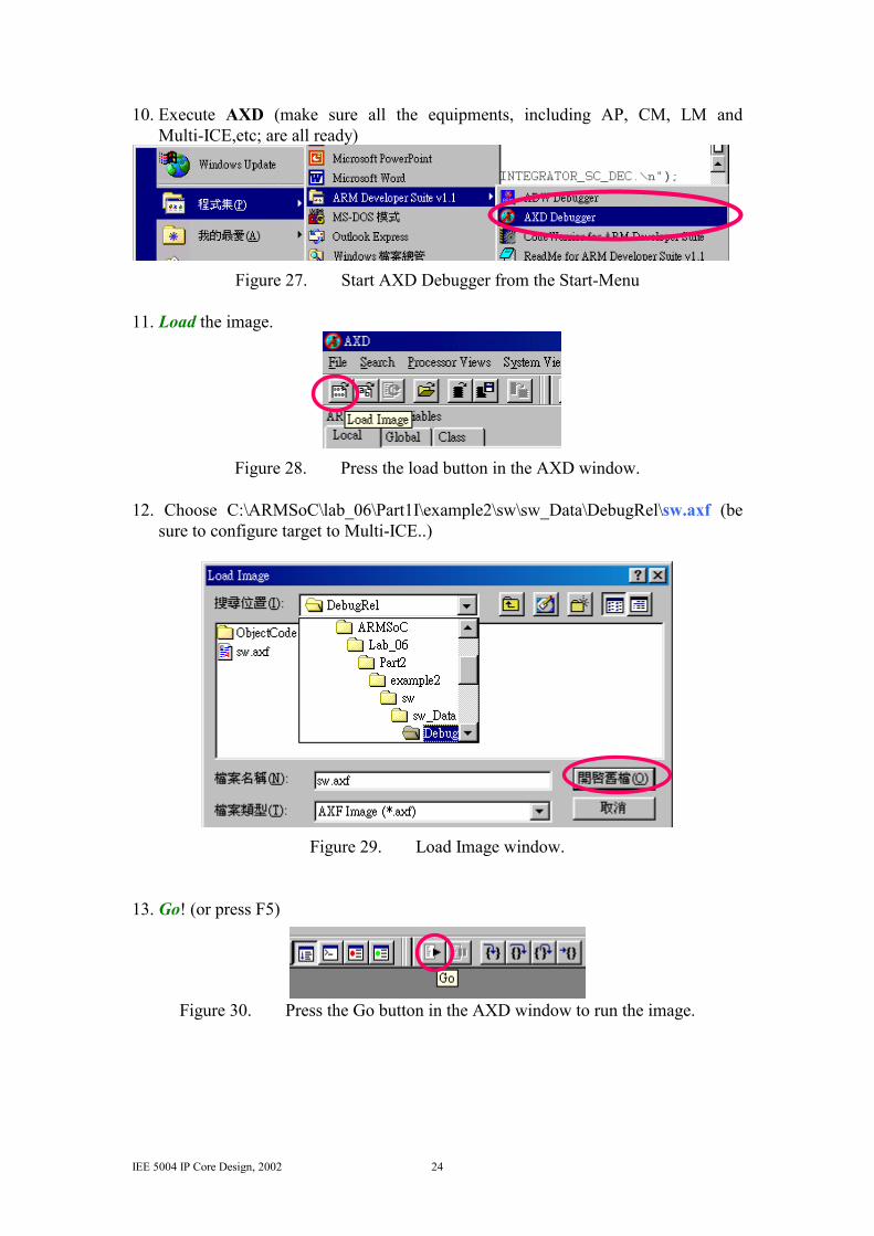
10. Execute AXD (make sure all the equipments, including AP, CM, LM and
Multi-ICE,etc; are all ready)
Figure 27. Start AXD Debugger from the Start-Menu
11. Load the image.
Figure 28. Press the load button in the AXD window.
12. Choose C:\ARMSoC\lab_06\Part1I\example2\sw\sw_Data\DebugRel\sw.axf (be
sure to configure target to Multi-ICE..)
Figure 29. Load Image window.
13. Go! (or press F5)
Figure 30. Press the Go button in the AXD window to run the image.
IEE 5004 IP Core Design, 2002 25
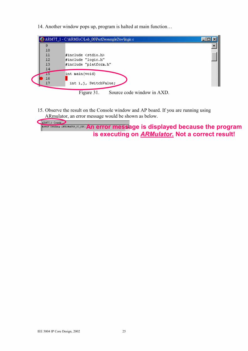
14. Another window pops up, program is halted at main function…
Figure 31. Source code window in AXD.
15. Observe the result on the Console window and AP board. If you are running using
ARmulator, an error message would be shown as below.
An error message is displayed because the programis executing on ARMulator. Not a correct result!

IEE 5004 IP Core Design, 2002 26
5. Exercise: an RGB-to-YUV program Design an RGB-to-YUV converting hardware module that converts R, G, B values into Y, U, V values: 1. Implement the converter with pure software; you’ll need to write the test program. 2. Implement the converter into hardware and program it into the FPGA on the LM,
evaluate the improvement compared to pure software implementation. Hint: you may modify AHBAHBTop.v, AHBDecoder.v, AHBMuxS2M.v,
and AHBZBTram.v in example 2.
Figure 32 RGB to YUV transfer function.