journal of computational science
TRANSCRIPT

I
MWP
a
ARRAA
KNDcOPP
1
mtdpuipmdotsi
daoda
e((p
1h
Journal of Computational Science 4 (2013) 313–324
Contents lists available at ScienceDirect
Journal of Computational Science
journa l h om epage: www.elsev ier .com/ locate / jocs
mproving the design cycle for nanophotonic components
artin Fiers ∗, Emmanuel Lambert, Shibnath Pathak, Bjorn Maes, Peter Bienstman,im Bogaerts, Pieter Dumon
hotonics Research Group (INTEC), Ghent University – IMEC, Sint-Pietersnieuwstraat 41, B-9000 Ghent, Belgium
r t i c l e i n f o
rticle history:eceived 24 February 2011eceived in revised form 17 February 2013ccepted 17 May 2013vailable online 5 June 2013
a b s t r a c t
We present IPKISS, a software framework that greatly simplifies the design of nanophotonic components.In this approach, all steps in the workflow are based on a single high-level definition of the component,in a Python script. Because there is only one description, the design flow becomes less error prone dueto incorrect definitions, and the overall reproducibility is greatly improved.
Furthermore it enables easy closed-loop modeling of components and circuits. Also, previous workcan easily be built upon because lower level blocks can seamlessly be replaced by new blocks. While we
eywords:anophotonicsesigning and modeling opticalomponentsptical circuit design
illustrate the application in photonics, this software and the used design patterns can be extended toother domains such as RF design and to multidomain physics such as opto-electronics.
© 2013 Elsevier B.V. All rights reserved.
arametrized cellython
. Introduction
In a typical research or design environment, fabrication oficro-and nanoscale devices is an expensive process with long
urnaround times. Prior to submitting a design for fabrication, theseevices are typically modeled and simulated in software. For exam-le, in the field of nanophotonics, electromagnetic simulations aresed to calculate how light propagates through such a device. Often
t is also required to perform tolerance analysis on the designarameters as well as on effects of the fabrication process. Oneajor difficulty that arises when designing these devices is that the
ifferent simulation tools have their own user interface and more-ver have their own representation to define components. Defininghese devices in different tools is a laborious job, and there is a con-iderable risk of introducing errors in the specification of the devicen each tool.
The main characteristic of our approach is that a component isefined only once on a high level [1]. This component is available as
parametrized cell (PCell), a concept originating from the design
f electronic circuits. Then, the necessary representations (e.g. aiscretized matrix representing the component, a cross-section,list of polygons, port positions) to drive the different tools
∗ Corresponding author. Tel.: +32 92643272.E-mail addresses: [email protected], [email protected] (M. Fiers),
[email protected] (E. Lambert), [email protected]. Pathak), [email protected] (B. Maes), [email protected]. Bienstman), [email protected] (W. Bogaerts),[email protected] (P. Dumon).
877-7503/$ – see front matter © 2013 Elsevier B.V. All rights reserved.ttp://dx.doi.org/10.1016/j.jocs.2013.05.008
(simulation, visualization, routing) are extracted from this defi-nition. The transition to different simulation tools should only bewritten once in a generic way, which makes simulations much lesserror prone. It is also much easier to reproduce earlier results andto change sub-parts of the design. In this way, many variationscan easily be compared to one another (e.g. a different simulationmethod, an improved component, or a modified design).
Python is our programming language of choice. The main rea-son for using this programming language is the flexibility which itoffers: it can be used to make very complex software designs, yetit has a relatively low threshold for researchers without extensiveprogramming skills. Our software toolset revolves around a cen-tral design framework called IPKISS [1], which can interface withdifferent in-house and third-party simulation tools.
The paper is structured as follows: as the reader might notbe familiar with photonics, we very briefly describe this specificresearch field in Section 2. In Section 3, we illustrate a typical work-flow, i.e. the steps needed to design a nanophotonic component. Weshow which design problems typically arise and demonstrate howthe software framework improves this flow. In Section 4, the tech-nical design and implementation of the framework is described,and in the fifth section we illustrate how we use the software toefficiently design a complex optical component: An Arrayed Wave-guide Grating. We conclude by providing license information. Aspreviously noted, it is easy to extend this architecture beyond the
horizon of photonics: electronic design, multidomain physics andso on. Throughout the paper, we use Python code to explain sev-eral core concepts. The code aims to be descriptive rather than toexplain all details.
314 M. Fiers et al. / Journal of Computational Science 4 (2013) 313–324
F integs ide tof
2
tccrroTppeciFrSIufm
iihlaw
mttat
3
(
ig. 1. Some examples of nanophotonic subcomponents, used for designing smallometimes needed. Tapers (right) are used to spread light from a narrow waveguabricated devices are shown.
. Photonics
Photonics is the field of manipulating, generating and detec-ing light (photons) by means of optical components. This is inontrast to electronics, in which electrons are the informationarriers. Some examples of photonic devices are: lasers, opticaleceivers and transmitters, CD/DVD drives and LED lighting. Aecent trend in photonics is the drive towards miniaturizationf components, and integrating many of them on a single chip.hese so-called (nano)photonic integrated circuits have a bettererformance, are more robust, and consume less power than bulkhotonics, low-contrast integrated photonics and electronics. Onexcellent material for making such optical chips is silicon. Sili-on has very low absorption losses in the wavelength range thats used for fibre-optic communications (1300 nm and 1550 nm).ortunately, silicon is already widely used in electronic chip fab-ication, so we can reuse standard Complementary Metal Oxideemiconductor (CMOS) technology to manufacture photonic chips.n this technology, the silicon on insulator (SOI) wafer is patternedsing deep UV lithography [2]. This opens the door to wafer-scaleabrication of nanophotonic chips, leading to devices that can be
anufactured in large volumes at low cost.A few subcomponents of a nanophotonic circuit are displayed
n Fig. 1. The resulting device consists of submicrometer wide sil-con lines on top of a thick glass layer. Because silicon has a veryigh index of refraction, the submicron line acts as a waveguide for
ight: electromagnetic waves with wavelengths between 1.3 �mnd 1.55 �m can travel along the line (a so-called “photonic wire”)ithout much loss.
By optimizing the geometry of the silicon, the light can beanipulated. Fig. 1(a, c) shows a crossing of two waveguides, where
he geometry is engineered such that there is no crosstalk betweenhe waveguides. In Fig. 1(b, d) we change the width of the siliconround the core of the waveguide and then stop the waveguide, sohat light can diffract in the thin layer of silicon on the chip.
. Workflow for designing a component
To illustrate the problems associated with a manual workflowthat is, before adopting the framework), as well as the innovation
rated optical circuits. Because a nanophotonic circuit is planar, crossings (left) are a broad one. On the bottom, Scanning Electron Microscope (SEM) pictures of the
brought by our framework, we will discuss the workflow for design-ing a typical photonic integrated component: a multimode interfer-ometer (MMI). Although we use an optical component to illustratethe workflow, readers from other research domains might identifythe same or similar problems based on their own experience.
In Section 3.1 we briefly introduce this device and its typicaldesign steps. We show that in the classical workflow (3.2) thereare a lot of manual interactions, leading to a slow, and more impor-tantly an error-prone workflow. A workflow based on our software(3.3) shows how one can circumvent these problems.
3.1. Example device: MMI
We will illustrate our workflow using a device that splits thelight in a waveguide into two equal parts, an important buildingblock in photonic IC design. It is called a multimode interferometer(MMI), and is depicted in Fig. 2. This example is representative tomany photonic design problems and is practiced by most photonicdesigners today, irrespective of the specific tools they use in eachstep of the problem. The MMI consists of a sequence of waveguideelements of different widths and shapes. Each waveguide supportsa number of electromagnetic waveguide modes, i.e. eigensolutionsof the light distribution in the dielectric medium.
There are several aspects to modeling this device, which areillustrated in Fig. 2. When exciting the MMI with a mode in an inputwaveguide, one needs to know the shape (spatial distribution) ofthis mode, called the mode profile. We calculate this waveguidemode profile using an eigenmode solver (Fig. 2, top left). The modehas a gaussian-like profile, as shown in the figure. The mode profileis then entered as input for a full-wave time-domain simulation tocalculate the light propagation in the device (Fig. 2, top right). Asthree-dimensional (3D) full-wave simulations are computationallyvery intensive, one will first run an approximate simulation in 2Dusing well-known approximation methods and only then run full3D simulations.
In order to get a highly accurate representation of the device
characteristics, a 3D simulation is then performed. From this sim-ulation, the scatter matrix is extracted, leading to a high-leveldescription of the building block. In a circuit simulation tool (Fig. 2,bottom right), several of these building blocks are combined, in
M. Fiers et al. / Journal of Computational Science 4 (2013) 313–324 315
Fig. 2. Combining several simulation tools when designing a nanophotonic light splitter. Top left: an eigenmode solver (e.g. CAMFR [3]) which calculates the mode profile ofa e domi , usersi
oTto
wm
h
3
ospdFFa
3
Wtglsbbs
waveguide (a gaussian-like shape), which is used as input for a finite difference tims then sent to a circuit simulation tool (e.g. Caphe [19], [20]), see bottom right. Alson Python.
rder to create functional devices (for example optical filters).hese simulations run much faster, and more attention is given tohe phenomenological parameters, rather than the physical layoutf the actual device.
In addition, most designers will want to integrate a piece of own-ritten code (for example a numerical algorithm or an analyticalodel) in the design flow as well (Fig. 2, bottom left).Below we give a description of the specific simulation tools we
ave used:
.1.1. Eigenmode solvers: CAMFR [3] and Fimmwave [6]CAMFR is written in C++with a Python interface. It is devel-
ped at Ghent University and can be downloaded for free. Theource is being distributed under a dual license scheme (GPL androprietary) [4]. The software is used to calculate modes in a one-imensional approximation of the geometry, for a fast simulation.or accurate simulations, we use the commercial software toolimmwave (Photon Design) to simulate the eigenmodes in thectual two-dimensional cross-section.
.1.2. Full-wave time domain simulation: Meep FDTD (MIT) [5]Meep is an open-source finite difference time domain simulator.
ith this tool, the fields are calculated at all positions and at allimes. It is used either in 2D approximation or in full 3D. Making a
eometry in Meep is usually done using the Scheme programminganguage. Although very powerful, experience learns that it takesome iterations before the device is represented correctly if it has toe defined manually. For devices with complex geometries, this cane a tedious job. Also, importing modes from an electromagneticimulator is a laborious and error-prone job.ain (FDTD) simulation (e.g. Meep [5]) on the top right. The output of this simulation might want to perform a part of the simulation using their own code (bottom left)
3.1.3. Circuit simulation: Caphe [19,20]We use an in-house developed circuit simulator Caphe to
simulate optical circuits. The extracted results of the full-wavesimulations (for example a scatter matrix S) for each device areimported in Caphe, which can then calculate the time and frequencyresponse of the full circuit.
3.2. Classical workflow
From the example above, it is clear that a lot of manual actionsare required to successfully model an optical component, and evenmore to model a circuit. In the classical workflow, one manuallycommunicates information from one tool to the other tool. One ofthe key issues here is that it is rather tedious as well as error-proneto exchange information between these tools: the output of differ-ent tools usually have different file formats and/or the way this datais loaded into the simulation is different. In some cases, one evenhas to write different scripts for one tool, for instance for runningthe 2D and 3D simulations in Meep. Also, data is gathered in differ-ent formats and post-processed in various external environmentssuch as Excel and Matlab, which involves a lot of manual data con-version for each tool. Use of the different tools requires learningnew graphical and scripting or programming interfaces over andover again.
3.3. New workflow
The new workflow that we developed in the past years andwhich we use for our own work, is much more automated than theworkflow described previously which involved manual importingand exporting of results, and redefining components. It is based on

316 M. Fiers et al. / Journal of Computational Science 4 (2013) 313–324
Fig. 3. Integrated workflow for designing a multimode interferometer (MMI). There is only one high-level description of the component, and all other steps extract informationf progre iteratim
asl
12
3456
off
Ltr
adfcamplfsi
rom this description. For example, the simulation is performed without additional
liminated. The reproducibility is greatly improved, and the designer can focus on
anually in different simulation tools.
single representation of the component in a high-level Pythoncript. The workflow is depicted in Fig. 3 and incorporates the fol-owing steps:
. Component definition
. Virtual fabrication, generating the simulation geometry andvisualization
. Simulation
. Data processing
. Re-iterate previous steps where needed
. Generate the final layout for fabrication
1. Component definition. Users can write their own libraryf components on top of IPKISS. The multimode interferometerrom Fig. 2 is part of such a library and can be instantiated asollowing:
isting 3.3.1. Creation of the component (see also Listing 4.1.1 forhe class definition). Keyword arguments are required, to improveeadability of the code.
mmi = MmiSimple(lengt h=10. 0, widt h=5. 0)
2. Virtual fabrication, generating the simulation geometry and visu-lization. The physical description of the component is typicallyone through a geometric representation of the photomasks usedor the fabrication of the devices: the devices are fabricated in semi-onductor using a series of lithography and etching steps (see [2]),nd at each lithography step a geometric mask is projected onto theaterial. At design time, the final geometry of the fabricated com-
onent is therefore represented as a list of polygons on each mask
ayer. This can be exported to a number of common image formatsor quick inspection. The simulation geometry for electromagneticimulations is automatically generated from the mask layout. Thiss done through a virtual fabrication routine which performs anamming work, so errors when describing a design for different simulation tools areng through several designs for optimization rather than describing his component
approximation of the actual fabrication process, and operates onthe different mask layers defined in the component layout. Theresulting geometry is a distribution of materials in a 2D or 3D space.Basic design errors can already be corrected here.
In a second step, this internal representation is then convertedto the geometric representation of a specific simulation tool. Thisis illustrated in detail in Section 4.3. Also, from the componentdescription we can extract the positions of the input and outputports, which can be passed to the simulation tool for the correctexcitation and for the correct interpretation.
3. Simulation. A next step involves simulation of the physicalbehavior of the device. As explained in the previous paragraph,the high-level description of the component is used to extract thisgeometry. The interfacing between the different tools is done auto-matically. For example, the mode profile is calculated in CAMFR andthen passed on to Meep, without any additional programming workon the user side. As interfacing to different tools plays a major role inthis framework, we further elaborate on how the actual interfacingis done in Section 4.3, using CAMFR as example.
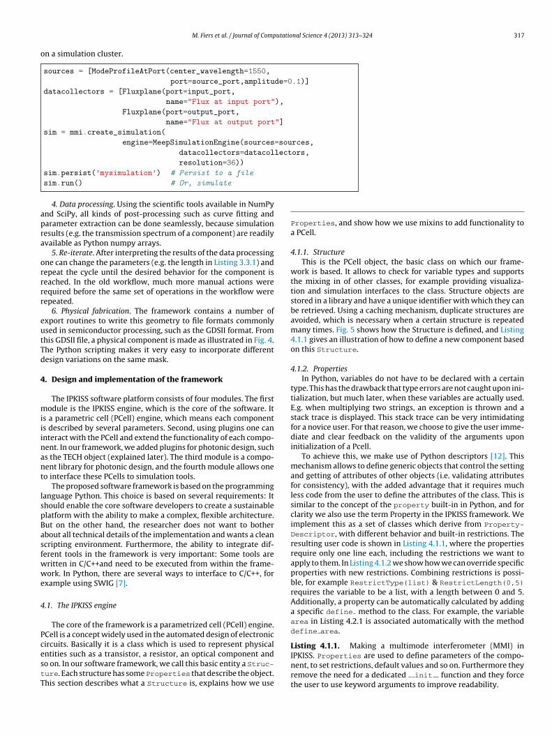
Simulation is an important step in the workflow and usuallyrequires a lot of resources. In the next code example we create asimulation object to perform a simulation with Meep. The high-level design can be persisted to a file (persist) and then executed(run) on a cluster without the user needing to worry about thespecific details on how to run a simulation on a cluster. As explainedbefore, the mode profile is calculated by CAMFR and then used as
input (sources). Detectors are then added (datacollectors).Listing 3.3.2. Defining a simulation for the multimode interferom-eter (MMI). Simulations can be persisted to a file and then executed
utatio
o
de=0
),
"]
=sou
lect
apra
orrrr
eutTd
4
miiinant
lspBasfwwe
4
PcestT
M. Fiers et al. / Journal of Comp
n a simulation cluster.
sources = [ModeProfileAtPort(center_w avel engt h=155 0,
port=source_port,amplitu datacollectors = [Fluxplane(port=input_port,
name="Flu x at inpu t port "
Fluxplane(port=output_port,
name="Flu x at outpu t port sim = mm i.create_simulation (
engine=MeepSimulationEngine(sources
datacollectors=datacol
resolution=36))
sim.persist (’mysimulation ’) # Persis t to a fil e
sim.run( ) # Or , simulat e
4. Data processing. Using the scientific tools available in NumPynd SciPy, all kinds of post-processing such as curve fitting andarameter extraction can be done seamlessly, because simulationesults (e.g. the transmission spectrum of a component) are readilyvailable as Python numpy arrays.
5. Re-iterate. After interpreting the results of the data processingne can change the parameters (e.g. the length in Listing 3.3.1) andepeat the cycle until the desired behavior for the component iseached. In the old workflow, much more manual actions wereequired before the same set of operations in the workflow wereepeated.
6. Physical fabrication. The framework contains a number ofxport routines to write this geometry to file formats commonlysed in semiconductor processing, such as the GDSII format. Fromhis GDSII file, a physical component is made as illustrated in Fig. 4.he Python scripting makes it very easy to incorporate differentesign variations on the same mask.
. Design and implementation of the framework
The IPKISS software platform consists of four modules. The firstodule is the IPKISS engine, which is the core of the software. It
s a parametric cell (PCell) engine, which means each components described by several parameters. Second, using plugins one cannteract with the PCell and extend the functionality of each compo-ent. In our framework, we added plugins for photonic design, suchs the TECH object (explained later). The third module is a compo-ent library for photonic design, and the fourth module allows oneo interface these PCells to simulation tools.
The proposed software framework is based on the programminganguage Python. This choice is based on several requirements: Ithould enable the core software developers to create a sustainablelatform with the ability to make a complex, flexible architecture.ut on the other hand, the researcher does not want to botherbout all technical details of the implementation and wants a cleancripting environment. Furthermore, the ability to integrate dif-erent tools in the framework is very important: Some tools areritten in C/C++and need to be executed from within the frame-ork. In Python, there are several ways to interface to C/C++, for
xample using SWIG [7].
.1. The IPKISS engine
The core of the framework is a parametrized cell (PCell) engine.Cell is a concept widely used in the automated design of electronic
ircuits. Basically it is a class which is used to represent physicalntities such as a transistor, a resistor, an optical component ando on. In our software framework, we call this basic entity a Struc-ure. Each structure has some Properties that describe the object.his section describes what a Structure is, explains how we usenal Science 4 (2013) 313–324 317
.1)]
rces,
ors,
Properties, and show how we use mixins to add functionality toa PCell.
4.1.1. StructureThis is the PCell object, the basic class on which our frame-
work is based. It allows to check for variable types and supportsthe mixing in of other classes, for example providing visualiza-tion and simulation interfaces to the class. Structure objects arestored in a library and have a unique identifier with which they canbe retrieved. Using a caching mechanism, duplicate structures areavoided, which is necessary when a certain structure is repeatedmany times. Fig. 5 shows how the Structure is defined, and Listing4.1.1 gives an illustration of how to define a new component basedon this Structure.
4.1.2. PropertiesIn Python, variables do not have to be declared with a certain
type. This has the drawback that type errors are not caught upon ini-tialization, but much later, when these variables are actually used.E.g. when multiplying two strings, an exception is thrown and astack trace is displayed. This stack trace can be very intimidatingfor a novice user. For that reason, we choose to give the user imme-diate and clear feedback on the validity of the arguments uponinitialization of a Pcell.
To achieve this, we make use of Python descriptors [12]. Thismechanism allows to define generic objects that control the settingand getting of attributes of other objects (i.e. validating attributesfor consistency), with the added advantage that it requires muchless code from the user to define the attributes of the class. This issimilar to the concept of the property built-in in Python, and forclarity we also use the term Property in the IPKISS framework. Weimplement this as a set of classes which derive from Property-Descriptor, with different behavior and built-in restrictions. Theresulting user code is shown in Listing 4.1.1, where the propertiesrequire only one line each, including the restrictions we want toapply to them. In Listing 4.1.2 we show how we can override specificproperties with new restrictions. Combining restrictions is possi-ble, for example RestrictType(list) & RestrictLength(0,5)requires the variable to be a list, with a length between 0 and 5.Additionally, a property can be automatically calculated by addinga specific define method to the class. For example, the variablearea in Listing 4.2.1 is associated automatically with the methoddefine area.
Listing 4.1.1. Making a multimode interferometer (MMI) in
IPKISS. Properties are used to define parameters of the compo-nent, to set restrictions, default values and so on. Furthermore theyremove the need for a dedicated init function and they forcethe user to use keyword arguments to improve readability.
318 M. Fiers et al. / Journal of Computational Science 4 (2013) 313–324
F GDSIIE
MI")
ngle
leng
Lc
stri
eatts
lpTlefiI
Ft
c
ig. 4. Fabricating the multimode interferometer. Left: Exporting the design to the
lectron Microscope (SEM) image of the actual fabricated component.
class MMISimpl e(Structure) :
__name_prefix = "MMISimple "
length=PositiveNumberProperty (def aul t=10. 0)
width=PositiveNumberProperty( defa ult=5.0)
area=PositiveNumberProperty(doc="Area under the M
def define_are a(sel f):
return sel f.widt h*sel f.heigh t
def define_layou t(sel f, layout) :
# Construc t th e MM I usin g rectangle s an d tria
layout+=Rectangle(cente r=(0. 0,0. 0),
box_size=(sel f.width , sel f.
# ad d mor e rectangles , triangles , .. .
...
# Retur n th e layou t
return layou t
isting 4.1.2. Extra restrictions on a Property. The newly createdlass now has a restriction on its length.
class MyMmiSimpl e(MmiSimple) :
length=RestrictedProperty(def aul t=10. 0,
restriction=RESTRICT_NUMBE R & Re
The class StrongPropertyInitializer manages these Prop-rties (see also Fig. 5). It also causes values to be assignedutomatically to the Properties of the PCell, effectively removinghe need for a dedicated init function. Also, the consistency ofhe object can be validated at instantiation. Again, this removes aubstantial amount of user code, improving readability.
In parallel to the development of our PCell class, other powerfulibraries were developed that allow typing of Python variables, sup-ort delegation and initialization of variables. One of these is the
raits library, developed at Enthought [13]. The functionality of thisibrary is very similar to the functionality we provide, and we areven considering of migrating to the Traits library in the future. Therst thing to investigate is the scalability of both libraries, becausePKISS is relatively slow when instantiating a lot of different PCells.
ig. 5. Structure is the basic entity of the IPKISS framework. Other classes can be mixedureCreator, which can analyze the init function and can check for a cached versihecks the consistency of the created object.
format (a format commonly used in semiconductor processing). Right: A Scanning
s
th))
ctRange(3,15))
4.1.3. MixinsThe PCell engine is enriched with new functionality by mixing
additional classes into it. After mixing in a class, the PCell inheritsfrom this class. This is used to add functionality such as generating arepresentation of the physical layout, visualizing, simulations, andinterfacing to external tools, as shown in Fig. 6. There are severalreasons to use mixins rather than to inherit all classes explicitly(multiple inheritance). First of all, it reduces the complexity of the
PCell class. In this way you do not pollute the userspace with func-tionalities that will never be used. Second, new modules can simplybe plugged in without changing the code base. Third, it is a way toprotect intellectual property. Additional functionality can be part ofin using the mixin function. Structure creation is modified using the MetaStruc-
on of the created structure. StrongPropertyInitializer assigns Properties and

M. Fiers et al. / Journal of Computational Science 4 (2013) 313–324 319
F aliz
c own
ai
tc
id
4
4
itwTTgdaocc
Lg
y
ack(
ILIC
ILIC
OLOR
aeeIa
ig. 6. Functionality can be dynamically mixed into the PCell. For instance, the visu
omponent (shown in Fig. 3), or a GDSII file can be generated with write gdsii (sh
proprietary module and can easily be plugged into the frameworkf allowed.
Mixins are realized in Python by changing the special attributebases , which is a member of the class object. A good introduc-
ion to mixins can be found in [14]. While mixins are not a noveloncept, they are not often used in software.
To facilitate the use of mixins, we provide a metaclass MetaMix-nBowl that contains the function mixin, see also the inheritanceiagram in Fig. 5.
.2. Plugins for photonics
.2.1. TechnologyMany of the library components can be defined in a generic way,
ndependent of the actual materials and technology processes usedo fabricate it. For instance, the concept of a waveguide is universal,hether the material used is glass, III–V semiconductor or silicon.
herefore, the framework provides the concept of a Technologyree: This is a collection of settings and predefined objects ortho-onal to the component library. By loading the correct technologyefinition, a global object TECH is defined, which provides defaultrguments and settings for all parametric components. This TECHbject should be loaded in the first import statement of the exe-utable scripts: this way it will set all default values of function andlass attributes automatically to match the technology used.
isting 4.2.1. Definition of a physical material stack using thelobal TECH object as explained in Section 4.2.1.
# a 22 0 nm thic k Silico n laye r in IME C [10 ] technolog TECH.MATERIAL_STACK S.MSTACK_ SOI_S I_22 0nm = MaterialSt
name = "220n m Si ",
materials_heights = [(TEC H.MATERIAL S.S (TECH.MATERIAL S.S
display_style = DisplayStyle(colo r = C
The technology concepts allows the user to generate circuitnd component designs for different fabrication processes. For
xample, the silicon photonics Multi-Project Wafer (MPW) servicePIXfab [8,9], which provides access to the fabrication facilities ofMEC [10] and CEA-LETI [11], provides technology trees for IPKISS,s well as a library with basic components.e 2d method can be added to the PCell, which generates a 2D representation of thein Fig. 4).
ON_OXIDE,2. 0),
ON,0.2 20)] ,
_RED))
4.3. Interfacing IPKISS to simulation tools
In order to interface to different simulation tools it wasnecessary to create several abstract classes in the core of oursoftware framework. We illustrate the concepts with an exam-ple of interfacing IPKISS with the eigenmode solver CAMFR, andend this paragraph with a small word about netlists, a featurewhich allows PCells to be linked to each other to allow circuitsimulation.
4.3.1. Interfacing IPKISS to a photonics simulation toolThe physical concepts. The link between the PCell object and the
simulation tools is a generic geometric representation of the device,consisting of a distribution of materials in a 2D or 3D coordinatespace. Each material has its own physical properties such as refrac-tive index, a temperature coefficient, a stress and strain matrixand so on. Predefined materials are defined by the TECH object,as explained in Section 4.2.1, or the user can supply his own cus-tom materials. Fig. 7 shows that the high level PCell is converted toa 2D distribution of 1D material stacks, which is an efficient way ofdescribing devices made with planar process technologies (such asoften used for silicon photonics). We can then first convert this 3Dgeometry (represented with 2D polygons and 1D stacks) into a flat2D optical geometry, by compressing the refractive index distribu-tion in the 1D stack into a single effective index (bottom right inFig. 7). It is also possible to extract the distribution of any materialproperty (such as the refractive index or the dielectric constant)on a cartesian grid, for simulation tools that require a discretizeddistribution (e.g. FDTD).
Abstract models for the different simulation types. In optics, there
are different type of solvers, as explained in Section 3.2 and illus-trated in Fig. 2. The representation of the field is different for a modesolver (sum of eigenmodes) than for a FDTD simulation (field at alltimes), and the abstract model needs to take care of the appropriate
320 M. Fiers et al. / Journal of Computational Science 4 (2013) 313–324
F verals ndices
ct
ipaoios
LoT(
D(
mmi,
ion used
ings
metr
of
nIa
Fab
ig. 7. A structure is defined as a 2D distribution of 1D material stacks. Through setacks are translated on to a 3D cartesian grid n(x, y, z), or on a 2D grid of effective i
onversions. Fig. 8 shows which classes were used to interface withhe CAMFR simulation tool.
Implementations. From the abstract simulation models, concretemplementations are inherited for the specific tools used (for exam-le in optics, we use Meep as FDTD solver, CAMFR and FimmWaves eigenmode solvers). Additional implementations can be devel-ped for other research domains. This is an important investmentn the framework before we started with the technical integrationf different tools. The advantage is that all PCells can now flexiblywitch between different tools.
isting 4.3.1. Users can create a simulation (CAMFR in this case)f any component they design without additional programming.he CAMFR engine was constructed using several abstract classessee Fig. 8).
engine = CamfrEngine( )
my_geometry = StructureSimulationVolumeCa rtesi anGr id2 structure=
# Th e followin g metho d return s a CAMFR-nativ e simulat # simulatio n objec t ca n be customize d by th e use r or # th e eigenmode s of th e structure . CAMF R defaul t sett # in th e TEC H tree , bu t ca n be overruled .
my_sim_obj = engine.get_camfr_object_for_geometry(geo
my_sim_obj.calc( ) # Cal l th e cal c functio n of CAMF R
my_sim_obj.plot( ) # Plo t th e mode s (a built-i n metho d
It becomes clear that implementing an interface to an exter-al tool demands a significant investment and technical expertise.
t also requires good knowledge of the simulation tools becausen interface should be based on best practice. An experienced
ig. 8. Abstract models for a simulation (left) and for a simulation volume (right). Using th new simulation tool can be rather involved and requires good programming skills and
e used to model all components that were previously designed in the framework.
layers of abstraction, the material properties such as the refractive index of these neff(x, y).
resolution=5)
object . Thi s
to calculat e
are define d
y=my_geometry)
CAMFR)
researcher which is familiar with the scripting tools or user inter-face can easily set up a simulation. When implementing an interfaceto a tool (such as the CamfrEngine in Fig. 8), this know-howbecomes part of the framework. After this, researchers do not haveto care about learning a wide variety of scripting tools or user inter-faces, saving time and making simulations less error prone. Theknow-how of fellow researchers can be easily leveraged in this way,so that researchers can focus on their core research activity.
Interfacing with different tools depends on how these tools arecontrolled. CAMFR, for example, is scripted in Python, so integratingthis in the toolbox does not add technical difficulties, apart fromconverting the nanophotonic component to the necessary syntaxas we explained in this section. For some tools, it is possible tocommunicate with them using sockets (for example: Fimmwave).
Another way to interface to a tool is by using the tool’s API. If anAPI is provided, one can tightly integrate the tool with the frame-work. A very good example of this is Python-Meep, a thin wrapper
ese conventions, new simulation tools can be integrated in the framework. Addingthe knowledge of the specific tool, but once a new simulation class is added, it can

utatio
amntbpo
aE
4
tdpmc
Lts
unt
in
4
sfwaw
4
tWptasl[tlgdf
5G
t
M. Fiers et al. / Journal of Comp
round Meep, developed at Ghent University. SWIG [7] was used toake the bridge between the C++program Meep and Python. Tech-
ical details about interfacing C++and Python, and why we choseo use SWIG, can be found in [15]. In this way, scripts can directlye written in Python instead of using the C++API or the Schemerogramming language. When interfacing directly is not possible,ne can still interface through files.
Another mixin has been developed that makes the PCell avail-ble to OpenAccess compliant tools, such as Cadence, which is anDA tool commonly used to design electronic systems.
.3.2. Optical circuits: interfacing to circuit simulation toolsCircuit-level design is crucial in making integrated optical sys-
ems [16–19]. IPKISS allows the user to link PCells, allowing it torive circuit simulation tools both in frequency domain (for exam-le in optical filter design) and in time domain (for example forodeling advanced modulation schemes). The following piece of
ode shows how two Structures A and B can be linked together:
isting 4.3.2. Defining a netlist to link components. This allows uso simulate circuits, and automatically trigger different simulationtrategies for individual subcomponents.
class AB(Structure):
def define_netlis t(sel f, netlist) :
N = Net( ) # A ne t ca n lin k an arbitrar y amo N += sel f.childre n.A.east_ports [0]
N += sel f.childre n.B.west_ports [0]
netlist += Nreturn netlis t
The Structure AB now contains an internal representation ofts network. This can be used to route electrical and/or optical sig-als from one Structure to the other.
.4. Component library
On top of our framework we have made a component library (aubset of it is distributed with IPKISS). In it there are a lot of designsor already fabricated and tested devices. Using little programmingork, new components can be designed. The flexibility of Python
llows to easily swap and redesign pieces of components, whiche will illustrate in Section 5.
.5. Python libraries
The rich ecosystem of Python greatly facilitates research activi-ies. We list some of the employed libraries together with their use.
e use Mayavi [21] for 3D visualization of the devices and Mat-lotlib [22] for 2D visualization. Shapely [23] is used to manipulatehe geometry of the components with logical operations during thelgorithm for virtual fabrication. h5py [24] is used to read data fromimulations, and SciPy is used for data fitting. Next to these freeibraries, we also interface with commercial tools, e.g. FimmWave6]. Our philosophy is to include at least a free tool where possibleo cover the basic functionality without an additional cost. Otheribraries can be added in the future. For consistency within ourroup, and to facilitate installation, we use the Enthought Pythonistribution [13], which contains many of these libraries, and is freeor academic use.
. Advanced workflow for designing an Arrayed Waveguide
ratingIn this paragraph, we demonstrate how we create a workflowo design and model an Arrayed Waveguide Grating (AWG). We
nal Science 4 (2013) 313–324 321
of port s
demonstrate how we can easily swap components, and how differ-ent simulation models can be used for different subcomponents.The used concepts can be generalized to other domains, such asmultiphysics simulations and electronic design.
An Arrayed Waveguide Grating (AWG) is one of the vital compo-nents in Wavelength Division Multiplexing (WDM) systems. Theyare used to separate many wavelength channels into differentwaveguides (or vice versa, merge them). It consists of two star cou-plers and an array of waveguides with a linear increment of length.The principle is demonstrated in Fig. 9(a): A light beam enters theinput star coupler and is distributed over the waveguide array. Thedifferent wavelengths reach the second star coupler with a differentphase shift. Because of this, different wavelengths focus at differentoutput positions.
Using a single simulation technique it is difficult to simulatethese kinds of complex structures. We developed a hybrid modelusing our software framework to design and simulate the AWG [25],consisting of a well integrated combination of (semi-)analyticalmethods (in Python code) and numerical methods (using programsinterfaced to IPKISS).
The AWG is divided into three parts: two star couplers and anarray of waveguides. Fig. 9(c) shows the simulation domain. Forsimulation of the array of waveguides we use an analytical wave-guide propagation model which can take some non-idealities intoaccount. The length of the waveguides is automatically extractedfrom the building block and the waveguide propagation propertiesare described in our waveguide model. To simulate the transmis-sion of the two star couplers, they are broken down further intoseveral parts: the input and output waveguides and the free spacepropagation region in which the light beams expand. The inputand output waveguides are simulated using CAMFR – as CAMFR isintegrated into the framework, the extraction of the physical geom-etry from the higher level description and feeding that to CAMFR isautomated. The free space propagation region is simulated using asemi-analytical method implemented in Python code, taking theelectromagnetic modes of the input and output waveguides asreturned by CAMFR. Positions and dimensions of the waveguides,dimensions of the free space propagation region are all automat-ically extracted from the higher-level description, and materialproperties are obtained from the different subcomponent models.In the end, the transmission of the full AWG is obtained by multi-plying the calculated transmission matrices (T matrices) of the starcouplers and the waveguide array.
To validate our simulations we compare these results with mea-surements for a 12 × 400 GHz MMI-AWG, shown in Fig. 10.
The spectral response of the individual channels match nicelywith the experimental results as shown in Fig. 10. Note that thereis a shift in wavelength between the simulations and experiments,and that in the experiments the extinction ratio is about 5 dBsmaller. Based on these observations, we can make corrections in
the models, such as slightly modifying the refractive indices, orincorporating additional losses in the waveguides. The flexibility ofthe framework allows us to plug in other subcomponents withoutany duplication of work, such as different input/output waveguide
322 M. Fiers et al. / Journal of Computational Science 4 (2013) 313–324
b) and
abAwTpwm
w
6. Availability and licensing
Ft
Fig. 9. Different models of the Arrayed Waveguide Grating. The GDSII file (
pertures [25] and different types of waveguides and waveguideends. This allows us to very quickly simulate and fabricate anWG with functional specifications without fabrication errors andith good correspondence between simulation and measurement.
his idea was introduced in [26]. Also, the influence of variousarameter variations can easily be studied, as long as they areithin the acceptable parameter range of the device and waveguide
odels.Instead of writing separate independent scripts that do all thisork, we were able to describe and solve the problem fully in the
ig. 10. Measurements (right) of the AWG match very good with the semi-analytical mohe AWG, we can immediately simulate and fabricate an AWG with different parameters
the simulation volume (c) are automatically generated by the framework.
software framework. Python subclassing facilitates this: the usersonly need to override the part of the design in which they areinterested. Other designers can now easily plug in their own aper-tures and waveguides, optimize this component using the proposedframework, and finally fabricate the component.
IPKISS is a multi-licensed open-source project. There are threeavailable licenses, targeted at different users (see also [1]):
del which was constructed using IPKISS (left). Using the high-level description of.

utatio
•
•
•
Al
7
eaiiflnManigslas
Usbs
A
(NFu
R
[[[[[
[
[[[[
[[[[[[
[
[[
M. Fiers et al. / Journal of Comp
Community license: A GPL2-licensed code base of IPKISS willallow access to the framework free of cost.Developer: A custom license that allows the user to distribute hisown plug-ins and component libraries at his discretion, withoutthe open-source requirements imposed by the GPL (for instance,under non-disclosure terms which would be incompatible withGPL2). The licensee does not have the right to distribute the IPKISSframework itself, ensuring that plugins remain compatible withthe main code base.Custom licenses: Developers who require custom license termsor want to incorporate IPKISS into their own products can contactthe authors.
part from the IPKISS framework itself, a subset of the componentibrary is available as open-source.
. Conclusion
The IPKISS software framework provides a powerful and genericnvironment for the design, simulation and fabrication of electronicnd optical components and circuits. The software frameworkmproves the workflow for designing components because all stepsn the workflow are based on a single high-level description. Theexibility of the framework allows easy customization of compo-ents and workflow using the standard high-level language Python.ost commercial packages (for example, Phoenix software [27]
nd Lumerical [28]) do not allow this type of flexibility and doot feature mixing of different tools. IPKISS, on the other hand,
s not tied to any specific vendor of simulation tools. The sin-le description reduces errors in the design process and greatlyimplifies the optimization workflow of a given component. Byinking components using netlists, one can simulate circuits, andutomatically trigger different simulation strategies for individualubcomponents.
The IPKISS framework has been in development at Ghentniversity and IMEC since 2002 and has proven its worth exten-
ively for silicon photonic design and simulation. Recently, it haseen made publicly available through an open-source licensingcheme [1].
cknowledgements
This work is supported by the Interuniversity Attraction PoleIAP) Photonics@be of the Belgian Science Policy Office and the ERCaResCo Starting grant. M. Fiers acknowledges the Special Researchund of Ghent University. We acknowledge Y. De Koninck for hisseful comments.
eferences
[1] http://www.ipkiss.be[2] S. Selvaraja, P. Jaenen, W. Bogaerts, P. Dumon, D.V. Thourhout, R. Baets, Fab-
rication of photonic wire and crystal circuits in silicon-on-insulator using193 nm optical lithography, Journal of Lightwave Technology 27 (18) (2009)4076–4083.
[3] P.R. Bienstman, Baets, Optical modelling of photonic crystals and VCSELs usingeigenmode expansion and perfectly matched layers, Optical and Quantum Elec-
tronics 33 (2001) 327–341.[4] http://camfr.sourceforge.net[5] A.F. Oskooi, D. Roundy, M. Ibanescu, P. Bermel, J.D. Joannopoulos, S.G. John-
son, MEEP: a flexible free-software package for electromagnetic simulationsby the FDTD method, Computer Physics Communications 181 (2010) 687–702.
[6] http://www.photond.com/products/fimmwave.htm[7] http://www.swig.org[8] http://www.ePIXfab.eu
nal Science 4 (2013) 313–324 323
[9] P. Dumon, W. Bogaerts, R. Baets, J.-M. Fedeli, L. Fulbert, Towards foundryapproach for silicon photonics: silicon photonics platform ePIXfab, ElectronicsLetters 45 (2009) 581–582.
10] http://www.imec.be11] http://www.leti.fr/en12] http://docs.python.org/reference/datamodel.html#descriptors13] http://www.enthought.com14] C. Esterbrook, http://www.linuxjournal.com/article/4540, Linux Journal (84),
2001.15] E. Lambert, M. Fiers, S. Nizamov, M. Tassaert, S. Johnson, P. Bienstman, W.
Bogaerts, Python bindings for the open source electromagnetic simulator Meep,Computing in Science Engineering 3 (3) (2011) 53–65.
16] http://www.aspicdesign.com17] http://www.lumerical.com/tcad-products/interconnect18] http://www.vpiphotonics.com/optical systems.php.19] M. Fiers, T.V. Vaerenbergh, K. Caluwaerts, D.V. Ginste, B. Schrauwen, J. Dambre,
P. Bienstman, Time-domain and frequency-domain modeling of nonlinear opti-cal components at the circuit-level using a node-based approach, Journal of theOptical Society of America B (2012).
20] http://photonics.intec.ugent.be/research/topics.asp?ID=13821] http://mayavi.sourceforge.net22] http://matplotlib.sourceforge.net23] http://trac.gispython.org/lab/wiki/Shapely24] http://h5py.alfven.org25] S. Pathak, E. Lambert, P. Dumon, D.V. Thourhout, W. Bogaerts, Compact SOI-
based AWG with flattened spectral response using an MMI, in: Proc. Group IVPhotonics., 2011, pp. 45–47.
26] W. Bogaerts, P. Bradt, L. Vanholme, P. Bienstman, R. Baets, Closed-loop modelingof silicon nanophotonics from design to fabrication and back again, Optical andQuantum Electronics 40 (2008) 801–811.
27] http://www.phoenixbv.com28] http://www.lumerical.com
Martin Fiers completed his studies in engineering (elec-trical engineering) at Ghent University, Belgium in 2008and joined the department of information technology(INTEC) at the same university. He is a Ph.D. student work-ing on Photonic Reservoir Computing. His main interestsare the modeling of nanophotonic components and reser-voir computing.
Emmanuel Lambert received the master degree in engi-neering from K.U.Leuven University, Belgium in 1999.He joined the department of information technology(INTEC) in 2009, and is working on an integrated softwareframework of photonic design tools. His interest are themodeling of nanophotonic circuits, and the integration ofdifferent software tools.
Shibnath Pathak received his M.Sc. degree in Physicsfrom Indian Institute of Technology, Madras (India) in June2009. As part of M.Sc. degree he completed his masterthesis on near field scanning microwave microscopy. InNovember 2009 he joined the department of informationtechnology (INTEC) at Ghent University as a Ph.D. studentin the photonics research group. His main research inter-ests are simulation and design of a silicon AWG and ofoptical switches.
Bjorn Maes received the engineering degree in appliedphysics in 2001 from Ghent University, Belgium, and aPh.D. from the same university in 2005. During 2005–2006he spent one year as a postdoctoral associate at theJoannopoulos research group at MIT. In 2006–2010 hewas a FWO postdoctoral fellow at the Photonics ResearchGroup from Ghent University. He is working on the physics
of photonic crystals, plasmonics, nonlinear photonics andsolar cells. Bjorn Maes started a staff position at the Uni-versity of Mons in September 2010.
3 utatio
ing from Ghent University, Belgium, in 2002, where hereceived a Ph.D. degree in electrical engineering in 2007for his work in wavelength filters in silicon photonic wires.He currently coordinates ePIXfab, a initiative for multi-project wafer fabrication in photonics.
24 M. Fiers et al. / Journal of Comp
Peter Bienstman received a degree in electrical engineer-ing from Ghent University, Belgium, in 1997 and a Ph.D.from the same university in 2001, at the Department ofInformation Technology (INTEC), where he is currently anassociate professor. During 2001–2002, he spent a yearin the Joannopoulos research group at MIT. His researchinterests include several applications of nanophotonics(biosensors, photonic information processing, etc.) as wellas nanophotonics modeling. He has published over 50papers and holds several patents. He is a member of IEEE-LEOS.
Wim Bogaerts is professor in the Photonics ResearchGroup at Ghent University, Belgium. He completed hisstudies in engineering (applied physics) at Ghent Univer-sity in 1998 and joined the department of informationtechnology (INTEC) at both Ghent University and theInteruniversity Microelectronics Center (IMEC) wherehe received his Ph.D. degree in 2004. In the photonics
research group he specialized in the modeling, designand fabrication of nanophotonic components. Currentlyhe coordinates the development of nanophotonic compo-nents in SOI in IMEC. He is a member of the IEEE PhotonicsSociety, the Optical Society of America (OSA) and SPIE.nal Science 4 (2013) 313–324
Pieter Dumon received the degree in electrical engineer-