jan. 2007vlsi design '071 statistical leakage and timing optimization for submicron process...
Post on 21-Dec-2015
213 views
TRANSCRIPT

Jan. 2007 VLSI Design '07 1
Statistical Leakage and Timing Optimization for SubmicronProcess Variation
Yuanlin Lu and Vishwani D. Agrawal
ECE Dept. Auburn University
Auburn, AL 36849, USA
20th International Conference on VLSI Design
Bangalore, January 9, 2006

Jan. 2007 VLSI Design '07 2
Previous Work and Problem Statement
Previous Work: Mixed integer linear program (MILP) for optimum Dual-Vth and delay buffer assignment for
Minimum leakage Glitch elimination Overall delay specification Lu and Agrawal, “Leakage and Glitch Minimization for Power-
Performance Tradeoff,” JOLPE, vol. 2, no. 3, pp. 1-10, December 2006.
Problem Statement: to minimize the leakage and glitch power (not included in this paper) considering process variation.
Overall nominal delay, process variability and statistical timing yield are specified.

Jan. 2007 VLSI Design '07 3
Motivation Present trends in semiconductor technology:
Shrinking device dimensions. Leakage power is a dominant contributor to the
total power consumption. Large variations in process parameters can cause
a significant increase in leakage current because of an exponential relation between the leakage current and some key process parameters.
Jan. 2007 VLSI Design '07 4
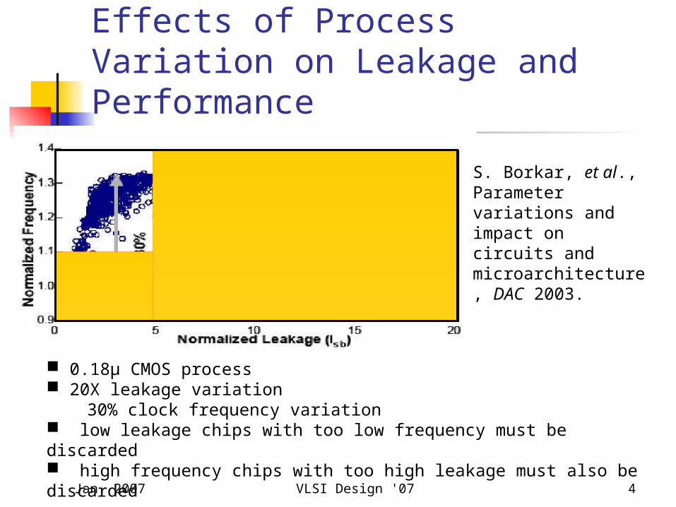
Effects of Process Variation on Leakage and Performance
too slow
too leaky
0.18µ CMOS process 20X leakage variation 30% clock frequency variation low leakage chips with too low frequency must be discarded high frequency chips with too high leakage must also be discarded
S. Borkar, et al., Parameter variations and impact on circuits and microarchitecture, DAC 2003.

Jan. 2007 VLSI Design '07 5
Leakage in C432 Due to Global Process Variation (3σ = 15%, Spice simulation)
0.000
0.050
0.100
0.150
0.200
0.250
Normalized Leakage Power
Pro
bab
ility
Global Leff+Tox+VthGlobal LeffGlobal ToxGlobal Vth
• Subthreshold is most sensitive to the variation in the effective gate length.

Jan. 2007 VLSI Design '07 6
Leakage in C432 Due to Local Process Variation (3σ = 15%)
0.000
0.200
0.400
0.600
0.800
1.000
Normalized Leakage Power
Pro
bab
ility
Local Leff+Tox+VthLocal LeffLocal ToxLocal Vth
• Subthreshold is most sensitive to the variation in the effective gate length.
Jan. 2007 VLSI Design '07 7
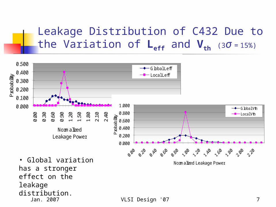
Leakage Distribution of C432 Due to the Variation of Leff and Vth (3σ = 15%)
0.000
0.100
0.200
0.300
0.400
0.500
0.00
0.30
0.60
0.90
1.20
1.50
1.80
2.10
2.40
2.70
3.00
3.30
3.60
3.90
4.20
4.50
4.80
NormalizedLeakage Power
Prob
abilit
y
Global LeffLocal Leff
• Global variation has a stronger effect on the leakage distribution.
0.000
0.200
0.400
0.600
0.800
1.000
Normalized Leakage Power
Prob
abilit
y
Global VthLocal Vth
Jan. 2007 VLSI Design '07 8
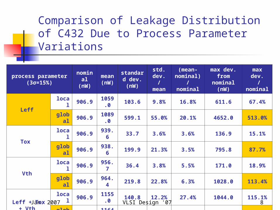
process parameter
(3σ=15%)nominal
(nW)mean(nW)
standard dev. (nW)
std. dev.
/ mean
(mean-nominal)/ nominal
max dev. from nominal
(nW)
max dev. / nominal
Leff local 906.9 1059.0 103.6 9.8% 16.8% 611.6 67.4%
global 906.9 1089.0 599.1 55.0% 20.1% 4652.0 513.0%
Tox local 906.9 939.6 33.7 3.6% 3.6% 136.9 15.1%
global 906.9 938.6 199.9 21.3% 3.5% 795.8 87.7%
Vth local 906.9 956.7 36.4 3.8% 5.5% 171.0 18.9%
global 906.9 964.4 219.8 22.8% 6.3% 1028.0 113.4%
Leff + Tox + Vth
local 906.9 1155.0 140.8 12.2% 27.4% 1044.0 115.1%
global 906.9 1164.0 719.4 61.8% 28.3% 5040.0 555.7%
Comparison of Leakage Distribution of C432 Due to Process Parameter Variations

Jan. 2007 VLSI Design '07 9
Statistical Leakage Modeling
R. Rao, et al. “Parametric Yield Estimation Considering Leakage Variability,” DAC 2004.

Jan. 2007 VLSI Design '07 10
Statistical Delay Modeling
03
02
01, 1
dop
dopi
ox
oxi
eff
effiinomi N
Nc
T
Tc
L
LcDD
thdd
dd
VV
CVD
i i
iiXthth X
XXVV
i
0
00
Let 0
30
20
1dop
dopi
ox
oxi
eff
effii N
Nc
T
Tc
L
Lcr
Deterministic Statistical – normal distribution
Mean
Standard Deviation DiiDi r inomD D
i ,
A. Davoodi and A. Srivastava, “Probabilistic Dual-Vth Optimization Under Variability,”
Proc. ISLPED, 2005.
Jan. 2007 VLSI Design '07 11
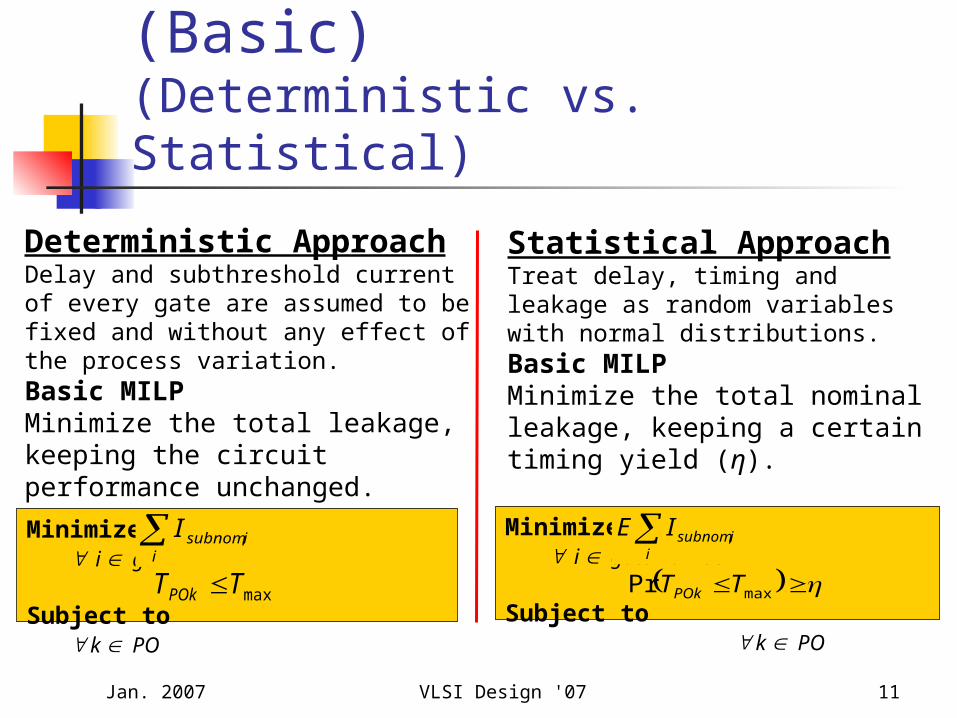
MILP Formulation (Basic)(Deterministic vs. Statistical)
Deterministic ApproachDelay and subthreshold current of every gate are assumed to be fixed and without any effect of the process variation.Basic MILP Minimize the total leakage, keeping the circuit performance unchanged.
Minimize i gate number
Subject to k PO
i
isubnomI ,
maxTTPOk
Statistical ApproachTreat delay, timing and leakage as random variables with normal distributions.Basic MILP Minimize the total nominal leakage, keeping a certain timing yield (η).
Minimize i gate number
Subject to k PO
i
isubnomIE ,
maxPr TTPOk

Jan. 2007 VLSI Design '07 12
Real Variables of MILP Delay of gate i, Di , is a Gaussian
random variable N(µDi , σDi) Maximum signal arrival time at the
output of gate i, Ti , is a Gaussian random variable N(µTi , σTi)
For gate i with input from gate j,Ti ≥ Tj + Di , µTi ≥ µTj + µDi
A linear approximation used for σTi

Jan. 2007 VLSI Design '07 13
Integer Variables of MILP For gate i, Xi = [0, 1]
Ileakage, i = ILi Xi + IHi (1 – Xi) Di = DLi Xi + DHi (1 – Xi) Where ILi , IHi , DLi , and DHi are
determined by Spice simulation of gate i

Jan. 2007 VLSI Design '07 14
Leakage Power Saving Due to Statistical Modeling with Different Timing Yields (η)
CircuitDeterministic
Opti. (η = 100%)
Statistical Optimization (η = 99%)
Statistical Optimization (η = 95%)
Circuit Name
# gates
Un-opt. Leakage Power (μW)
Optimized
Leakage Power (μW)
Run Time
(s)
Optimized Leakage Power (μW)
Extra Power Saving
Run Time
(s)
Optimized Leakage Power (μW)
Extra Power Saving
Run Time
(s)
C432 160 2.620 1.003 0.00 0.662 33.9% 0.44 0.589 41.3% 0.32
C499 182 4.293 3.396 0.02 3.396 0.0% 0.22 2.323 31.6% 1.47
C880 328 4.406 0.526 0.02 0.367 30.2% 0.18 0.340 35.4% 0.18
C1355 214 4.388 3.153 0.00 3.044 3.5% 0.17 2.158 31.6% 0.48
C1908 319 6.023 1.179 0.03 1.392 21.7% 11.21 1.169 34.3% 17.45
C2670 362 5.925 0.565 0.03 0.298 47.2% 0.35 0.283 49.8% 0.43
C3540 1097 15.622 0.957 0.13 0.475 50.4% 0.24 0.435 54.5% 1.17
C5315 1165 19.332 2.716 1.88 1.194 56.0% 67.63 0.956 64.8% 19.7
C7552 1045 22.043 0.938 0.44 0.751 20.0% 0.88 0.677 27.9% 0.58
Average of ISCAS’85 benchmarks 0.24 29.2% 9.04 41.3% 4.64
ARM7 15.5k 686.56 495.12 15.69 425.44 14.07% 36.79 425.44 14.07% 36.44

Jan. 2007 VLSI Design '07 15
Power-Delay Curves of Statistical and Deterministic Approaches for C432
1 1.05 1.1 1.15 1.2 1.25 1.3 1.35 1.4 1.45 1.50
0.1
0.2
0.3
0.4
0.5
0.6
0.7
0.8
0.9
1
Normalized Timing
Nor
mal
ized
Lea
kage
Pow
er
Deterministic LP
Statistical LP ( 99% Timing Yield)
Statistical LP ( 95% Timing Yield)
When performance is kept unchanged:
Leakage power reduced by deterministic approach normalized to 1 unit.
0.65 unit and 0.59 unit leakage power achieved by statistical approach with 99% and 95% timing yields, respectively.
Lower the timing yield, higher is power saving.
With a further relaxed Tmax , all three curves will give more reduction in leakage power.

Jan. 2007 VLSI Design '07 16
Leakage Power Distribution with Different Timing Yields (η)
CircuitDeterministic Optimization
(η =100%)Statistical Optimization
(η = 99%)Statistical Optimization
(η = 95%)
Name#
gates
Nominal Leakage
(uW)
Mean Leakage
(uW)
Standard Deviation
(uw)
Nominal Leakage
(uW)
Mean Leakage
(uW)
Standard Deviation
(uW)
Nominal Leakage
(uW)
Mean Leakage
(uW)
Standard Deviation
(uW)
C432 160 0.907 1.059 0.104 0.603 0.709 0.074 0.522 0.614 0.069
C499 182 3.592 4.283 0.255 3.592 4.283 0.255 2.464 2.905 0.197
C880 328 0.551 0.645 0.086 0.430 0.509 0.080 0.415 0.491 0.079
C1355 214 3.198 3.744 0.200 3.090 3.606 0.202 2.199 2.610 0.175
C1908 319 1.803 2.123 0.170 1.356 1.601 0.116 1.140 1.341 0.127
C2670 362 0.635 0.750 0.078 0.405 0.473 0.046 0.395 0.461 0.043
C3540 1097 1.055 1.243 0.119 0.527 0.611 0.032 0.493 0.575 0.031
C5315 1165 2.688 3.128 0.165 1.229 1.420 0.088 1.034 1.188 0.067
C7552 1045 0.924 1.073 0.069 0.774 0.903 0.049 0.701 0.823 0.045
Average of ISCAS’85 benchmarks 0.138 0.105 0.085

Jan. 2007 VLSI Design '07 17
Leakage Power Distribution of Optimized Dual-Vth C7552
0.000
0.050
0.100
0.150
0.200
0.250
0
1.00
E-07
2.00
E-07
3.00
E-07
4.00
E-07
5.00
E-07
6.00
E-07
7.00
E-07
8.00
E-07
9.00
E-07
1.00
E-06
1.10
E-06
1.20
E-06
1.30
E-06
1.40
E-06
Leakage Power (micro W)
Pro
babi
lity
C7552_d
C7552_p99
C7552_p95
Jan. 2007 VLSI Design '07 18
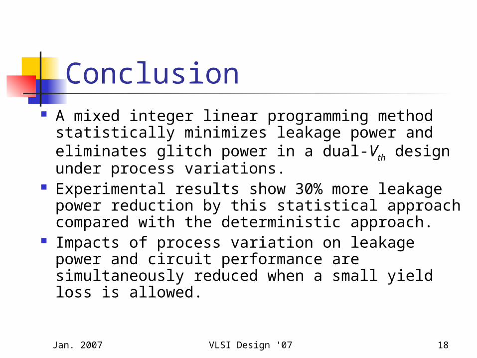
Conclusion A mixed integer linear programming method
statistically minimizes leakage power and eliminates glitch power in a dual-Vth design under process variations.
Experimental results show 30% more leakage power reduction by this statistical approach compared with the deterministic approach.
Impacts of process variation on leakage power and circuit performance are simultaneously reduced when a small yield loss is allowed.