challenges of deep submicron design -...
TRANSCRIPT

Nanometer flow: 1
Jacques-Olivier Piednoir
Cadence, VP R&D Europe
Challenges of Deep Submicron Design
Marc Heyberger
Cadence, Product Engineer
Nanometer flow: 2
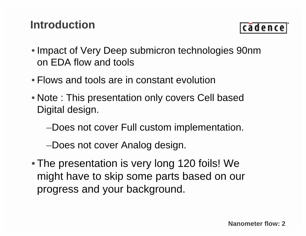
Introduction
• Impact of Very Deep submicron technologies 90nm on EDA flow and tools
• Flows and tools are in constant evolution
• Note : This presentation only covers Cell based Digital design.
–Does not cover Full custom implementation.
–Does not cover Analog design.
• The presentation is very long 120 foils! We might have to skip some parts based on our progress and your background.
Nanometer flow: 3
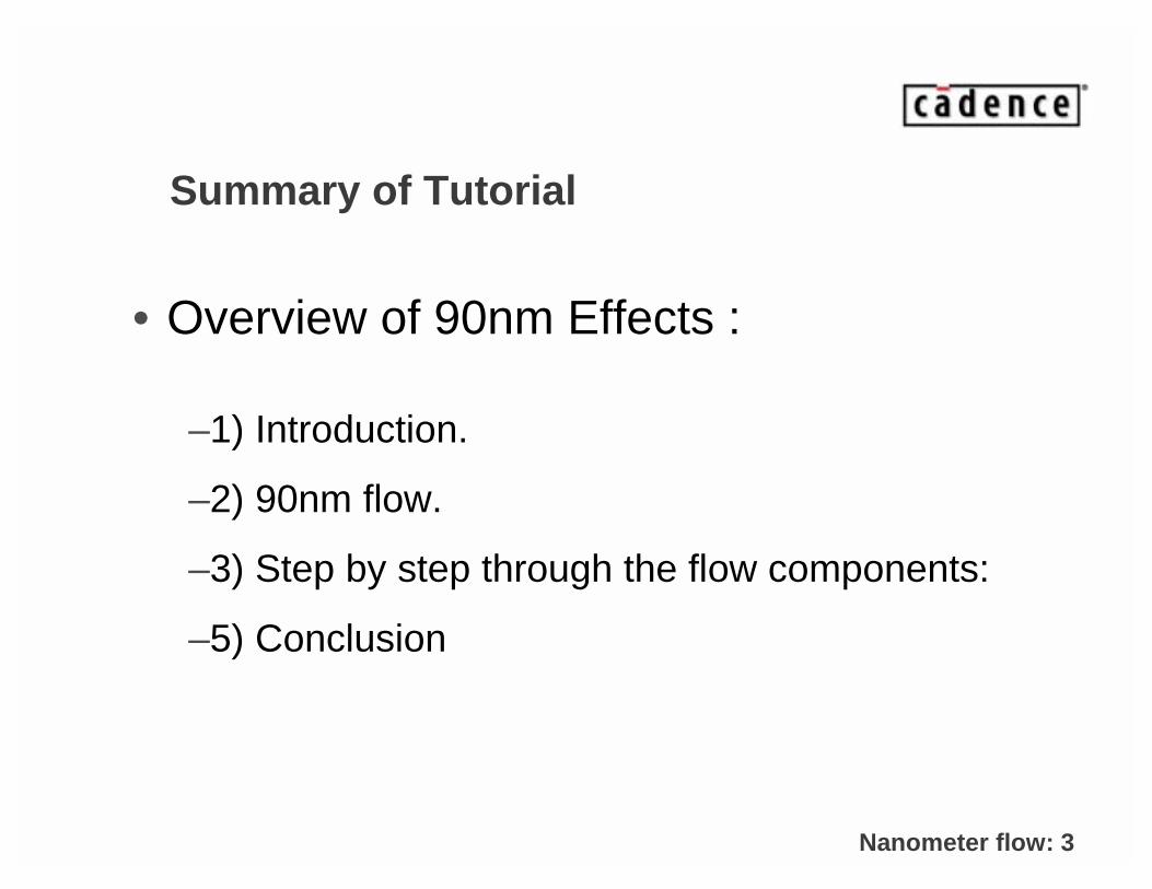
Summary of Tutorial
• Overview of 90nm Effects :
–1) Introduction.
–2) 90nm flow.
–3) Step by step through the flow components:
–5) Conclusion
Nanometer flow: 4
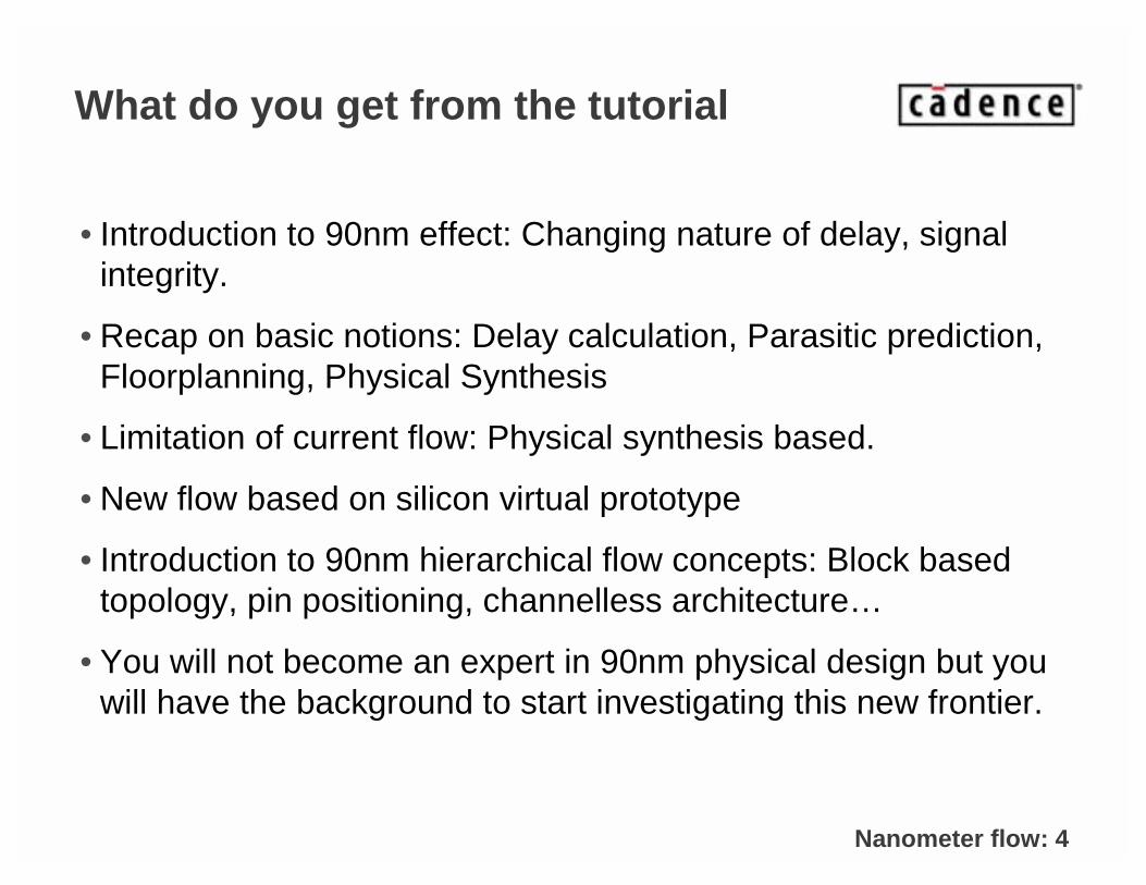
What do you get from the tutorial
• Introduction to 90nm effect: Changing nature of delay, signal integrity.
• Recap on basic notions: Delay calculation, Parasitic prediction,Floorplanning, Physical Synthesis
• Limitation of current flow: Physical synthesis based.
• New flow based on silicon virtual prototype
• Introduction to 90nm hierarchical flow concepts: Block based topology, pin positioning, channelless architecture…
• You will not become an expert in 90nm physical design but you will have the background to start investigating this new frontier.
Nanometer flow: 5
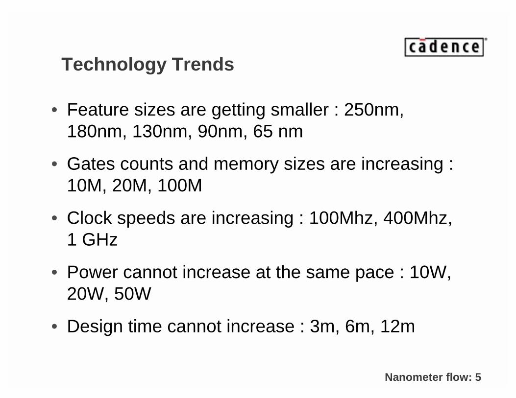
Technology Trends
• Feature sizes are getting smaller : 250nm, 180nm, 130nm, 90nm, 65 nm
• Gates counts and memory sizes are increasing : 10M, 20M, 100M
• Clock speeds are increasing : 100Mhz, 400Mhz, 1 GHz
• Power cannot increase at the same pace : 10W, 20W, 50W
• Design time cannot increase : 3m, 6m, 12m
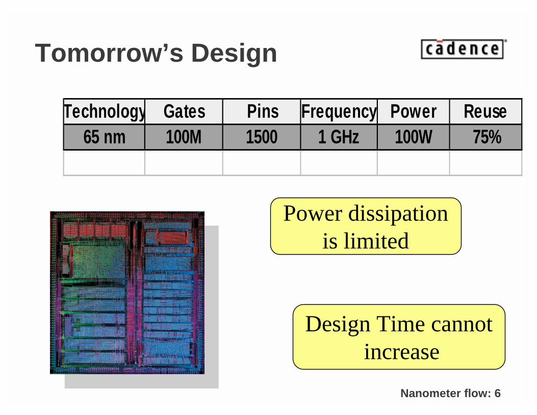
Nanometer flow: 6
Tomorrow’s Design
Technology Gates Pins Frequency Power Reuse65 nm 100M 1500 1 GHz 100W 75%
Power dissipationis limited
Design Time cannotincrease

CADENCE CONFIDENTIAL
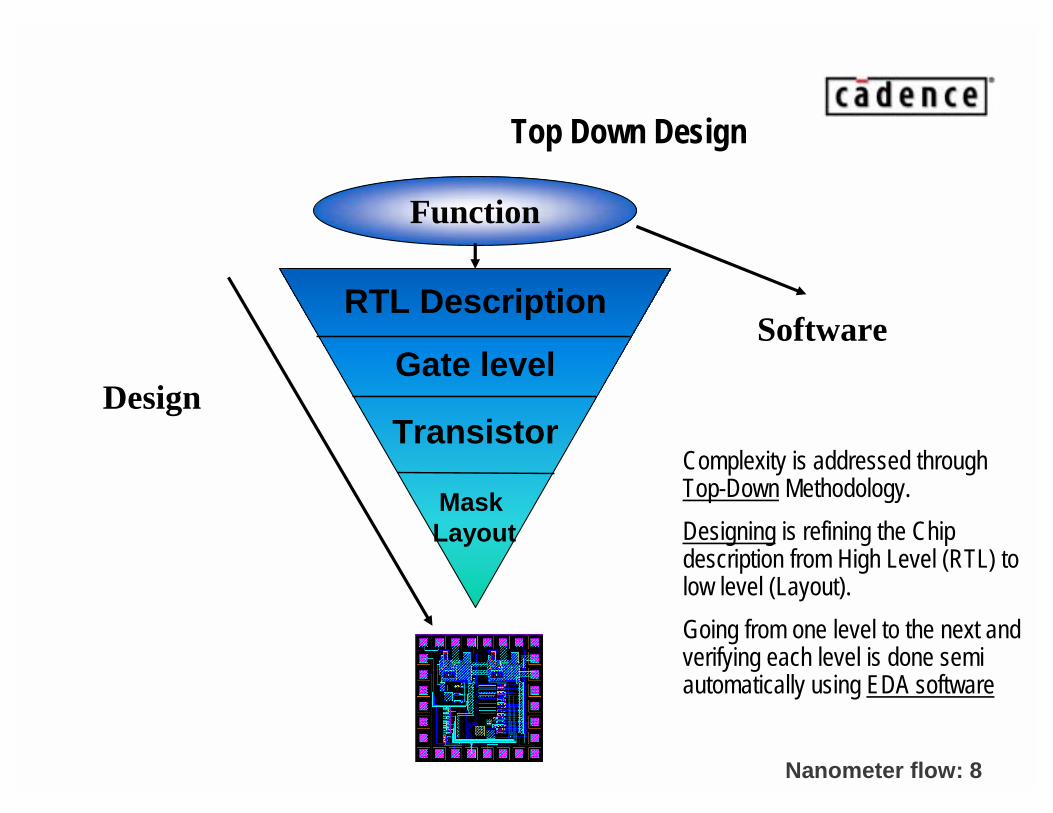
Chapter 1) Short Overview of Top Down
Design Methodology.
Recap for beginners in the field.Can be skipped with students with design experience.
Nanometer flow: 8
Design
Software
Function
RTL Description
Gate level
Transistor
MaskLayout
Top Down Design
Complexity is addressed through Top-Down Methodology.
Designing is refining the Chip description from High Level (RTL) to low level (Layout).
Going from one level to the next and verifying each level is done semi automatically using EDA software
Nanometer flow: 9
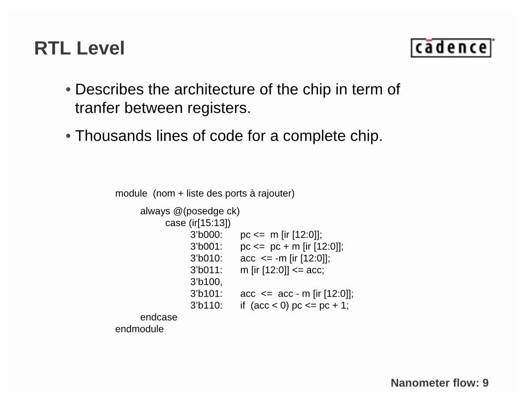
RTL Level
• Describes the architecture of the chip in term of tranfer between registers.
• Thousands lines of code for a complete chip.
module (nom + liste des ports à rajouter)
always @(posedge ck)case (ir[15:13])
3’b000: pc <= m [ir [12:0]];3’b001: pc <= pc + m [ir [12:0]];3’b010: acc <= -m [ir [12:0]];3’b011: m [ir [12:0]] <= acc;3’b100,3’b101: acc <= acc - m [ir [12:0]]; 3’b110: if (acc < 0) pc <= pc + 1;
endcaseendmodule
Nanometer flow: 10
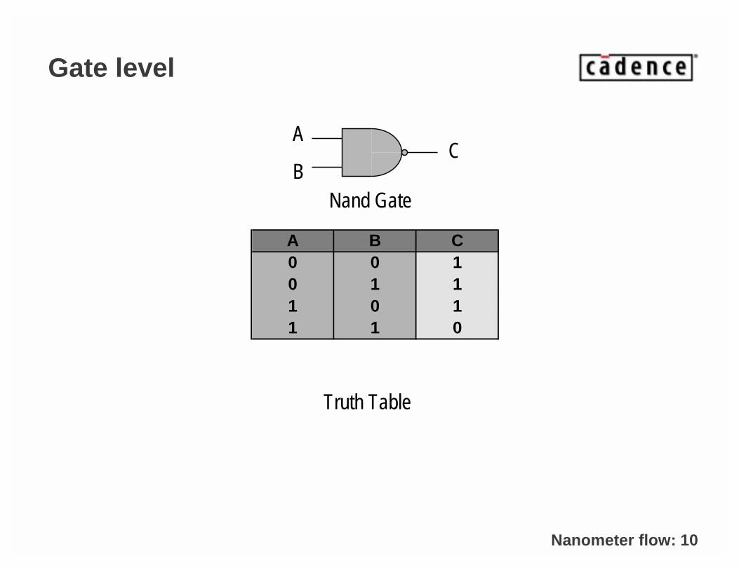
Gate level
A B C0 0 10 1 11 0 11 1 0
A
BC
Nand Gate
Truth Table
Nanometer flow: 11
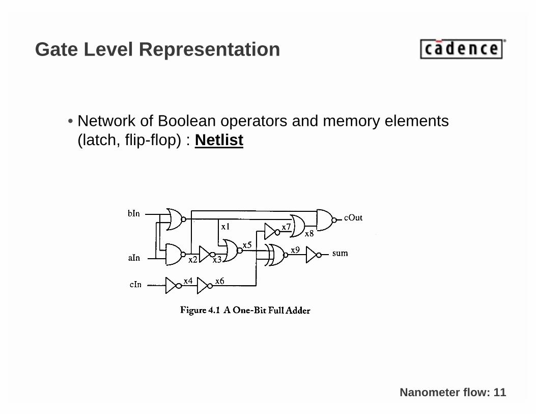
Gate Level Representation
• Network of Boolean operators and memory elements (latch, flip-flop) : Netlist
Nanometer flow: 12
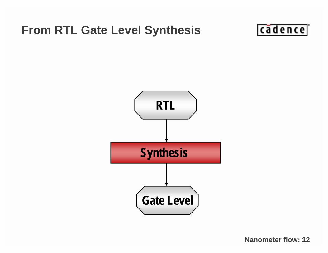
From RTL Gate Level Synthesis
Synthesis
RTL
Gate Level
Nanometer flow: 13
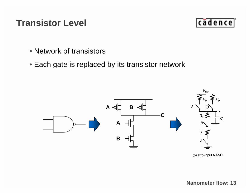
Transistor Level
• Network of transistors
• Each gate is replaced by its transistor network
A
A
B
BC
Nanometer flow: 14
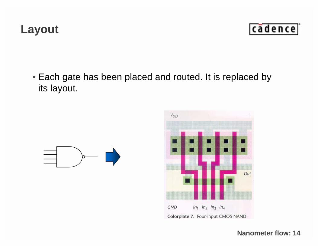
Layout
• Each gate has been placed and routed. It is replaced by its layout.
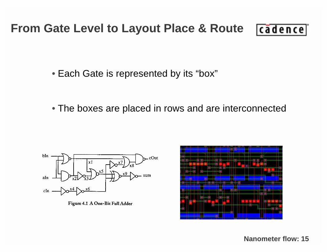
Nanometer flow: 15
From Gate Level to Layout Place & Route
• Each Gate is represented by its “box”
• The boxes are placed in rows and are interconnected
Nanometer flow: 16
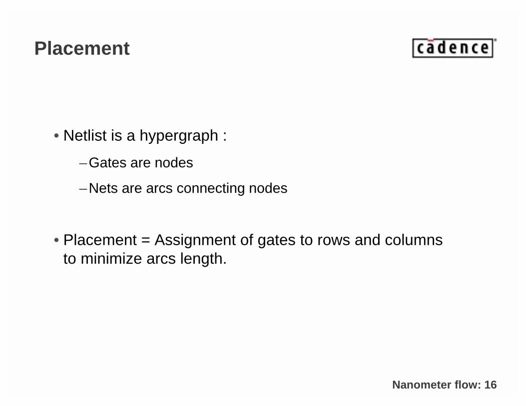
Placement
• Netlist is a hypergraph :
–Gates are nodes
–Nets are arcs connecting nodes
• Placement = Assignment of gates to rows and columns to minimize arcs length.
Nanometer flow: 17
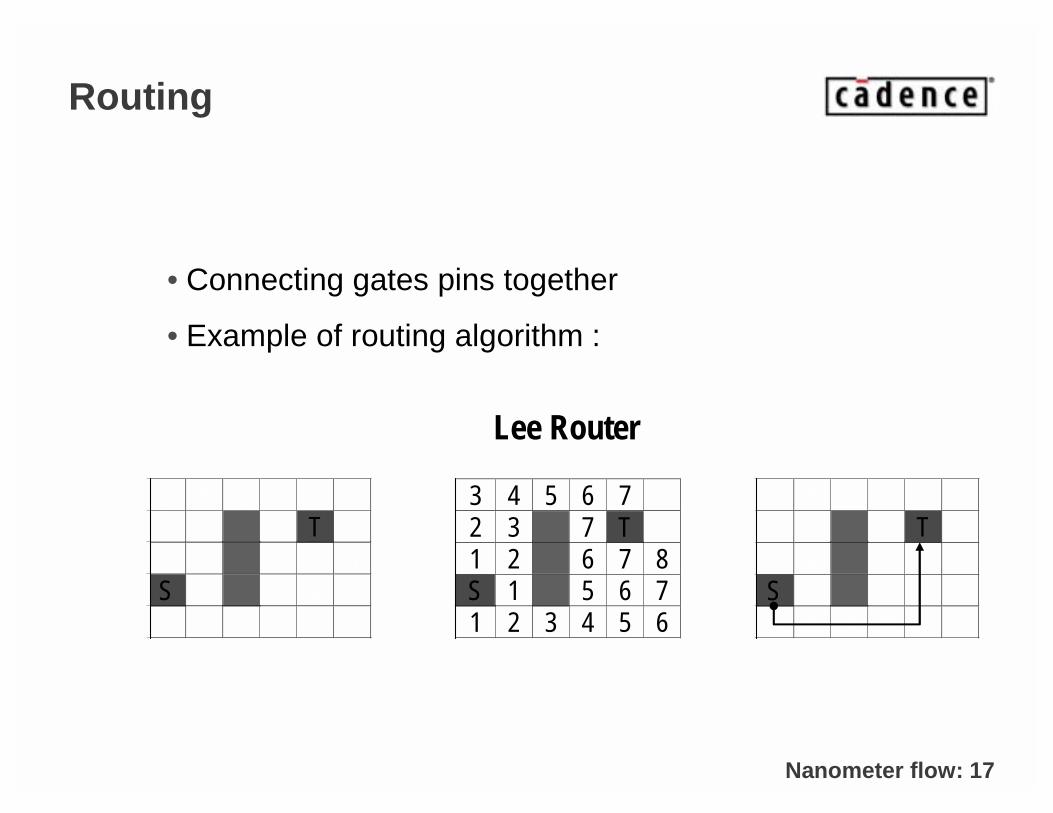
Routing
• Connecting gates pins together
• Example of routing algorithm :
Lee Router
3 4 5 6 72 3 7 T1 2 6 7 8S 1 5 6 71 2 3 4 5 6
3 4 5 6 72 3 7 T1 2 6 7 8S 1 5 6 71 2 3 4 5 6
3 4 5 6 72 3 7 T1 2 6 7 8S 1 5 6 71 2 3 4 5 6
Nanometer flow: 18
Verification
• At each level (RTL, Gates, Layout) the design must be verified :
–Does it perform the right function ?
–Does it work at the right speed ?
• Two types of verification
–Dynamic : Create a software prototype of the design. Exercise it with software stimuli.
–Static :
– Functional level : Prove design correctness through equivalence or property checking
– Timing level : Compute design speed through graph traversal techniques
Nanometer flow: 19
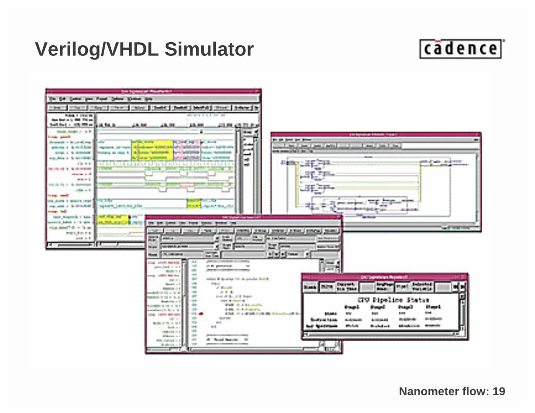
Verilog/VHDL Simulator
Nanometer flow: 20
Simulation Challenges
• Simulation run can be very longs : days of CPU.
• Whole Chip can only be simulated at the RTL level.
• Sub components are simulated at gate or transistor level.
• Stimuli generation and results analysis is a complex problem.
–Stimuli can be data : 0, 1, (C or C++Code).
–Analysis can be visual (waveforms) or automatic (observers).

Nanometer flow: 21
Static timing Verification
5 ns8 ns
� Compute the speed at which a signal propagates through the design.
� Used to compute the clock frequency.
� Implemented using graph traversal algorithms (shortest, longest path).
Nanometer flow: 22
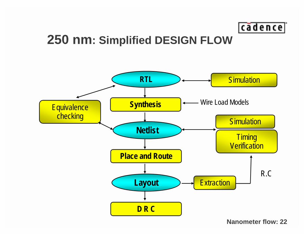
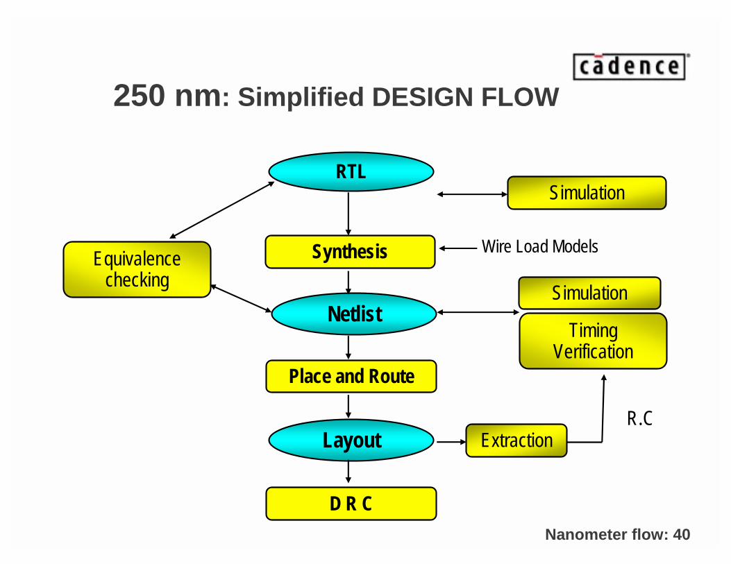
250 nm: Simplified DESIGN FLOW
RTL
Layout
Netlist
Synthesis
Place and Route
D R C
Equivalence checking
Simulation
Simulation
ExtractionR.C
Timing Verification
Wire Load Models
CADENCE CONFIDENTIAL
Chapter 2) 90 nanometer design challenges.
Nanometer flow: 24
90 nanometer design flow
• Wire-Wire-Wire everywhere
• Changing nature of Delay
– Cross coupling
– IR Drop
• History of flow from 250nm to 90nm.
• 90nm flow Continuous convergence.
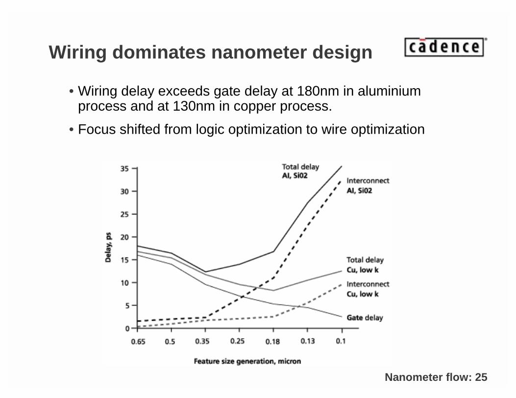
Nanometer flow: 25
Wiring dominates nanometer design
• Wiring delay exceeds gate delay at 180nm in aluminiumprocess and at 130nm in copper process.
• Focus shifted from logic optimization to wire optimization
Nanometer flow: 26
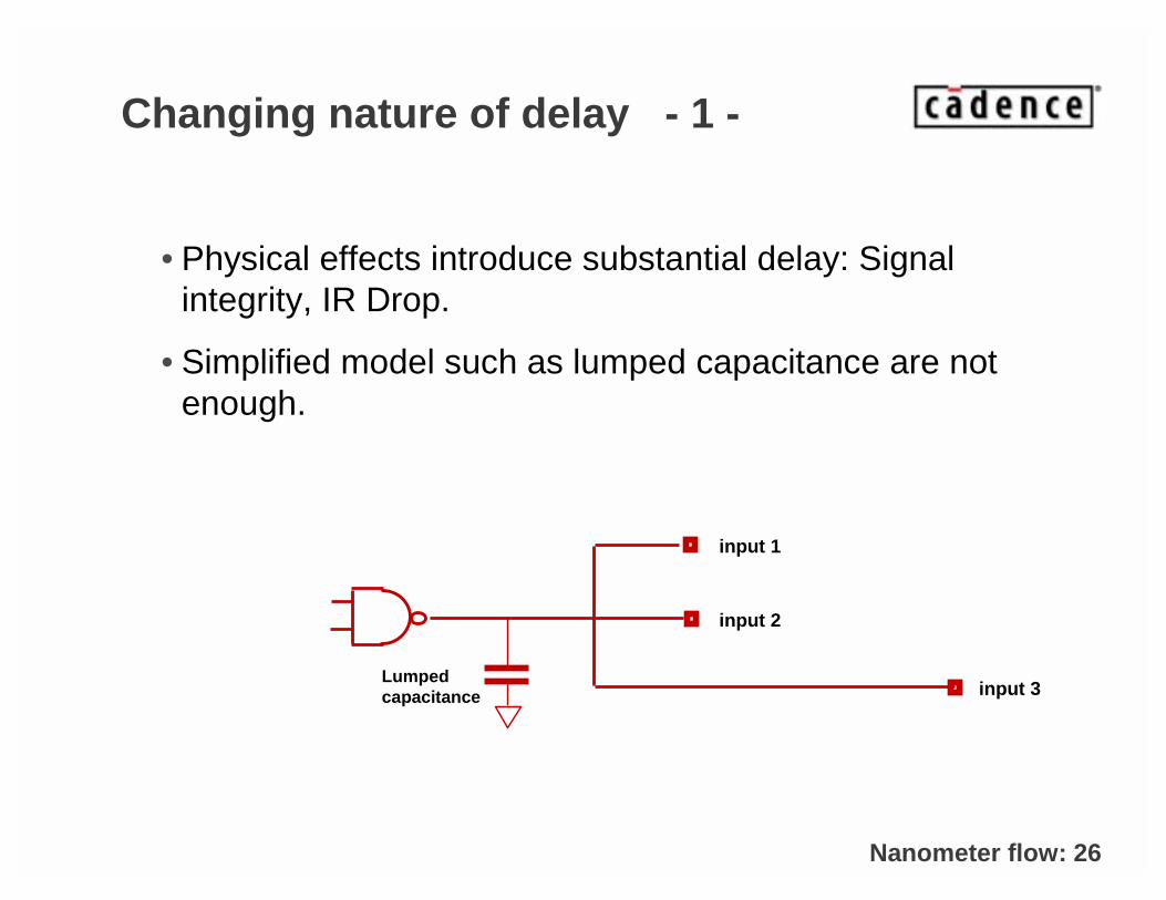
Changing nature of delay - 1 -
• Physical effects introduce substantial delay: Signal integrity, IR Drop.
• Simplified model such as lumped capacitance are notenough.
Lumpedcapacitance
input 1
input 2
input 3
Nanometer flow: 27
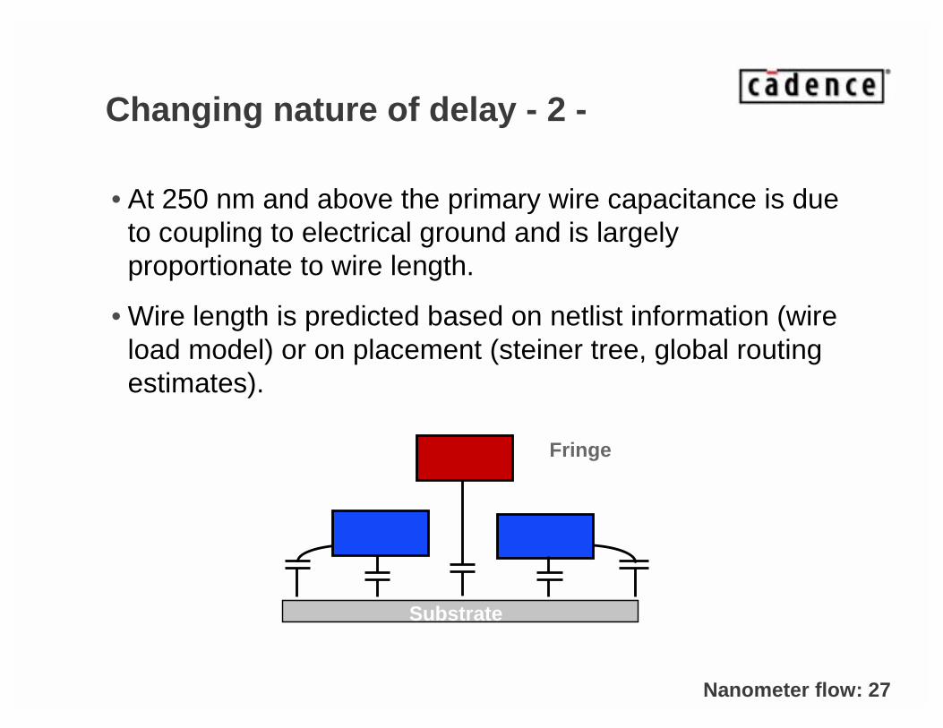
Changing nature of delay - 2 -
• At 250 nm and above the primary wire capacitance is due to coupling to electrical ground and is largelyproportionate to wire length.
• Wire length is predicted based on netlist information (wireload model) or on placement (steiner tree, global routingestimates).
Substrate
Fringe
Nanometer flow: 28
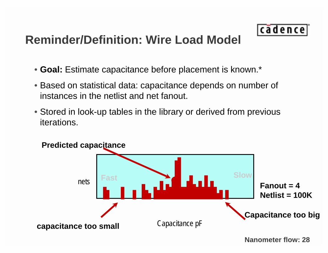
Reminder/Definition: Wire Load Model
• Goal: Estimate capacitance before placement is known.*
• Based on statistical data: capacitance depends on number ofinstances in the netlist and net fanout.
• Stored in look-up tables in the library or derived from previousiterations.
Predicted capacitance
Fanout = 4Netlist = 100K
SlowFast
capacitance too smallCapacitance too big
Capacitance pF
nets
Nanometer flow: 29
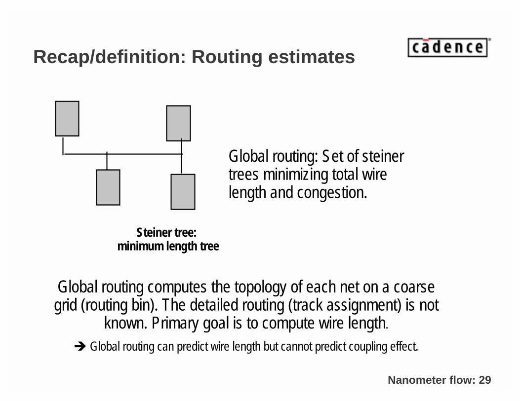
Recap/definition: Routing estimates
Steiner tree: minimum length tree
Global routing: Set of steinertrees minimizing total wire length and congestion.
Global routing computes the topology of each net on a coarse grid (routing bin). The detailed routing (track assignment) is not
known. Primary goal is to compute wire length.
� Global routing can predict wire length but cannot predict coupling effect.
Nanometer flow: 30
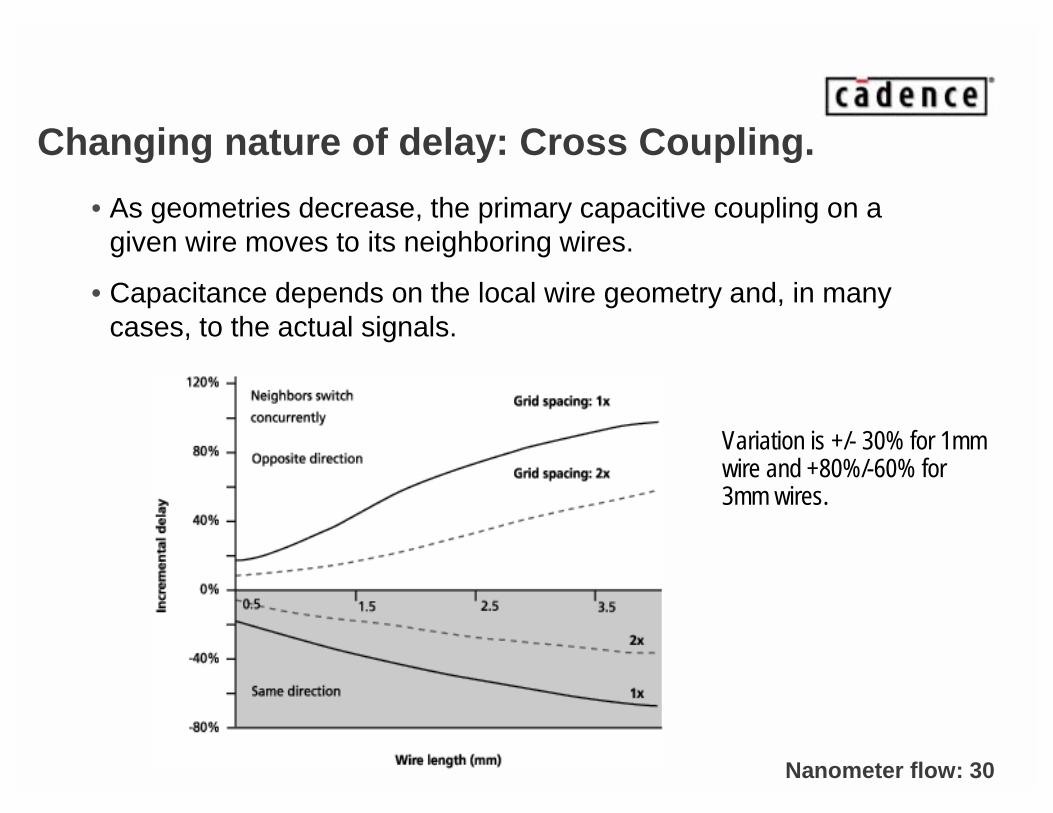
Changing nature of delay: Cross Coupling.
• As geometries decrease, the primary capacitive coupling on a given wire moves to its neighboring wires.
• Capacitance depends on the local wire geometry and, in many cases, to the actual signals.
Variation is +/- 30% for 1mm wire and +80%/-60% for 3mm wires.
Nanometer flow: 31
Cross coupling conclusion
• Placement based estimates steiner trees, global routing are not accurate enough. Detailed routing is required to predict performances.
• Issues:
– How can we get early access to detail routing ?
– How can we iterate fast enough when detailed routing is required ?
Nanometer flow: 32
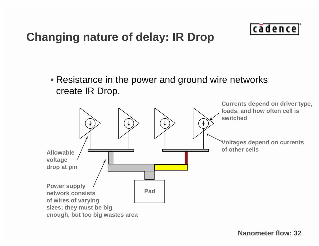
Changing nature of delay: IR Drop
• Resistance in the power and ground wire networks create IR Drop.
Voltages depend on currentsof other cells
PadPower supplynetwork consistsof wires of varyingsizes; they must be bigenough, but too big wastes area
Currents depend on driver type,loads, and how often cell isswitched
Allowablevoltagedrop at pin
Nanometer flow: 33
Changing nature of delay: IR Drop and delay
• An IR Drop from 1.7V to 1.6V is capable of producing delay variation of 50% or more.
• One study of designs at 180 nm showed that 20% of designs failed on first silicon due to excessive IR Drop alone.
• Conclusion: 90 nm flow should include a tool to compute IR Drop and a delay calculator taking into account the IR Drop.
Nanometer flow: 34
Recap: delay calculation
• Timing verification is split into two components:
– Delay calculator: computes delay between gate output and gate inputs based on extracted RCs.
– Static Timing Analysis engine: propagate the delay in the cells and in the interconnect to check for timing violations.
• 90 nm DC such as Signal Storm takes into account:
– IR Drop
– Cross talk impact on delay.
• STA tools such as Primetime, Buildgates read in an SDF file the delay computed by the Delay calculator.
Nanometer flow: 35
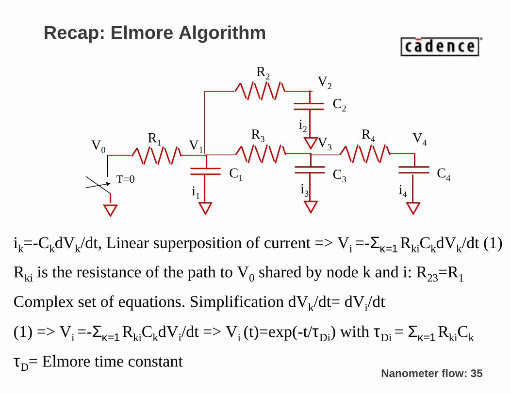
Recap: Elmore Algorithm
V0 V1V3
V2
V4
T=0 C1
R3 R4
R2
R1
C3 C4
C2
i1i3 i4
i2
ik=-CkdVk/dt, Linear superposition of current => Vi =-Σκ=1 RkiCkdVk/dt (1)
Rki is the resistance of the path to V0 shared by node k and i: R23=R1
Complex set of equations. Simplification dVk/dt= dVi/dt
(1) => Vi =-Σκ=1 RkiCkdVi/dt => Vi (t)=exp(-t/τDi) with τDi = Σκ=1 RkiCk
τD= Elmore time constant
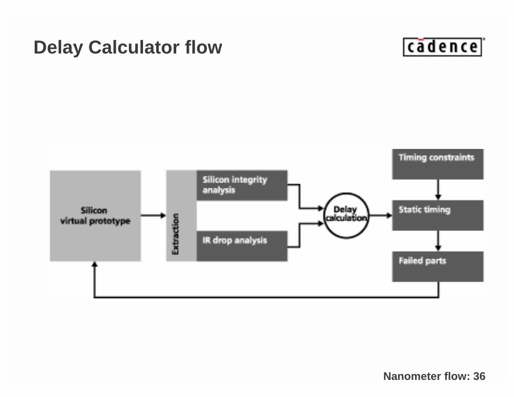
Nanometer flow: 36
Delay Calculator flow
CADENCE CONFIDENTIAL
Chapter 3) 90 nanometer design flow.
Nanometer flow: 38
What have we seen so far ?
• Delay is dominated by wires.
• Delay is dependent on SI issues (cross coupling) and IR Drop.
• �Next foils will investigate the impact of the above on the physical design flow and the physical implementation tools
Nanometer flow: 39
Nanometer design flow
• Dominance of wire delays has significantly modified the flow in the last 10 years.
• 250 nm and above:
– Gates dominate delay. Wire delay can be estimated using wire load model. Synthesis and place / route are two different steps.
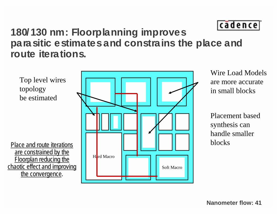
• 180-130 nm:
– Wire delay starts dominating overall delay. Better accuracy is needed in wire delay estimation:
– Placement and Synthesis merge (Physical Compiler, PKS) at the block level
– Floorplanner to estimate top level wires.
• 90 nm and below.
– Wire delay dominates the design. Wire delay depends on cross coupling �Performance is unknown before routing.
– Introduction of tools and flow that generate wires as soon as possible (“time to wire”).
Nanometer flow: 40
250 nm: Simplified DESIGN FLOW
RTL
Layout
Netlist
Synthesis
Place and Route
D R C
Equivalence checking
Simulation
Simulation
ExtractionR.C
Timing Verification
Wire Load Models
Nanometer flow: 41
180/130 nm: Floorplanning improves parasitic estimates and constrains the place and route iterations.
Wire Load Models are more accurate in small blocks
Top level wires topologybe estimated
Hard Macro
Soft MacroSoft Macro
Place and route iterations are constrained by the Floorplan reducing the
chaotic effect and improving the convergence.
Placement based synthesis can handle smaller blocks

Nanometer flow: 42
180/130 nm Placement based synthesis
Parsing, Structuring Mapping
accept /reject
Route & Timeusing fast router
Initial Placement
Optimization Transformsrestructure, clone, remap, buffer, etc
Incremental Placement
106
RTL Source Physical Constraints
SynthesisLibrary
PhysicalLibrary (LEF)
Physical ConstraintsTiming Constraints
Place and Route Place and Route Detail Placement
Detailed routing
Timing Constraints
Nanometer flow: 43
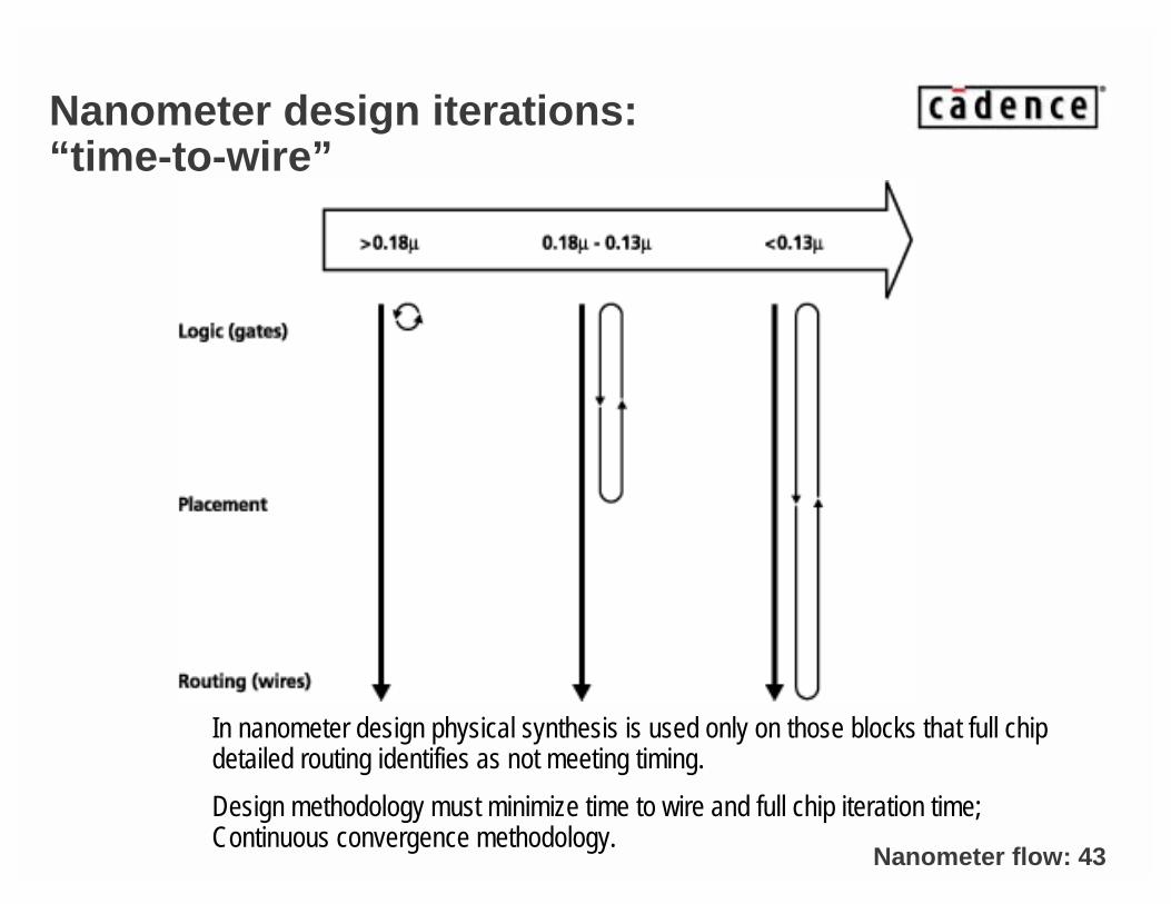
Nanometer design iterations: “time-to-wire”
In nanometer design physical synthesis is used only on those blocks that full chip detailed routing identifies as not meeting timing.
Design methodology must minimize time to wire and full chip iteration time; Continuous convergence methodology.
Nanometer flow: 44
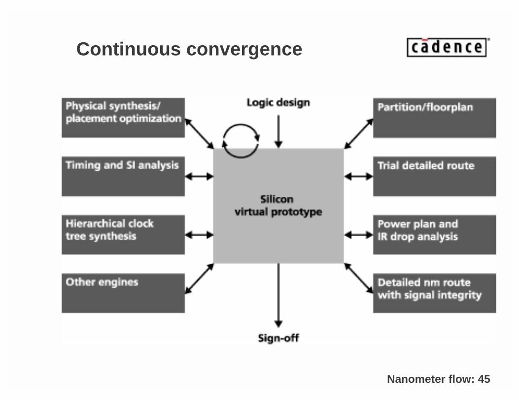
Continuous convergence
• Continuous convergence begins with an initial full chip design representation with wires called silicon virtual prototype (SVP).
• SVP treats all aspects of the design: logic, timing, SI, IR Drop, Electromigration, I/O and manufacturability.
• SVP should have a one day turn around to allow design teams to identify and prioritize performance and manufacturing issues.
• SVP is followed by a final chip implementation when all design parameters and architectures have been finalized and validated.
Nanometer flow: 45
Continuous convergence
CADENCE CONFIDENTIAL
Chapter 4) 90 nanometer hierarchical
design flow.
Introduction of hierarchy concept in the design flow.
Nanometer flow: 47
What have we learned sofar
• 90nm effects require a new flow focus on wires which provide an early access to detailed routing (Silicon Virtual Prototype).
• � Next chapters will introduce the concepts used in hierarchical design and visit in details each component of the hierarchical 90nm flow
• Some chapters focusing on hierarchical physical design can be skipped if time is too short.
Nanometer flow: 48
Hierarchical 90 nm flow.
• Hierarchical approach:
– Decompose Chip design problem into:– Partitioning design into sub-designs.
– Define top level topology: Block placement, pin positioning, power planning.
– Budget top level constraints into block constraints
– Implement blocks concurrently
– Perform Chip Assembly: top level routing, top level clock planning, power routing.
• Hierarchical design methodology is required for:
– Very large design which cannot be handle flat. Flat is the default mode.
– Concurrent engineering.
• Timing closure in a hierarchical flow is more complex than in a flat flow due to the budgeting and the full chip verification problems.
Nanometer flow: 49
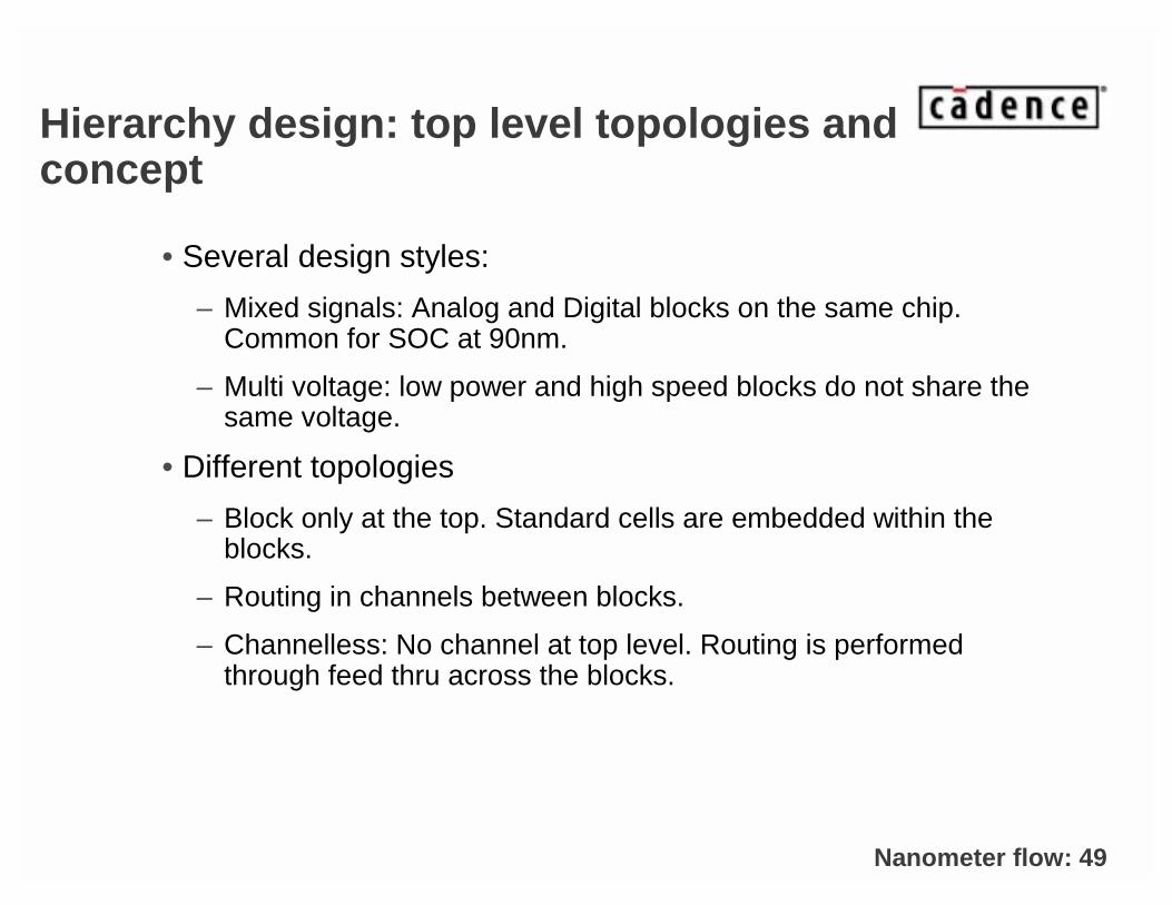
Hierarchy design: top level topologies and concept
• Several design styles:
– Mixed signals: Analog and Digital blocks on the same chip. Common for SOC at 90nm.
– Multi voltage: low power and high speed blocks do not share the same voltage.
• Different topologies
– Block only at the top. Standard cells are embedded within the blocks.
– Routing in channels between blocks.
– Channelless: No channel at top level. Routing is performed through feed thru across the blocks.
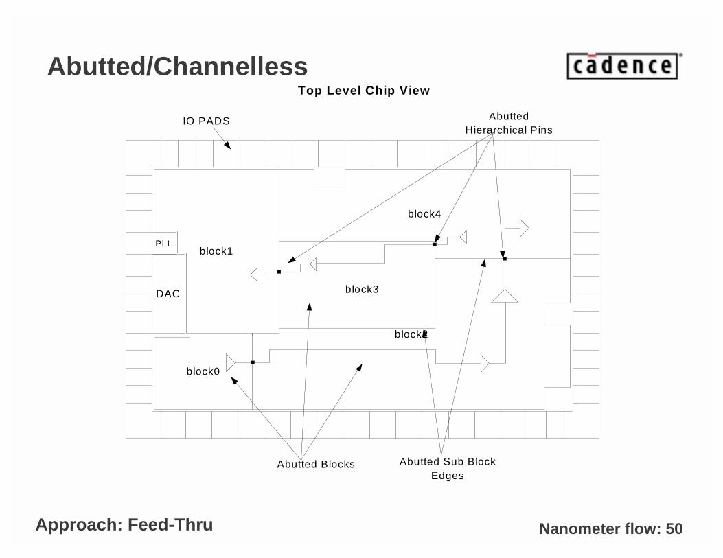
Nanometer flow: 50
Abutted/Channelless
block3
block1
block2
block4
PLL
DAC
block0
Top Level Chip View
IO PADS
Abutted Blocks Abutted Sub BlockEdges
AbuttedHierarchical Pins
Approach: Feed-Thru
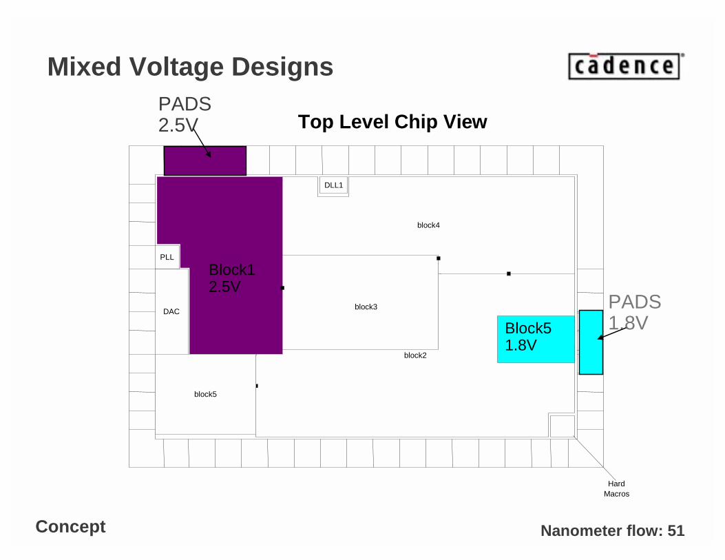
Nanometer flow: 51
Mixed Voltage Designs
block3
Block1 2.5V
block2
block4
PLL
DAC
Top Level Chip ViewPADS2.5V
block5
DLL1
Block51.8V
HardMacros
Concept
PADS1.8V
Nanometer flow: 52
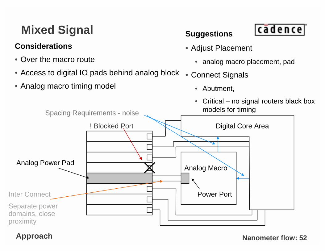
Mixed SignalConsiderations
• Over the macro route
• Access to digital IO pads behind analog block
• Analog macro timing model
Analog Power PadAnalog Macro
Power Port
Digital Core Area! Blocked Port
Spacing Requirements - noise
Inter Connect
Separate power domains, close proximity
Approach
Suggestions
• Adjust Placement
• analog macro placement, pad
• Connect Signals
• Abutment,
• Critical – no signal routers black box models for timing
Nanometer flow: 53
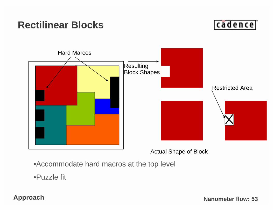
Rectilinear Blocks
Resulting Block Shapes
Hard Marcos
•Accommodate hard macros at the top level
•Puzzle fit
Approach
Actual Shape of Block
Restricted Area
Nanometer flow: 54
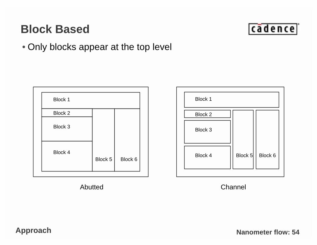
Block Based• Only blocks appear at the top level
Block 1
Block 2
Block 3
Block 4Block 5 Block 6
Block 1
Block 2
Block 3
Block 4 Block 5 Block 6
Abutted Channel
Approach
Nanometer flow: 55
Through the flow step by step
• Partitioning
• Pin positioning.
• Power distribution
• Hierarchical Clock Distribution
• Parasitic extraction
• Timing analysis
• Signal integrity
• Power analysis
CADENCE CONFIDENTIAL
Partitioning
Through the flow Step by Step
Nanometer flow: 57
Partitioning
• Maps logical hierarchy into physical hierarchy.
• Physical hierarchy must be included into logical hierarchy
– Not every VHDL architecture or Verilog module is a physical block
– But each physical block must correspond to an architecture.
• Partitioning takes into account:
– Power planning: multiple power domain (low power, analog block).
– IP reuse.
– Concurrent engineering over several teams.
– Top level topology: channel based, rectilinear blocks, block based…
– Block implementation size (requires fast synthesis for prediction of block size at RTL level).
Nanometer flow: 58
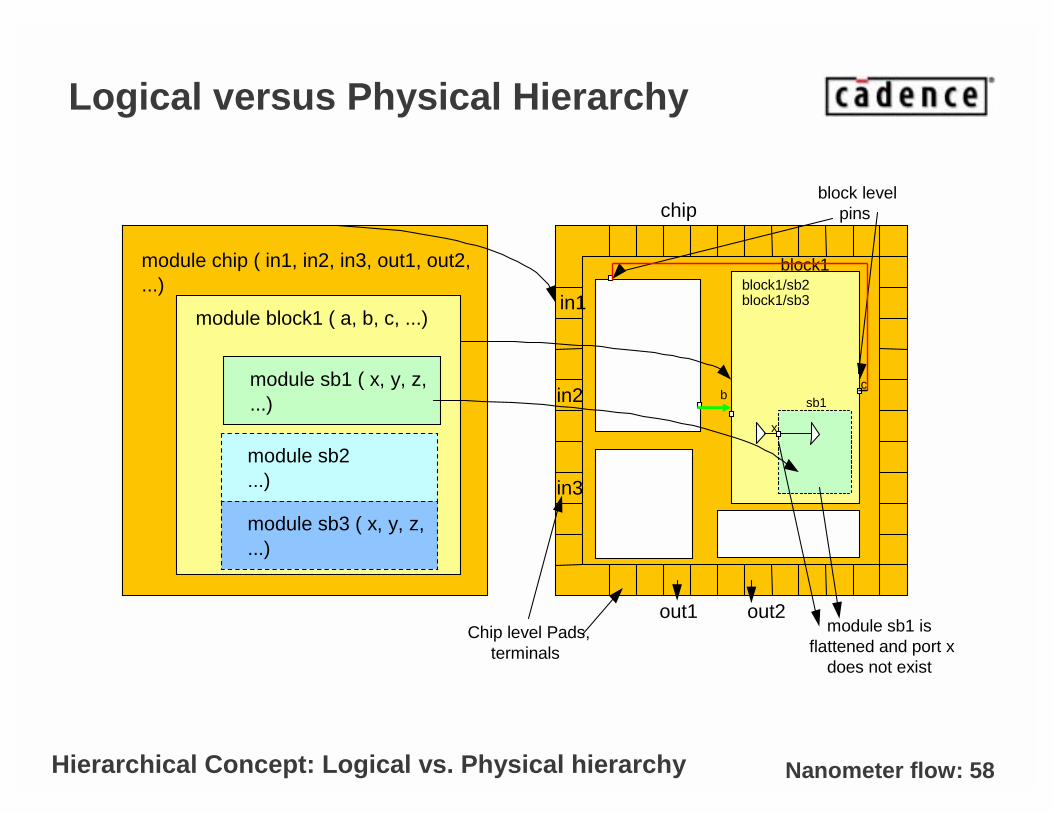
Logical versus Physical Hierarchy
module chip ( in1, in2, in3, out1, out2,...)
module block1 ( a, b, c, ...)
module sb1 ( x, y, z,...)
block1/sb2block1/sb3in1
in2
in3
out1 out2
bc
x
module sb1 isflattened and port x
does not exist
Chip level Pads,terminals
block levelpins
block1
sb1
chip
module sb2...)
module sb3 ( x, y, z,...)
Hierarchical Concept: Logical vs. Physical hierarchy
CADENCE CONFIDENTIAL
Pin Optimization
Through the flow step by step
Nanometer flow: 60
Overview
• Motivation– Create top-level interconnect strategy to ensure routability and timing
closure.
• General Pin Optimization Concepts– Constraints
– Supply vs. Signal
– Accessibility
– Rule Checking
– Uniqueness
• Approaches– Top-down or Bottom-up
– Pin Guides
– Feedthrus
Overview
Nanometer flow: 61
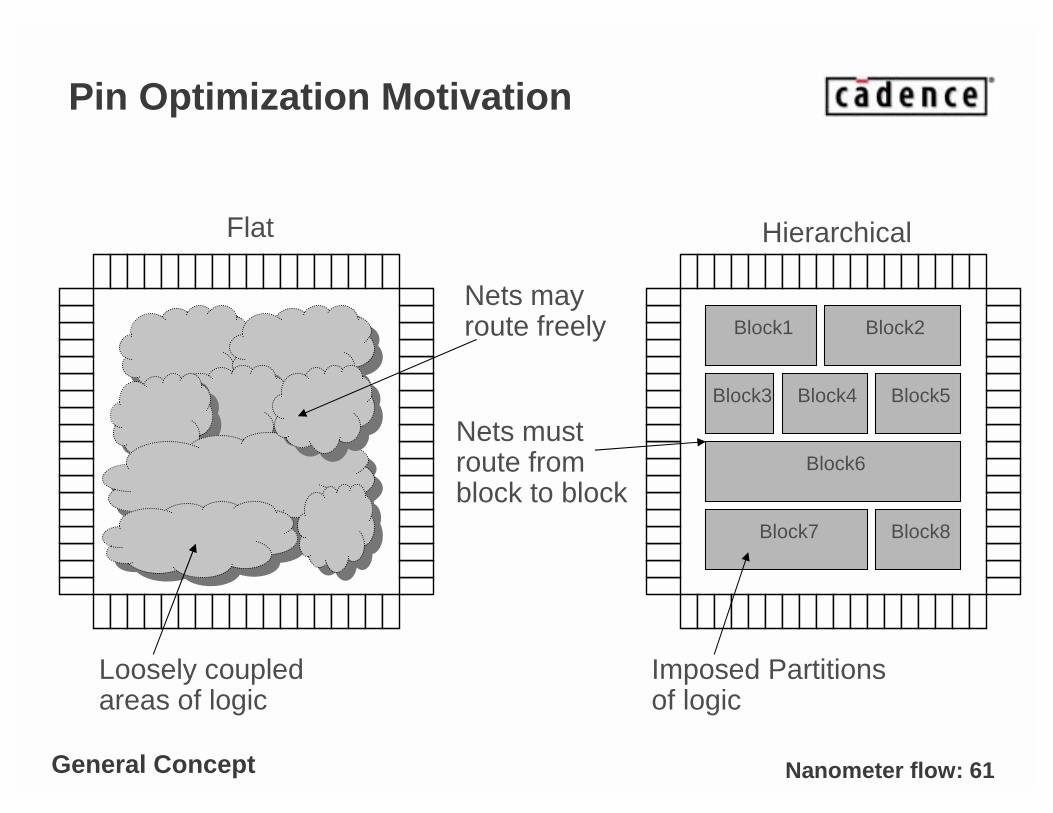
Pin Optimization Motivation
Block1 Block2
Block3 Block5Block4
Block6
Block7 Block8
Flat Hierarchical
Loosely coupled areas of logic
Imposed Partitions of logic
Nets may route freely
Nets must route from block to block
General Concept
Nanometer flow: 62
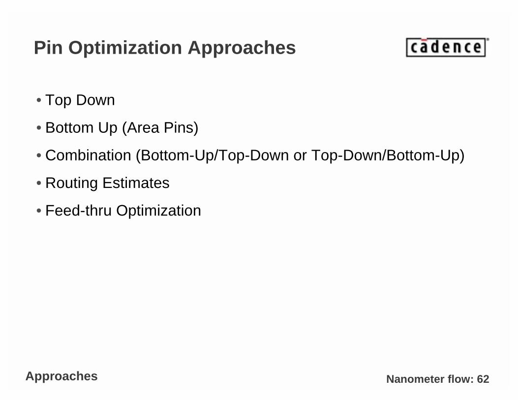
Pin Optimization Approaches
• Top Down
• Bottom Up (Area Pins)
• Combination (Bottom-Up/Top-Down or Top-Down/Bottom-Up)
• Routing Estimates
• Feed-thru Optimization
Approaches
Nanometer flow: 63
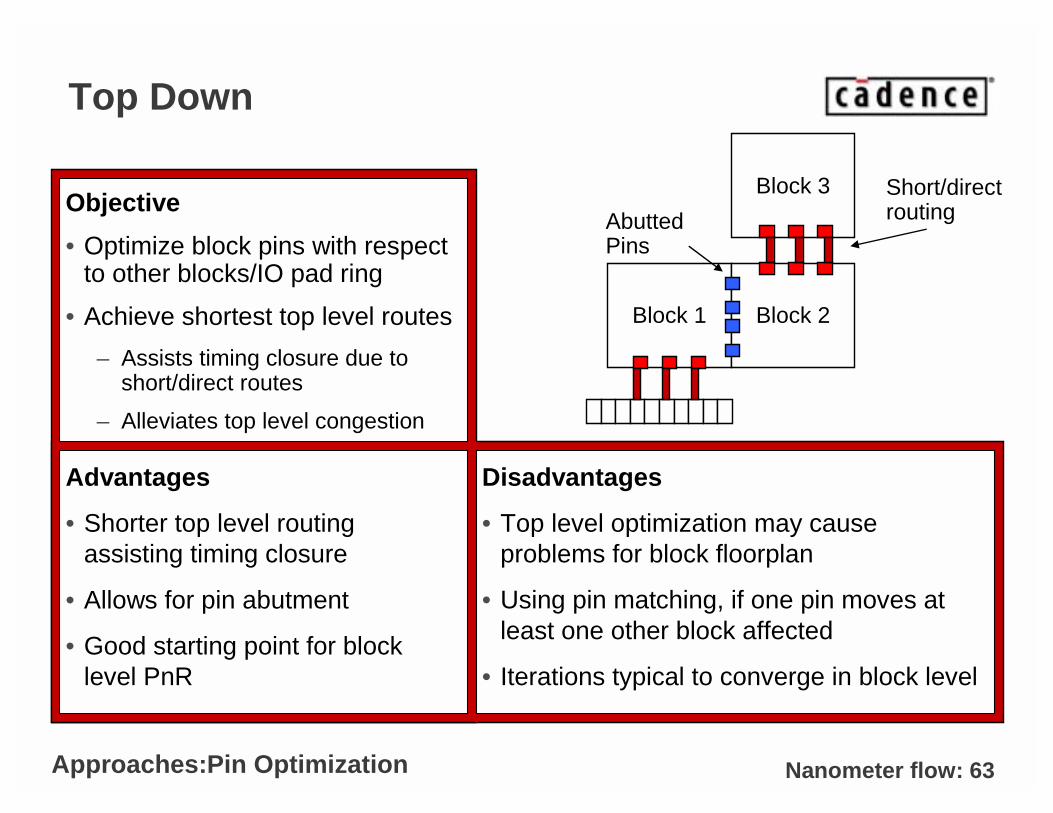
Top Down
Objective
• Optimize block pins with respect to other blocks/IO pad ring
• Achieve shortest top level routes
– Assists timing closure due to short/direct routes
– Alleviates top level congestion
Advantages
• Shorter top level routing assisting timing closure
• Allows for pin abutment
• Good starting point for block level PnR
Disadvantages
• Top level optimization may cause problems for block floorplan
• Using pin matching, if one pin moves at least one other block affected
• Iterations typical to converge in block level
Block 1 Block 2
Short/direct routing
Block 3
Abutted Pins
Approaches:Pin Optimization
Nanometer flow: 64
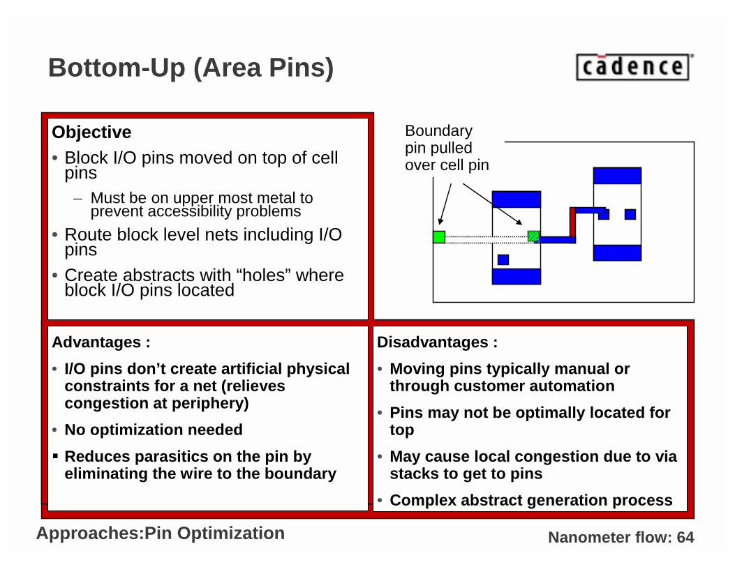
Bottom-Up (Area Pins)
Objective• Block I/O pins moved on top of cell
pins– Must be on upper most metal to
prevent accessibility problems
• Route block level nets including I/O pins
• Create abstracts with “holes” where block I/O pins located
Boundary pin pulled over cell pin
Approaches:Pin Optimization
Advantages :
• I/O pins don’t create artificial physical constraints for a net (relieves congestion at periphery)
• No optimization needed
� Reduces parasitics on the pin by eliminating the wire to the boundary
Disadvantages :
• Moving pins typically manual or through customer automation
• Pins may not be optimally located for top
• May cause local congestion due to via stacks to get to pins
• Complex abstract generation process
Nanometer flow: 65
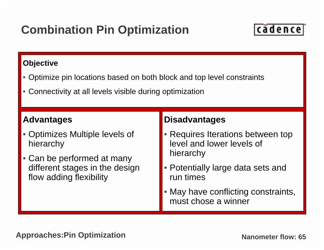
Combination Pin Optimization
Advantages
• Optimizes Multiple levels of hierarchy
• Can be performed at many different stages in the design flow adding flexibility
Disadvantages
• Requires Iterations between top level and lower levels of hierarchy
• Potentially large data sets and run times
• May have conflicting constraints, must chose a winner
Approaches:Pin Optimization
Objective
• Optimize pin locations based on both block and top level constraints
• Connectivity at all levels visible during optimization
Nanometer flow: 66
Routing Estimates
Objective
• Assign pin locations based on a global routing information from flat prototyping
• Prototyping Steps– Perform flat placement of entire design
– Physical partitioning (block boundaries are created)– Obtain global routing plan
– Pins are placed where global routes intersect block boundaries
Approaches:Pin Optimization
Advantages
• All block pins locations are derived and optimized concurrently
• Routability/congestion tested
Disadvantages
• Run times may be high, especially when blocks need to change
• Global routes must correlate with final implementation
Nanometer flow: 67
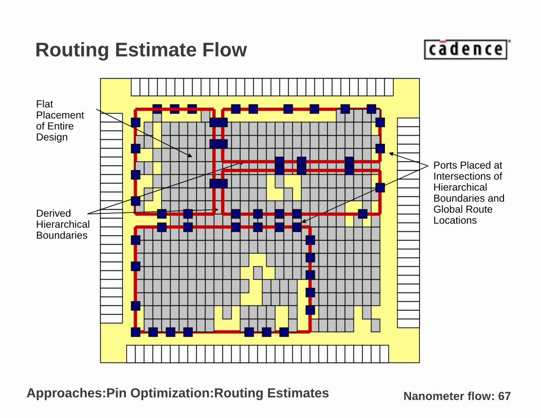
Routing Estimate Flow
Flat Placement of Entire Design
Derived Hierarchical Boundaries
Ports Placed at Intersections of Hierarchical Boundaries and Global Route Locations
Approaches:Pin Optimization:Routing Estimates
CADENCE CONFIDENTIAL
Power Distribution(Can be skipped in a first class)
Through the flow step by step
Nanometer flow: 69
Overview
• Motivation
– Create a power grid distribution system to ensure all transistors in the design have a sufficient and reliable source of power
• General Power Distribution Concepts
– Design Requirements
– overlapping power structures
– connections to analog blocks
– IO pad issues
– metal slotting
• Approaches
– Trunks and rings over entire chip
– Uniform chip grid
– Bottom-up grid generation
Overview
Nanometer flow: 70
Choosing a Power Distribution Strategy
• Understand the system requirements
– Different package types can affect the implementation– Flip-chip vs. Wire Bond
– Number of I/O dedicated to power and ground– Fewer pads require a lower resistance grid (denser)
• Understand the power budget
– Chips consuming significant power require robust strategies
• Understand the tolerable IR Drop and Ground Bounce limits
• Special floorplan considerations
– large macros blocking areas of the chip
• Approaches
– Trunk and Rings
– Uniform Grid
– Bottom-Up
Approaches
Nanometer flow: 71
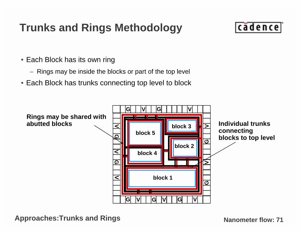
Trunks and Rings Methodology
• Each Block has its own ring
– Rings may be inside the blocks or part of the top level
• Each Block has trunks connecting top level to block
V GG V
block 2
block 1
block 3block 5
block 4
VV
VG
G
GV
VG
V V VGG G
Individual trunks connecting blocks to top level
Rings may be shared with abutted blocks
Approaches:Trunks and Rings

Nanometer flow: 72
Trunks and Rings
Advantages
• Power tailored to the demands of each block (flexible)
• More area efficient since the demands of each block are uniquely met
• Simple implementation supported by many tools
• Rings can be shared between blocks by abutted blocks
Disadvantages
• Limited redundancy, power grid built to match needs
– Assumptions in design may change or be invalid
• Non regular structure requires more detailed IR drop/EM analysis
– missing vias/connections fatal
• Rings will require slotting/splitting due to wide widths
– Increase in data volume
Approaches:Trunks and Rings
Nanometer flow: 73
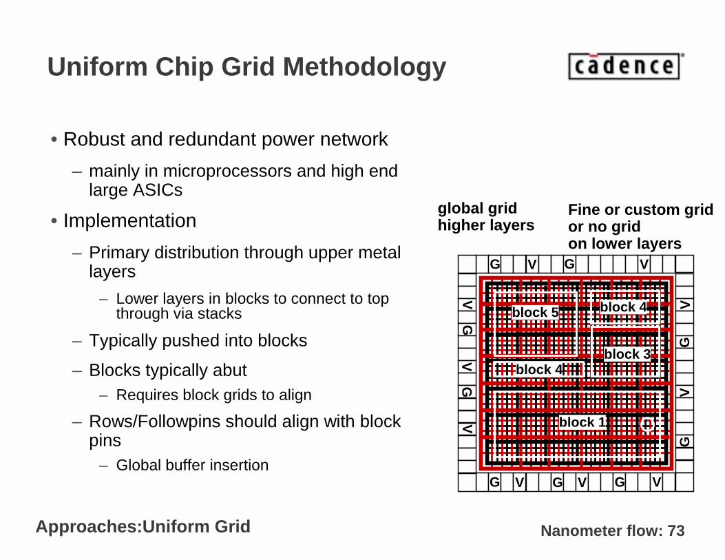
Uniform Chip Grid Methodology
• Robust and redundant power network
– mainly in microprocessors and high end large ASICs
• Implementation
– Primary distribution through upper metal layers
– Lower layers in blocks to connect to top through via stacks
– Typically pushed into blocks
– Blocks typically abut– Requires block grids to align
– Rows/Followpins should align with block pins
– Global buffer insertion
V GG VV
VV
GG
GV
VG
V V VGG G
global gridhigher layers
Fine or custom gridor no gridon lower layers
block 5 block 4
block 3
block 1
block 4
Approaches:Uniform Grid
Nanometer flow: 74
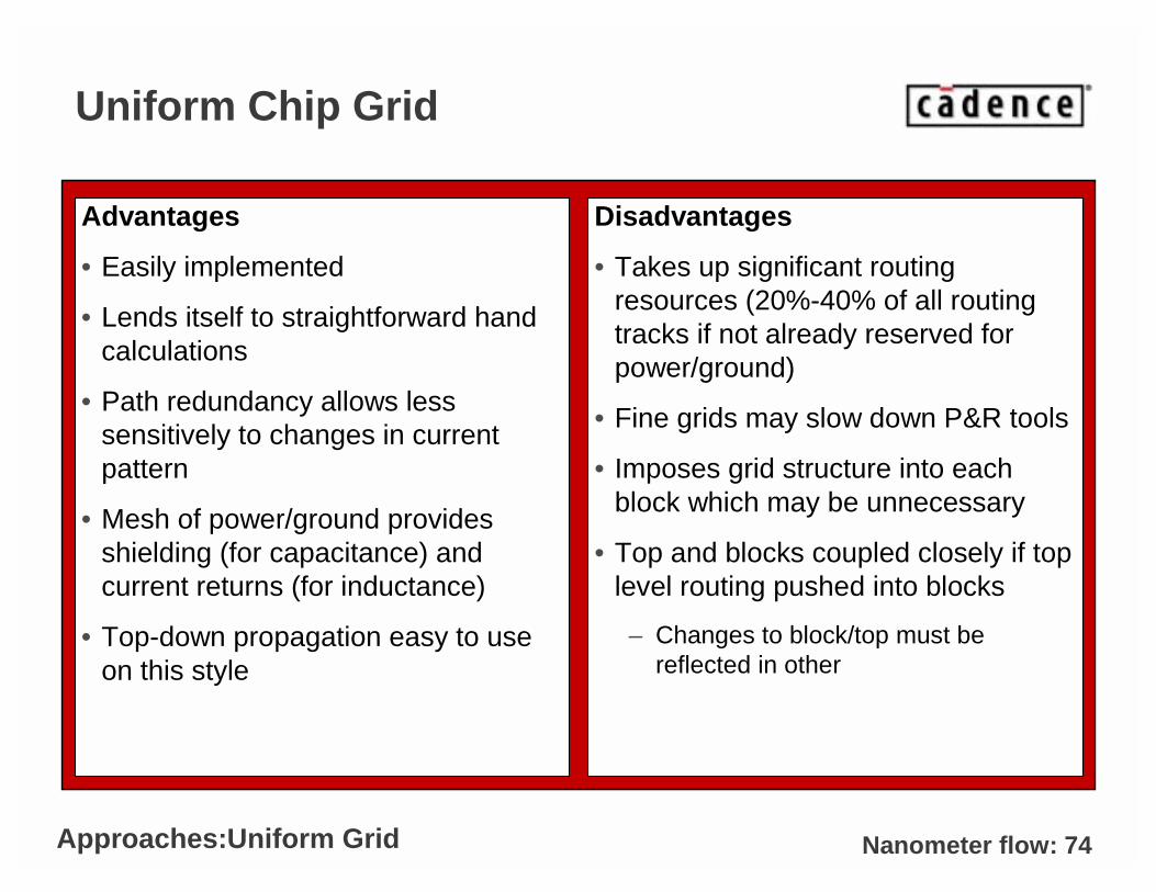
Uniform Chip Grid
Advantages
• Easily implemented
• Lends itself to straightforward hand calculations
• Path redundancy allows less sensitively to changes in current pattern
• Mesh of power/ground provides shielding (for capacitance) and current returns (for inductance)
• Top-down propagation easy to use on this style
Disadvantages
• Takes up significant routing resources (20%-40% of all routing tracks if not already reserved for power/ground)
• Fine grids may slow down P&R tools
• Imposes grid structure into each block which may be unnecessary
• Top and blocks coupled closely if top level routing pushed into blocks
– Changes to block/top must be reflected in other
Approaches:Uniform Grid
Nanometer flow: 75
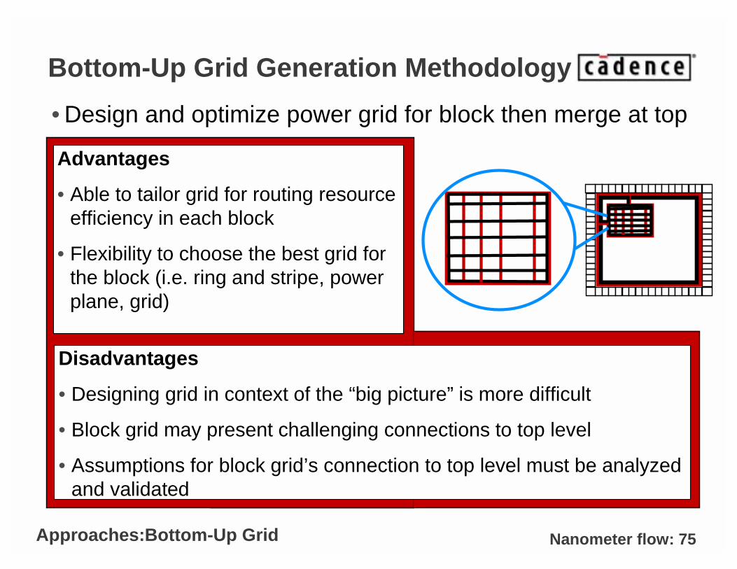
Advantages
• Able to tailor grid for routing resource efficiency in each block
• Flexibility to choose the best grid for the block (i.e. ring and stripe, power plane, grid)
Bottom-Up Grid Generation Methodology
• Design and optimize power grid for block then merge at top
Disadvantages
• Designing grid in context of the “big picture” is more difficult
• Block grid may present challenging connections to top level
• Assumptions for block grid’s connection to top level must be analyzed and validated
Approaches:Bottom-Up Grid
Nanometer flow: 76
Power Distribution Summary
• Ring and trunk – medium to small ASIC, efficient routing
• Uniform grid – redundant power but lower routing efficiency
• Bottom-up – custom power each block, integrate at top
• IR drop pattern critically affected by pad location
• Recommendations
– Uniform grid with global distribution on higher layer metals
– Using splitting over slotting to satisfy slotting rules aids in the implementation/analysis
– Watch width mismatches at interfaces of macros and I/O
– Verify all grids with power grid analysis
Summary
CADENCE CONFIDENTIAL
Hierarchical Clock Distribution
Through the flow step by step
Nanometer flow: 78
Overview
• Motivation
– Create a full chip clock distribution network that meets performance targets while consuming the minimum power, area and routing resources
• General Clock Distribution Concepts
– Clock net characteristics
– Duty Cycle
– Insertion Delay and Skew
– Gating
• Approaches
– Synthesized
– Mesh
– Central
Overview
Nanometer flow: 79
Clock Net Characteristics
• Typically have high fanouts
• Span almost the entire chip
• Typically the most active signals on the chip
• Depending on the approach, may be difficult to model/observe in hierarchical designs
• Typically are cross-talk aggressors due to their high switching rates and fast edges
• Typically the largest consumers of power in the design since they toggle every clock cycle
General Concepts
Nanometer flow: 80
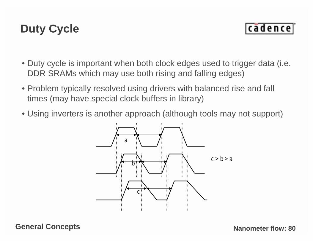
Duty Cycle
• Duty cycle is important when both clock edges used to trigger data (i.e. DDR SRAMs which may use both rising and falling edges)
• Problem typically resolved using drivers with balanced rise and fall times (may have special clock buffers in library)
• Using inverters is another approach (although tools may not support)
a
b
c
c > b > a
General Concepts
Nanometer flow: 81
Skew and Insertion Delay
• Skew is the measure of the difference of delay between the minimum and maximum time it takes the clock to reach the leaf cells
– Typically skew hurts the performance of the design although in some cases it can be used to achieve timing targets (useful skew)
– In hierarchical designs, skew may often be associated with both flop-to-flop delays as well as block-to-block or block-to-flop delays
• Insertion delay is a measure of time it takes the clock to propagate from the root of the tree to the leaf cells
– The difference between the minimum and maximum insertion delays is the skew
– In hierarchical designs, insertion delay becomes a critical ingredient in top level clock tree balancing.
General Concepts
Nanometer flow: 82
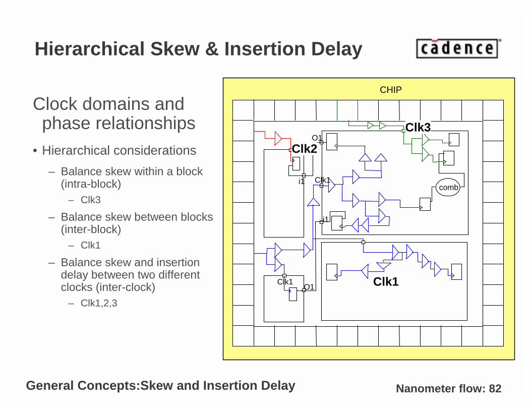
Hierarchical Skew & Insertion Delay
Clock domains and phase relationships
• Hierarchical considerations
– Balance skew within a block (intra-block)
– Clk3
– Balance skew between blocks (inter-block)
– Clk1
– Balance skew and insertion delay between two different clocks (inter-clock)
– Clk1,2,3
CHIP
Clk1
Clk1
O1
i1
i1
O1
comb
Clk1
Clk3
Clk2
General Concepts:Skew and Insertion Delay
Nanometer flow: 83
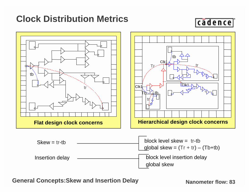
Clock Distribution Metrics
Flat design clock concerns
tr
tb
Hierarchical design clock concerns
Clk1
Clk1
Clk1
tr
tb
Tr
tr
tbTb
Skew = tr-tb block level skew = tr-tbglobal skew = (Tr + tr) – (Tb+tb)
Insertion delay block level insertion delayglobal skew
General Concepts:Skew and Insertion Delay
Nanometer flow: 84
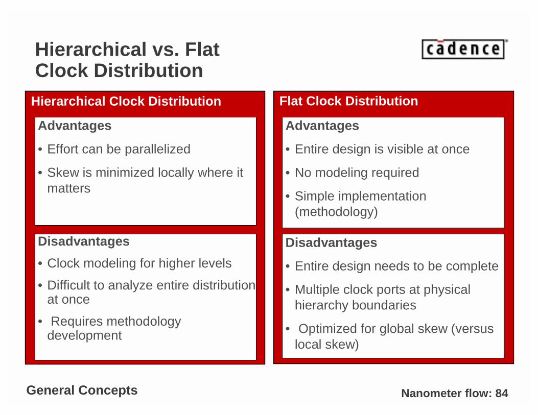
Flat Clock DistributionHierarchical Clock Distribution
Hierarchical vs. FlatClock Distribution
Advantages
• Effort can be parallelized
• Skew is minimized locally where it matters
Disadvantages
• Clock modeling for higher levels
• Difficult to analyze entire distribution at once
• Requires methodology development
General Concepts
Advantages
• Entire design is visible at once
• No modeling required
• Simple implementation (methodology)
Disadvantages
• Entire design needs to be complete
• Multiple clock ports at physical hierarchy boundaries
• Optimized for global skew (versus local skew)
Nanometer flow: 85
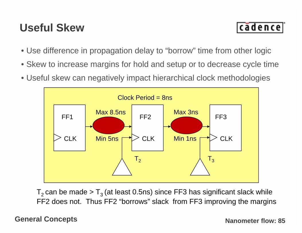
Useful Skew
• Use difference in propagation delay to “borrow” time from other logic
• Skew to increase margins for hold and setup or to decrease cycle time
• Useful skew can negatively impact hierarchical clock methodologies
CLK CLK CLK
Max 8.5ns
Min 5ns
Max 3ns
Min 1ns
Clock Period = 8ns
T2 T3
T2 can be made > T3 (at least 0.5ns) since FF3 has significant slack while FF2 does not. Thus FF2 “borrows” slack from FF3 improving the margins
FF1 FF2 FF3
General Concepts

Nanometer flow: 86
Clock Tree Synthesis (CTS)
Overview
• Match delays at leaf nodes using equivalent receiving loads and interconnect segments
• Commonly implemented using Routing Estimation
Approaches:CTS
Advantages
• Low power compared to mesh
• Supports clock gating
• Distributed power consumption (less temperature gradient in substrate)
Disadvantages
• Netlist changes
• Larger/unpredictable insertion delay and skew
• Sensitive to process/voltage/temp variations
• May alter port connections
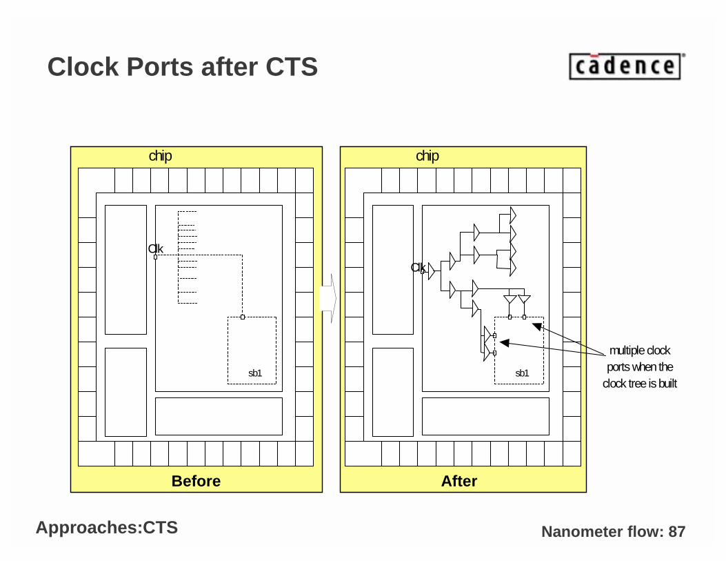
Nanometer flow: 87
Clock Ports after CTS
sb1
chip
multiple clockports when the
clock tree is builtsb1
chip
Clk
Clk
Before After
Approaches:CTS
CADENCE CONFIDENTIAL
Parasitic Extraction
Through the flow step by step
Nanometer flow: 89
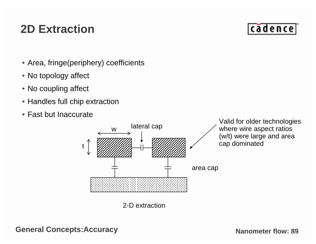
2D Extraction
• Area, fringe(periphery) coefficients
• No topology affect
• No coupling affect
• Handles full chip extraction
• Fast but Inaccurate
2-D extraction
area cap
lateral capValid for older technologies where wire aspect ratios (w/t) were large and area cap dominatedt
w
General Concepts:Accuracy
Nanometer flow: 90
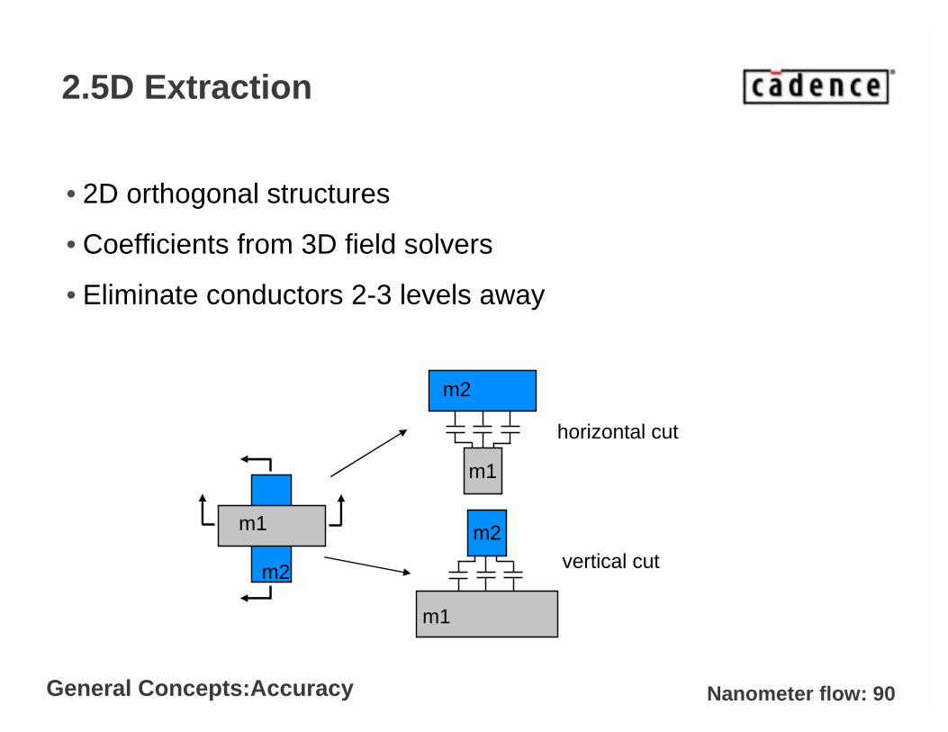
2.5D Extraction
• 2D orthogonal structures
• Coefficients from 3D field solvers
• Eliminate conductors 2-3 levels away
m1
m2vertical cut
horizontal cut
m1
m2
m2
m1
General Concepts:Accuracy
Nanometer flow: 91
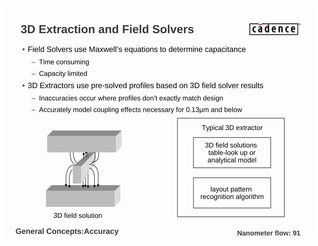
3D Extraction and Field Solvers
• Field Solvers use Maxwell’s equations to determine capacitance
– Time consuming
– Capacity limited
• 3D Extractors use pre-solved profiles based on 3D field solver results
– Inaccuracies occur where profiles don’t exactly match design
– Accurately model coupling effects necessary for 0.13µm and below
3D field solution
3D field solutions table-look up oranalytical model
layout pattern recognition algorithm
Typical 3D extractor
General Concepts:Accuracy
Nanometer flow: 92
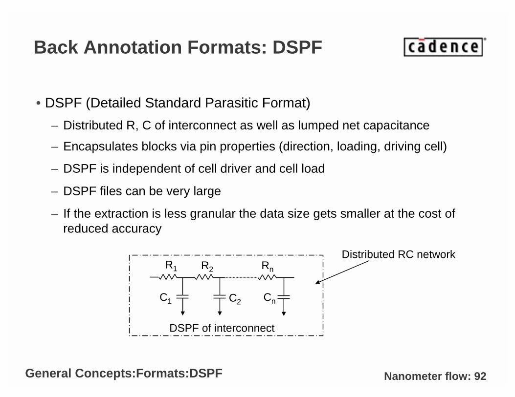
Back Annotation Formats: DSPF
• DSPF (Detailed Standard Parasitic Format)
– Distributed R, C of interconnect as well as lumped net capacitance
– Encapsulates blocks via pin properties (direction, loading, driving cell)
– DSPF is independent of cell driver and cell load
– DSPF files can be very large
– If the extraction is less granular the data size gets smaller at the cost of reduced accuracy
DSPF of interconnect
R1 R2 Rn
C1 C2 Cn
Distributed RC network
General Concepts:Formats:DSPF

Nanometer flow: 93
Back Annotation Formats: RSPF
RSPF (Reduced Standard Parasitic Format)
• Reduced model
– Driver represented by a PI model
– Interconnect loading Elmore
– An order of magnitude smaller than DSPF file
• RSPF reduction is done with known cell driver and known cell load
– Changing drive cell change RSPF
– Necessary to know boundary conditions of design for accurate RSPF
• RSPF of different levels of hierarchy in hierarchical designs can not be combined in simple manner
V
C1 C2
Rπ
RL2
CL2
RSPF of interconnect
V
RL1
CL1
Driver side Loads
General Concepts:Formats:RSPF
Nanometer flow: 94
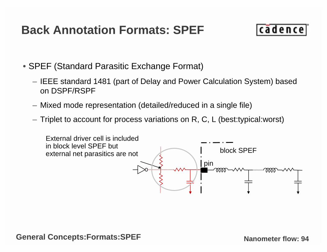
Back Annotation Formats: SPEF
• SPEF (Standard Parasitic Exchange Format)
– IEEE standard 1481 (part of Delay and Power Calculation System) based on DSPF/RSPF
– Mixed mode representation (detailed/reduced in a single file)
– Triplet to account for process variations on R, C, L (best:typical:worst)
External driver cell is included in block level SPEF but external net parasitics are not block SPEF
pin
General Concepts:Formats:SPEF
Nanometer flow: 95
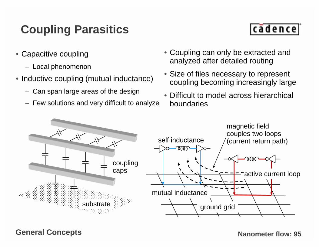
Coupling Parasitics
• Capacitive coupling
– Local phenomenon
• Inductive coupling (mutual inductance)
– Can span large areas of the design
– Few solutions and very difficult to analyze
active current loop
ground grid
mutual inductance
magnetic field couples two loops(current return path)
substrate
couplingcaps
• Coupling can only be extracted and analyzed after detailed routing
• Size of files necessary to represent coupling becoming increasingly large
• Difficult to model across hierarchical boundaries
General Concepts
self inductance
Nanometer flow: 96
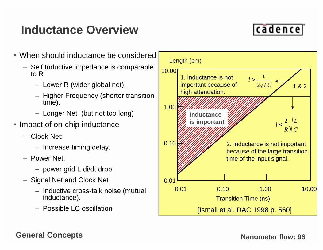
Inductance Overview
• When should inductance be considered
– Self Inductive impedance is comparable to R
– Lower R (wider global net).
– Higher Frequency (shorter transition time).
– Longer Net (but not too long)
• Impact of on-chip inductance
– Clock Net:
– Increase timing delay.
– Power Net:
– power grid L di/dt drop.
– Signal Net and Clock Net
– Inductive cross-talk noise (mutual inductance).
– Possible LC oscillation
10.00
1.00
0.10
0.010.01 0.10 1.00 10.00
Length (cm)
Transition Time (ns)
1 & 21. Inductance is not important because of high attenuation.
2. Inductance is not importantbecause of the large transition time of the input signal.
Inductance is important
LC
tl
r
2>
C
L
Rl
2<
[Ismail et al. DAC 1998 p. 560]
General Concepts
Nanometer flow: 97
Design for Inductance Minimization
• Shielding
– Provides dedicated return path (also path with minimum impedance)
• Wider Wires
– Reduce self inductance
– L reduces 33% when width increases from 1um to 20um
• Delay Optimization
– Insert repeaters to reduce RLC
• Avoid Over-Driving
– Smaller driver R renders inductive impedance more significant
General Concepts:Inductance
CADENCE CONFIDENTIAL
Timing Analysis
Through the flow step by step
Nanometer flow: 99
Static Timing Analysis (STA)
Key Points
• Static timing Analysis
– Uses output of the delay calculation engine
– Uses an analysis/filter engine to report timing
• Fast and accurate path analysis of synchronous designs
– Many asynchronous paths can be handled by additional timing constraints
• Higher order models and their accuracies
• Mixing latch and flop based designs
– time borrowing at hierarchical block boundaries
• Propagated or “ideal” clock mode
• Requires constraints to model paths with timing exceptions
General Concepts
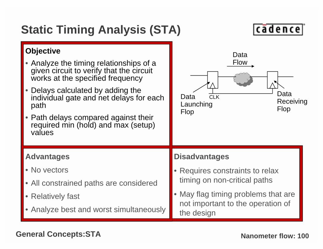
Nanometer flow: 100
Static Timing Analysis (STA)
Objective
• Analyze the timing relationships of a given circuit to verify that the circuit works at the specified frequency
• Delays calculated by adding the individual gate and net delays for each path
• Path delays compared against their required min (hold) and max (setup) values
Advantages
• No vectors
• All constrained paths are considered
• Relatively fast
• Analyze best and worst simultaneously
Disadvantages
• Requires constraints to relax timing on non-critical paths
• May flag timing problems that are not important to the operation of the design
Data Flow
Data Launching Flop
Data Receiving Flop
CLK
General Concepts:STA
Nanometer flow: 101
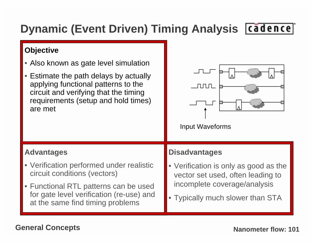
Dynamic (Event Driven) Timing Analysis
Objective
• Also known as gate level simulation
• Estimate the path delays by actually applying functional patterns to the circuit and verifying that the timing requirements (setup and hold times) are met
Advantages
• Verification performed under realistic circuit conditions (vectors)
• Functional RTL patterns can be used for gate level verification (re-use) and at the same find timing problems
Disadvantages
• Verification is only as good as the vector set used, often leading to incomplete coverage/analysis
• Typically much slower than STA
Input Waveforms
General Concepts
Nanometer flow: 102
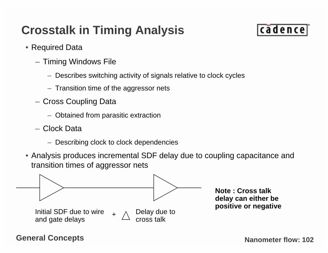
Crosstalk in Timing Analysis• Required Data
– Timing Windows File
– Describes switching activity of signals relative to clock cycles
– Transition time of the aggressor nets
– Cross Coupling Data
– Obtained from parasitic extraction
– Clock Data
– Describing clock to clock dependencies
• Analysis produces incremental SDF delay due to coupling capacitance and transition times of aggressor nets
Initial SDF due to wire and gate delays
+ Delay due to cross talk
Note : Cross talk delay can either be positive or negative
General Concepts
Nanometer flow: 103
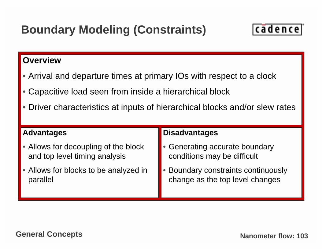
Boundary Modeling (Constraints)
Overview
• Arrival and departure times at primary IOs with respect to a clock
• Capacitive load seen from inside a hierarchical block
• Driver characteristics at inputs of hierarchical blocks and/or slew rates
General Concepts
Advantages
• Allows for decoupling of the block and top level timing analysis
• Allows for blocks to be analyzed in parallel
Disadvantages
• Generating accurate boundary conditions may be difficult
• Boundary constraints continuously change as the top level changes

Nanometer flow: 104
Modeling Block to Block Paths
3ns
Resulting Boundary Constraints
Departure Time = 3ns Arrival Time = 4ns
2ns
Given a clock frequency of 6ns
1ns
General Concepts:Boundary Constraints
Nanometer flow: 105
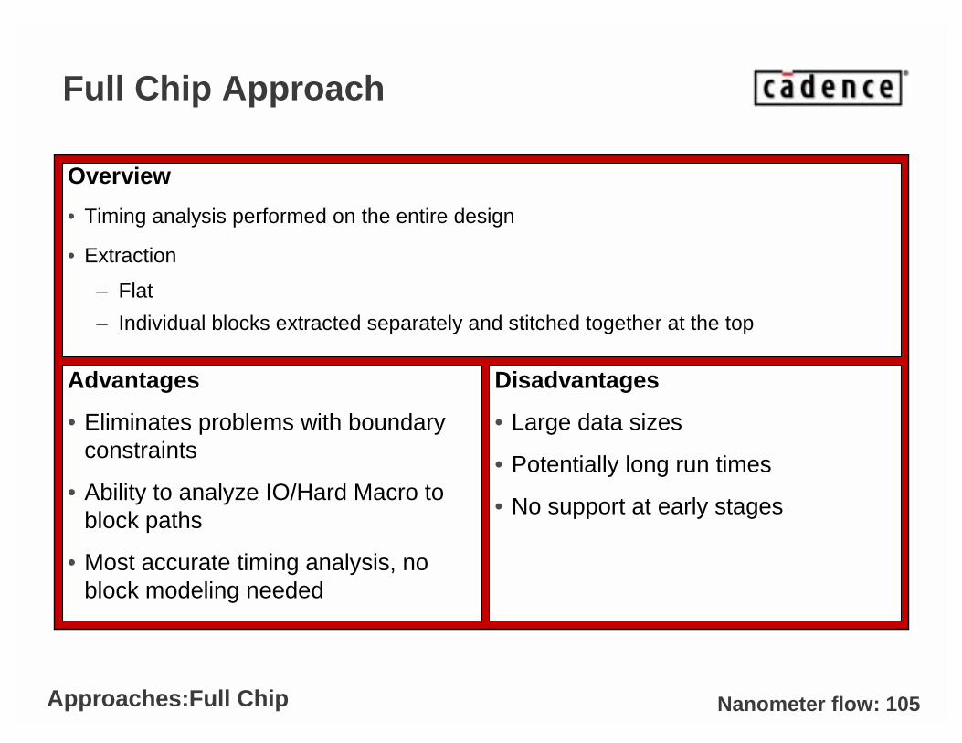
Full Chip Approach
Overview
• Timing analysis performed on the entire design
• Extraction
– Flat
– Individual blocks extracted separately and stitched together at the top
Approaches:Full Chip
Advantages
• Eliminates problems with boundary constraints
• Ability to analyze IO/Hard Macro to block paths
• Most accurate timing analysis, no block modeling needed
Disadvantages
• Large data sizes
• Potentially long run times
• No support at early stages
Nanometer flow: 106
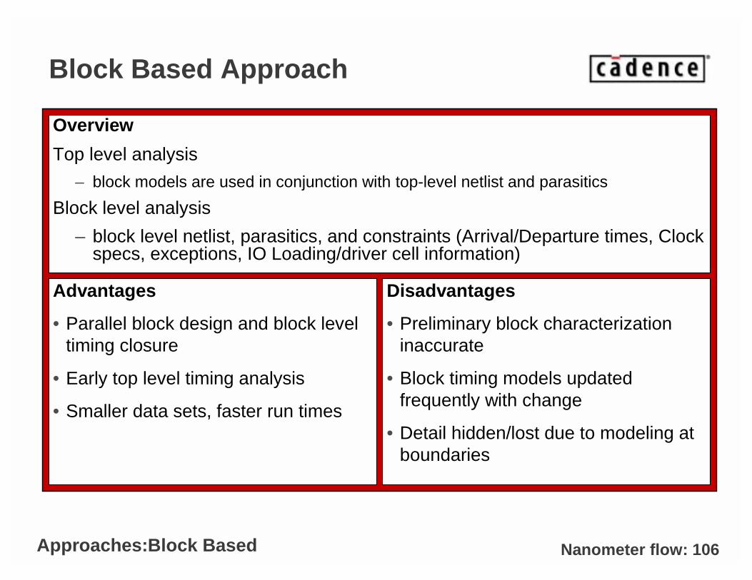
Block Based Approach
Overview
Top level analysis
– block models are used in conjunction with top-level netlist and parasitics
Block level analysis
– block level netlist, parasitics, and constraints (Arrival/Departure times, Clock specs, exceptions, IO Loading/driver cell information)
Approaches:Block Based
Advantages
• Parallel block design and block level timing closure
• Early top level timing analysis
• Smaller data sets, faster run times
Disadvantages
• Preliminary block characterization inaccurate
• Block timing models updated frequently with change
• Detail hidden/lost due to modeling at boundaries
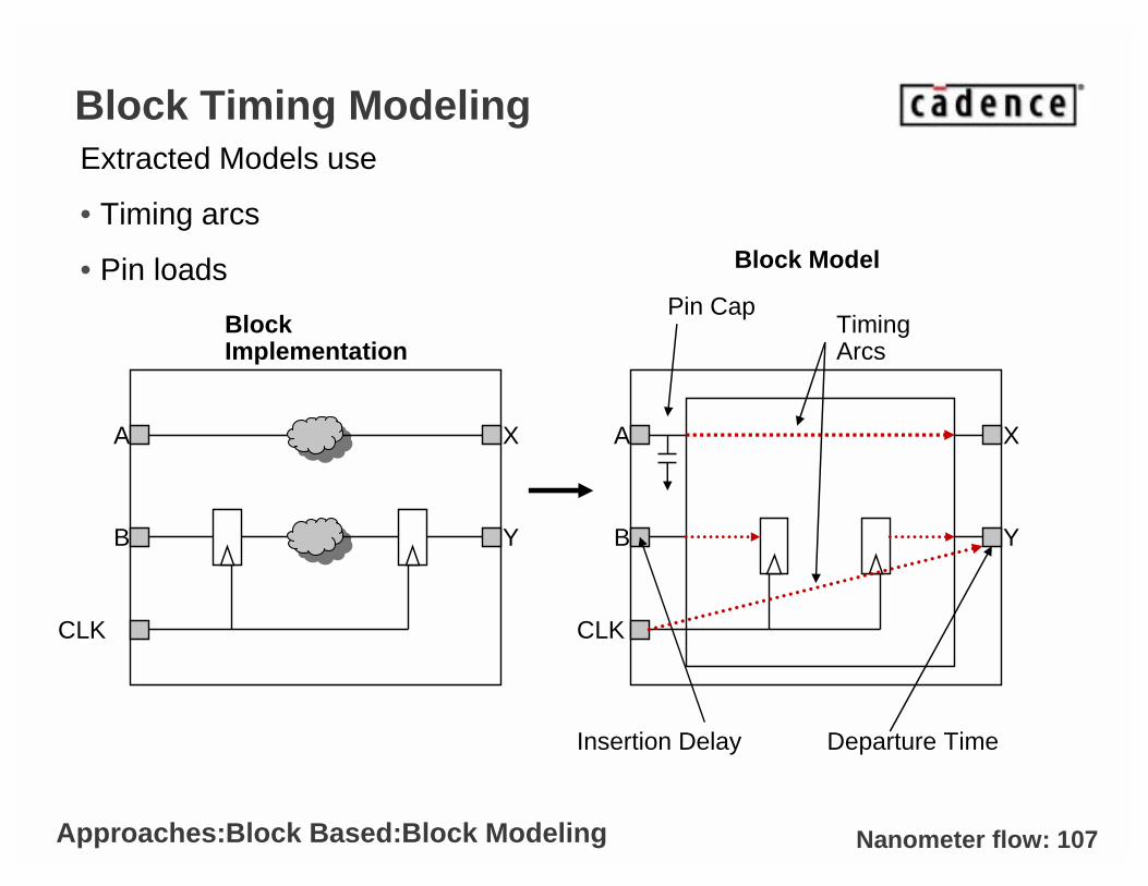
Nanometer flow: 107
Block Timing ModelingExtracted Models use
• Timing arcs
• Pin loads
A
B
CLK
X
Y
A
B
CLK
X
Y
Timing Arcs
Insertion Delay Departure Time
Pin Cap
Approaches:Block Based:Block Modeling
Block Implementation
Block Model
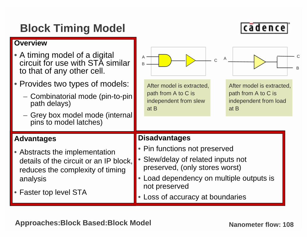
Nanometer flow: 108
Block Timing ModelOverview
• A timing model of a digital circuit for use with STA similar to that of any other cell.
• Provides two types of models:
– Combinatorial mode (pin-to-pin path delays)
– Grey box model mode (internal pins to model latches)
A
BC
After model is extracted,path from A to C isindependent from slewat B
A
B
C
After model is extracted,path from A to C is independent from loadat B
Approaches:Block Based:Block Model
Advantages
• Abstracts the implementation details of the circuit or an IP block, reduces the complexity of timing analysis
• Faster top level STA
Disadvantages• Pin functions not preserved• Slew/delay of related inputs not
preserved, (only stores worst) • Load dependency on multiple outputs is
not preserved• Loss of accuracy at boundaries

CADENCE CONFIDENTIAL
Signal Integrity
Through the flow step by step
Nanometer flow: 110
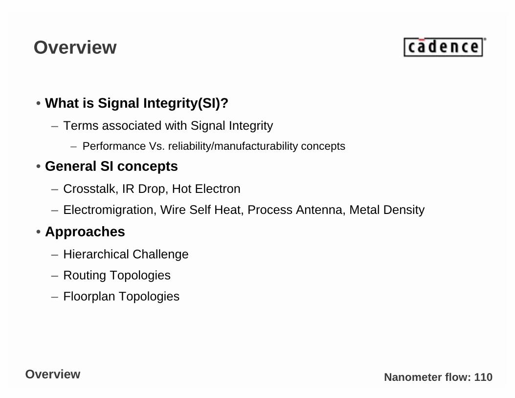
Overview
• What is Signal Integrity(SI)?
– Terms associated with Signal Integrity
– Performance Vs. reliability/manufacturability concepts
• General SI concepts
– Crosstalk, IR Drop, Hot Electron
– Electromigration, Wire Self Heat, Process Antenna, Metal Density
• Approaches
– Hierarchical Challenge
– Routing Topologies
– Floorplan Topologies
Overview
Nanometer flow: 111
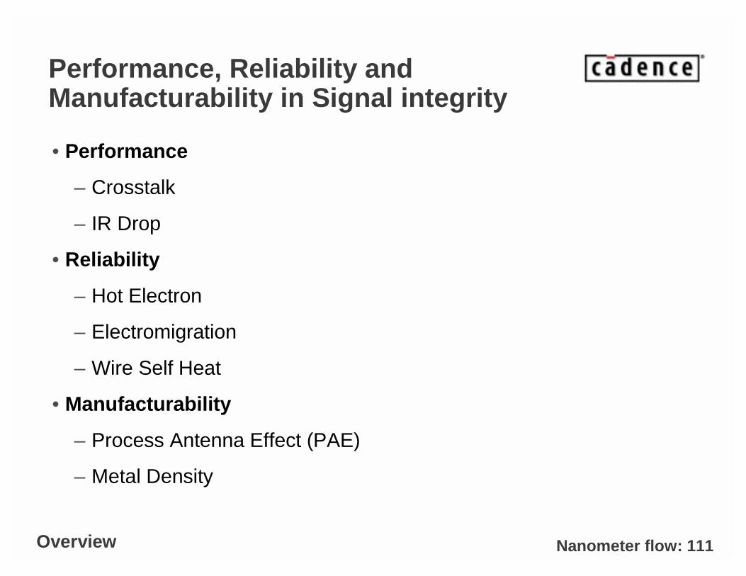
Performance, Reliability and Manufacturability in Signal integrity
• Performance
– Crosstalk
– IR Drop
• Reliability
– Hot Electron
– Electromigration
– Wire Self Heat
• Manufacturability
– Process Antenna Effect (PAE)
– Metal Density
Overview
Nanometer flow: 112
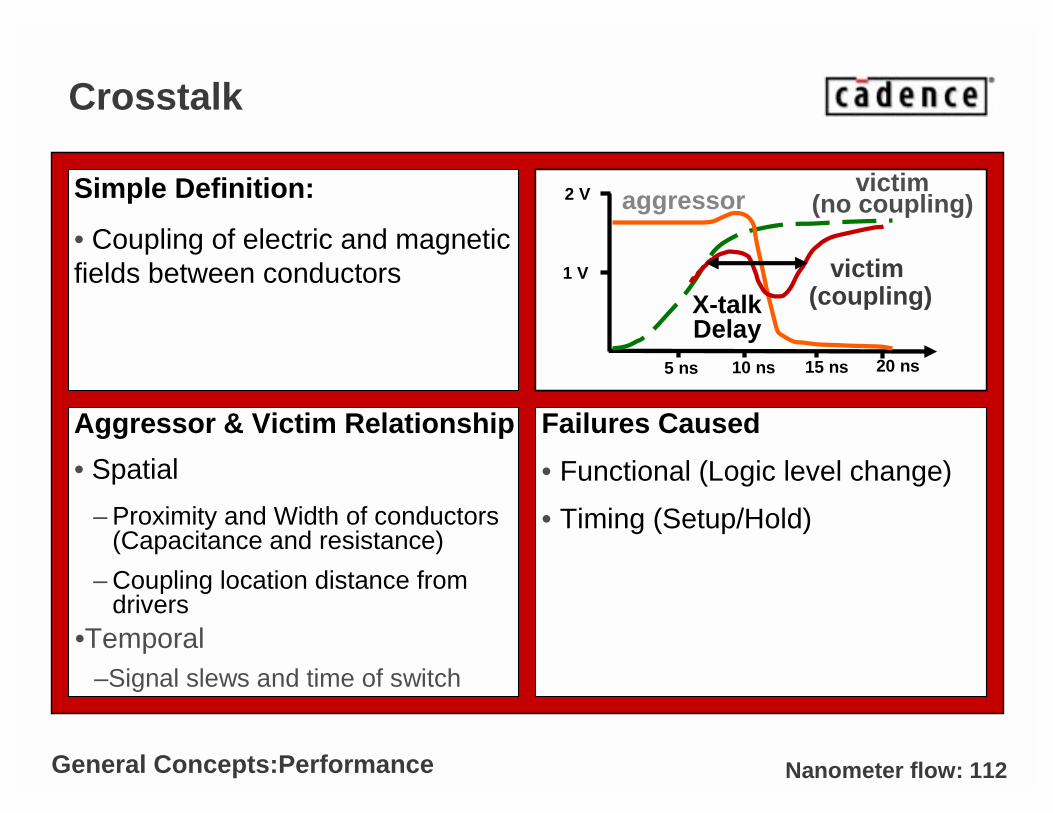
Crosstalk
Aggressor & Victim Relationship
• Spatial
– Proximity and Width of conductors (Capacitance and resistance)
– Coupling location distance from drivers
Failures Caused
• Functional (Logic level change)
• Timing (Setup/Hold)
Simple Definition:
• Coupling of electric and magnetic fields between conductors
General Concepts:Performance
Victim
Victim
Aggressors Coupling
5 ns 15 ns10 ns 20 ns
1 V
2 V victim (no coupling)aggressor
victim (coupling)X-talk
Delay
•Temporal–Signal slews and time of switch
Nanometer flow: 113
Analysis and Avoidance
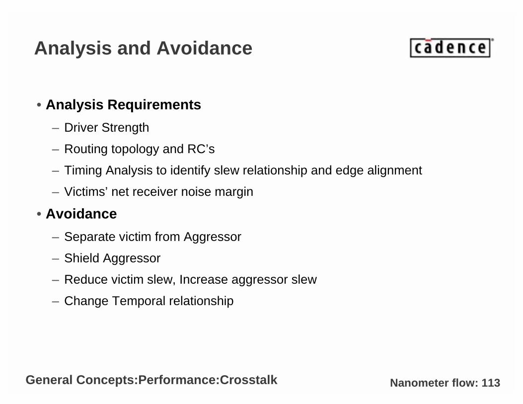
• Analysis Requirements
– Driver Strength
– Routing topology and RC’s
– Timing Analysis to identify slew relationship and edge alignment
– Victims’ net receiver noise margin
• Avoidance
– Separate victim from Aggressor
– Shield Aggressor
– Reduce victim slew, Increase aggressor slew
– Change Temporal relationship
General Concepts:Performance:Crosstalk
Nanometer flow: 114
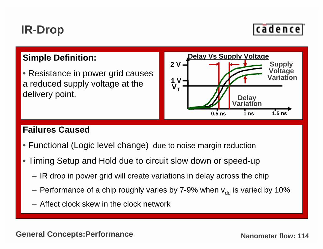
IR-Drop
Failures Caused
• Functional (Logic level change) due to noise margin reduction
• Timing Setup and Hold due to circuit slow down or speed-up
– IR drop in power grid will create variations in delay across the chip
– Performance of a chip roughly varies by 7-9% when vdd is varied by 10%
– Affect clock skew in the clock network
Simple Definition:
• Resistance in power grid causes a reduced supply voltage at the delivery point.
General Concepts:Performance
�V = IR Vdd R
Vss
R
I Vdd- �V
CL
Delay Vs Supply Voltage
0.5 ns 1.5 ns1 ns
1 V
2 V
VT
Supply Voltage Variation
DelayVariation
Nanometer flow: 115
Analysis and Avoidance
• Analysis Requirements
– IR Drop characterization of cells
– Power supply network RC’s extraction
– Estimation of current drawn by each cell
– Supply voltage calculation at each cell
• Avoidance
– General estimation of power network using average current drawn per cell and row utilization.
– Network resistance reduction (adding via cuts and increasing or tapering wire width)
– Establishing max transition time for whole chip.
– Insertion of decoupling caps.
General Concepts:Performance:IR-Drop

Nanometer flow: 116
Hot Electron Effect on Devices
Failures Caused
• Functional
– Eventual device failure
• Timing
– Threshold and mobility shifts.
– Device operates out-of-spec (timing characteristics change)
Simple Definition:
• Process are reducing transistor feature sizes (W/L) faster than supply voltage. Electrons in the channel are damaging the drain and gate oxide.
General Concepts:Reliability
+++
+++
Oxide and/or interfaceis damaged here
Impact ionizationoccurs here

Nanometer flow: 117
Analysis and Avoidance
• Analysis Requirements
– Fluence cell characterization (Flux of injected hot e- [coulomb/m2])
– Chip lifetime estimation
– Number of transitions per cycle
• Avoidance
– Upsize driver (i.e., improve slew)
– Insert buffer (i.e., reduce load)
– Process control (Proportional reduction of supply voltage with feature size.)
General Concepts:Reliability:Hot Electron
Nanometer flow: 118
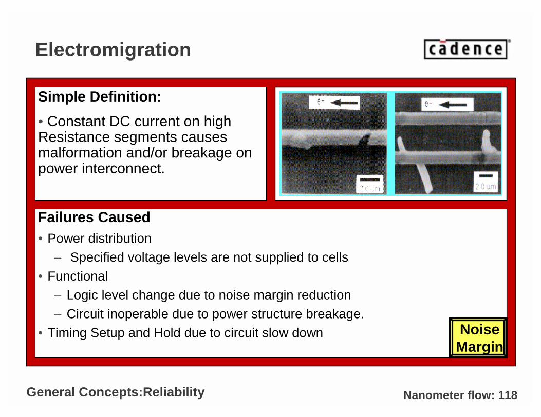
Electromigration
Failures Caused• Power distribution
– Specified voltage levels are not supplied to cells• Functional
– Logic level change due to noise margin reduction– Circuit inoperable due to power structure breakage.
• Timing Setup and Hold due to circuit slow down
Simple Definition:
• Constant DC current on high Resistance segments causes malformation and/or breakage on power interconnect.
General Concepts:Reliability
NoiseMargin
Nanometer flow: 119
Analysis and Avoidance
• Analysis Requirements
– Characterization of cells’ current consumption
– Power supply network RC’s extraction
– Wire DC and peak current densities based on the current consumption of each cell and the resistance of the power grid.
– DC current densities are compared to the process limits.
• Avoidance
– General estimation of power network using DC or average DC current drawn per cell and row utilization.
– Network resistance reduction (adding via cuts and increasing or
tapering wire width).
General Concepts:Reliability:Electromigration
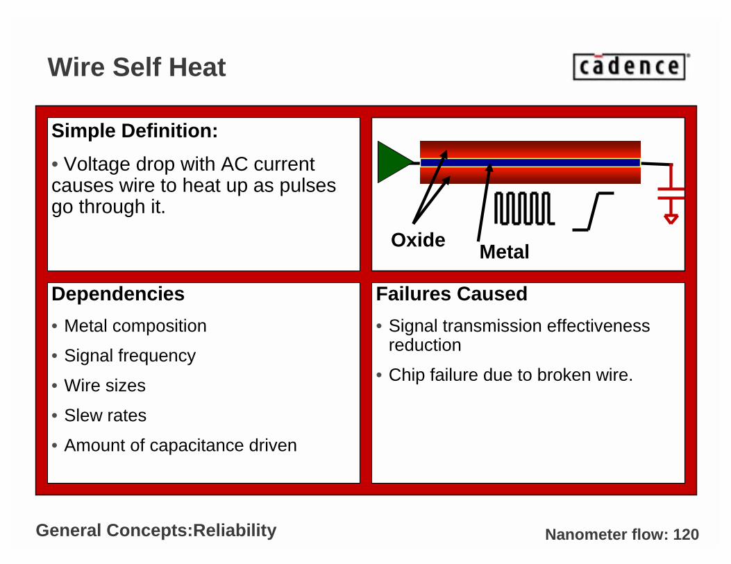
Nanometer flow: 120
Wire Self Heat
Dependencies
• Metal composition
• Signal frequency
• Wire sizes
• Slew rates
• Amount of capacitance driven
Simple Definition:
• Voltage drop with AC current causes wire to heat up as pulses go through it.
General Concepts:Reliability
Metal
Failures Caused
• Signal transmission effectiveness reduction
• Chip failure due to broken wire.
Oxide
Nanometer flow: 121
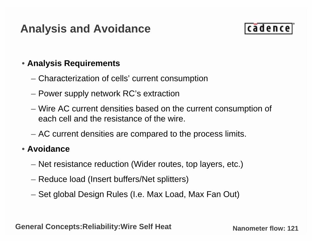
Analysis and Avoidance
• Analysis Requirements
– Characterization of cells’ current consumption
– Power supply network RC’s extraction
– Wire AC current densities based on the current consumption of each cell and the resistance of the wire.
– AC current densities are compared to the process limits.
• Avoidance
– Net resistance reduction (Wider routes, top layers, etc.)
– Reduce load (Insert buffers/Net splitters)
– Set global Design Rules (I.e. Max Load, Max Fan Out)
General Concepts:Reliability:Wire Self Heat
Nanometer flow: 122
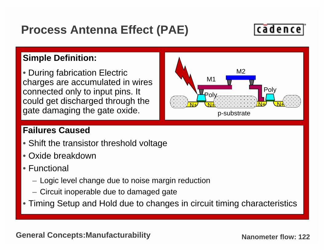
Process Antenna Effect (PAE)
Failures Caused• Shift the transistor threshold voltage• Oxide breakdown• Functional
– Logic level change due to noise margin reduction– Circuit inoperable due to damaged gate
• Timing Setup and Hold due to changes in circuit timing characteristics
Simple Definition:
• During fabrication Electric charges are accumulated in wires connected only to input pins. It could get discharged through the gate damaging the gate oxide.
General Concepts:Manufacturability
p-substrate
FOX
M1M2
PolyN+N+N+N+
Poly
Nanometer flow: 123
Analysis and Avoidance
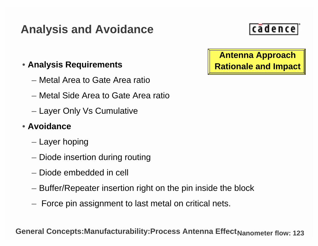
• Analysis Requirements
– Metal Area to Gate Area ratio
– Metal Side Area to Gate Area ratio
– Layer Only Vs Cumulative
• Avoidance
– Layer hoping
– Diode insertion during routing
– Diode embedded in cell
– Buffer/Repeater insertion right on the pin inside the block
– Force pin assignment to last metal on critical nets.
General Concepts:Manufacturability:Process Antenna Effect
Antenna ApproachRationale and Impact
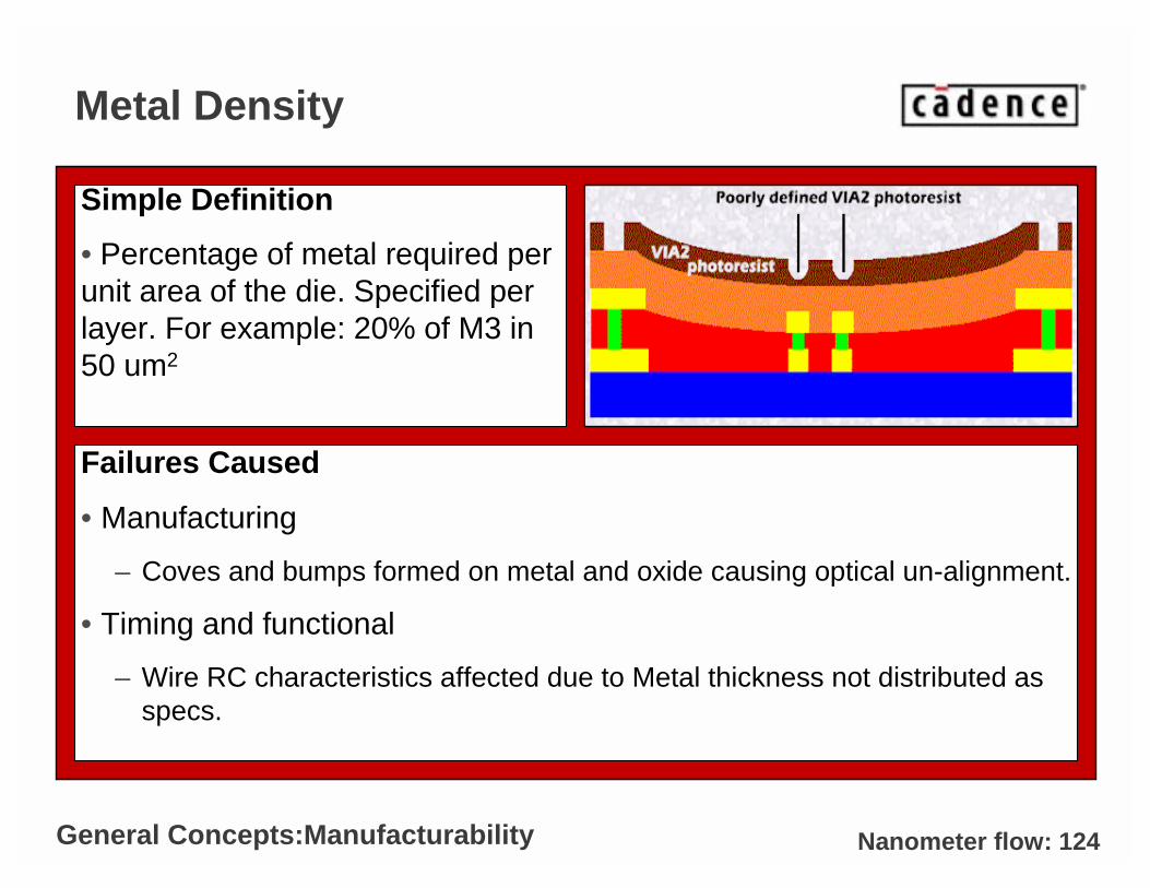
Nanometer flow: 124
Failures Caused
• Manufacturing
– Coves and bumps formed on metal and oxide causing optical un-alignment.
• Timing and functional
– Wire RC characteristics affected due to Metal thickness not distributed as specs.
Metal Density
Simple Definition
• Percentage of metal required per unit area of the die. Specified per layer. For example: 20% of M3 in 50 um2
General Concepts:Manufacturability
Nanometer flow: 125
Analysis and Avoidance
• Analysis Requirements
– Metal utilization per square area.
• Avoidance
– Metal fills are added to satisfy minimum density rules.
– Wires are split or slotted to satisfy the maximum density rules.
– Fixed as a post process of the placed and routed database or the GDSII database.
– Started to be fixed in the place and route environment due to itimplications on RC extraction, Timing Analysis, Signal Integrity, etc.
General Concepts:Manufacturability:Metal Density
CADENCE CONFIDENTIAL
Power Analysis
Through the flow step by step
Nanometer flow: 127
CMOS Power Components
• Static power.
– Leakage power – power consumed when cells are not switching.
• Dynamic power.
– Internal power – power consumed in the cell. Caused by charging internal nodes.
– Short circuit power – power consumed when both N and P devices are open at the same time. Current path established from power rail to ground. It is a function of output load and input slew.
– Switching power – power consumed through charge and discharge of output load.
General Concepts
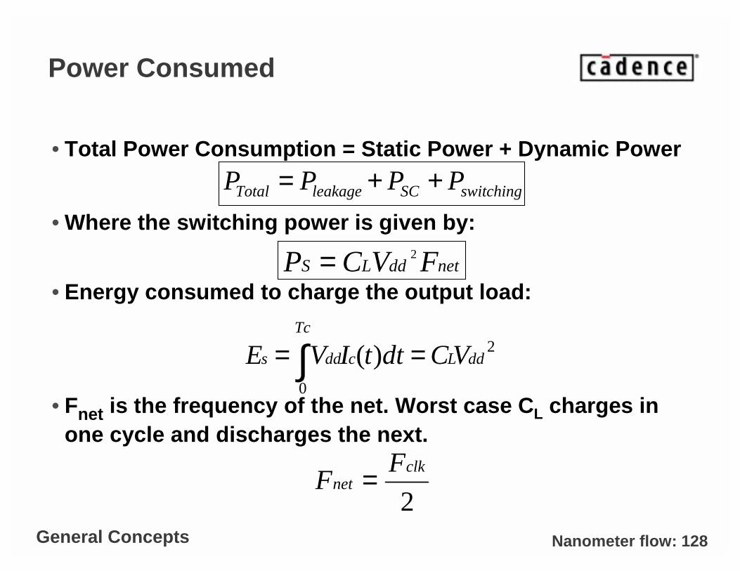
Nanometer flow: 128
Power Consumed
• Total Power Consumption = Static Power + Dynamic Power
• Where the switching power is given by:
• Energy consumed to charge the output load:
• Fnet is the frequency of the net. Worst case CL charges in one cycle and discharges the next.
General Concepts
switchingSCleakageTotal PPPP ++=
2
0
)( dd
Tc
Lcdds VCdttIVE ∫ ==
netddLS FVCP 2=
2
clknet
FF =
Nanometer flow: 129
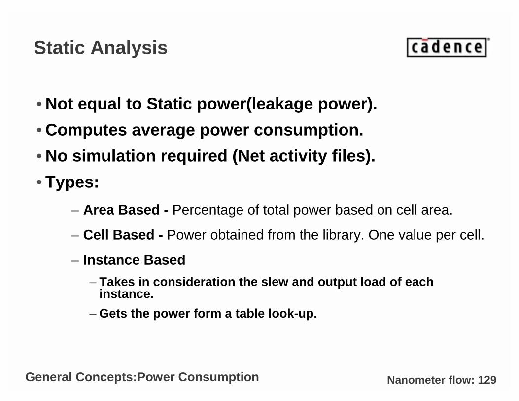
Static Analysis
• Not equal to Static power(leakage power).
• Computes average power consumption.
• No simulation required (Net activity files).
• Types:
– Area Based - Percentage of total power based on cell area.
– Cell Based - Power obtained from the library. One value per cell.
– Instance Based
– Takes in consideration the slew and output load of each instance.
– Gets the power form a table look-up.
General Concepts:Power Consumption
Nanometer flow: 130
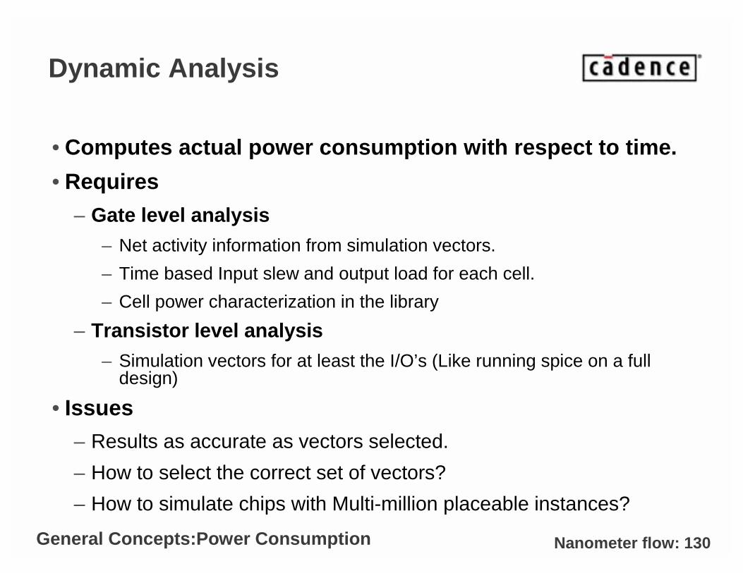
Dynamic Analysis
• Computes actual power consumption with respect to time.
• Requires
– Gate level analysis– Net activity information from simulation vectors.
– Time based Input slew and output load for each cell.
– Cell power characterization in the library
– Transistor level analysis– Simulation vectors for at least the I/O’s (Like running spice on a full
design)
• Issues
– Results as accurate as vectors selected.
– How to select the correct set of vectors?
– How to simulate chips with Multi-million placeable instances?
General Concepts:Power Consumption
CADENCE CONFIDENTIAL
Conclusion
What have we learned
Nanometer flow: 132
What have we learned
• Concepts:– Netlist, Parasitics, cross coupling, IR Drop, Floorplanning, Signal integrity,
Silicon Virtual prototype
• Characteristic of 90nm design– Chip design process focuses on Wire design.
• Tools– History: From Synthesis to Physical Synthesis and to Virtual Prototyping.
– Extraction
– Timing analysis.
• Flow– From RTL to GDSII: Wire first.
– Continuous convergence.
Nanometer flow: 133
If you want to know more
• Practice:
– Flow : Start from RTL or a netlist run synthesis, place and route, extraction, timing verification.
– Tools, accuracy: compare Spice run to timing analysis.
• Internship in Cadence
– Software developer
– Product validation engineer
• Continuous learning experience: 90nm design process will become obsolete before you master it.
• QUESTIONS ? Mail me : [email protected]