isolated ac-dc converter with pfc - vicor corporation · s c us cu nrtl s ® pfm™ in a via...
TRANSCRIPT

S
NRTLC USC US®
PFM™ in a VIA Package Rev 1.0Page 1 of 25 11/2017
PFM™ in a VIA PackageAC-DC Converter
Isolated AC-DC Converter with PFC
PFM4414xB6M48D0yAz
Size:4.35 x 1.40 x .37in110.6 x 35.5 x 9.3mm
Part Ordering Information
ProductFunction
Package Length
PackageWidth
PackageType
Input Voltage
Range Ratio
Output Voltage (Range)
Max Output Power
Product Grade Option Field
PFM 44 14 x B6 M 48 D0 y z z
PFM =Power Factor
Module
Length in Inches x 10
Width in Inches x 10
B = Board VIAV = Chassis VIA
Internal ReferenceC = –20 to 100°CT = –40 to 100°C
A0 = Chassis/Always OnA4 = Short Pin/Always OnA8 = Long Pin/Always On
Features & Benefits
• Universal input (85 – 264VAC)
• 48V output, regulated, isolated SELV
• 92% typical efficiency
• Built-in EMI filtering
• Chassis mount or board mount packaging options
• Always-on, self-protecting converter control architecture
• SELV Output
• Two temperature grades including operation to –40°C
• VIA Package
• Robust Mechanical Design
• Versatile thermal management capability
• Safe and reliable secondary-side energy storage
• High MTBF
• 140W/in3 power density
• 4414 package
• AC Input Front-End Module provides external rectification and transient protection (VIA AIM™ sold separately)
Typical Applications
• Small cell base stations
• Telecom switching equipment
• LED lighting
• Industrial power systems
Product Description
The PFM in a VIA™ Package is a highly advanced 400W AC-DC converter operating from a rectified universal AC input which delivers an isolated and regulated Safety Extra Low Voltage (SELV) 48V secondary output.
This unique, ultra-low profile module incorporates AC-DC conversion, integrated filtering and transient surge protection in a chassis mount or PCB mount form factor.
The PFM enables a versatile two-sided thermal strategy which greatly simplifies thermal design challenges.
When combined with downstream Vicor DC-DC conversion components and regulators, the PFM allows the Power Design Engineer to employ a simple, low-profile design which will differentiate his end-system without compromising on cost or performance metrics.
Product Ratings
VIN = 85 – 264V POUT = up to 400W
VOUT = 48V IOUT = 8.33A
Shown with required companion component, VIA AIM (see pages 2-3)
PFM™ in a VIA Package Rev 1.0Page 2 of 25 11/2017
PFM4414xB6M48D0yAz
48 V 5 A
3.3 V 10 A
1.8 V 8 A
Cool-Power®
ZVS Buck
2 x Cool-Power®
ZVS Buck+_
+_
+_
VIA™ PFM
+IN
–IN
+OUT
–OUT
48 V
+ + +C1 C2 C3
M1J1
85 – 264VAC In
let
+OUT
–OUT
AIM™VIA
M2F1
L
N
MOV
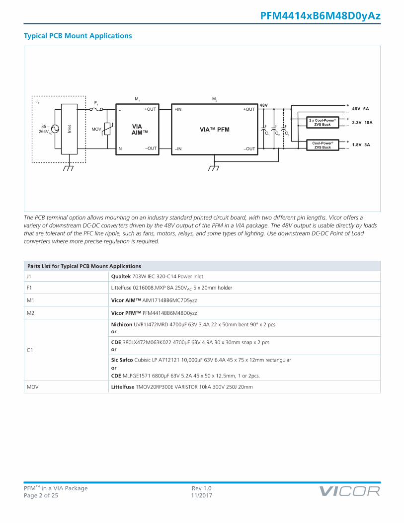
Typical PCB Mount Applications
The PCB terminal option allows mounting on an industry standard printed circuit board, with two different pin lengths. Vicor offers a variety of downstream DC-DC converters driven by the 48V output of the PFM in a VIA package. The 48V output is usable directly by loads that are tolerant of the PFC line ripple, such as fans, motors, relays, and some types of lighting. Use downstream DC-DC Point of Load converters where more precise regulation is required.
Parts List for Typical PCB Mount Applications
J1 Qualtek 703W IEC 320-C14 Power Inlet
F1 Littelfuse 0216008.MXP 8A 250VAC 5 x 20mm holder
M1 Vicor AIM™ AIM1714BB6MC7D5yzz
M2 Vicor PFM™ PFM4414BB6M48D0yzz
C1
Nichicon UVR1J472MRD 4700µF 63V 3.4A 22 x 50mm bent 90° x 2 pcsor
CDE 380LX472M063K022 4700µF 63V 4.9A 30 x 30mm snap x 2 pcs or
Sic Safco Cubisic LP A712121 10,000µF 63V 6.4A 45 x 75 x 12mm rectangular
or
CDE MLPGE1571 6800µF 63V 5.2A 45 x 50 x 12.5mm, 1 or 2pcs.
MOV Littelfuse TMOV20RP300E VARISTOR 10kA 300V 250J 20mm

PFM™ in a VIA Package Rev 1.0Page 3 of 25 11/2017
PFM4414xB6M48D0yAz
VIA™ PFM
+IN
–IN
+OUT
–OUT
Fan
Relays
Coin BoxControllerDispensors
48V
16
8
8
J1
85 – 264VAC In
let
M1
AIM™VIA
F1
M2
+OUT
–OUT
L
N
MOV +
C1
+
C2
+
C3
Typical Chassis Mount Applications
The PFM in a VIA package is available in Chassis Mount option, saving the cost of a PCB and allowing access to both sides of the power supply for cooling. The parts list below minimizes the number of interconnects required between necessary components, and selects components with terminals traditionally used for point to point chassis wiring.
Parts List for Typical Chassis Mount Applications
J1 Qualtek 719W or 723W IEC 320-C14 Power Inlet
F1 Littelfuse 0216008.MXP 8A 250VAC 5 x 20mm in a J1, or separate fuse holder
M1 Vicor AIM™ AIM1714VB6MC7D5y00
M2 Vicor PFM™ PFM4414VB6M48D0y00
C1
UCC E32D630HPN103MA67M 10,000µF, 63V 7.4A, 35 x 67mm screw terminal
or
Kemet ALS30A103DE063, 10,000µF 63V 10.8A 36 x 84mm screw terminal
MOV Littelfuse TMOV20RP300E VARISTOR 10kA 300V 250 20mm

PFM™ in a VIA Package Rev 1.0Page 4 of 25 11/2017
PFM4414xB6M48D0yAz
1
2 4
+IN +OUT
TOP VIEW
4414 VIA™ PFM - Chassis Mount - Terminals Up
3
–OUT–IN
2
1 3
–IN –OUT
TOP VIEW
4414 VIA PFM - PCB Mount - Pins Down
4
+OUT+IN
Pin Configuration
Pin Descriptions
Please note that these Pin drawings are not to scale.
Pin Number Signal Name Type Function
1 +IN INPUT POWER Positive input power terminal
2 –ININPUT POWER
RETURNNegative input power terminal
3 +OUT OUTPUT POWER Positive output power terminal
4 –OUTOUTPUT POWER
RETURNNegative output power terminal

PFM™ in a VIA Package Rev 1.0Page 5 of 25 11/2017
PFM4414xB6M48D0yAz
Out
put C
urre
nt (A
)
Case Temperature (°C)Current Power
0
100
200
300
400
500
0.00
2.00
4.00
6.00
8.00
10.00
-60 -40 -20 0 20 40 60 80 100
Out
put P
ower
(W)
Safe Operating Area
Absolute Maximum Ratings
The absolute maximum ratings below are stress ratings only. Operation at or beyond these maximum ratings can cause permanent damage to the device.
Parameter Comments Min Max Unit
Input Voltage +IN to –IN 1ms max 0 600 VPK
Input Voltage (+IN to –IN) Continuous, Rectified 0 275 VRMS
Output Voltage (+OUT to –OUT) –0.5 58 VDC
Output Current 0.0 12.4 A
Screw Torque 4 mounting, 2 input, 2 output 4 [0.45] in.lbs [N.m]
Operating Junction Temperature T-Grade –40 125 °C
Storage Temperature T-Grade –65 125 °C
Dielectric Withstand * See note below
Input – Case Basic Insulation 2121 VDC
Input – OutputReinforced Insulation (Internal ChiP™ tested at 4242VDC prior to assembly.)
2121 VDC
Output – Case Functional Insulation 707 VDC
* Please see Dielectric Withstand section. See page 19.
PFM™ in a VIA Package Rev 1.0Page 6 of 25 11/2017
PFM4414xB6M48D0yAz
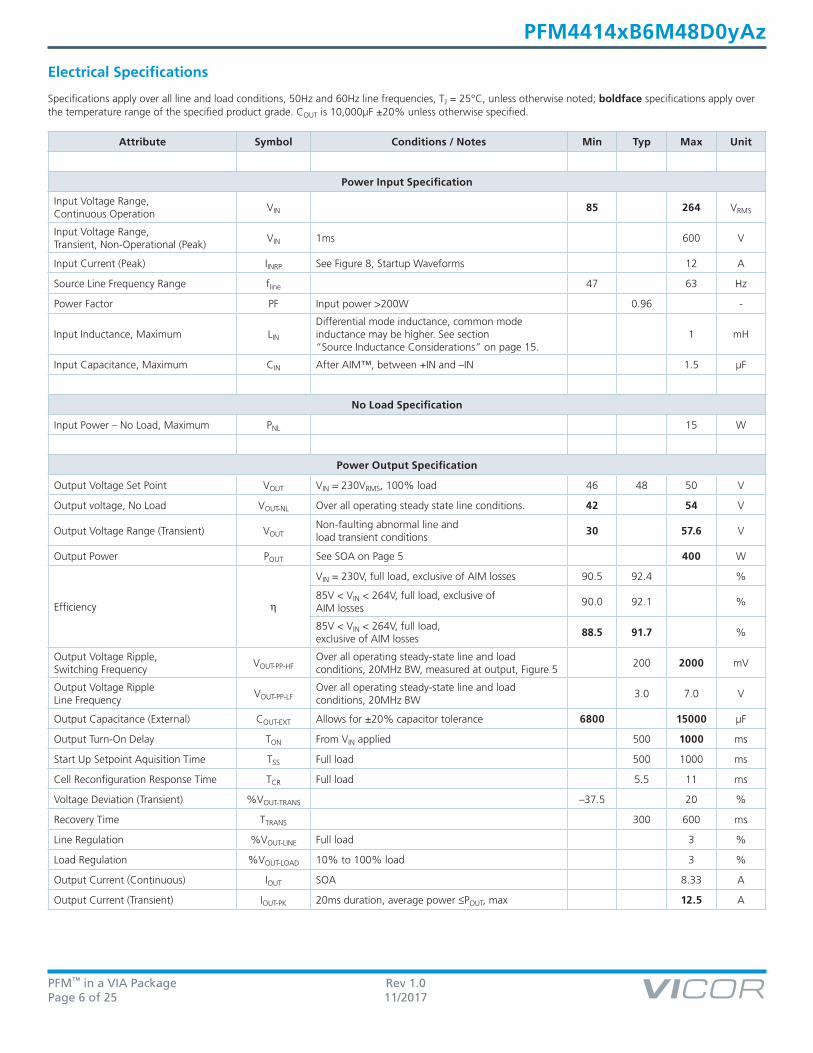
Electrical Specifications
Specifications apply over all line and load conditions, 50Hz and 60Hz line frequencies, TJ = 25°C, unless otherwise noted; boldface specifications apply over the temperature range of the specified product grade. COUT is 10,000µF ±20% unless otherwise specified.
Attribute Symbol Conditions / Notes Min Typ Max Unit
Power Input Specification
Input Voltage Range, Continuous Operation
VIN 85 264 VRMS
Input Voltage Range, Transient, Non-Operational (Peak)
VIN 1ms 600 V
Input Current (Peak) IINRP See Figure 8, Startup Waveforms 12 A
Source Line Frequency Range fline 47 63 Hz
Power Factor PF Input power >200W 0.96 -
Input Inductance, Maximum LIN
Differential mode inductance, common mode inductance may be higher. See section “Source Inductance Considerations” on page 15.
1 mH
Input Capacitance, Maximum CIN After AIM™, between +IN and –IN 1.5 µF
No Load Specification
Input Power – No Load, Maximum PNL 15 W
Power Output Specification
Output Voltage Set Point VOUT VIN = 230VRMS, 100% load 46 48 50 V
Output voltage, No Load VOUT-NL Over all operating steady state line conditions. 42 54 V
Output Voltage Range (Transient) VOUTNon-faulting abnormal line and load transient conditions
30 57.6 V
Output Power POUT See SOA on Page 5 400 W
Efficiency η
VIN = 230V, full load, exclusive of AIM losses 90.5 92.4 %
85V < VIN < 264V, full load, exclusive of AIM losses
90.0 92.1 %
85V < VIN < 264V, full load,exclusive of AIM losses
88.5 91.7 %
Output Voltage Ripple,Switching Frequency
VOUT-PP-HFOver all operating steady-state line and load conditions, 20MHz BW, measured at output, Figure 5
200 2000 mV
Output Voltage RippleLine Frequency
VOUT-PP-LFOver all operating steady-state line and load conditions, 20MHz BW
3.0 7.0 V
Output Capacitance (External) COUT-EXT Allows for ±20% capacitor tolerance 6800 15000 µF
Output Turn-On Delay TON From VIN applied 500 1000 ms
Start Up Setpoint Aquisition Time TSS Full load 500 1000 ms
Cell Reconfiguration Response Time TCR Full load 5.5 11 ms
Voltage Deviation (Transient) %VOUT-TRANS –37.5 20 %
Recovery Time TTRANS 300 600 ms
Line Regulation %VOUT-LINE Full load 3 %
Load Regulation %VOUT-LOAD 10% to 100% load 3 %
Output Current (Continuous) IOUT SOA 8.33 A
Output Current (Transient) IOUT-PK 20ms duration, average power ≤POUT, max 12.5 A
PFM™ in a VIA Package Rev 1.0Page 7 of 25 11/2017
PFM4414xB6M48D0yAz
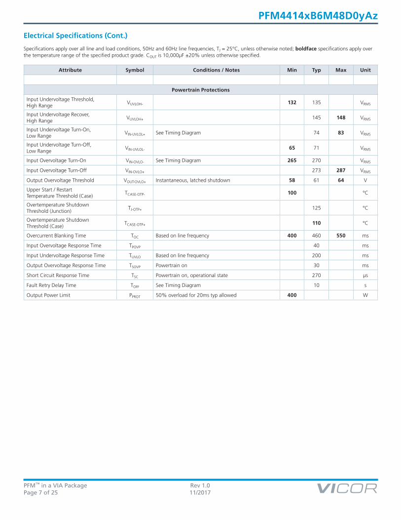
Electrical Specifications (Cont.)
Specifications apply over all line and load conditions, 50Hz and 60Hz line frequencies, TJ = 25°C, unless otherwise noted; boldface specifications apply over the temperature range of the specified product grade. COUT is 10,000µF ±20% unless otherwise specified.
Attribute Symbol Conditions / Notes Min Typ Max Unit
Powertrain Protections
Input Undervoltage Threshold, High Range
VUVLOH- 132 135 VRMS
Input Undervoltage Recover, High Range
VUVLOH+ 145 148 VRMS
Input Undervoltage Turn-On, Low Range
VIN-UVLOL+ See Timing Diagram 74 83 VRMS
Input Undervoltage Turn-Off, Low Range
VIN-UVLOL- 65 71 VRMS
Input Overvoltage Turn-On VIN-OVLO- See Timing Diagram 265 270 VRMS
Input Overvoltage Turn-Off VIN-OVLO+ 273 287 VRMS
Output Overvoltage Threshold VOUT-OVLO+ Instantaneous, latched shutdown 58 61 64 V
Upper Start / Restart Temperature Threshold (Case)
TCASE-OTP- 100 °C
Overtemperature ShutdownThreshold (Junction)
TJ-OTP+ 125 °C
Overtemperature Shutdown Threshold (Case)
TCASE-OTP+ 110 °C
Overcurrent Blanking Time TOC Based on line frequency 400 460 550 ms
Input Overvoltage Response Time TPOVP 40 ms
Input Undervoltage Response Time TUVLO Based on line frequency 200 ms
Output Overvoltage Response Time TSOVP Powertrain on 30 ms
Short Circuit Response Time TSC Powertrain on, operational state 270 µs
Fault Retry Delay Time TOFF See Timing Diagram 10 s
Output Power Limit PPROT 50% overload for 20ms typ allowed 400 W
PFM™ in a VIA Package Rev 1.0Page 8 of 25 11/2017
PFM4414xB6M48D0yAz
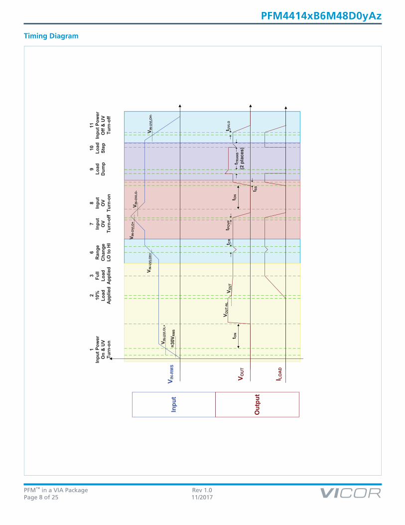
Timing Diagram
V IN
-RM
S
V OU
T
I LOA
D
V IN
-OVL
O+
1In
put P
ower
O
n &
UV
Turn
-on
3 Full
Load
A
pplie
d
6R
ange
Cha
nge
LO to
HI
7In
put
OV
Turn
-off
8In
put
OV
Turn
-on
9Lo
adD
ump
10 Load
St
ep
11In
put P
ower
O
ff &
UV
Turn
-off
Inpu
t
Out
put
t CR
t ON
V IN
-UVL
OL+
≈30V
RM
S
210
%Lo
ad
App
lied
t TR
AN
S (2
pla
ces)
V IN
-OVL
O-
V IN
-UVL
OH
-V I
N-U
VLO
H+
V OU
T-N
LV O
UT
t ON
t PO
VPt U
VLO
t SS

PFM™ in a VIA Package Rev 1.0Page 9 of 25 11/2017
PFM4414xB6M48D0yAz
Timing Diagram (Cont.)
V IN
-RM
S
V OU
T
I LOA
D
t ON
V
t OC
t OFF
+tO
Nt O
FF+t
ON
t OC
≥tO
FF+t
ON
V OU
T-O
VLO
+
t SO
VPt S
S
V IN
-UVL
OL-
t SC
t OFF
+tO
N
t OFF
+tO
N
t OC
)) ))
13In
put P
ower
O
N &
UV
Turn
-on
14O
utpu
t OC
Fa
ult
15O
utpu
t O
C
Rec
over
y
18O
utpu
t O
VPFa
ult
19R
ecyc
le
Inpu
t Po
wer
(O
utpu
t O
VP
Rec
over
y)
20O
utpu
t SC Fa
ult
21O
utpu
tSC
R
ecov
ery
22O
T Fa
ult
&R
ecov
ery
23 Line
D
rop-
Out
24 Inpu
t Po
wer
O
ff &
UV
Turn
-off
Inpu
t
Out
put
t ON
V IN
-UVL
OL+
)) ))
*
IN-U
VLO
L+

PFM™ in a VIA Package Rev 1.0Page 10 of 25 11/2017
PFM4414xB6M48D0yAz
Application CharacteristicsEf
ficie
ncy
(%)
Input Line Voltage
90.0
90.5
91.0
91.5
92.0
92.5
93.0
93.5
85 105 125 145 165 185 205 225 245 265
25°C –40°C 80°C
Figure 1 — Full load efficiency vs. line voltage
No
Load
Pow
er D
issi
patio
n (W
)
Input Line Voltage
2
4
6
8
10
12
85 105 125 145 165 185 205 225 245 265
25°C -40°C 80°C
Figure 2 — Typical no load power dissipation vs. VIN , module enabled
Cur
rent
(mA
)
230V, 50Hz 1/3x EN61000-3-2, Class A EN61000-3-2, Class D
0
100
200
300
400
500
600
700
800
1 3 5 7 9 11 13 15 17 19 21 23 25 27 29 31 33 35 37 39
Figure 3 — Typical input current harmonics, full load vs. VIN using typical applications circuit on pages 2 & 3
Figure 5 — Typical switching frequency output voltage ripple waveform, TCASE = 30ºC, VIN = 230V, IOUT = 8.3A, no external ceramic capacitance, 20MHz BW
Pow
er F
acto
r
Output Power (W)120V/60Hz 230V/50Hz 100V/50HzVIN:
0.80 0.82 0.84 0.86 0.88 0.90 0.92 0.94 0.96 0.98 1.00
0 100 200 300 400
Figure 4 — Typical power factor vs. VIN and IOUT using typical applications circuit on pages 2 & 3
Figure 6 — Typical line frequency output voltage ripple waveform, TCASE = 30ºC, VIN = 230V, IOUT = 8.3A, COUT = 10,000µF. 20MHz BW
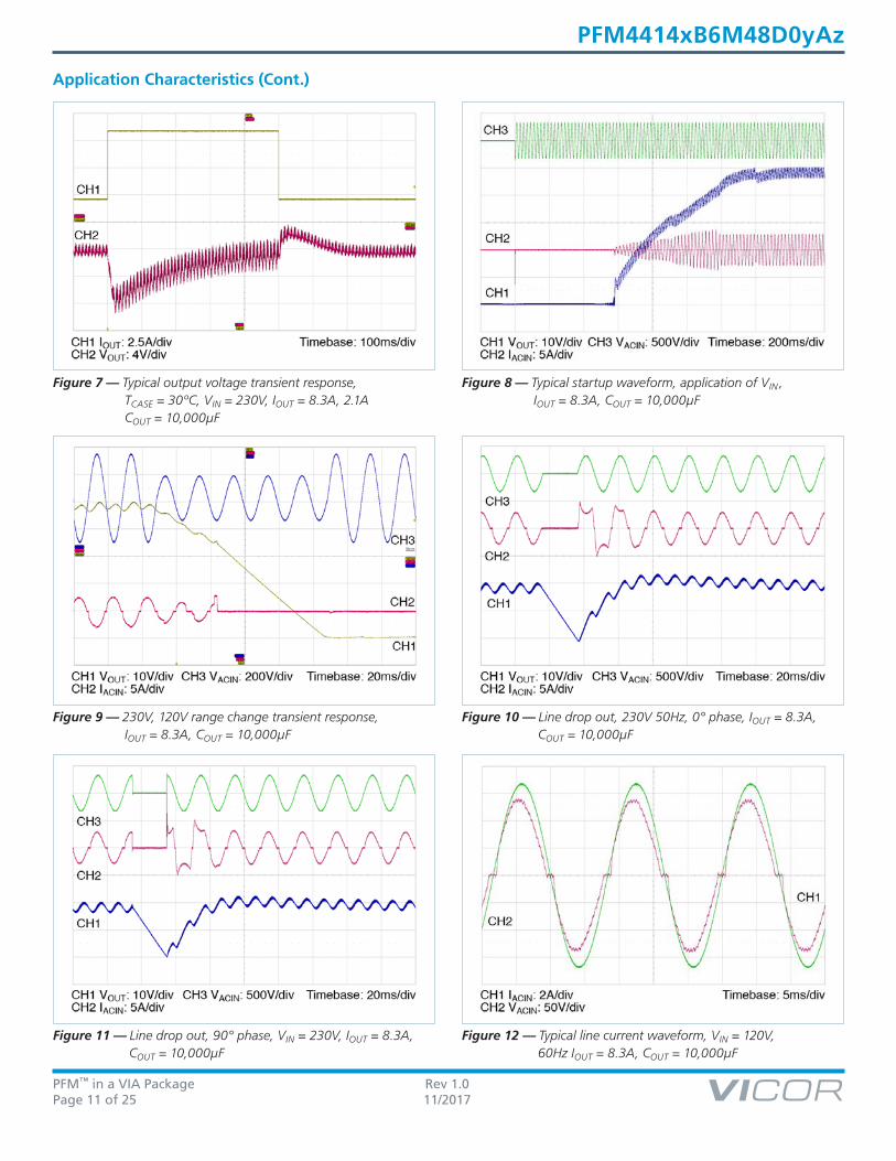
PFM™ in a VIA Package Rev 1.0Page 11 of 25 11/2017
PFM4414xB6M48D0yAz
Figure 12 — Typical line current waveform, VIN = 120V, 60Hz IOUT = 8.3A, COUT = 10,000µF
Figure 11 — Line drop out, 90° phase, VIN = 230V, IOUT = 8.3A, COUT = 10,000µF
Figure 10 — Line drop out, 230V 50Hz, 0° phase, IOUT = 8.3A, COUT = 10,000µF
Figure 9 — 230V, 120V range change transient response, IOUT = 8.3A, COUT = 10,000µF
Figure 7 — Typical output voltage transient response, TCASE = 30ºC, VIN = 230V, IOUT = 8.3A, 2.1A COUT = 10,000µF
Figure 8 — Typical startup waveform, application of VIN , IOUT = 8.3A, COUT = 10,000µF
Application Characteristics (Cont.)
PFM™ in a VIA Package Rev 1.0Page 12 of 25 11/2017
PFM4414xB6M48D0yAz
Load Current (A)
Effic
ienc
y (%
)
Pow
er D
issi
patio
n (W
)
85V 115V 230V
V :IN 85V 115V 230V Eff
P Diss
10
15
20
25
30
35
40
45
50
78
80
82
84
86
88
90
92
94
0 1 2 3 4 5 6 7 8 9
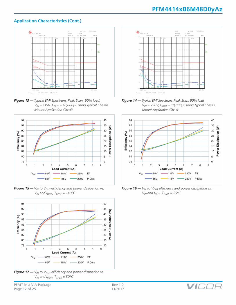
Figure 17 — VIN to VOUT efficiency and power dissipation vs. VIN and IOUT , TCASE = 80ºC
150 kHz 30 MHz
Trd 55022RED
SGL
2AV
Unit dB V
1QP
ResBW 9 kHzMeas T 20 ms
Det QPAtt 20 dB
INPUT 2
13.Jul 2017 14:25
1 MHz 10 MHz
30
40
50
60
70
80
90
20
100
22QPB
22AVB
Date: 13.JUL.2017 14:25:07
Figure 13 — Typical EMI Spectrum, Peak Scan, 90% load, VIN = 115V, COUT = 10,000µF using Typical Chassis Mount Application Circuit
Application Characteristics (Cont.)
150 kHz 30 MHz
Trd 55022RED
SGL
2AV
Unit dB V
1QP
ResBW 9 kHzMeas T 20 ms
Det QPAtt 20 dB
INPUT 2
13.Jul 2017 12:29
1 MHz 10 MHz
30
40
50
60
70
80
90
20
100
22QPB
22AVB
Date: 13.JUL.2017 12:29:36
Figure 14 — Typical EMI Spectrum, Peak Scan, 90% load, VIN = 230V, COUT = 10,000µF using Typical Chassis Mount Application Circuit
Load Current (A)
Effic
ienc
y (%
)
Pow
er D
issi
patio
n (W
)
85V 115V 230V
V :IN 85V 115V 230V Eff
P Diss
0
5
10
15
20
25
30
35
40
78
80
82
84
86
88
90
92
94
0 1 2 3 4 5 6 7 8 9
Figure 15 — VIN to VOUT efficiency and power dissipation vs. VIN and IOUT , TCASE = –40ºC
Load Current (A)
Effic
ienc
y (%
)
Pow
er D
issi
patio
n (W
)
85V 115V 230V
V :IN 85V 115V 230V Eff
P Diss
0
5
10
15
20
25
30
35
40
78
80
82
84
86
88
90
92
94
0 1 2 3 4 5 6 7 8 9
Figure 16 — VIN to VOUT efficiency and power dissipation vs. VIN and IOUT , TCASE = 25ºC

PFM™ in a VIA Package Rev 1.0Page 13 of 25 11/2017
PFM4414xB6M48D0yAz
General Characteristics
Specifications apply over all line and load conditions, 50Hz and 60Hz line frequencies, TC = 25°C, unless otherwise noted; boldface specifications apply over the temperature range of the specified Product Grade.
Attribute Symbol Conditions / Notes Min Typ Max Unit
Mechanical
Length L 110.6 [4.35] mm [in]
Width W 35.5 [1.40] mm [in]
Height H 9.3 [0.37] mm [in]
Volume Vol Without heatsink 36.9 [2.25] cm3 [in3]
Weight W 148 [5.2] g [oz]
Pin Material C145 copper, half hard
Underplate Low stress ductile nickel 50 100 µin
Pin FinishPalladium 0.8 6 µin
Soft Gold 0.12 2 µin
Thermal
Operating Case Temperature TC
C-Grade, see derating curve in SOA –20 100 °C
T-Grade, see derating curve in SOA –40 100 °C
Thermal Resistance, Junction to Case, Top
RJC_TOP 1.34 °C/W
Thermal Resistance, Junction to Case, Bottom
RJC_BOT 1.72 °C/W
Coupling Thermal Resistance,Top to Bottom of Case, Internal
RHOU 0.57 °C/W
Shell Thermal Capacity 54 J/K
Thermal Design See Thermal Considerations on Page 17
Assembly
ESD Rating
ESDHBMHuman Body Model, JEDEC JESD 22-A114C.01
1,000
VESDMMMachine Model,JEDEC JESD 22-A115B
N/A
ESDCDMCharged Device Model,JEDEC JESD 22-C101D
200
Safety
Agency Approvals / Standards
cTUVus, EN60950-1 and IEC 60950-1
cURus, UL 60950-1 and CAN/CSA 60950-1
CE Marked for Low Voltage Directive and RoHS Recast Directive, as applicable
Touch Current measured in accordance with IEC 60990 using measuring network Figure 3 (PFM in a VIA™ package only)
0.5 mA
PFM™ in a VIA Package Rev 1.0Page 14 of 25 11/2017
PFM4414xB6M48D0yAz
General Characteristics (Cont.)
Specifications apply over all line and load conditions, 50Hz and 60Hz line frequencies, TC = 25°C, unless otherwise noted; boldface specifications apply over the temperature range of the specified Product Grade.
Attribute Symbol Conditions / Notes Min Typ Max Unit
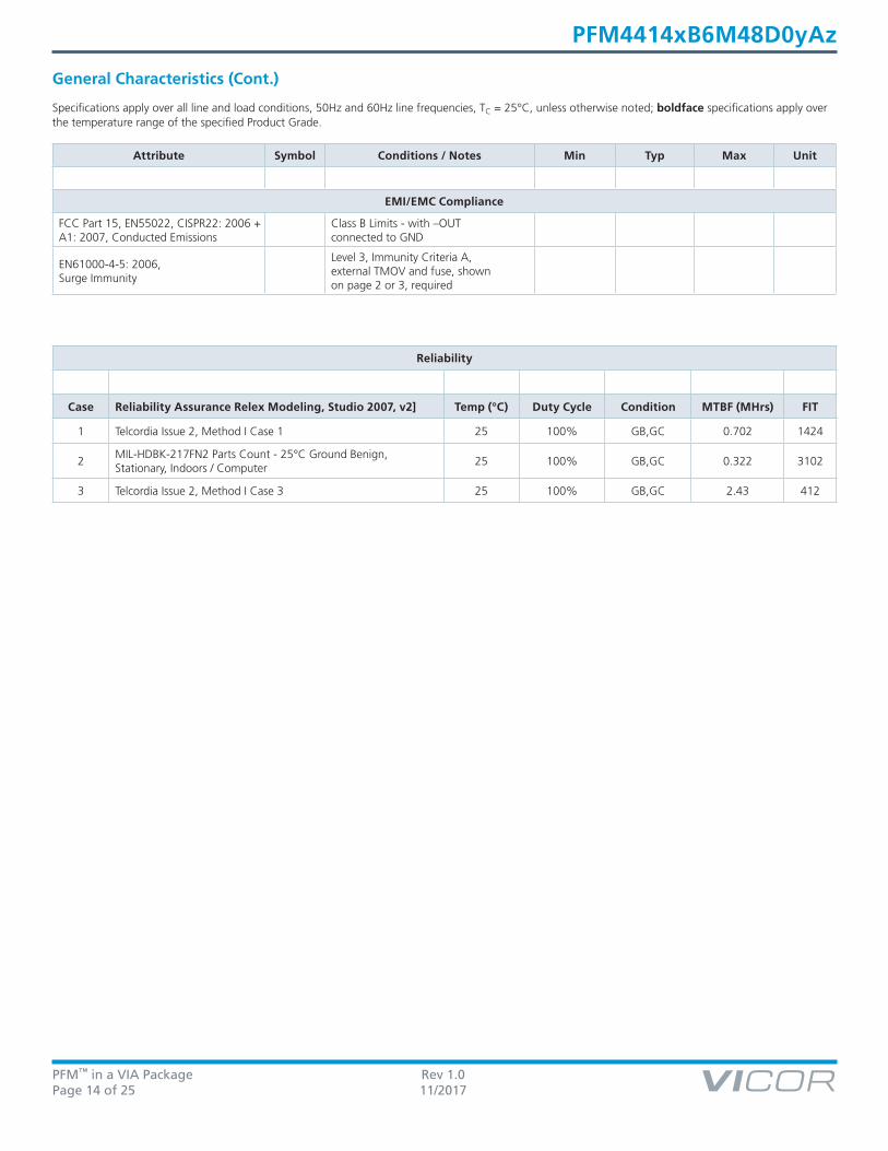
EMI/EMC Compliance
FCC Part 15, EN55022, CISPR22: 2006 + A1: 2007, Conducted Emissions
Class B Limits - with –OUTconnected to GND
EN61000-4-5: 2006, Surge Immunity
Level 3, Immunity Criteria A,external TMOV and fuse, shown on page 2 or 3, required
Reliability
Case Reliability Assurance Relex Modeling, Studio 2007, v2] Temp (°C) Duty Cycle Condition MTBF (MHrs) FIT
1 Telcordia Issue 2, Method I Case 1 25 100% GB,GC 0.702 1424
2MIL-HDBK-217FN2 Parts Count - 25°C Ground Benign, Stationary, Indoors / Computer
25 100% GB,GC 0.322 3102
3 Telcordia Issue 2, Method I Case 3 25 100% GB,GC 2.43 412

PFM™ in a VIA Package Rev 1.0Page 15 of 25 11/2017
PFM4414xB6M48D0yAz
Product Details and Design Guidelines
Building Blocks and System Designs
The PFM in a VIA™ package is a high efficiency AC-DC converter, operating from a universal AC input to generate an isolated SELV 48VDC output bus with power factor correction. It is the key component of an AC-DC power supply system such as the one shown in Figure 18 above.
The input to the PFM in a VIA package is a rectified sinusoidal AC source with a power factor maintained by the module with harmonics conforming to IEC 61000-3-2. Internal filtering enables compliance with the standards relevant to the application (Surge, EMI, etc.). See EMI/EMC Compliance standards on Page 14.
The module uses secondary-side energy storage (at the SELV 48V bus) to maintain output hold up through line dropouts and brownouts. Downstream regulators also provide tighter voltage regulation, if required.
Traditional PFC Topology
To cope with input voltages across worldwide AC mains (85 – 264VAC), traditional AC-DC power supplies (Figure 19) use two power conversion stages: 1) a PFC boost stage to step up from a rectified input as low as 85VAC to ~380VDC; and 2) a DC-DC down converter from 380VDC to a 48V bus.
The efficiency of the boost stage and of traditional power supplies is significantly compromised operating from worldwide AC lines as low as 85VAC.
Adaptive Cell™ Topology
With its single stage Adaptive Cell™ topology, the PFM in a VIA package enables consistently high efficiency conversion from worldwide AC mains to a 48V bus and efficient secondary-side power distribution.
Input Fuse Selection
PFM in a VIA package products are not internally fused in order to provide flexibility in configuring power systems. Input line fusing is recommended at system level, in order to provide thermal protection in case of catastrophic failure. The fuse shall be selected by closely matching system requirements with the following characteristics:
nn Recommended fuse: 216 Series Littelfuse 8A or lower current rating (usually greater than the PFM maximum current at lowest input voltage)
nn Maximum voltage rating (usually greater than the maximum possible input voltage)
nn Ambient temperature
nn Breaking capacity per application requirements
nn Nominal melting I2t
Source Inductance Considerations
The PFM Powertrain uses a unique Adaptive Cell Topology that dynamically matches the powertrain architecture to the AC line voltage. In addition the PFM uses a unique control algorithm to reduce the AC line harmonics yet still achieve rapid response to dynamic load conditions presented to it at the DC output terminals. Given these unique power processing features, the PFM can expose deficiencies in the AC line source impedance that may result in unstable operation if ignored.
It is recommended that for a single PFM, the line source inductance should be no greater than 1mH for a universal AC input of 100 – 240V. If the PFM will be operated at 240V nominal only, the source impedance may be increased to 2mH. For either of the preceding operating conditions it is best to be conservative and stay below the maximum source inductance values. When multiple PFM’s are used on a single AC line, the inductance should be no greater than 1mH/N, where N is the number of PFM’s on the AC branch circuit, or 2mH/N for 240VAC operation. It is important to consider all potential sources of series inductance including and not limited to, AC power distribution transformers, structure wiring inductance, AC line reactors, and additional line filters. Non-linear behavior of power distribution devices ahead of the PFM may further reduce the maximum inductance and require testing to ensure optimal performance.
If the PFM is to be utilized in large arrays, the PFMs should be spread across multiple phases or sources thereby minimizing the source inductance requirements, or be operated at a line voltage close to 240VAC. Vicor Applications should be contacted to assist in the review of the application when multiple devices are to be used in arrays.
Figure 18 — 400W Universal AC-DC Supply
Full WaveRectifier
EMI/TVSFilter
IsolatedDC / DC
Converter48V Bus
Figure 19 — Traditional PFC AC-DC supply
+IN
-IN
+OUT
-OUTHoldup Capacitor
PFM™VIA
AIM™VIA
+OUT
-OUT
L
N

PFM™ in a VIA Package Rev 1.0Page 16 of 25 11/2017
PFM4414xB6M48D0yAz
Fault Handling
Input Undervoltage (UV) Fault ProtectionThe input voltage is monitored by the microcontroller to detect an input under voltage condition. When the input voltage is less than the UVLO threshold, a fault is detected. After a time tUVLO, the unit shuts down. Faults lasting less than tUVLO may not be detected. Such a fault does not go through an auto-restart cycle. Once the input voltage rises above the UVLO threshold, the unit recovers from the input UV fault, the powertrain resumes normal switching after a time tON and the output voltage of the unit reaches the set point voltage within a time tSS.
Overcurrent (OC) Fault ProtectionAs long as the fault persists, the module goes through an auto-restart cycle with off time equal to tOFF + tON and on time equal to tOC. Faults shorter than a time tOC may not be detected. Once the fault is cleared, the module follows its normal start up sequence after a time tOFF.
Short Circuit (SC) Fault ProtectionThe module responds to a short circuit event within a time tSC. The module then goes through an auto restart cycle, with an off time equal to tOFF + tON and an on time equal to tSC, for as long as the short circuit fault condition persists. Once the fault is cleared, the unit follows its normal start up sequence after a time tOFF. Faults shorter than a time tSC may not be detected.
Temperature Fault ProtectionThe microcontroller monitors the temperature within the PFM. If this temperature exceeds TJ-OTP+, an overtemperature fault is detected, and the output voltage of the PFM falls. Once the case temperature falls below TCASE-OTP-, after a time greater than or equal to tOFF, the converter recovers and undergoes a normal restart. For the C-grade version of the converter, this temperature is 75°C. Faults shorter than a time tOTP may not be detected. If the temperature falls below TCASE-UTP-, an undertemperature fault is detected, and the output voltage of the unit falls. Once the case temperature rises above TCASE-UTP, after a time greater than or equal to tOFF, the unit recovers and undergoes a normal restart.
Output Overvoltage Protection (OVP)The microcontroller monitors the primary sensed output voltage to detect output OVP. If the primary sensed output voltage exceeds VOUT-OVLO+, a fault is latched, and the output voltage of the module falls after a time tSOVP. Faults shorter than a time tSOVP may not be detected. This type of fault is a latched fault and requires that the input power be recycled to recover from the fault.
Ruggedized Auto Range Functionality
The input voltage range is determined at power up time, to cover the input voltage range of either 85 – 132VRMS or 170 – 264VRMS, called low range and high range. Once selected, dynamic range changes are limited by the logic explained below.
In low range, operation continues until the input either drops under the UVLO threshold (in which case the converter turns off), or until the input exceeds the range transition threshold.
The increase in input voltage can be temporary, as when handling a surge on the input, or it could be permanent, as can happen in the rare occasion when an input is turned on during a brown-out or sag condition on a high voltage system:
nn If the increase is temporary, and the input returns under range transition threshold within 0.8s, operation continues in low range.
nn If the input stays over the range transition threshold, the converter changes to high range.
In high range, operation continue up to to the OVLO. A surge will cause the power train to turn off on a short term basis to protect itself during the rise in input voltage, and it will return to operation when the input returns to the operating range.
When the input crosses under the range transition threshold, the input turns off as it considers this to be the high range UVLO threshold. If the converter returns above the range transition threshold within 50ms, the converter will resume operation in high range. If the converter does not return to operating range, the system will reset to the default power down condition, monitoring the input and waiting to decide whether it should startup into low range or high range.
PFM™ in a VIA Package Rev 1.0Page 17 of 25 11/2017
PFM4414xB6M48D0yAz
Input Line Cycle Skipping
This model does not have input line cycle skipping. As a result, the regulation spec is guaranteed from no load to full load. Because of this, this model does not present high peak to peak output voltage under low load conditions, limiting perturbation that may affect downstream regulators ability to regulate their outputs as tightly as desired. The only sources of output voltage perturbation (from largest to smallest amplitude) are:
nn Discharge of output bulk caps during a dropout condition
nn Surge transients that can cause similar dropout or short term range change
nn Input line cycle ripple, with amplitude proportional to output current
nn Switching frequency ripple, which can be reduced further with a higher frequency filter stage if necessary
Noise sensitive applications should still test to ensure they can handle or safely ignore these AC transitions on the PFM output bus, which are expected to be handled by the downstream point of load regulators.
Hold-Up Capacitance
The PFM in a VIA™ package uses secondary-side energy storage (at the SELV 48V bus) and downstream regulators to maintain output hold up through line dropouts and brownouts. The module’s output bulk capacitance can be sized to achieve the required hold up functionality.
Hold-up time depends upon the output power drawn from the PFM in a VIA package based AC-DC front end and the input voltage range of downstream DC-DC converters.
The following formula can be used to calculate hold-up capacitance for a system comprised of PFM and a downstream regulator:
Where:
C VIA PFM’s output bulk capacitance in Farads
td Hold-up time in seconds
POUT VIA PFM’s output power in Watts
V2 Output voltage of VIA PFM’s converter in Volts
V1 Downstream regulator undervoltage turn off (Volts) –OR– POUT / IOUT-PK, whichever is greater.
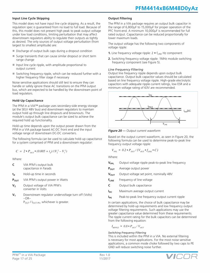
Output Filtering
The PFM in a VIA package requires an output bulk capacitor in the range of 6,800µF to 15,000µF for proper operation of the PFC front-end. A minimum 10,000µF is recommended for full rated output. Capacitance can be reduced proportionally for lower maximum loads.
The output voltage has the following two components of voltage ripple:
1. Line frequency voltage ripple: 2 • fLINE Hz component
2. Switching frequency voltage ripple: 1MHz module switching frequency component (see Figure 5).
Line Frequency FilteringOutput line frequency ripple depends upon output bulk capacitance. Output bulk capacitor values should be calculated based on line frequency voltage ripple. High-grade electrolytic capacitors with adequate ripple current ratings, low ESR and a minimum voltage rating of 63V are recommended.
Based on the output current waveform, as seen in Figure 20, the following formula can be used to determine peak-to-peak line frequency output voltage ripple:
Where:
VPPL Output voltage ripple peak-to-peak line frequency
POUT Average output power
VOUT Output voltage set point, nominally 48V
fLINE Frequency of line voltage
C Output bulk capacitance
IDC Maximum average output current
IPK Peak-to-peak line frequency output current ripple
In certain applications, the choice of bulk capacitance may be determined by hold-up requirements and low frequency output voltage filtering requirements. Such applications may use the greater capacitance value determined from these requirements. The ripple current rating for the bulk capacitors can be determined from the following equation:
Switching Frequency FilteringThis is included within the PFM in a VIA. No external filtering is necessary for most applications. For the most noise sensitive applications, a common mode choke followed by two caps to PE GND will reduce switching noise further.
lPK
lPK/2
loutDC
lfLINE
Figure 20 — Output current waveform
C = 2 • POUT • (0.005 + td) / (V22 – V1
2) VPPL ~ 0.2 • POUT / (VOUT • fLINE • C)~
IRIPPLE ~ 0.8 • POUT / VOUT~
PFM™ in a VIA Package Rev 1.0Page 18 of 25 11/2017
PFM4414xB6M48D0yAz
EMI Filtering and Transient Voltage Suppression
EMI FilteringThe PFM with PFC is designed such that it will comply with EN55022 Class B for Conducted Emissions with the Vicor AIM™, AIM1714xB6MC7D5yzz. The emissions spectrum is shown in Figures 13 & 14. If the positive output is connected to earth ground or both output terminals are to be left floating, a 4700pF 500V capacitor on the –OUT terminal to ground is also recommended.
EMI performance is subject to a wide variety of external influences such as PCB construction, circuit layout etc. As such, external components in addition to those listed herein may be required in specific instances to gain full compliance to the standards specified. Radiated emissions require certification at the system level. For best results, enclose the product in a steel enclosure. Filtering must be considered for every conductor leaving the enclosure, which can present itself as a potential transmission antenna.
Transient Voltage SuppressionThe PFM contains line transient suppression circuitry to meet specifications for surge (i.e. EN61000-4-5) and fast transient conditions (i.e. EN61000-4-4 fast transient/“burst”) when coupled with an external TMOV as shown on pages 2 and 3.
When more than one PFM is used in a system, each PFM should have its own fuse, TMOV and VIA™ AIM.
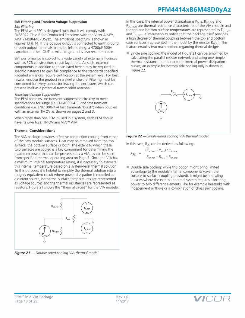
Thermal Considerations
The VIA package provides effective conduction cooling from either of the two module surfaces. Heat may be removed from the top surface, the bottom surface or both. The extent to which these two surfaces are cooled is a key component for determining the maximum power that can be processed by a VIA, as can be seen from specified thermal operating area on Page 5. Since the VIA has a maximum internal temperature rating, it is necessary to estimate this internal temperature based on a system-level thermal solution. To this purpose, it is helpful to simplify the thermal solution into a roughly equivalent circuit where power dissipation is modeled as a current source, isothermal surface temperatures are represented as voltage sources and the thermal resistances are represented as resistors. Figure 21 shows the “thermal circuit” for the VIA module.
In this case, the internal power dissipation is PDISS, RJC_TOP and RJC_BOT are thermal resistance characteristics of the VIA module and the top and bottom surface temperatures are represented as TC_TOP, and TC_BOT. It interesting to notice that the package itself provides a high degree of thermal coupling between the top and bottom case surfaces (represented in the model by the resistor RHOU). This feature enables two main options regarding thermal designs:
nn Single side cooling: the model of Figure 21 can be simplified by calculating the parallel resistor network and using one simple thermal resistance number and the internal power dissipation curves; an example for bottom side cooling only is shown in Figure 22.
In this case, RJC can be derived as following:
nn Double side cooling: while this option might bring limited advantage to the module internal components (given the surface-to-surface coupling provided), it might be appealing in cases where the external thermal system requires allocating power to two different elements, like for example heatsinks with independent airflows or a combination of chassis/air cooling.
PDISS
+
–
TC_TOP
–
TC_BOT
RJC_TOP
RJC_BOT
RHOU
s
s
+
Figure 21 — Double sided cooling VIA thermal model
PDISS
+ –TC_BOT
RJC
s
s
Figure 22 — Single-sided cooling VIA thermal model
(RJC_TOP + RHOU) • RJC_BOTRJC =
RJC_TOP + RHOU + RJC_BOT

PFM™ in a VIA Package Rev 1.0Page 19 of 25 11/2017
PFM4414xB6M48D0yAz
Powering a Constant Power Load
When the output voltage of the PFM in a VIA™ package module is applied to the input of the downstream regulator, the regulator turns on and acts as a constant-power load. When the module’s output voltage reaches the input undervoltage turn on of the regulator, the regulator will attempt to start. However, the current demand of the downstream regulator at the undervoltage turn-on point and the hold-up capacitor charging current may force the PFM in a VIA package into current limit. In this case, the unit may shut down and restart repeatedly. In order to prevent this multiple restart scenario, it is necessary to delay enabling a constant-power load when powered up by the upstream PFM in a VIA package until after the output set point of the PFM in a VIA package is reached.
This can be achieved by
1. Keeping the downstream constant-power load off during power up sequence,
and
2. Turning the downstream constant-power load on after the output voltage of the module reaches 48V steady state.
After the initial startup, the output of the PFM can be allowed to fall to 30V during a line dropout at full load. In this case, the circuit should not disable the downstream regulator if the input voltage falls after it is turned on; therefore, some form of hysteresis or latching is needed on the enable signal for the constant power load. The output capacitance of the PFM in a VIA package should also be sized appropriately for a constant power load to prevent collapse of the output voltage of the module during line dropout (see Hold up Capacitance on Page 17). A constant-power load can be turned off after completion of the required hold up time during the power-down sequence or can be allowed to turn off when it reaches its own undervoltage shutdown point.
The timing diagram in Figure 23 shows the output voltage of the PFM in a VIA package and the downstream regulator’s enable pin voltage and output voltage of the PRM regulator for the power up and power down sequence. It is recommended to keep the time delay approximately 10 to 20ms.
Dielectric Withstand
The chassis of the PFM is required to be connected to Protective Earth when installed in the end application and must satisfy the requirements of IEC 60950-1 for Class I products. Protective earthing can be accomplished through dedicated wiring harness (example: ring terminal clamped by mounting screw) or surface contact (example: pressure contact on bare conductive chassis or PCB copper layer with no solder mask).
The PFM contains an internal safety approved isolating component (ChiP™) that provides the Reinforced Insulation from Input to Output. The isolating component is individually tested for Reinforced Insulation from Input to Output at 3000VAC or 4242VDC prior to the final assembly of the VIA.
When the VIA assembly is complete the Reinforced Insulation can only be tested at Basic Insulation values as specified in the electric strength Test Procedure noted in clause 5.2.2 of IEC 60950-1.
Test Procedure Note from IEC 60950-1
“For equipment incorporating both REINFORCED INSULATION and lower grades of insulation, care is taken that the voltage applied to the REINFORCED INSULATION does not overstress BASIC INSULATION or SUPPLEMENTARY INSULATION.”
VIA PFM
DownstreamRegulator
PRM UVTurn on
48V – 3%
DownstreamRegulator
VOUT
tDELAY
tHOLD-UPVOUT
Enable
Figure 23 — PRM Enable Hold off Waveforms

PFM™ in a VIA Package Rev 1.0Page 20 of 25 11/2017
PFM4414xB6M48D0yAz
Summary
The final VIA™ assembly contains basic insulation from input to case, reinforced insulation from input to output, and functional insulation from output to case.
The output of the VIA complies with the requirements of SELV circuits so only functional insulation is required from the output (SELV) to case (PE) because the case is required to be connected to protective earth in the final installation. The construction of the VIA can be summarized by describing it as a “Class II” component installed in a “Class I” subassembly. The reinforced insulation from input to output can only be tested at a basic insulation value of 2121VDC on the completely assembled VIA product.
SELV
Output
RI
Input
ChiP Isolation
Figure 24 — ChiP™ before final assembly in the VIA
SELV
VI ChiP
VIA Output Circuit
VIA PFM Isolation
BI
Input
RI
Output
FI
VIA Input Circuit
PE
Figure 25 — PFM in a VIA package after final assembly

PFM™ in a VIA Package Rev 1.0Page 21 of 25 11/2017
PFM4414xB6M48D0yAz
Product outline drawing; product outline drawings are available in .pdf and .dxf formats. 3D mechanical models are available in .pdf and .step formats.
1.
171
29.7
50
.1
12.
90
DIM
'A'
DIM
'B'
.15
3.86
THR
UTY
P
INPU
TIN
SER
T(4
1816
)TO
BE
REM
OV
EDPR
IOR
TO U
SE
OU
TPU
TIN
SER
T(4
1817
)TO
BE
REM
OV
EDPR
IOR
TO U
SE1 2
3 4
.3
7±.0
159.
40±.
381
DIM
'C'
1.
4035
.54
PFM in a VIA Package Chassis Mount Package Mechanical Drawing
PRO
DU
CT
DIM
‘A’
DIM
‘B’
DIM
‘C’
2214
(0 S
TAG
E) 2
223
1.02
[25.
96]
NA
2.25
[57.
12]
2814
(0 S
TAG
E) 3
623
1.02
[25.
96]
.788
[20.
005]
2.80
[71.
00]
2814
(1 S
TAG
E) 2
223
1.61
[40.
93]
NA
2.84
[72.
05]
3414
(1 S
TAG
E) 3
623
1.61
[40.
93]
.788
[20.
005]
3.38
[85.
93]
3714
(1 S
TAG
E) 4
623
1.61
[40.
93]
1.15
0 [2
9.20
0]3.
75 [9
5.13
]
3814
(0 S
TAG
E) 2
361
1.02
[25.
96]
1.27
7 [3
2.43
0]3.
76 [9
5.59
]
3814
(0 S
TAG
E) 2
361
NB
M1.
02 [2
5.96
]1.
277
[32.
430]
3.76
[95.
59]
4414
(1 S
TAG
E) 2
361
1.61
[40.
93]
1.27
7 [3
2.43
0]4.
35 [1
10.5
5]
4414
(1 S
TAG
E) 6
123
1.61
[40.
93]
1.75
7 [4
4.62
5]4.
35 [1
10.5
5]
4414
(1 S
TAG
E) 6
123
UH
V1.
65 [4
1.93
]1.
718
[43.
625]
4.35
[110
.55]
4414
(1 S
TAG
E) 6
123
3kV
1.61
[40.
93]
1.65
8 [4
2.11
0]4.
35 [1
10.5
5]
4914
(2 S
TAG
E) 2
361
2.17
[55.
12]
1.27
7 [3
2.43
0]4.
91 [1
24.7
5]
4914
(2 S
TAG
E) 6
123
2.17
[55.
12]
1.75
7 [4
4.62
5]4.
91 [1
24.7
5]
5614
(1 S
TAG
E) 9
223
1.61
[40.
93]
2.97
0 [7
5.44
5]5.
57 [1
41.3
7]
6114
(2 S
TAG
E) 9
223
2.17
[55.
12]
2.97
0 [7
5.44
5]6.
13 [1
55.5
7]
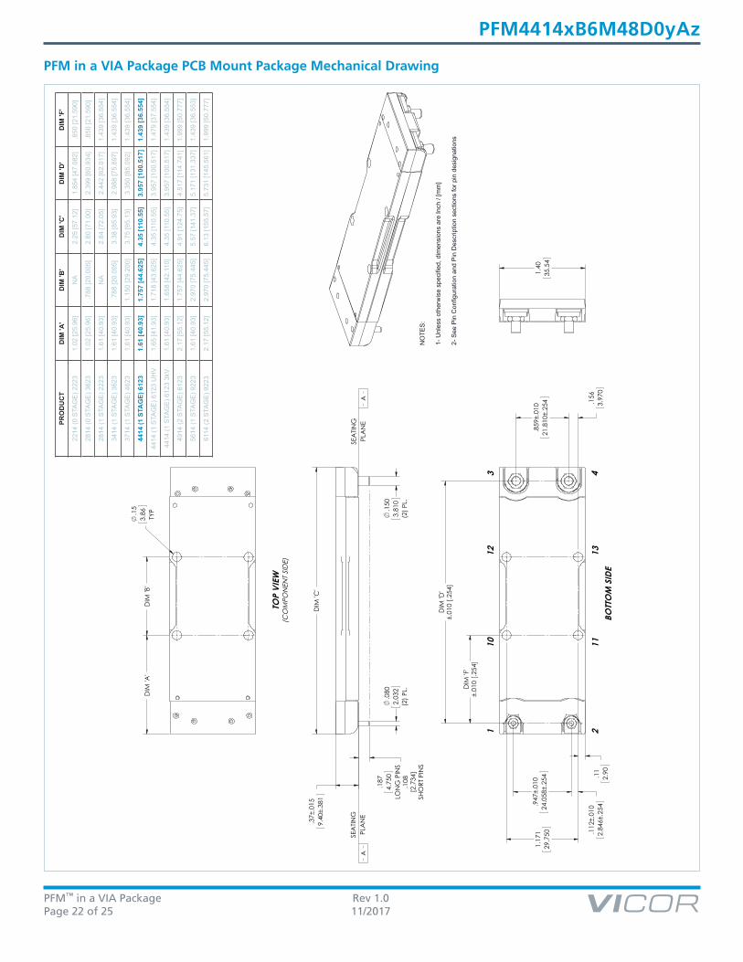
PFM™ in a VIA Package Rev 1.0Page 22 of 25 11/2017
PFM4414xB6M48D0yAz
BOTT
OM
SID
E
1 2
3 4
1012
1113
TOP
VIE
W(C
OM
PON
ENT
SID
E)
PFM in a VIA Package PCB Mount Package Mechanical DrawingPR
OD
UC
TD
IM 'A
'D
IM 'B
'D
IM 'C
'D
IM 'D
'D
IM 'F
'
2214
(0 S
TAG
E) 2
223
1.02
[25.
96]
NA
2.25
[57.
12]
1.85
4 [4
7.08
2]
.850
[21.
590]
2814
(0 S
TAG
E) 3
623
1.02
[25.
96]
.788
[20.
005]
2.
80 [7
1.00
] 2.
399
[60.
934]
.8
50 [2
1.59
0]
2814
(1 S
TAG
E) 2
223
1.61
[40.
93]
NA
2.84
[72.
05]
2.44
2 [6
2.01
7]
1.43
9 [3
6.55
4]
3414
(1 S
TAG
E) 3
623
1.61
[40.
93]
.788
[20.
005]
3.
38 [8
5.93
] 2.
988
[75.
897]
1.
439
[36.
554]
3714
(1 S
TAG
E) 4
623
1.61
[40.
93]
1.15
0 [2
9.20
0]
3.75
[95.
13]
3.35
0 [8
5.09
2]
1.43
9 [3
6.55
4]
4414
(1 S
TAG
E) 6
123
1.61
[40.
93]
1.75
7 [4
4.62
5]
4.35
[110
.55]
3.
957
[100
.517
] 1.
439
[36.
554]
4414
(1 S
TAG
E) 6
123
UH
V
1.65
[41.
93]
1.71
8 [4
3.62
5]
4.35
[110
.55]
3.
957
[100
.517
] 1.
479
[37.
554]
4414
(1 S
TAG
E) 6
123
3kV
1.
61 [4
0.93
] 1.
658
[42.
110]
4.
35 [1
10.5
5]
3.95
7 [1
00.5
17]
1.43
9 [3
6.55
4]
4914
(2 S
TAG
E) 6
123
2.17
[55.
12]
1.75
7 [4
4.62
5]
4.91
[124
.75]
4.
517
[114
.741
] 1.
999
[50.
777]
5614
(1 S
TAG
E) 9
223
1.61
[40.
93]
2.97
0 [7
5.44
5]
5.57
[141
.37]
5.
171
[131
.337
] 1.
439
[36.
553]
6114
(2 S
TAG
E) 9
223
2.17
[55.
12]
2.97
0 [7
5.44
5]
6.13
[155
.57]
5.
731
[145
.561
] 1.
999
[50.
777]
PFM™ in a VIA Package Rev 1.0Page 23 of 25 11/2017
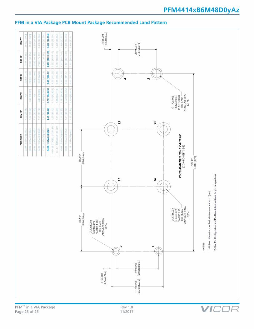
PFM4414xB6M48D0yAz
2 1
11 10
13 12
4 3
REC
OM
MEN
ED H
OLE
PA
TTER
N
PFM in a VIA Package PCB Mount Package Recommended Land PatternPR
OD
UC
TD
IM 'A
'D
IM 'B
'D
IM 'C
'D
IM 'D
'D
IM 'F
'
2214
(0 S
TAG
E) 2
223
1.02
[25.
96]
NA
2.25
[57.
12]
1.85
4 [4
7.08
2]
.850
[21.
590]
2814
(0 S
TAG
E) 3
623
1.02
[25.
96]
.788
[20.
005]
2.
80 [7
1.00
] 2.
399
[60.
934]
.8
50 [2
1.59
0]
2814
(1 S
TAG
E) 2
223
1.61
[40.
93]
NA
2.84
[72.
05]
2.44
2 [6
2.01
7]
1.43
9 [3
6.55
4]
3414
(1 S
TAG
E) 3
623
1.61
[40.
93]
.788
[20.
005]
3.
38 [8
5.93
] 2.
988
[75.
897]
1.
439
[36.
554]
3714
(1 S
TAG
E) 4
623
1.61
[40.
93]
1.15
0 [2
9.20
0]
3.75
[95.
13]
3.35
0 [8
5.09
2]
1.43
9 [3
6.55
4]
4414
(1 S
TAG
E) 6
123
1.61
[40.
93]
1.75
7 [4
4.62
5]
4.35
[110
.55]
3.
957
[100
.517
] 1.
439
[36.
554]
4414
(1 S
TAG
E) 6
123
UH
V
1.65
[41.
93]
1.71
8 [4
3.62
5]
4.35
[110
.55]
3.
957
[100
.517
] 1.
479
[37.
554]
4414
(1 S
TAG
E) 6
123
3kV
1.
61 [4
0.93
] 1.
658
[42.
110]
4.
35 [1
10.5
5]
3.95
7 [1
00.5
17]
1.43
9 [3
6.55
4]
4914
(2 S
TAG
E) 6
123
2.17
[55.
12]
1.75
7 [4
4.62
5]
4.91
[124
.75]
4.
517
[114
.741
] 1.
999
[50.
777]
5614
(1 S
TAG
E) 9
223
1.61
[40.
93]
2.97
0 [7
5.44
5]
5.57
[141
.37]
5.
171
[131
.337
] 1.
439
[36.
553]
6114
(2 S
TAG
E) 9
223
2.17
[55.
12]
2.97
0 [7
5.44
5]
6.13
[155
.57]
5.
731
[145
.561
] 1.
999
[50.
777]
PFM™ in a VIA Package Rev 1.0Page 24 of 25 11/2017
PFM4414xB6M48D0yAz
Revision History
Revision Date Description Page Number(s)
A 11/06/17 Initial release n/a

PFM™ in a VIA Package Rev 1.0Page 25 of 25 11/2017
PFM4414xB6M48D0yAz
Vicor’s comprehensive line of power solutions includes high density AC-DC and DC-DC modules and accessory components, fully configurable AC-DC and DC-DC power supplies, and complete custom power systems.
Information furnished by Vicor is believed to be accurate and reliable. However, no responsibility is assumed by Vicor for its use. Vicor makes no representations or warranties with respect to the accuracy or completeness of the contents of this publication. Vicor reserves the right to make changes to any products, specifications, and product descriptions at any time without notice. Information published by Vicor has been checked and is believed to be accurate at the time it was printed; however, Vicor assumes no responsibility for inaccuracies. Testing and other quality controls are used to the extent Vicor deems necessary to support Vicor’s product warranty. Except where mandated by government requirements, testing of all parameters of each product is not necessarily performed.
Specifications are subject to change without notice.
Visit http://www.vicorpower.com/ac-dc/converters/isolated-ac-dc-converter-pfc for the latest product information.
Vicor’s Standard Terms and Conditions and Product WarrantyAll sales are subject to Vicor’s Standard Terms and Conditions of Sale, and Product Warranty which are available on Vicor’s webpage (http://www.vicorpower.com/termsconditionswarranty) or upon request.
Life Support Policy
VICOR’S PRODUCTS ARE NOT AUTHORIZED FOR USE AS CRITICAL COMPONENTS IN LIFE SUPPORT DEVICES OR SYSTEMS WITHOUT THE EXPRESS PRIOR WRITTEN APPROVAL OF THE CHIEF EXECUTIVE OFFICER AND GENERAL COUNSEL OF VICOR CORPORATION. As used herein, life support devices or systems are devices which (a) are intended for surgical implant into the body, or (b) support or sustain life and whose failure to perform when properly used in accordance with instructions for use provided in the labeling can be reasonably expected to result in a significant injury to the user. A critical component is any component in a life support device or system whose failure to perform can be reasonably expected to cause the failure of the life support device or system or to affect its safety or effectiveness. Per Vicor Terms and Conditions of Sale, the user of Vicor products and components in life support applications assumes all risks of such use and indemnifies Vicor against all liability and damages.
Intellectual Property Notice
Vicor and its subsidiaries own Intellectual Property (including issued U.S. and Foreign Patents and pending patent applications) relating to the products described in this data sheet. No license, whether express, implied, or arising by estoppel or otherwise, to any intellectual property rights is granted by this document. Interested parties should contact Vicor’s Intellectual Property Department.
The products described on this data sheet are protected by the following U.S. Patents Numbers:Patents Pending.
Contact Us: http://www.vicorpower.com/contact-us
Vicor Corporation25 Frontage Road
Andover, MA, USA 01810Tel: 800-735-6200Fax: 978-475-6715
www.vicorpower.com
emailCustomer Service: [email protected]
Technical Support: [email protected]
©2017 Vicor Corporation. All rights reserved. The Vicor name is a registered trademark of Vicor Corporation.All other trademarks, product names, logos and brands are property of their respective owners.