is42s16100h is45s16100h - issi power supply for dq pin gndq ground for dq pin nc no connection...
TRANSCRIPT

Integrated Silicon Solution, Inc. — www.issi.com 1Rev. A110/11/2016
Copyright © 2016 Integrated Silicon Solution, Inc. All rights reserved. ISSI reserves the right to make changes to this specification and its products at any time without notice. ISSI assumes no liability arising out of the application or use of any information, products or services described herein. Customers are advised to obtain the latest version of this device specification before relying on any published information and before placing orders for products.
Integrated Silicon Solution, Inc. does not recommend the use of any of its products in life support applications where the failure or malfunction of the product can rea-sonably be expected to cause failure of the life support system or to significantly affect its safety or effectiveness. Products are not authorized for use in such applica-tions unless Integrated Silicon Solution, Inc. receives written assurance to its satisfaction, that:a.) the risk of injury or damage has been minimized;b.) the user assume all such risks; andc.) potential liability of Integrated Silicon Solution, Inc is adequately protected under the circumstances
IS42S16100HIS45S16100H
OCTOBER 2016
FEATURES• Clockfrequency:200,166,143MHz• Fullysynchronous;allsignalsreferencedtoa
positive clock edge• Twobankscanbeoperatedsimultaneouslyand
independently• DualinternalbankcontrolledbyA11(bankselect)• Single3.3Vpowersupply• LVTTLinterface• Programmableburstlength
–(1,2,4,8,fullpage)• Programmableburstsequence:
Sequential/Interleave• 2048refreshcyclesevery32ms(Com,Ind,A1
grade)or16ms(A2grade)• Randomcolumnaddresseveryclockcycle• ProgrammableCASlatency(2,3clocks)• Burstread/writeandburstread/singlewrite
operations capability• Burstterminationbyburststopand
precharge command• BytecontrolledbyLDQMandUDQM• Packages:400-mil50-pinTSOP-IIand60-ball
TF-BGA• TemperatureGrades:
Commercial(0oC to +70oC) Industrial(-40oCto+85oC)
AutomotiveA1(-40oCto+85oC)AutomotiveA2(-40oCto+105oC)
DESCRIPTIONISSI’s16MbSynchronousDRAMIS42/4516100Hisorganizedasa524,288-wordx16-bitx2-bankforimprovedperformance.ThesynchronousDRAMsachieve high-speed data transfer using pipeline architecture. All inputs and outputs signals refer to the rising edge of the clock input.
512K Words x 16 Bits x 2 Banks16Mb SYNCHRONOUS DYNAMIC RAM

IS42S16100H, IS45S16100H
2 Integrated Silicon Solution, Inc. — www.issi.com Rev. A1
10/11/2016
PIN CONFIGURATIONS50-Pin TSOP (Type II)
1
2
3
4
5
6
7
8
9
10
11
12
13
14
15
16
17
18
19
20
21
22
23
24
25
50
49
48
47
46
45
44
43
42
41
40
39
38
37
36
35
34
33
32
31
30
29
28
27
26
VDD
DQ0
DQ1
GNDQ
DQ2
DQ3
VDDQ
DQ4
DQ5
GNDQ
DQ6
DQ7
VDDQ
LDQM
WE
CAS
RAS
CS
A11
A10
A0
A1
A2
A3
VDD
GND
DQ15
DQ14
GNDQ
DQ13
DQ12
VDDQ
DQ11
DQ10
GNDQ
DQ9
DQ8
VDDQ
NC
UDQM
CLK
CKE
NC
A9
A8
A7
A6
A5
A4
GND
PIN DESCRIPTIONSA0-A10 RowAddressInput
A11 BankSelectAddress
A0-A7 Column Address Input
DQ0toDQ15 DataDQ
CLK SystemClockInput
CKE ClockEnable
CS Chip Select
RAS RowAddress Strobe Command
CAS Column Address Strobe Command
WE WriteEnable
LDQM LowerBye,Input/OutputMask
UDQM UpperBye,Input/OutputMask
VDD Power
GND Ground
VDDQ PowerSupplyforDQPin
GNDQ GroundforDQPin
NC NoConnection

Integrated Silicon Solution, Inc. — www.issi.com 3Rev. A110/11/2016
IS42S16100H, IS45S16100H
PIN CONFIGURATIONpackage code: B 60 BaLL Tf-Bga (Top View) (10.1 mm x 6.4 mm Body, 0.65 mm Ball pitch)
1 2 3 4 5 6 7
A
B
C
D
E
F
G
H
J
K
L
M
N
P
R
GND
DQ14
DQ13
DQ12
DQ10
DQ9
DQ8
NC
NC
NC
CKE
A11
A8
A6
GND
DQ15
GND
VDDQ
DQ11
GNDQ
VDDQ
NC
NC
UDQM
CLK
NC
A9
A7
A5
A4
DQ0
VDDQ
GNDQ
DQ4
VDDQ
GNDQ
NC
VDD
LDQM
RAS
NC
NC
A0
A2
A3
VDD
DQ1
DQ2
DQ3
DQ5
DQ6
DQ7
NC
WE
CAS
CS
NC
A10
A1
VDD
PIN DESCRIPTIONSa0-a10 Row address Inputa0-a7 column address Inputa11 Bank Select addressdQ0 to dQ15 data I/ocLk System clock Inputcke clock enableCS chip SelectRAS Row address Strobe commandCAS column address Strobe command
WE Write enableLdQM, UdQM x16 Input/output MaskVdd powergNd groundVddq power Supply for I/o pingNdq ground for I/o pinNc No connection

IS42S16100H, IS45S16100H
4 Integrated Silicon Solution, Inc. — www.issi.com Rev. A1
10/11/2016
PIN FUNCTIONS
TSOP Pin No. Symbol Type Function (In Detail)
20to24 A0-A10 InputPin A0 to A10 are address inputs. A0-A10 are used as row address inputs during active
27to32 commandinputandA0-A7ascolumnaddressinputsduringreadorwritecommandinput.A10 is also used to determine the precharge mode during other commands. If A10 is LOWduringprechargecommand,thebankselectedbyA11isprecharged,butifA10isHIGH,bothbankswillbeprecharged. WhenA10isHIGHinreadorwritecommandcycle,theprechargestartsautomaticallyafter the burst access. ThesesignalsbecomepartoftheOPCODEduringmoderegistersetcommandinput.
19 A11 InputPin A11isthebankselectionsignal.WhenA11isLOW,bank0isselectedandwhenhigh,bank1isselected.ThissignalbecomespartoftheOPCODEduringmoderegistersetcommand input.
16 CAS Input Pin CAS, in conjunction with the RAS and WE, forms the device command. See the “CommandTruthTable”itemfordetailsondevicecommands.
34 CKE InputPin TheCKEinputdetermineswhethertheCLKinputisenabledwithinthedevice.WhenisCKEHIGH,thenextrisingedgeoftheCLKsignalwillbevalid,andwhenLOW,invalid.WhenCKEisLOW,thedevicewillbeineitherthepower-downmode,theclocksuspendmode,ortheselfrefreshmode.TheCKEisanasynchronousinput.
35 CLK InputPin CLKisthemasterclockinputforthisdevice.ExceptforCKE,allinputstothisdeviceareacquired in synchronization with the rising edge of this pin.
18 CS InputPin TheCS input determines whether command input is enabled within the device. Command input is enabled when CSisLOW,anddisabledwithCSisHIGH.Thedeviceremains in the previous state when CSisHIGH.
2,3,5,6,8,9,11 DQ0to DQPin DQ0toDQ15areDQpins.DQthroughthesepinscanbecontrolledinbyteunits
12,39,40,42,43, DQ15 usingtheLDQMandUDQMpins.
45,46,48,49
14,36 LDQM, InputPin LDQMandUDQMcontrolthelowerandupperbytesoftheDQbuffers.Inread
UDQM mode,LDQMandUDQMcontroltheoutputbuffer.WhenLDQMorUDQMisLOW,thecorrespondingbufferbyteisenabled,andwhenHIGH,disabled.Theoutputsgo totheHIGHimpedancestatewhenLDQM/UDQMisHIGH.ThisfunctioncorrespondstoOE inconventionalDRAMs.Inwritemode,LDQMandUDQMcontroltheinputbuffer.WhenLDQMorUDQMisLOW,thecorrespondingbufferbyteisenabled,anddatacanbewrittentothedevice.WhenLDQMorUDQMisHIGH,inputdataismaskedandcannotbewritten to the device.
17 RAS Input Pin RAS, in conjunction with CAS and WE, forms the device command. See the “Command TruthTable”itemfordetailsondevicecommands.
15 WE Input Pin WE, in conjunction with RAS and CAS, forms the device command. See the “Command TruthTable”itemfordetailsondevicecommands.
7,13,38,44 VDDQ PowerSupplyPin VDDQistheoutputbufferpowersupply.
1,25 VDD PowerSupplyPin VDD is the device internal power supply.
4,10,41,47 GNDQ PowerSupplyPin GNDQistheoutputbufferground.
26,50 GND PowerSupplyPin GND is the device internal ground.
Integrated Silicon Solution, Inc. — www.issi.com 5Rev. A110/11/2016
IS42S16100H, IS45S16100H
FUNCTIONAL BLOCK DIAGRAM
CLKCKE
CSRASCASWEA11
A9A8A7A6A5A4A3A2A1A0
A10
COMMANDDECODER
&CLOCK
GENERATOR MODEREGISTER
REFRESHCONTROLLER
REFRESHCOUNTER
SELF
REFRESH
CONTROLLER
ROWADDRESS
LATCH MU
LTIP
LE
XE
R
ROWADDRESSBUFFER
ROWADDRESSBUFFER
CO
LU
MN
AD
DR
ES
S L
AT
CH
BU
RS
T C
OU
NT
ER
CO
LU
MN
AD
DR
ES
S B
UF
FE
RR
OW
DE
CO
DE
RR
OW
DE
CO
DE
R
MEMORY CELLARRAY
BANK 0
COLUMN DECODER
MEMORY CELLARRAY
BANK 1
DATA INBUFFER
DATA OUTBUFFER
SENSE AMP I/O GATE
SENSE AMP I/O GATE
2048
2048
DQM
DQ 0-15
VDD/VDDQ
GND/GNDQ
11
11
11 11
8
11 11
8
16
16 16
16 256
256

IS42S16100H, IS45S16100H
6 Integrated Silicon Solution, Inc. — www.issi.com Rev. A1
10/11/2016
ABSOLUTE MAXIMUM RATINGS(1)
Symbol Parameters Rating Unit
VDD max MaximumSupplyVoltage –1.0to+4.6 V
VDDq max MaximumSupplyVoltageforOutputBuffer –1.0to+4.6 V
ViN InputVoltage –1.0to+4.6 V
Vout OutputVoltage –1.0to+4.6 V
PD max AllowablePowerDissipation 1 W
Ics outputShortedCurrent 50 mA
Topr operatingTemperature Commerical 0to+70 °C Industrial -40to+85 °C A1 -40to+85 °C A2 -40to+105 °C
Tstg StorageTemperature –55to+150 °C
DC RECOMMENDED OPERATING CONDITION(2) (AtTa = 0oC to +70oCforCommercialtemperature,Ta=-40oCto+85oCforIndustrialandA1temperature,Ta=-40oC to +105oC for A2 temperature)
Symbol Parameter Min. Typ. Max. Unit
VDD, VDDq SupplyVoltage 3.0 3.3 3.6 V Vih InputHighVoltage(3) 2.0 — VDD +0.3 V Vil InputLowVoltage(4) -0.3 — +0.8 V
CAPACITANCE CHARACTERISTICS(1,2) (AtTa=0to+25°C,VDD=VDDQ=3.3±0.3V,f=1MHz)
Symbol Parameter Typ. Max. Unit
CiN1 InputCapacitance:A0-A11 — 4 pF CiN2 InputCapacitance:(CLK,CKE, CS, RAS, CAS, WE,LDQM,UDQM) — 4 pF CI/O DataInput/OutputCapacitance:DQ0-DQ15 — 5 pFNotes:1.StressgreaterthanthoselistedunderABSOLUTEMAXIMUMRATINGSmaycausepermanentdamagetothedevice.Thisisa
stress rating only and functional operation of the device at these or any other conditions above those indicated in the operational sectionsofthisspecificationisnotimplied.Exposuretoabsolutemaximumratingconditionsforextendedperiodsmayaffectreli-ability.
2.AllvoltagesarereferencedtoGND.3.Vih(max)=VDDq+1.2Vwithapulsewidth≤3ns.4.Vil(min)=VDDq-1.2Vwithapulsewidth≤3ns.

Integrated Silicon Solution, Inc. — www.issi.com 7Rev. A110/11/2016
IS42S16100H, IS45S16100H
DC ELECTRICAL CHARACTERISTICS (RecommendedOperationConditionsunlessotherwisenoted.)
Symbol Parameter Test Condition Speed Min. Max. Unit
iil InputLeakageCurrent 0V≤ViN ≤VDD, with pins other than –5 5 µA thetestedpinat0V
iol OutputLeakageCurrent Outputisdisabled,0V≤ Vout ≤VDD –5 5 µA
Voh OutputHighVoltageLevel iout=–2mA 2.4 — V
Vol OutputLowVoltageLevel iout=+2mA — 0.4 V
icc1 OperatingCurrent(1,2) OneBankOperation, CASlatency=3 Com. -5 — 60 mA
BurstLength=1 Com. -6 — 55
trc ≥ trc(min.) Com. -7 — 50
Iout = 0mA Ind, A1 -6 — 60 A2 -6 — 65 Ind,A1 -7 — 55 A2 -7 — 60
icc2p PrechargeStandbyCurrentCKE≤ Vil(max) tck=15ns Com — — 3 mA Ind,A1 — — 4
Icc2ps (InPower-DownMode) tck = ∞ Com — — 2 m A Ind,A1 — — 3.5 A2 — — 3.5
icc3N ActiveStandbyCurrent CKE≥ Vih(miN) tck=15ns — — 40 mA Icc3Ns (InNonPower-DownMode) tck = ∞ Com — — 30 mA Ind,A1 — — 30 A2 — — 30
icc4 OperatingCurrent tck = tck(miN) CASlatency=3 Com -5 — 80 mA (InBurstMode)(1) Iout = 0mA Com -6 — 70 Ind,A1 -6 — 80 A2 -6 — 90 Com -7 — 60 Ind, A1 -7 — 70 A2 -7 — 80
CAS latency = 2 Com -5 — 80 mA Com -6 — 70 Ind,A1 -6 — 80 A2 -6 — 90 Com -7 — 60 Ind, A1 -7 — 70 A2 -7 — 80
Notes:1.Thesearethevaluesattheminimumcycletime.Sincethecurrentsaretransient,thesevaluesdecreaseasthecycletimein-
creases.Alsonotethatabypasscapacitorofatleast0.01µFshouldbeinsertedbetweenVDD andGNDforeachmemorychiptosuppresspowersupplyvoltagenoise(voltagedrops)duetothesetransientcurrents.
2. Icc1 and Icc4dependontheoutputload.ThemaximumvaluesforIcc1 and Icc4 are obtained with the output open state.

IS42S16100H, IS45S16100H
8 Integrated Silicon Solution, Inc. — www.issi.com Rev. A1
10/11/2016
DC ELECTRICAL CHARACTERISTICS (RecommendedOperationConditionsunlessotherwisenoted.)
Symbol Parameter Test Condition Speed Min. Max. Unit
icc5 Auto-RefreshCurrent trc = trc (miN) CASlatency=3 Com. -5 — 50 mA Com. -6 — 45 Ind,A1 -6 — 50 A2 -6 — 55 Com -7 — 40 Ind,A1 -7 — 45 A2 -7 — 50
CASlatency=2 Com -5 — 50 mA Com -6 — 45 Ind,A1 -6 — 50 A2 -6 — 55
Com -7 — 40 Ind,A1 -7 — 45 A2 -7 — 50
icc6 Self-RefreshCurrent CKE≤0.2V — — 2 mA
Notes:1.Thesearethevaluesattheminimumcycletime.Sincethecurrentsaretransient,thesevaluesdecreaseasthecycletimein-
creases.Alsonotethatabypasscapacitorofatleast0.01µFshouldbeinsertedbetweenVDD andGNDforeachmemorychiptosuppresspowersupplyvoltagenoise(voltagedrops)duetothesetransientcurrents.
2. Icc1 and Icc4dependontheoutputload.ThemaximumvaluesforIcc1 and Icc4 are obtained with the output open state.

Integrated Silicon Solution, Inc. — www.issi.com 9Rev. A110/11/2016
IS42S16100H, IS45S16100H
AC CHARACTERISTICS(1,2,3)
-5 -6 -7 Symbol Parameter Min. Max. Min. Max. Min. Max. Units
tck3 ClockCycleTime CASLatency=3 5 — 6 — 7 — ns tck2 CASLatency=2 8 — 8 — 8 — ns
tac3 AccessTimeFromCLK(4) CASLatency=3 — 5 — 5.5 — 5.5 ns tac2 CASLatency=2 — 6 — 6 — 6 ns
tchi CLKHIGHLevelWidth 2 — 2.5 — 2.5 — ns
tcl CLKLOWLevelWidth 2 — 2.5 — 2.5 — ns
toh3 OutputDataHoldTime CASLatency=3 2 — 2.0 — 2.0 — ns toh2 CAS Latency=2 2.5 — 2.5 — 2.5 — ns
tlz OutputLOWImpedanceTime 0 — 0 — 0 — ns
thz3 OutputHIGHImpedanceTime(5) CASLatency=3 — 5 — 5.5 — 5.5 ns thz2 CASLatency=2 — 6 — 6 — 6 ns
tDs InputDataSetupTime 2 — 2 — 2 — ns
tDh InputDataHoldTime 1 — 1 — 1 — ns
tas AddressSetupTime 2 — 2 — 2 — ns
tah AddressHoldTime 1 — 1 — 1 — ns
tcks CKESetupTime 2 — 2 — 2 — ns
tckh CKEHoldTime 1 — 1 — 1 — ns
tcka CKEtoCLKRecoveryDelayTime 1CLK+3 — 1CLK+3 — 1CLK+3 — ns
tcs CommandSetupTime(CS, RAS, CAS, WE,DQM) 2 — 2 — 2 — ns
tch CommandHoldTime(CS, RAS, CAS, WE,DQM) 1 — 1 — 1 — ns
trc CommandPeriod(REFtoREF/ACTtoACT) 50 — 54 — 63 — ns
tras CommandPeriod(ACTtoPRE) 35 100,000 36 100,000 42 100,000 ns
trp CommandPeriod(PREtoACT) 15 — 18 — 21 — ns
trcD ActiveCommandToRead/WriteCommandDelayTime 15 — 18 — 21 — ns
trrD CommandPeriod(ACT[0]toACT[1]) 10 — 12 — 14 — ns
tDpl3 InputDataToPrecharge CASLatency=3 2CLK — 2CLK — 2CLK — ns CommandDelaytime tDpl2 CAS Latency=2 2CLK — 2CLK — 2CLK — ns
tDal3 InputDataToActive/Refresh CASLatency=3 2CLK+trp — 2CLK+trp — 2CLK+trp — ns CommandDelaytime(DuringAuto-Precharge) tDal2 CAS Latency=2 2CLK+trp — 2CLK+trp — 2CLK+trp — ns
txsr ExitSelf-RefreshtoActiveTime 55 — 60 — 70 — ns
tt TransitionTime 0.3 1.2 0.3 1.2 0.3 1.2 ns
tref RefreshCycleTime(2048)fortemperatureTa ≤85oC — 32 — 32 — 32 ms
tref RefreshCycleTime(2048)fortemperatureTa >85oC(A2only)6 — — — — — 16 msNotes:1.Whenpowerisfirstapplied,memoryoperationshouldbestarted100µsafterVDD andVDDq reach their stipulated voltages. Also note that the power-on sequence must be executed before starting memory operation.2. measured with tt = 1 ns. If clock rising time is longer than 1ns, (tt/2 - 0.5)ns should be added to the parameter.3.Thereferencelevelis1.4Vwhenmeasuringinputsignaltiming.RiseandfalltimesaremeasuredbetweenVih (min.)andVil (max.).4.Accesstimeismeasuredat1.4Vwiththeloadshowninthefigurebelow.5.Thetimethz (max.)isdefinedasthetimerequiredfortheoutputvoltagetotransitionby±200mVfromVoh (min.)orVol(max.)whenthe output is in the high impedance state.6.Self-RefreshModeisnotsupportedforA2gradewithTa>85oC.

IS42S16100H, IS45S16100H
10 Integrated Silicon Solution, Inc. — www.issi.com Rev. A1
10/11/2016
OPERATING FREQUENCY / LATENCY RELATIONSHIPS (CAS Latency=3)
SYMBOL PARAMETER -5 -6 -7 UNITS
— ClockCycleTime 5 6 7 ns
— OperatingFrequency 200 166 143 MHz
tcac CASLatency 3 3 3 cycle
trcD ActiveCommandToRead/WriteCommandDelayTime 3 3 3 cycle
trac RASLatency(trcD + tcac) 6 6 6 cycle
trc CommandPeriod(REFtoREF/ACTtoACT) 10 9 9 cycle
tras CommandPeriod(ACTtoPRE) 7 6 6 cycle
trp CommandPeriod(PREtoACT) 3 3 3 cycle
trrD CommandPeriod(ACT[0]toACT[1]) 2 2 2 cycle
tccD ColumnCommandDelayTime 1 1 1 cycle (READ,READA,WRIT,WRITA)
tDpl InputDataToPrechargeCommandDelayTime 2 2 2 cycle
tDal InputDataToActive/RefreshCommandDelayTime 5 5 5 cycle (DuringAuto-Precharge)
trbD BurstStopCommandToOutputinHIGH-ZDelayTime 3 3 3 cycle (Read)
twbD BurstStopCommandToInputinInvalidDelayTime 0 0 0 cycle (Write)
trql PrechargeCommandToOutputinHIGH-ZDelayTime 3 3 3 cycle (Read)
twDl PrechargeCommandToInputinInvalidDelayTime 0 0 0 cycle (Write)
tpql LastOutputToAuto-PrechargeStartTime(Read) –2 –2 –2 cycle
tqmD DQMToOutputDelayTime(Read) 2 2 2 cycle
tDmD DQMToInputDelayTime(Write) 0 0 0 cycle
tmcD ModeRegisterSetToCommandDelayTime 2 2 2 cycle
AC TEST CONDITIONS (Input/OutputReferenceLevel:1.4V)
I/O
50 Ω
+1.4V
50 pF
Output LoadInput
tOH tAC
1.4V 1.4V
tCHtCS
tCKtCHI tCL
2.8V
1.4V
0.0V
2.8V
1.4V
0.0V
CLK
INPUT
OUTPUT

Integrated Silicon Solution, Inc. — www.issi.com 11Rev. A110/11/2016
IS42S16100H, IS45S16100H
COMMANDS
CLK
CKE HIGH
ROW
ROW
BANK 1
BANK 0
CS
RAS
CAS
WE
A0-A9
A10
A11
CLK
CKE HIGH
COLUMN
BANK 1
AUTO PRECHARGE
NO PRECHARGE
BANK 0
CS
RAS
CAS
WE
A0-A9
A10
A11
(1)
CLK
CKE HIGH
COLUMN
AUTO PRECHARGE
BANK 1
BANK 0
CS
RAS
CAS
WE
A0-A9
A10
A11
CLK
CKE HIGH
BANK 1
BANK 0 AND BANK 1
BANK 0 OR BANK 1NO PRECHARGE
BANK 0
CS
RAS
CAS
WE
A0-A9
A10
A11
(1)
Notes: 1.A8-A9=Don’tCare.
Don't Care
Active Command Read Command
Write Command Precharge Command

IS42S16100H, IS45S16100H
12 Integrated Silicon Solution, Inc. — www.issi.com Rev. A1
10/11/2016
COMMANDS (cont.)
CLK
CKE HIGH
CS
RAS
CAS
WE
A0-A9
A10
A11
CLK
CKE HIGH
CS
RAS
CAS
WE
A0-A9
A10
A11
CLK
CKE HIGH
CS
RAS
CAS
WE
A0-A9
A10
A11
CLK
CKE HIGH
CS
RAS
CAS
WE
A0-A9
A10
A11
OP-CODE
OP-CODE
OP-CODE
Don't Care
No-Operation Command Device Deselect Command
Mode Register Set Command Auto-Refresh Command

Integrated Silicon Solution, Inc. — www.issi.com 13Rev. A110/11/2016
IS42S16100H, IS45S16100H
COMMANDS (cont.)
CLK
CKE
CS
RAS
CAS
WE
A0-A9
A10
A11
CLK
CKE
CS
RAS
CAS
WE
A0-A9
A10
A11
BANK(S) ACTIVE HIGH
NOP
NOP
NOP
NOP
CLK
CKE
CS
RAS
CAS
WE
A0-A9
A10
A11
CLK
CKE
CS
RAS
CAS
WE
A0-A9
A10
A11
ALL BANKS IDLE
NOP
NOP
NOP
NOP
Self-Refresh Command Power Down Command
Clock Suspend Command Burst Stop Command

IS42S16100H, IS45S16100H
14 Integrated Silicon Solution, Inc. — www.issi.com Rev. A1
10/11/2016
Mode Register Set Command(CS, RAS, CAS, WE=LOW)
The IS42/4516100H product incorporates a registerthatdefinesthedeviceoperatingmode.Thiscommandfunctions as a data input pin that loads this register from the pins A0 to A11. When power is first applied, the stipulated power-on sequence should be executed and thentheIS42/4516100Hshouldbeinitializedbyexecutinga mode register set command.
Note that the mode register set command can beexecutedonlywhenbothbanksareintheidlestate(i.e.deactivated).
Another command cannot be executed after a mode register set command until after the passage of the period tmcD, which is the period required for mode register set command execution.
Active Command (CS, RAS=LOW,CAS, WE=HIGH)
TheIS42/4516100Hincludestwobanksof2048rowseach.Thiscommandselectsoneofthetwobanksaccordingto the A11 pin and activates the row selected by the pins A0 to A10.
ThiscommandcorrespondstothefalloftheRAS signal fromHIGHtoLOWinconventionalDRAMs.
Precharge Command (CS, RAS, WE=LOW,CAS=HIGH)
ThiscommandstartsprechargingthebankselectedbypinsA10andA11.WhenA10isHIGH,bothbanksareprecharged at the same time.When A10 is LOW, thebank selected by A11 is precharged. After executing this command,thenextcommandfor theselectedbank(s)is executed after passage of the period trp, which is the period required for bank precharging.
ThiscommandcorrespondstotheRASsignalfromLOWtoHIGHinconventionalDRAMs
Read Command (CS, CAS=LOW,RAS, WE=HIGH)
ThiscommandselectsthebankspecifiedbytheA11pinand starts a burst read operation at the start address specifiedbypinsA0toA9.DataisoutputfollowingCAS latency.
Theselectedbankmustbeactivatedbeforeexecutingthis command.
WhentheA10pinisHIGH,thiscommandfunctionsasaread with auto-precharge command. After the burst read completes, the bank selected by pin A11 is precharged. WhentheA10pinisLOW,thebankselectedbytheA11pin remains in the activated state after the burst read completes.
Write Command(CS, CAS, WE=LOW,RAS=HIGH)
When burst write mode has been selected with the mode register set command, this command selects the bank specified by the A11 pin and starts a burst write operation atthestartaddressspecifiedbypinsA0toA9.ThisfirstdatamustbeinputtotheDQpinsinthecycleinwhichthis command.
The selected bank must be activated before executingthis command.
When A10 pin is HIGH, this command functions as awrite with auto-precharge command. After the burst write completes, the bank selected by pin A11 is precharged. When the A10 pin is low, the bank selected by the A11 pin remains in the activated state after the burst write completes.
After the input of the last burst write data, the application mustwaitforthewriterecoveryperiod(tDpl, tDal) to elapse according to CAS latency.
Auto-Refresh Command(CS, RAS, CAS=LOW,WE,CKE=HIGH)
Thiscommandexecutestheauto-refreshoperation.Therow address and bank to be refreshed are automatically generated during this operation.
Bothbanksmustbeplacedintheidlestatebeforeexecutingthis command.
Thestipulatedperiod(trc) is required for a single refresh operation, and no other commands can be executed during this period.
Thedevicegoestotheidlestateaftertheinternalrefreshoperation completes.
Thiscommandmustbeexecutedperiodicallyaccordingto trefspecification(ACCharacteristics).
This command corresponds to CBR auto-refresh inconventionalDRAMs.

Integrated Silicon Solution, Inc. — www.issi.com 15Rev. A110/11/2016
IS42S16100H, IS45S16100H
Self-Refresh Command(CS, RAS, CAS,CKE=LOW,WE=HIGH)
Thiscommandexecutestheself-refreshoperation.Therow address to be refreshed, the bank, and the refresh interval are generated automatically internally during this operation.Theself-refreshoperationisstartedbydroppingtheCKEpinfromHIGHtoLOW.Theself-refreshoperationcontinuesaslongastheCKEpinremainsLOWandthereis no need for external control of any other pins.The self-refreshoperationisterminatedbyraisingtheCKEpin fromLOWtoHIGH.Thenextcommandcannotbeexecuteduntilthedeviceinternalrecoveryperiod(txsr) has elapsed. After the self-refresh, since it is impossible to determine the address of the last row to be refreshed, an auto-refresh should immediately be performed for all addresses(4096cycles).
Bothbanksmustbeplacedintheidlestatebeforeexecutingthis command.
Burst Stop Command (CS, WE,=LOW,RAS, CAS=HIGH)
Thecommandforcibly terminatesburst readandwriteoperations. When this command is executed during a burst read operation, data output stops after the CAS latency period has elapsed.
No Operation(CS,=LOW,RAS, CAS, WE=HIGH)
Thiscommandhasnoeffectonthedevice.
Device Deselect Command (CS=HIGH)
Thiscommanddoesnotselectthedeviceforanobjectofoperation. In other words, it performs no operation with respect to the device.
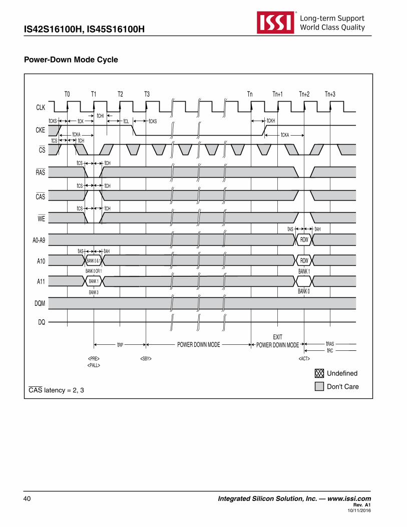
Power-Down Command(CKE=LOW)
Whenbothbanksareintheidle(inactive)state,orwhenatleastoneofthebanksisnotintheidle(inactive)state,this command can be used to suppress device power dissipation by reducing device internal operations to the absolute minimum. Power-down mode is started by droppingtheCKEpinfromHIGHtoLOW.Power-downmodecontinuesaslongastheCKEpinisheldlow.AllpinsotherthantheCKEpinareinvalidandnoneoftheothercommandscanbeexecutedinthismode.Thepower-downoperationisterminatedbyraisingtheCKEpinfromLOWtoHIGH.Thenextcommandcannotbeexecuteduntiltherecoveryperiod(tcka) has elapsed.
Since this command differs from the self-refresh command described above in that the refresh operation is not performed automatically internally, the refresh operation mustbeperformedwithintherefreshperiod(tref).Thusthe maximum time that power-down mode can be held is just under the refresh cycle time.
Clock Suspend(CKE=LOW)
Thiscommandcanbeusedtostopthedevice internalclock temporarily during a read or write cycle. Clock suspendmodeisstartedbydroppingtheCKEpinfromHIGHtoLOW.ClocksuspendmodecontinuesaslongastheCKEpinisheldLOW.AllinputpinsotherthantheCKEpin are invalid and none of the other commands can be executed in this mode. Also note that the device internal state is maintained. Clock suspend mode is terminated byraisingtheCKEpinfromLOWtoHIGH,atwhichpointdeviceoperationrestarts.Thenextcommandcannotbeexecuteduntiltherecoveryperiod(tcka) has elapsed.
Since this command differs from the self-refresh command described above in that the refresh operation is not performed automatically internally, the refresh operation mustbeperformedwithintherefreshperiod(tref).Thusthe maximum time that clock suspend mode can be held is just under the refresh cycle time.

IS42S16100H, IS45S16100H
16 Integrated Silicon Solution, Inc. — www.issi.com Rev. A1
10/11/2016
COMMAND TRUTH TABLE(1,2)
CKE Symbol Command n-1 n CS RAS CAS WE DQM A11 A10 A9-A0 I/On
MRS ModeRegisterSet(3,4) H X L L L L X OPCODE X REF Auto-Refresh(5) H H L L L H X X X X HIGH-Z SREF Self-Refresh(5,6) H L L L L H X X X X HIGH-Z PRE PrechargeSelectedBank H X L L H L X BS L X X PALL PrechargeBothBanks H X L L H L X X H X X ACT BankActivate(7) H X L L H H X BS Row Row X WRIT Write H X L H L L X BS L Column(18) X WRITA WriteWithAuto-Precharge(8) H X L H L L X BS H Column(18) X READ Read(8) H X L H L H X BS L Column(18) X READA ReadWithAuto-Precharge(8) H X L H L H X BS HColumn(18) X BST BurstStop(9) H X L H H L X X X X X NOP NoOperation H X L H H H X X X X X DESL DeviceDeselect H X H X X X X X X X X SBY ClockSuspend/StandbyMode L X X X X X X X X X X ENB DataWrite/OutputEnable H X X X X X L X X X Active MASK DataMask/OutputDisable H X X X X X H X X X HIGH-Z
DQM TRUTH TABLE(1,2)
CKE DQM Symbol Command n-1 n UPPER LOWER
ENB DataWrite/OutputEnable H X L L MASK DataMask/OutputDisable H X H H ENBU UpperByteDataWrite/OutputEnable H X L X ENBL LowerByteDataWrite/OutputEnable H X X L MASKU UpperByteDataMask/OutputDisable H X H X MASKL LowerByteDataMask/OutputDisable H X X H
CKE TRUTH TABLE(1,2)
CKE Symbol Command Current State n-1 n CS RAS CAS WE A11 A10 A9-A0
SPND StartClockSuspendMode Active H L X X X X X X X — ClockSuspend OtherStates L L X X X X X X X — TerminateClockSuspendMode ClockSuspend L H X X X X X X X REF Auto-Refresh Idle H H L L L H X X X SELF StartSelf-RefreshMode Idle H L L L L H X X X SELFX TerminateSelf-RefreshMode Self-Refresh L H L H H H X X X L H H X X X X X X PDWN StartPower-DownMode Idle H L L H H H X X X H L H X X X X X X — TerminatePower-DownMode Power-Down L H X X X X X X X

Integrated Silicon Solution, Inc. — www.issi.com 17Rev. A110/11/2016
IS42S16100H, IS45S16100H
OPERATION COMMAND TABLE(1,2)
Current State Command Operation CS RAS CAS WE A11 A10 A9-A0
Idle DESL NoOperationorPower-Down(12) H X X X X X X NOP NoOperationorPower-Down(12) L H H H X X X BST NoOperationorPower-Down L H H L X X X READ/READA Illegal L H L H V V V(18)
WRIT/WRITA Illegal L H L L V V V(18)
ACT RowActive L L H H V V V(18)
PRE/PALL NoOperation L L H L V V X REF/SELF Auto-RefreshorSelf-Refresh(13) L L L H X X X MRS ModeRegisterSet L L L L OPCODE RowActive DESL NoOperation H X X X X X X NOP NoOperation L H H H X X X BST NoOperation L H H L X X X READ/READA ReadStart(17) L H L H V V V(18)
WRIT/WRITA WriteStart(17) L H L L V V V(18)
ACT Illegal(10) L L H H V V V(18)
PRE/PALL Precharge(15) L L H L V V X REF/SELF Illegal L L L H X X X MRS Illegal L L L L OPCODE Read DESL BurstReadContinues,RowActiveWhenDone H X X X X X X NOP BurstReadContinues,RowActiveWhenDone L H H H X X X BST BurstInterrupted,RowActiveAfterInterrupt L H H L X X X READ/READA BurstInterrupted,ReadRestartAfterInterrupt(16) L H L H V V V(18)
WRIT/WRITA BurstInterruptedWriteStartAfterInterrupt(11,16) L H L L V V V(18)
ACT Illegal(10) L L H H V V V(18)
PRE/PALL BurstReadInterrupted,PrechargeAfterInterrupt L L H L V V X REF/SELF Illegal L L L H X X X MRS Illegal L L L L OPCODE Write DESL BurstWriteContinues,WriteRecoveryWhenDone H X X X X X X NOP BurstWriteContinues,WriteRecoveryWhenDone L H H H X X X BST BurstWriteInterrupted,RowActiveAfterInterrupt L H H L X X X READ/READA BurstWriteInterrupted,ReadStartAfterInterrupt(11,16) L H L H V V V(18)
WRIT/WRITA BurstWriteInterrupted,WriteRestartAfterInterrupt(16) L H L L V V V(18)
ACT Illegal(10) L L H H V V V(18)
PRE/PALL BurstWriteInterrupted,PrechargeAfterInterrupt L L H L V V X REF/SELF Illegal L L L H X X X MRS Illegal L L L L OPCODE ReadWith DESL BurstReadContinues,PrechargeWhenDone H X X X X X X Auto- NOP BurstReadContinues,PrechargeWhenDone L H H H X X X Precharge BST Illegal L H H L X X X READ/READA Illegal L H L H V V V(18)
WRIT/WRITA Illegal L H L L V V V(18)
ACT Illegal(10) L L H H V V V(18)
PRE/PALL Illegal(10) L L H L V V X REF/SELF Illegal L L L H X X X MRS Illegal L L L L OPCODE

IS42S16100H, IS45S16100H
18 Integrated Silicon Solution, Inc. — www.issi.com Rev. A1
10/11/2016
OPERATION COMMAND TABLE(1,2)
Current State Command Operation CS RAS CAS WE A11 A10 A9-A0
Write With DESL BurstWriteContinues,WriteRecoveryAndPrecharge H X X X X X X Auto-Precharge WhenDone
NOP BurstWriteContinues,WriteRecoveryAndPrecharge L H H H X X X
BST Illegal L H H L X X X READ/READA Illegal L H L H V V V(18)
WRIT/WRITA Illegal L H L L V V V(18)
ACT Illegal(10) L L H H V V V(18)
PRE/PALL Illegal(10) L L H L V V X REF/SELF Illegal L L L H X X X MRS Illegal L L L L OPCODERowPrecharge DESL NoOperation,IdleStateAftertrpHasElapsed H X X X X X X NOP NoOperation,IdleStateAftertrp HasElapsed L H H H X X X BST NoOperation,IdleStateAftertrpHasElapsed L H H L X X X
READ/READA Illegal(10) L H L H V V V(18)
WRIT/WRITA Illegal(10) L H L L V V V(18)
ACT Illegal(10) L L H H V V V(18)
PRE/PALL NoOperation,IdleStateAftertrpHasElapsed(10) L L H L V V X REF/SELF Illegal L L L H X X X MRS Illegal L L L L OPCODE Immediately DESL NoOperation,RowActiveAftertrcDHasElapsed H X X X X X X Following NOP NoOperation,RowActiveAftertrcDHasElapsed L H H H X X X RowActive BST NoOperation,RowActiveAftertrcDHasElapsed L H H L X X X READ/READA Illegal(10) L H L H V V V(18)
WRIT/WRITA Illegal(10) L H L L V V V(18)
ACT Illegal(10,14) L L H H V V V(18)
PRE/PALL Illegal(10) L L H L V V X REF/SELF Illegal L L L H X X X MRS Illegal L L L L OPCODE Write DESL NoOperation,RowActiveAftertDpl HasElapsed H X X X X X X Recovery NOP NoOperation,RowActiveAftertDpl HasElapsed L H H H X X X
BST NoOperation,RowActiveAftertDplHasElapsed L H H L X X X READ/READA ReadStart L H L H V V V(18)
WRIT/WRITA WriteRestart L H L L V V V(18)
ACT Illegal(10) L L H H V V V(18)
PRE/PALL Illegal(10) L L H L V V X REF/SELF Illegal L L L H X X X MRS Illegal L L L L OPCODE

Integrated Silicon Solution, Inc. — www.issi.com 19Rev. A110/11/2016
IS42S16100H, IS45S16100H
OPERATION COMMAND TABLE(1,2)
Current State Command Operation CS RAS CAS WE A11 A10 A9-A0
WriteRecovery DESL NoOperation,IdleStateAftertDalHasElapsed H X X X X X X WithAuto- NOP NoOperation,IdleStateAftertDalHasElapsed L H H H X X XPrecharge BST NoOperation,IdleStateAftertDalHasElapsed L H H L X X X READ/READA Illegal(10) L H L H V V V(18)
WRIT/WRITA Illegal(10) L H L L V V V(18)
ACT Illegal(10) L L H H V V V(18)
PRE/PALL Illegal(10) L L H L V V X REF/SELF Illegal L L L H X X X MRS Illegal L L L L OPCODE Refresh DESL NoOperation,IdleStateAftertrp HasElapsed H X X X X X X NOP NoOperation,IdleStateAftertrpHasElapsed L H H H X X X BST NoOperation,IdleStateAftertrpHasElapsed L H H L X X X READ/READA Illegal L H L H V V V(18)
WRIT/WRITA Illegal L H L L V V V(18)
ACT Illegal L L H H V V V(18)
PRE/PALL Illegal L L H L V V X REF/SELF Illegal L L L H X X X MRS Illegal L L L L OPCODE ModeRegister DESL NoOperation,IdleStateAftertmcDHasElapsed H X X X X X X Set NOP NoOperation,IdleStateAftertmcDHasElapsed L H H H X X X BST NoOperation,IdleStateAftertmcDHasElapsed L H H L X X X READ/READA Illegal L H L H V V V(18)
WRIT/WRITA Illegal L H L L V V V(18)
ACT Illegal L L H H V V V(18)
PRE/PALL Illegal L L H L V V X REF/SELF Illegal L L L H X X X MRS Illegal L L L L OPCODENotes:
1.H:HIGHlevelinput,L:LOWlevelinput,X:"Don'tCare"input,V:Validdatainput2.AllinputsignalsarelatchedontherisingedgeoftheCLKsignal.3.Bothbanksmustbeplacedintheinactive(idle)stateinadvance.4.ThestateoftheA0toA11pinsisloadedintothemoderegisterasanOPcode.5.Therowaddressisgeneratedautomaticallyinternallyatthistime.TheDQpinandtheaddresspindataisignored.6.Duringaself-refreshoperation,allpindata(states)otherthanCKEisignored.7.Theselectedbankmustbeplacedintheinactive(idle)stateinadvance.8.Theselectedbankmustbeplacedintheactivestateinadvance.9.Thiscommandisvalidonlywhentheburstlengthsettofullpage.10.ThisispossibledependingonthestateofthebankselectedbytheA11pin.11.Timetoswitchinternalbussesisrequired.12.TheDRAMcanbeswitchedtopower-downmodebydroppingtheCKEpinLOWwhenbothbanksintheidlestate.Input
pinsotherthanCKEareignoredatthistime.13.TheDRAMcanbeswitchedtoself-refreshmodebydroppingtheCKEpinLOWwhenbothbanksintheidlestate.Inputpins
otherthanCKEareignoredatthistime.14.PossibleiftrrD is satisfied.15.Illegaliftras is not satisfied.16.Theconditionsforburstinterruptionmustbeobserved.AlsonotethattheDRAMwillentertheprechargedstateimmediately
after the burst operation completes if auto-precharge is selected.17. Command input becomes possible after the period trcD haselapsed.AlsonotethattheDRAMwillentertheprecharged
state immediately after the burst operation completes if auto-precharge is selected.18.A8,A9=don’tcare.

IS42S16100H, IS45S16100H
20 Integrated Silicon Solution, Inc. — www.issi.com Rev. A1
10/11/2016
CKE RELATED COMMAND TRUTH TABLE(1)
CKE Current State Operation n-1 n CS RAS CAS WE A11 A10 A9-A0
Self-Refresh Undefined H X X X X X X X X Self-RefreshRecovery(2) L H H X X X X X X Self-RefreshRecovery(2) L H L H H X X X X Illegal(2) L H L H L X X X X Illegal(2) L H L L X X X X X Self-Refresh L L X X X X X X X Self-RefreshRecovery IdleStateAftertrcHasElapsed H H H X X X X X X Idle State After trcHasElapsed H H L H H X X X X Illegal H H L H L X X X X Illegal H H L L X X X X X Power-DownontheNextCycle H L H X X X X X X Power-DownontheNextCycle H L L H H X X X X Illegal H L L H L X X X X Illegal H L L L X X X X X ClockSuspendTerminationontheNextCycle(2) L H X X X X X X X ClockSuspend L L X X X X X X X Power-Down Undefined H X X X X X X X X Power-DownModeTermination,IdleAfter L H X X X X X X X ThatTermination(2)
Power-DownMode L L X X X X X X X BothBanksIdle NoOperation H H H X X X X X X SeetheOperationCommandTable H H L H X X X X X BankActiveOrPrecharge H H L L H X X X X Auto-Refresh H H L L L H X X X ModeRegisterSet H H L L L L OPCODE SeetheOperationCommandTable H L H X X X X X X SeetheOperationCommandTable H L L H X X X X X SeetheOperationCommandTable H L L L H X X X X Self-Refresh(3) H L L L L H X X X SeetheOperationCommandTable H L L L L L OPCODE Power-DownMode(3) L X X X X X X X X OtherStates SeetheOperationCommandTable H H X X X X X X X ClockSuspendontheNextCycle(4) H L X X X X X X X ClockSuspendTerminationontheNextCycle L H X X X X X X X ClockSuspendTerminationontheNextCycleL L X X X X X X XNotes:
1.H:HIGHlevelinput,L:LOWlevelinput,X:"Don'tCare"input2.TheCLKpinandtheotherinputarereactivatedasynchronouslybythetransitionoftheCKElevelfromLOWtoHIGH.The
minimumsetuptime(tcka) required before all commands other than mode termination must be satisfied.3.Bothbanksmustbesettotheinactive(idle)stateinadvancetoswitchtopower-downmodeorself-refreshmode.4.Theinputmustbecommanddefinedintheoperationcommandtable.

Integrated Silicon Solution, Inc. — www.issi.com 21Rev. A110/11/2016
IS42S16100H, IS45S16100H
TWO BANKS OPERATION COMMAND TRUTH TABLE(1,2)
Previous State Next State Operation CS RAS CAS WE A11 A10 A9-A0 BANK 0 BANK 1 BANK 0 BANK 1
DESL H X X X X X X Any Any Any Any NOP L H H H X X X Any Any Any Any BST L H H L X X X R/W/A I/A A I/A I I/A I I/A I/A R/W/A I/A A I/A I I/A I READ/READA L H L H H H CA(3) I/A R/W/A I/A RP H H CA(3) R/W A A RP H L CA(3) I/A R/W/A I/A R H L CA(3) R/W A A R L H CA(3) R/W/A I/A RP I/A L H CA(3) A R/W RP A L L CA(3) R/W/A I/A R I/A L L CA(3) A R/W R A WRIT/WRITA L H L L H H CA(3) I/A R/W/A I/A WP H H CA(3) R/W A A WP H L CA(3) I/A R/W/A I/A W H L CA(3) R/W A A W L H CA(3) R/W/A I/A WP I/A L H CA(3) A R/W WP A L L CA(3) R/W/A I/A W I/A L L CA(3) A R/W W A ACT L L H H H RA RA Any I Any A L RA RA I Any A Any PRE/PALL L L H L X H X R/W/A/I I/A I I X H X I/A R/W/A/I I I H L X I/A R/W/A/I I/A I H L X R/W/A/I I/A R/W/A/I I L L X R/W/A/I I/A I I/A L L X I/A R/W/A/I I R/W/A/I REF L L L H X X X I I I I MRS L L L L OPCODE I I I INotes: 1.H:HIGHlevelinput,L:LOWlevelinput,X:HIGHorLOWlevelinput,RA:RowAddress,CA:ColumnAddress2.Thedevicestatesymbolsareinterpretedasfollows:
I Idle(inactivestate) A RowActiveState R Read W Write RP ReadWithAuto-Precharge WP Write With Auto-Precharge Any Any State3.CA:A8,A9=don’tcare.

IS42S16100H, IS45S16100H
22 Integrated Silicon Solution, Inc. — www.issi.com Rev. A1
10/11/2016
SIMPLIFIED STATE TRANSITION DIAGRAM (OneBankOperation)
SELF
REFRESH
AUTO
REFRESH
IDLE
POWER
DOWN
ACTIVE
POWER
DOWN
IDLEMODE
REGISTER
SET
READ
BANKACTIVE
WRITE
CLOCKSUSPEND
READ WITHAUTO
PRECHARGE
PRE-CHARGEPOWER ON
WRITE WITHAUTO
PRECHARGE
CLOCKSUSPEND
Transition due to command input.
Automatic transition following the completion of command execution.
MRS
SREF entry
SREF exit
REF
CKE_
CKE
ACT
CKE_
CKE
BST BST
READ
CKE_
CKEREADA
CKE_
CKE
READ
READAREAD
WRITA
WRIT
WRIT
CKE_
CKEWRITA
CKE_
CKE
WRIT
WRITA
PRE
PRE
READA
PRE
PRE POWER APPLIED

Integrated Silicon Solution, Inc. — www.issi.com 23Rev. A110/11/2016
IS42S16100H, IS45S16100H
Device Initialization At Power-On(Power-OnSequence)
AsisthecasewithconventionalDRAMs,theDRAMproductmust be initialized by executing a stipulated power-on sequence after power is applied.
Afterpower isappliedandVDDandVDDQreach theirstipulatedvoltages,setandholdtheCKEandDQMpinsHIGHfor100µs.Then,executetheprechargecommandtoprechargebothbank.Next,execute theauto-refreshcommand twice or more and define the device operation mode by executing a mode register set command.
Themoderegistersetcommandcanbealsosetbeforeauto-refresh command.
Mode Register Settings Themoderegistersetcommandsetsthemoderegister.When this command is executed, pins A0 to A9, A10, and A11 function as data input pins for setting the register, and thisdatabecomesthedeviceinternalOPcode.ThisOPcode has four fields as listed in the table below.
Notethatthemoderegistersetcommandcanbeexecutedonlywhenbothbanksare in the idle (inactive)state. IftheModeRegisterSet command isexecuted, thenextcommand(exceptNOPorDeselect)cannotbeexecuteduntil at least two clock cycles later, in order to avoid violatingtMCD.
CAS LatencyDuringareadoperation,thebetweentheexecutionoftheread command and data output is stipulated as the CAS latency.Thisperiodcanbesetusing themoderegisterset command.The optimal CAS latency is determined by the clock frequency and device speed grade. See the “OperatingFrequency/LatencyRelationships”itemfordetails on the relationship between the clock frequency and the CAS latency. See the table on the next page for details on setting the mode register.
Input Pin Field
A11,A10,A9,A8,A7 ModeOptions A6,A5,A4 CASLatency A3 BurstType A2,A1,A0 BurstLength
Burst LengthWhen writing or reading, data can be input or output data continuously. In these operations, an address is input only once and that address is taken as the starting address internally by the device.The device then automaticallygeneratesthefollowingaddress.Theburstlengthfieldinthe mode register stipulates the number of data items input oroutputinsequence.IntheDRAMproduct,aburstlengthof1,2,4,8,orfullpagecanbespecified.Seethetableon the next page for details on setting the mode register.
Burst TypeThe burst data order during a read or write operationis stipulated by the burst type, which can be set by the moderegistersetcommand.TheDRAMproductsupportssequential mode and interleaved mode burst type settings. See the table on the next page for details on setting the moderegister.Seethe“BurstLengthandColumnAddressSequence” item fordetailsonDQdataorders in thesemodes.
Write ModeBurstwriteorsinglewritemode isselectedby theOPcode(A11,A10,A9)ofthemoderegister.
AburstwriteoperationisenabledbysettingtheOPcode(A11,A10,A9)to(0,0,0).Aburstwritestartsonthesamecycleasawritecommandset.Thewritestartaddressisspecified by the column address and bank select address at the write command set cycle.
AsinglewriteoperationisenabledbysettingOPcode(A11,A10,A9)to(0,0,1).Inasinglewriteoperation,dataisonlywritten to the column address and bank select address specified by the write command set cycle without regard to the bust length setting.

IS42S16100H, IS45S16100H
24 Integrated Silicon Solution, Inc. — www.issi.com Rev. A1
10/11/2016
MODE REGISTER
M2 M1 M0 Sequential Interleaved
BurstLength 0 0 0 1 1 0 0 1 2 2 0 1 0 4 4 0 1 1 8 8 1 0 0 Reserved Reserved 1 0 1 Reserved Reserved 1 1 0 Reserved Reserved 1 1 1 FullPage Reserved
A11 A10 A9 A8 A7 A6 A5 A4 A3 A2 A1 A0
WRITEMODE LTMODE BT BL
M3 Type
BurstType 0 Sequential 1 Interleaved
M6 M5 M4 CAS Latency
LatencyMode 0 0 0 Reserved 0 0 1 Reserved 0 1 0 2 0 1 1 3 1 0 0 Reserved 1 0 1 Reserved 1 1 0 Reserved 1 1 1 Reserved
M11 M10 M9 M8 M7 Write Mode
0 0 1 0 0 BurstRead&SingleWrite 0 0 0 0 0 BurstRead&BurstWrite
AddressBus(Ax)ModeRegister(Mx)
Note:Othervaluesforthesebitsarereserved.

Integrated Silicon Solution, Inc. — www.issi.com 25Rev. A110/11/2016
IS42S16100H, IS45S16100H
BURST LENGTH AND COLUMN ADDRESS SEQUENCE
Column Address Address Sequence Burst Length A2 A1 A0 Sequential Interleaved
2 X X 0 0-1 0-1 X X 1 1-0 1-0
4 X 0 0 0-1-2-3 0-1-2-3 X 0 1 1-2-3-0 1-0-3-2 X 1 0 2-3-0-1 2-3-0-1 X 1 1 3-0-1-2 3-2-1-0
8 0 0 0 0-1-2-3-4-5-6-7 0-1-2-3-4-5-6-7 0 0 1 1-2-3-4-5-6-7-0 1-0-3-2-5-4-7-6 0 1 0 2-3-4-5-6-7-0-1 2-3-0-1-6-7-4-5 0 1 1 3-4-5-6-7-0-1-2 3-2-1-0-7-6-5-4 1 0 0 4-5-6-7-0-1-2-3 4-5-6-7-0-1-2-3 1 0 1 5-6-7-0-1-2-3-4 5-4-7-6-1-0-3-2 1 1 0 6-7-0-1-2-3-4-5 6-7-4-5-2-3-0-1 1 1 1 7-0-1-2-3-4-5-6 7-6-5-4-3-2-1-0
FullPage n n n Cn,Cn+1,Cn+2 None (256) Cn+3,Cn+4..... ...Cn-1(Cn+255), Cn(Cn+256).....Notes: 1.Theburstlengthinfullpagemodeis256.

IS42S16100H, IS45S16100H
26 Integrated Silicon Solution, Inc. — www.issi.com Rev. A1
10/11/2016
BANk SElECT AND PREChARGE ADDRESS AllOCATION Row X0 — Row address X1 — Row address X2 — Row address X3 — Row address X4 — Row address X5 — Row address X6 — Row address X7 — Row address
X8 — Row address
X9 — Row address X10 — Row address (active command) 0 precharge of the Selected Bank (precharge command) 1 precharge of Both Banks (precharge command) X11 0 Bank 0 Selected (precharge and active commands) 1 Bank 1 Selected (precharge and active commands)
column Y0 — column address Y1 — column address Y2 — column address Y3 — column address Y4 — column address Y5 — column address Y6 — column address Y7 — column address Y8 — don’t care Y9 — don’t care Y10 0 auto-precharge - disabled 1 auto-precharge - enables Y11 0 Bank 0 Selected (Read and Write commands) 1 Bank 1 Selected (Read and Write commands)

Integrated Silicon Solution, Inc. — www.issi.com 27Rev. A110/11/2016
IS42S16100H, IS45S16100H
Burst ReadThereadcycleisstartedbyexecutingthereadcommand.Theaddressprovidedduringreadcommandexecutionisusedasthestartingaddress.First,thedatacorrespondingtothis address is output in synchronization with the clock signal after the CASlatencyperiod.Next,datacorrespondingtoan address generated automatically by the device is output in synchronization with the clock signal.
TheoutputbuffersgototheLOWimpedancestateCAS latency minus one cycle after the read command, and go totheHIGHimpedancestateautomaticallyafterthelastdataisoutput.However,thecasewheretheburstlength
is a full page is an exception. In this case the output buffers must be set to the high impedance state by executing a burst stop command.
Note that upper byte and lower byte output data canbe masked independently under control of the signals appliedtotheU/LDQMpins.Thedelayperiod(tqmD) is fixed at two, regardless of the CAS latency setting, when this function is used.
Theselectedbankmustbesettotheactivestatebeforeexecuting this command.
CAS latency=3,burstlength=4
Burst WriteThewritecycleisstartedbyexecutingthecommand.Theaddress provided during write command execution is used as the starting address, and at the same time, data for this address is input in synchronization with the clock signal.
Next, data is input inother in synchronizationwith theclock signal. During this operation, data is written toaddressgeneratedautomaticallybythedevice.Thiscycleterminates automatically after a number of clock cycles determinedbythestipulatedburstlength.However,thecase where the burst length is a full page is an exception. In this case the write cycle must be terminated by executing aburststopcommand.ThelatencyforDQpindatainput
is zero, regardless of the CASlatencysetting.However,awaitperiod(writerecovery:tDpl) after the last data input is required for the device to complete the write operation.
Notethattheupperbyteandlowerbyte inputdatacanbe masked independently under control of the signals applied to theU/LDQMpins.Thedelayperiod(tDmD) is fixed at zero, regardless of the CAS latency setting, when this function is used.
Theselectedbankmustbesettotheactivestatebeforeexecuting this command.
CAS latency=2,3,burstlength=4
READ A0COMMAND
UDQM
LDQM
DQ8-DQ15
DQ0-DQ 7
CLK
DOUT A0
tQMD=2
HI-Z
HI-Z
HI-Z
READ (CA=A, BANK 0) DATA MASK (LOWER BYTE)
DATA MASK (UPPER BYTE)
DOUT A2 DOUT A3
DOUT A1DOUT A0
BURST LENGTH
WRITECOMMAND
DQ
CLK
DIN 0 DIN 1 DIN 2 DIN 3

IS42S16100H, IS45S16100H
28 Integrated Silicon Solution, Inc. — www.issi.com Rev. A1
10/11/2016
Read With Auto-PrechargeThereadwithauto-prechargecommandfirstexecutesaburst read operation and then puts the selected bank in the precharged state automatically. After the precharge completes, the bank goes to the idle state. Thus thiscommand performs a read command and a precharge command in a single operation.
Duringthisoperation,thedelayperiod(tpql) between the last burst data output and the start of the precharge opera-tion differs depending on the CAS latency setting.
When the CAS latency setting is two, the precharge opera-tion starts on one clock cycle before the last burst data is output(tpql = –1). When the CAS latency setting is
three, the precharge operation starts on two clock cycles beforethelastburstdataisoutput(tpql=–2).Therefore,the selected bank can be made active after a delay of trp from the start position of this precharge operation.
Theselectedbankmustbesettotheactivestatebeforeexecuting this command.
Theauto-prechargefunctionisinvalidiftheburstlengthis set to full page.
CAS Latency 3 2
tpql –2 –1
COMMAND
DQ
CLK
tRP
tPQL
READA 0 ACT 0
PRECHARGE STARTREAD WITH AUTO-PRECHARGE(BANK 0)
DOUT 0 DOUT 1 DOUT 2 DOUT 3
COMMAND
DQ
CLK
READA 0 ACT 0
tRPPRECHARGE STARTREAD WITH AUTO-PRECHARGE(BANK 0)
tPQL
DOUT 0 DOUT 1 DOUT 2 DOUT 3
CASlatency=2,burstlength=4
CAS latency=3,burstlength=4

Integrated Silicon Solution, Inc. — www.issi.com 29Rev. A110/11/2016
IS42S16100H, IS45S16100H
Write With Auto-PrechargeThewritewithauto-prechargecommandfirstexecutesaburst write operation and then puts the selected bank in the precharged state automatically. After the precharge completes the bank goes to the idle state. Thus thiscommand performs a write command and a precharge command in a single operation.
Duringthisoperation,thedelayperiod(tDal) between the last burst data input and the completion of the precharge operation differs depending on the CAS latency setting. Thedelay(tDal) is trpplustwoCLKperiods.Thatis,theprecharge operation starts two clock periods after the last burst data input.
Therefore,theselectedbankcanbemadeactiveafteradelay of tDal.
Theselectedbankmustbesettotheactivestatebeforeexecuting this command.
Theauto-prechargefunctionisinvalidiftheburstlengthis set to full page.
CAS Latency 3 2
tDal 2CLK 2CLK +trp +trp
tRP
tDAL
PRECHARGE START
DQ
WRITE A0COMMAND
CLK
ACT 0
WRITE WITH AUTO-PRECHARGE(BANK 0)
DIN 0 DIN 1 DIN 2 DIN 3
tRP
tDAL
PRECHARGE START
DQ
WRITE A0COMMAND
CLK
ACT 0
WRITE WITH AUTO-PRECHARGE(BANK 0)
DIN 0 DIN 1 DIN 2 DIN 3
CASlatency=2,burstlength=4
CASlatency=3,burstlength=4

IS42S16100H, IS45S16100H
30 Integrated Silicon Solution, Inc. — www.issi.com Rev. A1
10/11/2016
Interval Between Read CommandA new command can be executed while a read cycle is in progress, i.e., before that cycle completes. When the second read command is executed, after the CAS latency has elapsed, data corresponding to the new read command is output in place of the data due to the previous read command.
Theintervalbetweentworeadcommand(tccD) must be at least one clock cycle.
Theselectedbankmustbesettotheactivestatebeforeexecuting this command.
Interval Between Write CommandA new command can be executed while a write cycle is in progress, i.e., before that cycle completes. At the point the second write command is executed, data corresponding to the new write command can be input in place of the data for the previous write command.
Theintervalbetweentwowritecommands(tccD) must be at least one clock cycle.
Theselectedbankmustbesettotheactivestatebeforeexecuting this command.
READ A0 READ B0COMMAND
DQ
CLK
DOUT A0 DOUT B0 DOUT B1 DOUT B2
READ (CA=A, BANK 0) READ (CA=B, BANK 0)
tCCD
DOUT B3
CASlatency=2,burstlength=4
WRITE A0 WRITE B0COMMAND
DQ
CLK
DIN A0 DIN B0 DIN B1 DIN B2 DIN B3
WRITE (CA=A, BANK 0) WRITE (CA=B, BANK 0)
tCCD
CASlatency=3,burstlength=4

Integrated Silicon Solution, Inc. — www.issi.com 31Rev. A110/11/2016
IS42S16100H, IS45S16100H
Interval Between Write and Read CommandsA new read command can be executed while a write cycle is in progress, i.e., before that cycle completes. Datacorresponding to the new read command is output after the CAS latency has elapsed from the point the new read commandwasexecuted.TheI/OnpinsmustbeplacedintheHIGHimpedancestateatleastonecyclebeforedatais output during this operation.
The interval (tccD) between command must be at least one clock cycle.
Theselectedbankmustbesettotheactivestatebeforeexecuting this command.
DQ
WRITE A0 READ B0COMMAND
CLK
DIN A0 DOUT B0 DOUT B2DOUT B1 DOUT B3
tCCD
HI-Z
WRITE (CA=A, BANK 0) READ (CA=B, BANK 0)
DQ
WRITE A0 READ B0COMMAND
CLK
DIN A0 DOUT B0 DOUT B2DOUT B1 DOUT B3
tCCD
HI-Z
WRITE (CA=A, BANK 0) READ (CA=B, BANK 0)
CASlatency=2,burstlength=4
CASlatency=3,burstlength=4

IS42S16100H, IS45S16100H
32 Integrated Silicon Solution, Inc. — www.issi.com Rev. A1
10/11/2016
Interval Between Read and Write Commands
A read command can be interrupted and a new write command executed while the read cycle is in progress, i.e.,beforethatcyclecompletes.Datacorrespondingto the new write command can be input at the point newwritecommandisexecuted.TopreventcollisionbetweeninputandoutputdataattheDQnpinsduringthis operation, the
outputdatamustbemaskedusingtheU/LDQMpins.Theinterval(tccD) between these commands must be at least one clock cycle.
Theselectedbankmustbesettotheactivestatebeforeexecuting this command.
WRITE B0READ A0COMMAND
U/LDQM
DQ
CLK
DIN B0 DIN B2DIN B1 DIN B3
tCCD
HI-Z
READ (CA=A, BANK 0) WRITE (CA=B, BANK 0)
CAS latency=2,3,burstlength=4

Integrated Silicon Solution, Inc. — www.issi.com 33Rev. A110/11/2016
IS42S16100H, IS45S16100H
PrechargeTheprechargecommandsetsthebankselectedbypinA11totheprechargedstate.Thiscommandcanbeexecutedata time tras following the execution of an active command to the same bank.The selected bank goes to the idlestate at a time trp following the execution of the precharge command, and an active command can be executed again for that bank.
If pin A10 is low when this command is executed, the bank selected by pin A11 will be precharged, and if pin A10 is HIGH,bothbankswillbeprechargedatthesametime.Thisinput to pin A11 is ignored in the latter case.
Read Cycle Interruption
Using the Precharge CommandA read cycle can be interrupted by the execution of the prechargecommandbeforethatcyclecompletes.Thedelaytime(trql) from the execution of the precharge command to the completion of the burst output is the clock cycle of CAS latency.
CAS Latency 3 2
trql 3 2
tRQL
tRQL
PRE 0READ A0COMMAND
DQ
CLK
DOUT A0 DOUT A1 DOUT A2HI-Z
READ (CA=A, BANK 0) PRECHARGE (BANK 0)
PRE 0READ A0COMMAND
DQ
CLK
DOUT A0 DOUT A1 DOUT A2HI-Z
READ (CA=A, BANK 0) PRECHARGE (BANK 0)
CASlatency=2,burstlength=4
CAS latency=3,burstlength=4

IS42S16100H, IS45S16100H
34 Integrated Silicon Solution, Inc. — www.issi.com Rev. A1
10/11/2016
Write Cycle Interruption Using the Precharge CommandA write cycle can be interrupted by the execution of the precharge command before that cycle completes. Thedelaytime(twDl) from the precharge command to the point where burst input is invalid, i.e., the point where input data is no longer written to device internal memory is zero clock cycles regardless of the CAS.
Toinhibitinvalidwrite,theDQMsignalmustbeassertedHIGHwiththeprechargecommand.
Thisprechargecommandandburstwritecommandmustbe of the same bank, otherwise it is not precharge interrupt but only another bank precharge of dual bank operation.
Inversely, to write all the burst data to the device, the precharge command must be executed after the write datarecoveryperiod(tDpl)haselapsed.Therefore,theprecharge command must be executed two clock cycles after the input of the last burst data item.
CAS Latency 3 2
twDl 0 0
tDpl 2 2
PRE 0WRITE A0COMMAND
DQM
DQ
CLK
DIN A0 DIN A1 DIN A2 DIN A3
tWDL=0
WRITE (CA=A, BANK 0) PRECHARGE (BANK 0)
MASKED BY DQM
WRITE A0COMMAND
DQ
CLK
DIN A0 DIN A1 DIN A2 DIN A3
tDPL
WRITE (CA=A, BANK 0) PRECHARGE (BANK 0)
PRE 0
CASlatency=2,burstlength=4
CASlatency=3,burstlength=4

Integrated Silicon Solution, Inc. — www.issi.com 35Rev. A110/11/2016
IS42S16100H, IS45S16100H
Read Cycle (Full Page) Interruption Using the Burst Stop CommandThe IS42/4516100Hcanoutputdatacontinuously fromthe burst start address (a) to location a+255 during aread cycle in which the burst length is set to full page. The IS42/4516100H repeats the operation starting atthe256thcyclewiththedataoutputreturningtolocation(a)andcontinuingwitha+1,a+2,a+3,etc.Aburststopcommand must be executed to terminate this cycle. A prechargecommandmustbeexecutedwithin theACTtoPREcommandperiod(tras max.) following the burst stop command.
Aftertheperiod(trbD) required for burst data output to stop following the execution of the burst stop command haselapsed,theoutputsgototheHIGHimpedancestate.Thisperiod(trbD) is two clock cycle when the CAS latency is two and three clock cycle when the CAS latency is three.
CAS Latency 3 2
trbD 3 2
BSTREAD A0COMMAND
DQ
CLK
tRBD
READ (CA=A, BANK 0) BURST STOP
HI-ZDOUT A0 DOUT A0 DOUT A1 DOUT A2
COMMAND
DQ
CLK
tRBD
READ A0
READ (CA=A, BANK 0) BURST STOP
BST
HI-ZDOUT A0 DOUT A0 DOUT A1 DOUT A2 DOUT A3
DOUT A3
CASlatency=3,burstlength=4
CASlatency=2,burstlength=4

IS42S16100H, IS45S16100H
36 Integrated Silicon Solution, Inc. — www.issi.com Rev. A1
10/11/2016
Write Cycle (Full Page) Interruption Using the Burst Stop CommandTheDRAMcaninputdatacontinuouslyfromtheburststartaddress(a)tolocationa+255duringawritecycleinwhichtheburstlengthissettofullpage.TheDRAMrepeatstheoperationstartingatthe256thcyclewithdatainputreturningtolocation(a)andcontinuingwitha+1,a+2,a+3,etc.Aburststopcommandmustbeexecuted to terminate this cycle. A precharge command
mustbeexecutedwithintheACTtoPREcommandperiod(tras max.) following the burst stop command. Aftertheperiod(twbD) required for burst data input to stop following the execution of the burst stop command haselapsed,thewritecycleterminates.Thisperiod(twbD) is zero clock cycles, regardless of the CAS latency.
Burst Data Interruption Using the U/LDQM Pins (Read Cycle)Burstdataoutputcanbetemporarilyinterrupted(masked)duringareadcycleusingtheU/LDQMpins.Regardlessofthe CASlatency,twoclockcycles(tqmD) after one of the U/LDQMpinsgoesHIGH,thecorrespondingoutputsgototheHIGHimpedancestate.Subsequently,theoutputsare maintained in the high impedance state as long as thatU/LDQMpinremainsHIGH.WhentheU/LDQMpingoesLOW,output isresumedata timetqmD later.This
output control operates independently on a byte basis with the UDQM pin controlling upper byte output (pins DQ8-DQ15) and the LDQM pin controlling lower byteoutput(pinsDQ0toDQ7).
SincetheU/LDQMpinscontrolthedeviceoutputbuffersonly, the read cycle continues internally and, in particular, incrementing of the internal burst counter continues.
CAS latency=2,burstlength=4
READ A0COMMAND
UDQM
LDQM
DQ8-DQ15
DQ0-DQ 7
CLK
DOUT A0
tQMD=2
HI-Z
HI-Z
HI-Z
READ (CA=A, BANK 0) DATA MASK (LOWER BYTE)
DATA MASK (UPPER BYTE)
DOUT A2 DOUT A3
DOUT A1DOUT A0
WRITE A0COMMAND
DQ
CLK
DIN A0 DIN A1 DIN A DIN A1 DIN A2
tWBD=0tRP
READ (CA=A, BANK 0) BURST STOP
BST PRE 0
INVALID DATA
PRECHARGE (BANK 0)
Don't Care

Integrated Silicon Solution, Inc. — www.issi.com 37Rev. A110/11/2016
IS42S16100H, IS45S16100H
Burst Data Interruption U/LDQM Pins (Write Cycle)Burstdatainputcanbetemporarilyinterrupted(muted)duringawritecycleusingtheU/LDQMpins.Regardlessof the CASlatency,assoonasoneoftheU/LDQMpinsgoes HIGH, the corresponding externally applied inputdata will no longer be written to the device internal circuits. Subsequently, the corresponding input continues to be mutedaslongasthatU/LDQMpinremainsHIGH.
TheDRAMwillreverttoacceptinginputassoonas
thatpinisdroppedtoLOWanddatawillbewrittentothedevice.ThisinputcontroloperatesindependentlyonabytebasiswiththeUDQMpincontrollingupperbyteinput(pinDQ8toDQ15)and theLDQMpincontrolling the lowerbyteinput(pinsDQ0toDQ7).
SincetheU/LDQMpinscontrolthedeviceinputbuffersonly, the cycle continues internally and, in particular, incrementing of the internal burst counter continues.
Burst Read and Single WriteTheburstreadandsinglewritemodeissetupusingthemoderegistersetcommand.Duringthisoperation,theburstread cycle operates normally, but the write cycle only writes asingledataitemforeachwritecycle.TheCAS latency andDQMlatencyarethesameasinnormalmode.
WRITE A0COMMAND
UDQM
LDQM
DQ8-DQ15
DQ0-DQ7
CLK
DIN A1
WRITE (CA=A, BANK 0) DATA MASK (LOWER BYTE)
DATA MASK (UPPER BYTE)
tDMD=0
DIN A2 DIN A3
DIN A0 DIN A3
Don't Care
CASlatency=2,3
CASlatency=2,burstlength=4
WRITE A0COMMAND
DQ
CLK
DIN A0
WRITE (CA=A, BANK 0)

IS42S16100H, IS45S16100H
38 Integrated Silicon Solution, Inc. — www.issi.com Rev. A1
10/11/2016
Bank Active Command Interval
When the selected bank is precharged, the period trp has elapsed and the bank has entered the idle state, the bank can be activated by executing the active command. If the other bank is in the idle state at that time, the active command can be executed for that bank after the period trrD has elapsed. At that point both banks will be in the active state. When a bank active command has been executed, a precharge command mustbeexecutedforthatbankwithintheACTtoPRE
ACT 0COMMAND
CLK
BANK ACTIVE (BANK 0) BANK ACTIVE (BANK 1)
tRRD
ACT 0 READ 0COMMAND
CLK
BANK ACTIVE (BANK 0) BANK ACTIVE (BANK 0)
tRCD
ACT 1
CASlatency=3
Clock SuspendWhentheCKEpinisdroppedfromHIGHtoLOWduringareadorwritecycle,theDRAMentersclocksuspendmodeonthenextCLKrisingedge.Thiscommandreducesthedevice power dissipation by stopping the device internal clock.ClocksuspendmodecontinuesaslongastheCKEpinremainslow.Inthisstate,all inputsotherthanCKEpin are invalid and no other commands can be executed. Also, the device internal states are maintained. When the CKEpingoesfromLOWtoHIGHclocksuspendmodeis terminated on the next CLK rising edge and deviceoperation resumes.
Thenextcommandcannotbeexecuteduntiltherecoveryperiod(tcka) has elapsed.
Since this command differs from the self-refresh command described previously in that the refresh operation is not performed automatically internally, the refresh operation mustbeperformedwithintherefreshperiod(tref).Thusthe maximum time that clock suspend mode can be held is just under the refresh cycle time.
READ 0COMMAND
CKE
DQ
CLK
DOUT 0 DOUT 1 DOUT 2 DOUT 3
READ (BANK 0) CLOCK SUSPEND
CAS latency=2,burstlength=4
commandperiod(tras max). Also note that a precharge command cannot be executed for an active bank before tras(min)haselapsed.
After a bank active command has been executed and thetrcdperiodhaselapsed,readwrite(includingauto-precharge) commands can be executed for that bank.

Integrated Silicon Solution, Inc. — www.issi.com 39Rev. A110/11/2016
IS42S16100H, IS45S16100H
OPERATION TIMING EXAMPLE
Power-On Sequence, Mode Register Set Cycle
CLK
CKE HIGH
HIGH
CS
RAS
CAS
WE
A0-A9
A10
A11
DQM
DQ
T0 T1 T2 T3 T10 T17 T18 T19 T20
tCKtCHI
tCL
tCHtCS
tCHtCS
tCHtCS
tCHtCS
tAHtAS
BANK 0 & 1
tAHtAS
tAHtAS
tAHtAS
CODE
CODE
CODE
ROW
ROW
BANK 1
BANK 0
WAIT TIMET=100 µs tRP tRC tRC tMCD tRAS
tRC
<ACT><MRS><REF><PALL> <REF>
CASlatency=2,3 Don't Care
Undefined
IS42S16100H, IS45S16100H
40 Integrated Silicon Solution, Inc. — www.issi.com Rev. A1
10/11/2016
Power-Down Mode Cycle
CLK
CKE
CS
RAS
CAS
WE
A0-A9
A10
A11
DQM
DQ
T0 T1 T2 T3 Tn Tn+1 Tn+2 Tn+3
tCKtCKStCHI
tCL
tCHtCS
tCHtCS
tCHtCS
tCHtCS
tAHtAS
ROW
ROW
BANK 1
BANK 0
tCKS tCKH
tCKAtCKA
tAHtAS
tRP POWER DOWN MODEEXIT
POWER DOWN MODE tRAStRC
<ACT><SBY><PRE><PALL>
BANK 0 & 1
BANK 0 OR 1
BANK 1
BANK 0
CASlatency=2,3 Don't Care
Undefined

Integrated Silicon Solution, Inc. — www.issi.com 41Rev. A110/11/2016
IS42S16100H, IS45S16100H
CASlatency=2,3
Auto-Refresh Cycle
CLK
CKE
CS
RAS
CAS
WE
A0-A9
A10
A11
DQM
DQ
T0 T1 T2 T3 Tl Tm Tn Tn+1
tCKtCHI
tCL
tCHtCS
tCHtCS
tCHtCS
tCHtCS
tAHtAS
BANK 0 & 1
ROW
ROW
BANK 1
BANK 0
tRP tRC tRC tRC tRAStRC
<ACT><REF> <REF><PALL> <REF>
tCKS
Don't Care
Undefined

IS42S16100H, IS45S16100H
42 Integrated Silicon Solution, Inc. — www.issi.com Rev. A1
10/11/2016
CASlatency=2,3
Self-Refresh Cycle
Don't Care
Undefined
CLK
CKE
CS
RAS
CAS
WE
A0-A9
A10
A11
DQM
DQ
T0 T1 T2 T3 Tm Tm+2Tm+1 Tn
tCKtCHI
tCL
tCHtCS
tCHtCS
tCHtCS
tCHtCS
tAHtAS
BANK 0 & 1
tCKS
tCKA
tRP SELF REFRESH MODE tXSR tRC
<REF><PALL> <SELF>
tCKS
Note: 1: a8, a9 = don’t care.2. Self-Refresh Mode is not supported for a2 grade with Ta > 85oc.

Integrated Silicon Solution, Inc. — www.issi.com 43Rev. A110/11/2016
IS42S16100H, IS45S16100H
CASlatency=2,burstlength=4 Don't Care
Undefined
CLK
CKE
CS
RAS
CAS
WE
A0-A9
A10
A11
DQM
DQ
T0 T1 T2 T3 T4 T5 T6 T7 T8 T9 T10
tCKtCHI
tCL
tCHtCS
tCHtCS
tCHtCS
tCHtCS
tAHtAS
BANK 1
BANK 0 AND 1
BANK 0 OR 1
NO PRE
tAHtAS
tCS
tAHtAS
tCKS
tCKA
BANK 0BANK 0
BANK 1 BANK 1
BANK 0
BANK 1
BANK 0
ROW ROW
ROW
COLUMN m
ROW
tQMD
tLZ
tRAS
tRC
<ACT> <READ> <ACT><PRE><PALL>
tRCD tCAC tRQL
tRP
tRCD
tAC tAC
tOH
tAC tAC
tOH
tCH
tOH
DOUT m DOUT m+1 DOUT m+2
tOH
tHZ
DOUT m+3
tRC
tRAS
(1)
Read Cycle
Note1:A8,A9=Don’tCare.

IS42S16100H, IS45S16100H
44 Integrated Silicon Solution, Inc. — www.issi.com Rev. A1
10/11/2016
CASlatency=2,burstlength=4 Don't Care
Undefined
CLK
CKE
CS
RAS
CAS
WE
A0-A9
A10
A11
DQM
DQ
T0 T1 T2 T3 T4 T5 T6 T7 T8 T9 T10
tCKtCHI
tCL
tCHtCS
tCHtCS
tCHtCS
tCHtCS
tAHtAS
BANK 1
AUTO PRE
tAHtAS
tCS
tAHtAS
tCKS
tCKA
BANK 0BANK 0
BANK 1 BANK 1
BANK 0
ROW ROW
ROW
COLUMN m
ROW
tQMD
tLZ
tRAS
tRC
<ACT> <READA> <ACT>
tRCD tCAC tPQL
tRP
tRCD
tAC tAC
tOH
tAC tAC
tOH
tCH
tOH
DOUT m DOUT m+1 DOUT m+2
tOH
tHZ
DOUT m+3
tRC
tRAS
(1)
Read Cycle / Auto-Precharge
Note1:A8,A9=Don’tCare.

Integrated Silicon Solution, Inc. — www.issi.com 45Rev. A110/11/2016
IS42S16100H, IS45S16100H
Read Cycle / Full Page
CLK
CKE
CS
RAS
CAS
WE
A0-A9
A10
A11
DQM
DQ
T0 T1 T2 T3 T4 T5 T6 T260 T261 T262 T263
tCKtCHI
tCL
tCHtCS
tCHtCS
tCHtCS
tCHtCS
tAHtAS
NO PREtAHtAS
tCS
tAHtAS
tCKS
tCKA
BANK 0BANK 0
BANK 0 OR 1
BANK 0
ROW COLUMN
ROW
tQMD
tLZ
tRAS
tRC(BANK 0)
<ACT 0> <READ0> <BST> <PRE 0>
tRCD tCAC(BANK 0)
tRBD
tAC tAC
tOH
tAC tAC tAC
tOH
tCH
tOH
DOUT 0m DOUT 0m+1 DOUT 0m-1
tOH
tHZ
tOH
DOUT 0m DOUT 0m+1
tRP(BANK 0)
(1)
CAS latency = 2, burstlength = full page Don't Care
Undefined
Note1:A8,A9=Don’tCare.

IS42S16100H, IS45S16100H
46 Integrated Silicon Solution, Inc. — www.issi.com Rev. A1
10/11/2016
Read Cycle / Ping-Pong Operation (Bank Switching)
CLK
CKE
CS
RAS
CAS
WE
A0-A9
A10
A11
DQM
DQ
T0 T1 T2 T3 T4 T5 T6 T7 T8 T9 T10
tCKtCHI
tCL
tCHtCS
tCHtCS
tCHtCS
tCHtCS
tAHtAS
BANK 0 BANK 0 BANK 0 BANK 0 BANK 1BANK 1BANK 1
BANK 0 OR 1 BANK 0 OR 1NO PRE NO PRE
tCH
tAHtAS
tQMDtCS
tAC tAC tAC tAC
tRCD(BANK 0)
tRAS(BANK 0)
<ACT 0><ACT 0> <ACT1><READ 0><READA 0> <READA 1>
<READ 1> <PRE 0> <PRE 1>
tAHtAS
tCKS
tCKA
ROW ROW
ROW ROW
ROWCOLUMN COLUMN
AUTO PRE AUTO PRE
ROW
tLZ tLZ
tRCD(BANK 1)
tRAS(BANK 1)
tRC(BANK 1)
tCAC(BANK 1)
tCAC(BANK 1)
tRC(BANK 0)
tRP(BANK 0)
tRP(BANK1)
tRCD(BANK 0)
tRAS(BANK 0)
tRC(BANK 0)
tRRD(BANK 0 TO 1)
tOH tOH tOH tOH
tHZtHZ
DOUT 0m DOUT 0m+1 DOUT 1m DOUT 1m+1
(1)(1)
CAS latency = 2, burstlength = 2 Don't Care
Undefined
Note1:A8,A9=Don’tCare.

Integrated Silicon Solution, Inc. — www.issi.com 47Rev. A110/11/2016
IS42S16100H, IS45S16100H
Write Cycle
CLK
CKE
CS
RAS
CAS
WE
A0-A9
A10
A11
DQM
DQ
T0 T1 T2 T3 T4 T5 T7 T6 T8 T9 T10
tCKtCHI
tCL
tCHtCS
tCHtCS
tCHtCS
tCHtCS
tAHtAS
BANK 1
BANK 0
BANK 0 OR 1
BANK 0 AND 1
NO PRE
tCH
tAHtAS
tCS
tDS tDS tDS tDStDH
tRAS
tRC
<PRE><PALL>
<ACT><ACT> <WRIT>
tAHtAS
tCKS
tCKA
ROW ROW
ROW
COLUMN m
ROW
tRCD
tDH tDH tDH
tRP
tDPL tRCD
tRAS
tRC
DIN m DIN m+2DIN m+1 DIN m+3
BANK 1
BANK 0
BANK 1
BANK 0
BANK 1
BANK 0
(1)
CASlatency=2,burstlength=4 Don't Care
Undefined
Note1:A8,A9=Don’tCare.

IS42S16100H, IS45S16100H
48 Integrated Silicon Solution, Inc. — www.issi.com Rev. A1
10/11/2016
Write Cycle / Auto-Precharge
CLK
CKE
CS
RAS
CAS
WE
A0-A9
A10
A11
DQM
DQ
T0 T1 T2 T3 T4 T5 T7 T6 T8 T9 T10
tCKtCHI
tCL
tCHtCS
tCHtCS
tCHtCS
tCHtCS
tAHtAS
BANK 1
BANK 0
AUTO PRE
tCH
tAHtAS
tCS
tDS tDS tDS tDStDH
tRAS
tRC
<ACT><ACT> <WRITA>
tAHtAS
tCKS
tCKA
ROW ROW
ROW
COLUMN m
ROW
tRCD
tDH tDH tDH
tRP
tDAL tRCD
tRAS
tRC
DIN m DIN m+2DIN m+1 DIN m+3
BANK 1
BANK 0
BANK 1
BANK 0
(1)
CASlatency=2,burstlength=4 Don't Care
Undefined
Note1:A8,A9=Don’tCare.

Integrated Silicon Solution, Inc. — www.issi.com 49Rev. A110/11/2016
IS42S16100H, IS45S16100H
Write Cycle / Full Page
CLK
CKE
CS
RAS
CAS
WE
A0-A9
A10
A11
DQM
DQ
T0 T1 T2 T3 T4 T5 T259T258 T260 T261 T262
tCKtCHI
tCL
tCHtCS
tCHtCS
tCHtCS
tCHtCS
tAHtAS
NO PREtAHtAS
tCS
tAHtAS
tCKS
tCKA
BANK 0BANK 0
BANK 0 OR 1
BANK 0
ROW COLUMN m
ROW
tRAS
tRC
<ACT 0> <WRIT0> <BST> <PRE 0>
tRCD
tCH
tDPL
tRP
tDS tDS tDS tDStDH tDH tDH tDH
DIN 0m DIN 0m+2DIN 0m+1 DIN 0m-1 DIN 0m
(1)
CAS latency = 2, burst length = full page Don't Care
Undefined
Note1:A8,A9=Don’tCare.

IS42S16100H, IS45S16100H
50 Integrated Silicon Solution, Inc. — www.issi.com Rev. A1
10/11/2016
Write Cycle / Ping-Pong Operation
CLK
CKE
CS
RAS
CAS
WE
A0-A9
A10
A11
DQM
DQ
T0 T1 T2 T3 T4 T5 T6 T7 T8 T9 T10
tCKtCHI
tCL
tCHtCS
tCHtCS
tCHtCS
tCHtCS
tAHtAS
BANK 0 BANK 0 BANK 0 BANK 0BANK 1BANK 1
BANK 0 OR 1NO PRE NO PRE
tCH
tAHtAS
tCS
tDS tDS
tRCD(BANK 0)
tRAS(BANK 0)
<ACT 0> <ACT 1> <WRIT 0><WRITA 0> <WRITA 1>
<WRIT 1> <PRE 0> <ACT 0>
tAHtAS
tCKS
tCKA
ROW ROW
ROW
ROW
ROW
COLUMN COLUMN
AUTO PREAUTO PRE
ROW
tRCD(BANK 1)
tRAS(BANK 1)
tRC(BANK 1)
tRC(BANK 0)
tRCD(BANK 0)
tRP(BANK 0)
tRAS(BANK 0)
tRC(BANK 0)
tRRD(BANK 0 TO 1)
tDPL tDPL
tDH tDH tDS tDH tDH
DIN 0m
tDS tDS tDH tDS tDH tDH tDHtDS tDS
DIN 0m+1 DIN 0m+2 DIN 0m+3 DIN 1m DIN 1m+1 DIN 1m+2 DIN 1m+3
(1) (1)
Don't Care
Undefined
CAS latency = 2, burst length = 2
Note1:A8,A9=Don’tCare.

Integrated Silicon Solution, Inc. — www.issi.com 51Rev. A110/11/2016
IS42S16100H, IS45S16100H
Read Cycle / Page Mode
CLK
CKE
CS
RAS
CAS
WE
A0-A9
A10
A11
DQM
DQ
T0 T1 T2 T3 T4 T5 T6 T7 T8 T9 T10
tCKtCHI
tCL
tCHtCS
tCHtCS
tCHtCS
tCHtCS
tAHtAS
BANK 1 BANK 0 BANK 0 BANK 0 BANK 0
BANK 1
BANK 0 OR 1
BANK 0 AND 1
BANK 1
tCH
tAHtAS
tLZ
tCS
tRAS
tRC
<ACT> <READ><READA><READ><READ>
<PALL><PRE>
tAHtAS
tCKS
tCKA
ROW COLUMN m COLUMN n COLUMN o
NO PRE NO PRENO PRE
AUTO PRE
ROW
tRCD tCAC tCAC tCAC tRQL
tHZ
tRP
tQMD
BANK 1
BANK 0
BANK 1
tAC tAC
tOH
tAC tAC tAC tAC
tOH tOH tOH tOH tOH
DOUT m DOUT m+1 DOUT n DOUT n+1 DOUT o DOUT o+1
(1)(1)(1)
Don't Care
Undefined
CAS latency = 2, burst length = 2
Note1:A8,A9=Don’tCare.

IS42S16100H, IS45S16100H
52 Integrated Silicon Solution, Inc. — www.issi.com Rev. A1
10/11/2016
Read Cycle / Page Mode; Data Masking
CLK
CKE
CS
RAS
CAS
WE
A0-A9
A10
A11
DQM
DQ
T0 T1 T2 T3 T4 T5 T6 T7 T8 T9 T10
tCKtCHI
tCL
tCHtCS
tCHtCS
tCHtCS
tCHtCS
tAHtAS
BANK 1
BANK 0 BANK 0 BANK 0 BANK 0BANK 1
BANK 0 OR 1
BANK 0 AND 1
NO PRE BANK 1
tQMD
tAHtAS
tLZ
tCS
tRAS
tRC
<ACT> <READ><READA, ENB><READ, ENB><MASK>
<PALL><PRE>
tAHtAS
tCKS
tCKA
ROW COLUMN m COLUMN n COLUMN o
NO PRE NO PRENO PRE
AUTO PRE
ROW
tCH
tRCD tCAC tCAC tCAC tRQL
tHZtHZ
tRP
tQMD
BANK 1
BANK 0
BANK 1
tAC
tLZ
tAC
tOH
tAC tAC tAC
tOH tOH tOH tOH
DOUT m DOUT m+1 DOUT n DOUT o DOUT o+1
(1) (1) (1)
Don't Care
Undefined
CAS latency = 2, burst length = 2
Note1:A8,A9=Don’tCare.

Integrated Silicon Solution, Inc. — www.issi.com 53Rev. A110/11/2016
IS42S16100H, IS45S16100H
Write Cycle / Page Mode
CLK
CKE
CS
RAS
CAS
WE
A0-A9
A10
A11
DQM
DQ
T0 T1 T2 T3 T4 T5 T6 T7 T8 T9 T10
tCKtCHI
tCL
tCHtCS
tCHtCS
tCHtCS
tCHtCS
tAHtAS
BANK 1
BANK 0 BANK 0 BANK 0 BANK 0BANK 1
BANK 0 OR 1
BANK 0 AND 1
BANK 1
tCH
tAHtAS
tCS
tRAS
tRC
<ACT> <WRIT><WRITA><WRIT><WRIT>
<PALL><PRE>
tAHtAS
tCKS
tCKA
ROW COLUMN m COLUMN n COLUMN o
NO PRE NO PRENO PRE
AUTO PRE
ROW
tRCD tDPL
tRP
BANK 1
BANK 0
BANK 1
tDS tDS tDS tDStDH tDStDH tDH tDH tDS tDHtDH
DIN m DIN nDIN m+1 DIN n+1 DIN o DIN o+1
(1) (1) (1)
Don't Care
Undefined
CAS latency = 2, burst length = 2
Note1:A8,A9=Don’tCare.

IS42S16100H, IS45S16100H
54 Integrated Silicon Solution, Inc. — www.issi.com Rev. A1
10/11/2016
Write Cycle / Page Mode; Data Masking
CLK
CKE
CS
RAS
CAS
WE
A0-A9
A10
A11
DQM
DQ
T0 T1 T2 T3 T4 T5 T6 T7 T8 T9 T10
tCKtCHI
tCL
tCHtCS
tCHtCS
tCHtCS
tCHtCS
tAHtAS
BANK 1
BANK 0 BANK 0 BANK 0 BANK 0BANK 1
BANK 1OR 0
BANK 0 AND 1
BANK 1
tCH
tAHtAS
tCS
tRAS
tRC
<ACT> <WRIT> <WRIT><WRITA><WRIT><MASK>
<PALL><PRE>
tAHtAS
tCKS
tCKA
ROW COLUMN m COLUMN n COLUMN o
NO PRE NO PRENO PRE
AUTO PRE
ROW
tRCD tDPL
tRP
BANK 1
BANK 0
BANK 1
tDS tDS tDStDH tDStDH tDH tDH tDS tDH
DIN m DIN nDIN m+1 DIN o DIN o+1
(1)(1)(1)
Don't Care
Undefined
CAS latency = 2, burst length = 2
Note1:A8,A9=Don’tCare.

Integrated Silicon Solution, Inc. — www.issi.com 55Rev. A110/11/2016
IS42S16100H, IS45S16100H
Read Cycle / Clock Suspend
CLK
CKE
CS
RAS
CAS
WE
A0-A9
A10
A11
DQM
DQ
T0 T1 T2 T3 T4 T5 T6 T7 T8 T9 T10
tCKtCHI
tCL
tCHtCS
tCHtCS
tCHtCS
tCHtCS
tAHtAS
NO PRE
AUTO PRE
tAHtAS
tCS
tCKH
tAHtAS
tCKS
tCKA
tCKS
BANK 1BANK 0
BANK 1
BANK 1
BANK 0 BANK 0
BANK 1
BANK 0
BANK 0 AND 1
BANK 0 OR 1
ROW ROW
ROW
COLUMN m
ROW
tQMD
tLZ
tRAS
tRC tRC
<ACT 0> <ACT ><READ><READ A>
<SPND> <SPND> <PRE><PALL>
tRCD tCAC
tAC tAC
tOH tOH
tCH
DOUT m DOUT m+1
tHZ
tRP tRAS
(1)
Don't Care
Undefined
CAS latency = 2, burst length = 2
Note1:A8,A9=Don’tCare.

IS42S16100H, IS45S16100H
56 Integrated Silicon Solution, Inc. — www.issi.com Rev. A1
10/11/2016
Write Cycle / Clock Suspend
CLK
CKE
CS
RAS
CAS
WE
A0-A9
A10
A11
DQM
DQ
T0 T1 T2 T3 T4 T5 T6 T7 T8 T9 T10
tCKtCHI
tCL
tCHtCS
tCHtCS
tCHtCS
tCHtCS
tAHtAS
NO PRE
AUTO PRE
tAHtAS
tCS
tCKH
tAHtAS
tCKS
tCKA
tCKS
BANK 1BANK 0
BANK 1
BANK 1
BANK 0 BANK 0
BANK 1
BANK 0
BANK 0 AND 1
BANK 0 OR 1
ROW ROW
ROW
COLUMN m
ROW
tDS
tRAS
tRC tRC
<ACT> <ACT ><WRIT, SPND><WRITA, SPND>
<SPND> <PRE><PALL>
tRCD
tCH
tDH tDH tDS
tDPL
tRP tRAS
DIN m DIN m+1
(1)
CLK
CKE
CS
RAS
CAS
WE
A0-A9
A10
A11
DQM
DQ
T0 T1 T2 T3 T4 T5 T6 T7 T8 T9 T10
tCKtCHI
tCL
tCHtCS
tCHtCS
tCHtCS
tCHtCS
tAHtAS
BANK 1
BANK 0 BANK 0 BANK 0 BANK 0BANK 1
BANK 0 OR 1
BANK 0 AND 1
BANK 1
tCH
tAHtAS
tCS
tRAS
tRC
<ACT> <WRIT><WRITA><WRIT><WRIT>
<PALL><PRE>
tAHtAS
tCKS
tCKA
ROW COLUMN m COLUMN n COLUMN o
NO PRE NO PRENO PRE
AUTO PRE
ROW
tRCD tDPL
tRP
BANK 1
BANK 0
BANK 1
tDS tDS tDS tDStDH tDStDH tDH tDH tDS tDHtDH
DIN m DIN nDIN m+1 DIN n+1 DIN o DIN o+1
(1) (1) (1)
Undefined
CAS latency = 2, burst length = 2
Note1:A8,A9=Don’tCare.

Integrated Silicon Solution, Inc. — www.issi.com 57Rev. A110/11/2016
IS42S16100H, IS45S16100H
Read Cycle / Precharge Termination
CLK
CKE
CS
RAS
CAS
WE
A0-A9
A10
A11
DQM
DQ
T0 T1 T2 T3 T4 T5 T6 T7 T8 T9 T10
tCKtCHI
tCL
tCHtCS
tCHtCS
tCHtCS
tCHtCS
tAHtAS
NO PRE
AUTO PRE
NO PREtAHtAS
tCS
tAHtAS
tCKS
tCKA
BANK 0 BANK 0
BANK 1
BANK 0 BANK 0
BANK 0
BANK 0 OR 1
ROW ROW
ROW
COLUMN m COLUMN n
ROW
tQMD
tLZ
tRAS
tRC tRC
<ACT 0> <ACT ><READ 0> <PRE 0> <READ><READA>
tRCD tCAC tRQL
tRP
tRCD
tAC tAC
tOH
tAC tHZ
tOH tOH
tCH
DOUT m DOUT m+2
tRAS
tCAC
BANK 1
DOUT m+1
(1) (1)
Don't Care
Undefined
CAS latency=2,burstlength=4
Note1:A8,A9=Don’tCare.
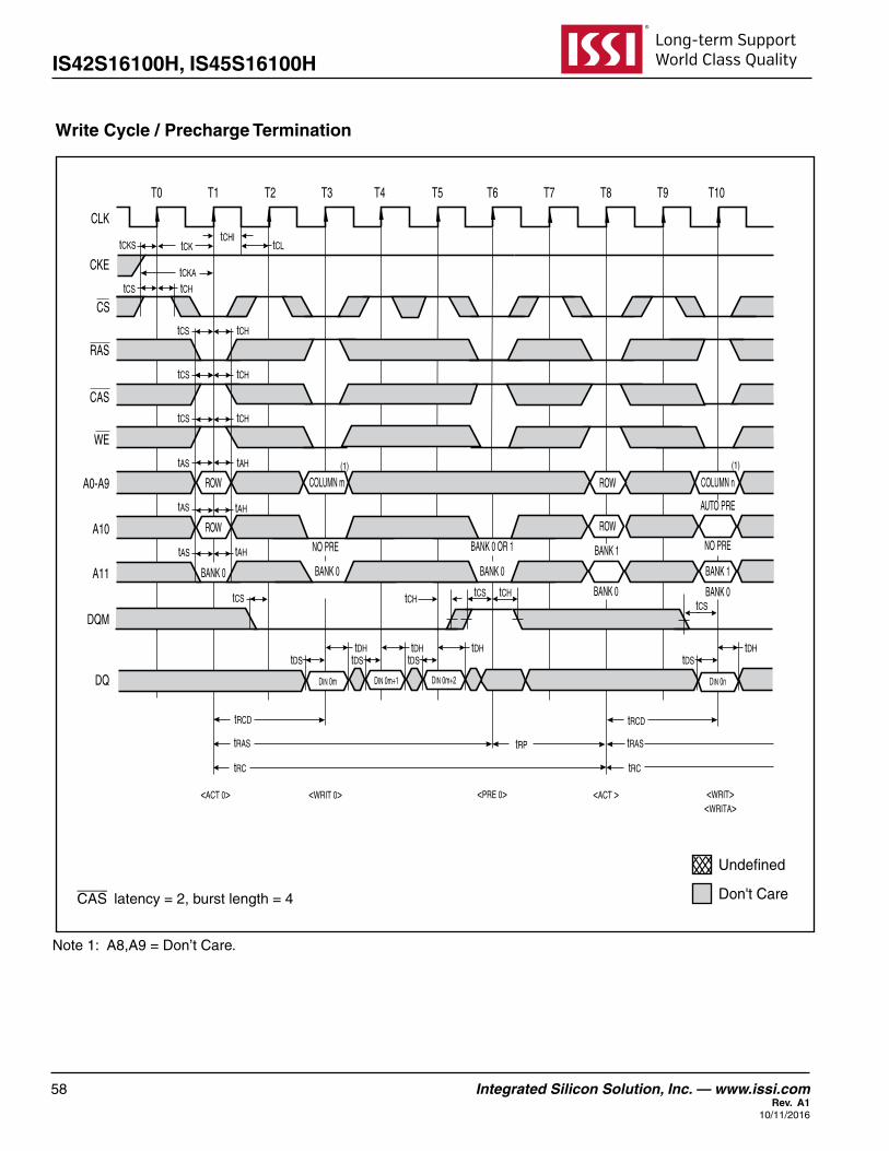
IS42S16100H, IS45S16100H
58 Integrated Silicon Solution, Inc. — www.issi.com Rev. A1
10/11/2016
Write Cycle / Precharge Termination
CLK
CKE
CS
RAS
CAS
WE
A0-A9
A10
A11
DQM
DQ
T0 T1 T2 T3 T4 T5 T6 T7 T8 T9 T10
tCKtCHI
tCL
tCHtCS
tCHtCS
tCHtCS
tCHtCS
tAHtAS
NO PRE
AUTO PRE
NO PREtAHtAS
tAHtAS
tCKS
tCKA
BANK 0 BANK 0
BANK 1
BANK 0 BANK 0
BANK 0
BANK 0 OR 1
ROW ROW
ROW
COLUMN m COLUMN n
ROW
tRAS
tRC tRC
<ACT 0> <ACT ><WRIT 0> <PRE 0> <WRIT><WRITA>
tRCD
tRP
tRCD
tRAS
BANK 1
DIN 0m DIN 0nDIN 0m+1 DIN 0m+2
tDStDStDStDStDHtDHtDHtDH
tCStCH tCStCS
tCH
(1) (1)
Don't Care
Undefined
CAS latency=2,burstlength=4
Note1:A8,A9=Don’tCare.

Integrated Silicon Solution, Inc. — www.issi.com 59Rev. A110/11/2016
IS42S16100H, IS45S16100H
Read Cycle / Byte Operation
CLK
CKE
CS
RAS
CAS
WE
A0-A9
A10
A11
LDQM
UDQM
DQ8-15
DQ0-7
T0 T1 T2 T3 T4 T5 T6 T7 T8 T9 T10
tCKtCHI
tCL
tCHtCS
tCHtCS
tCHtCS
tCHtCS
tAHtAS
BANK 1 BANK 1
BANK 0 AND 1
BANK 0 OR 1NO PRE
AUTO PRE
tCH
tAHtAS
tCS
tCS tCH
tAHtAS
tCKS
tCKA
BANK 0BANK 0
BANK 1
BANK 1
BANK 0 BANK 0
ROW COLUMN m
ROW
tQMD
tQMD
tRAS
tRC
<ACT> <ACT><READ><READA>
<MASKU> <MASKL><ENBU, MASKL> <PALL><PRE>
tRCD tCAC tQMD tRQL tRCD
tRAS
tRC
tRP
tAC tHZ
tOH
tAC tAC
tLZ
tLZ
tLZ
DOUT m
DOUT m
DOUT m+2
DOUT m+1
DOUT m+3
tOH
tOH
tOH
tACtAC
tOH
ROW
ROW
(1)
Don't Care
Undefined
CAS latency=2,burstlength=4
Note1:A8,A9=Don’tCare.

IS42S16100H, IS45S16100H
60 Integrated Silicon Solution, Inc. — www.issi.com Rev. A1
10/11/2016
Write Cycle / Byte Operation
CLK
CKE
CS
RAS
CAS
WE
A0-A9
A10
A11
LDQM
UDQM
DQ8-15
DQ0-7
T0 T1 T2 T3 T4 T5 T6 T7 T8 T9 T10
tCKtCHI
tCL
tCHtCS
tCHtCS
tCHtCS
tCHtCS
tAHtAS
BANK 1 BANK 1
BANK 0 AND 1
BANK 0 OR 1NO PRE
AUTO PRE
tCH
tAHtAS
tCS
tCS tCH
tAHtAS
tCKS
tCKA
BANK 0BANK 0
BANK 1
BANK 1
BANK 0 BANK 0
ROW COLUMN m
ROW
tRAS
tRC
<ACT> <ACT><WRIT><WRITA>
<MASK><MASKL> <ENB> <PALL><PRE>
tRCD tDPL tRCD
tRAS
tRC
tRP
ROW
ROW
tDH tDS tDS
tDH tDS
tDH tDS
DIN m
DIN m DIN m+3
tDH
tDH tDS
DIN m+1 DIN m+3
(1)
Don't Care
Undefined
CAS latency=2,burstlength=4
Note1:A8,A9=Don’tCare.

Integrated Silicon Solution, Inc. — www.issi.com 61Rev. A110/11/2016
IS42S16100H, IS45S16100H
Read Cycle, Write Cycle / Burst Read, Single Write
COLUMN n
CLK
CKE
CS
RAS
CAS
WE
A0-A9
A10
A11
DQM
DQ
T0 T1 T2 T3 T4 T5 T6 T7 T8 T9 T10
tCKtCHI
tCL
tCHtCS
tCHtCS
tCHtCS
tCHtCS
tAHtAS
BANK 1
BANK 0 AND 1
BANK 0 OR 1
NO PRE
NO PRE
AUTO PRE
tCH
tAHtAS
tCS
tAHtAS
tCKS
tCKA
BANK 0BANK 0
BANK 1
BANK 1
BANK 0
BANK 1
BANK 0
ROW COLUMN m
ROW
tQMD
tHZtLZ
tRAS
tRC
<ACT> <READ> <WRITA><WRIT>
<PALL><PRE>
tRCD tCAC tDPL
tRP
tAC tAC
tOH
tAC tAC
tOH tDH
tDS
tOH
DOUT m DOUT m+1 DOUT m+2
tOH
DOUT m+3 DIN n
(1) (1)
Don't Care
Undefined
CAS latency=2,burstlength=4
Note1:A8,A9=Don’tCare.

IS42S16100H, IS45S16100H
62 Integrated Silicon Solution, Inc. — www.issi.com Rev. A1
10/11/2016
Read Cycle
CLK
CKE
CS
RAS
CAS
WE
A0-A9
A10
A11
DQM
DQ
T0 T1 T2 T3 T4 T5 T6 T7 T8 T9 T10 T11 T12
tCKtCHI
tCL
tCHtCS
tCHtCS
tCHtCS
tCHtCS
tAHtAS
BANK 1
BANK 0 AND 1
BANK 0 OR 1
NO PRE
tAHtAS
tCS
tAHtAS
tCKS
tCKA
BANK 0BANK 0
BANK 1 BANK 1
BANK 0
BANK 1
BANK 0
ROW ROW
ROW
COLUMN m
ROW
tQMD
tLZ
tRAS
tRC
<ACT> <READ> <ACT><PRE><PALL>
tRCD tCAC tRQL
tRP
tRCD
tAC tAC
tOH
tAC tAC
tOH
tCH
tOH
DOUT m DOUT m+1 DOUT m+2
tOH
tHZ
DOUT m+3
tRC
tRAS
(1)
Don't Care
Undefined
CAS latency=3,burstlength=4
Note1:A8,A9=Don’tCare.

Integrated Silicon Solution, Inc. — www.issi.com 63Rev. A110/11/2016
IS42S16100H, IS45S16100H
Read Cycle / Auto-Precharge
CLK
CKE
CS
RAS
CAS
WE
A0-A9
A10
A11
DQM
DQ
T0 T1 T2 T3 T4 T5 T6 T7 T8 T9 T10 T11 T12
tCKtCHI
tCL
tCHtCS
tCHtCS
tCHtCS
tCHtCS
tAHtAS
BANK 1
AUTO PRE
tAHtAS
tCS
tAHtAS
tCKS
tCKA
BANK 0BANK 0
BANK 1 BANK 1
BANK 0
ROW
ROW
ROWCOLUMN
ROW
tQMD
tLZ
tRAS
tRC
<ACT> <READA> <ACT>
tRCD tCAC tPQL
tRP
tRCD
tAC tAC
tOH
tAC tAC
tOH
tCH
tOH
DOUT m DOUT m+1 DOUT m+2
tOH
tHZ
DOUT m+3
tRC
tRAS
(1)
CAS latency=3,burstlength=4
CLK
CKE
CS
RAS
CAS
WE
A0-A9
A10
A11
DQM
DQ
T0 T1 T2 T3 T4 T5 T6 T260 T261 T262 T263
tCKtCHI
tCL
tCHtCS
tCHtCS
tCHtCS
tCHtCS
tAHtAS
NO PREtAHtAS
tCS
tAHtAS
tCKS
tCKA
BANK 0BANK 0
BANK 0 OR 1
BANK 0
ROW COLUMN
ROW
tQMD
tLZ
tRAS
tRC(BANK 0)
<ACT 0> <READ0> <BST> <PRE 0>
tRCD tCAC(BANK 0)
tRBD
tAC tAC
tOH
tAC tAC tAC
tOH
tCH
tOH
DOUT 0m DOUT 0m+1 DOUT 0m-1
tOH
tHZ
tOH
DOUT 0m DOUT 0m+1
tRP(BANK 0)
(1)
Undefined
Note1:A8,A9=Don’tCare.

IS42S16100H, IS45S16100H
64 Integrated Silicon Solution, Inc. — www.issi.com Rev. A1
10/11/2016
Read Cycle / Full Page
CLK
CKE
CS
RAS
CAS
WE
A0-A9
A10
A11
DQM
DQ
T0 T1 T2 T3 T4 T5 T6 T7 T8 T262 T263 T264 T265
tCKtCHI
tCL
tCHtCS
tCHtCS
tCHtCS
tCHtCS
tAHtAS
NO PRE
tAHtAS
tCS
tAHtAS
tCKS
tCKA
BANK 0BANK 0
BANK 0 OR 1
BANK 0
ROW COLUMN
ROW
tLZ
tRAS(BANK 0)
tRC(BANK 0)
<ACT 0> <READ0> <BST> <PRE 0>
tRCD(BANK 0)
tCAC(BANK 0)
tRBD
tAC tAC
tOH
tAC tAC tAC
tOH
tCH
tOH
DOUT 0m DOUT 0m+1 DOUT 0m-1
tOH
tHZ
tOH
DOUT 0m DOUT 0m+1
tRP(BANK 0)
(1)
CAS latency=3,burstlength=fullpage Don't Care
Undefined
Note1:A8,A9=Don’tCare.

Integrated Silicon Solution, Inc. — www.issi.com 65Rev. A110/11/2016
IS42S16100H, IS45S16100H
Read Cycle / Ping Pong Operation (Bank Switching)
CLK
CKE
CS
RAS
CAS
WE
A0-A9
A10
A11
DQM
DQ
T0 T1 T2 T3 T4 T5 T6 T7 T8 T9 T10 T11 T12
tCKtCHI
tCL
tCHtCS
tCHtCS
tCHtCS
tCHtCS
tAHtAS
BANK 0 BANK 1 BANK 0 BANK1 BANK 0BANK 1BANK 0
BANK 0 OR 1 BANK 0 OR 1NO PRE NO PRE
tCH
tAHtAS
tQMDtCS
tAC tAC tAC tAC
tRCD(BANK 0)
tRAS(BANK 0)
<ACT 0><ACT 0> <ACT1> <READ 0><READA 0> <READA 1>
<READ 1> <PRE 0> <PRE 1>
tAHtAS
tCKS
tCKA
ROW ROW
ROW ROW
ROWCOLUMN COLUMN
AUTO PRE AUTO PRE
ROW
tLZ
tRAS(BANK 1)
tRC(BANK 1)
tRCD(BANK 1)
tCAC(BANK 1)
tCAC(BANK 0)
tRC(BANK 0)
tRQL(BANK 0)
tRP(BANK 0)
tRCD(BANK 0)
tRAS(BANK 0)
tRP(BANK1)
tRC(BANK 0)
tRRD(BANK 0 TO 1)
tOH tOH tOH tOH
tHZ
DOUT 0m DOUT 0m+1 DOUT 1m DOUT 1m+1
(1) (1)
CAS latency=3,burstlength=2 Don't Care
Undefined
Note1:A8,A9=Don’tCare.

IS42S16100H, IS45S16100H
66 Integrated Silicon Solution, Inc. — www.issi.com Rev. A1
10/11/2016
Write Cycle
CLK
CKE
CS
RAS
CAS
WE
A0-A9
A10
A11
DQM
DQ
T0 T1 T2 T3 T4 T5 T7 T6 T8 T9 T10 T11
tCKtCHI
tCL
tCHtCS
tCHtCS
tCHtCS
tCHtCS
tAHtAS
BANK 1
BANK 0
BANK 0 OR 1
BANK 0 AND 1
NO PRE
tCH
tAHtAS
tCS
tDS tDS tDS tDStDH
tRAS
tRC
<PRE><PALL>
<ACT><ACT> <WRIT>
tAHtAS
tCKS
tCKA
ROW ROW
ROW
COLUMN
ROW
tRCD
tDH tDH tDH
tRP
tDPL tRCD
tRAS
tRC
DIN m DIN m+2DIN m+1 DIN m+3
BANK 1
BANK 0
BANK 1
BANK 0
BANK 1
BANK 0
T12
(1)
CAS latency=3,burstlength=4 Don't Care
Undefined
Note1:A8,A9=Don’tCare.

Integrated Silicon Solution, Inc. — www.issi.com 67Rev. A110/11/2016
IS42S16100H, IS45S16100H
Write Cycle / Auto-Precharge
CLK
CKE
CS
RAS
CAS
WE
A0-A9
A10
A11
DQM
DQ
T0 T1 T2 T3 T4 T5 T7 T6 T8 T9 T10
tCKtCHI
tCL
tCHtCS
tCHtCS
tCHtCS
tCHtCS
tAHtAS
BANK 1
BANK 0
AUTO PRE
tCH
tAHtAS
tCS
tDS tDS tDS tDStDH
tRAS
tRC
<ACT><ACT> <WRITA>
tAHtAS
tCKS
tCKA
ROW ROW
ROW
COLUMN
ROW
tRCD
tDH tDH tDH
tRP
tDAL tRCD
tRAS
tRC
DIN m DIN m+2DIN m+1 DIN m+3
BANK 1
BANK 0
BANK 1
BANK 0
T11 T12
(1)
CAS latency=3,burstlength=4 Don't Care
Undefined
Note1:A8,A9=Don’tCare.

IS42S16100H, IS45S16100H
68 Integrated Silicon Solution, Inc. — www.issi.com Rev. A1
10/11/2016
Write Cycle / Full Page
CLK
CKE
CS
RAS
CAS
WE
A0-A9
A10
A11
DQM
DQ
T0 T1 T2 T3 T4 T5 T259T6 T260 T261 T262 T263 T264
tCKtCHI
tCL
tCHtCS
tCHtCS
tCHtCS
tCHtCS
tAHtAS
NO PRE
tAHtAS
tCS
tAHtAS
tCKS
tCKA
BANK 0BANK 0
BANK 0 OR 1
BANK 0
ROW COLUMN
ROW
tRAS
tRC
<ACT 0> <WRIT0> <BST> <PRE 0>
tRCD
tCH
tDPL
tRP
tDS tDS tDS tDStDH tDH tDH tDH
DIN 0m DIN 0m+2DIN 0m+1 DIN 0m-1 DIN 0m
(1)
CAS latency=3,burstlength=fullpage Don't Care
Undefined
Note1:A8,A9=Don’tCare.

Integrated Silicon Solution, Inc. — www.issi.com 69Rev. A110/11/2016
IS42S16100H, IS45S16100H
Write Cycle / Ping-Pong Operation (Bank Switching)
CLK
CKE
CS
RAS
CAS
WE
A0-A9
A10
A11
DQM
DQ
T0 T1 T2 T3 T4 T5 T6 T7 T8 T9 T10
tCKtCHI
tCL
tCHtCS
tCHtCS
tCHtCS
tCHtCS
tAHtAS
BANK 0 BANK 0 BANK 0BANK 1BANK 1
BANK 0 OR 1NO PRE NO PRE
tCH
tAHtAS
tCS
tDS tDS
tRCD(BANK 0)
tRAS(BANK 0)
<ACT 0> <ACT 1> <WRIT 0><WRITA 0> <WRITA 1>
<WRIT 1> <PRE 0> <ACT 0>
tAHtAS
tCKS
tCKA
ROW ROW
ROW
ROW
ROW
COLUMN COLUMN
AUTO PREAUTO PRE
ROW
tRCD(BANK 1)
tRAS(BANK 1)
tRC(BANK 1)
tRC(BANK 0)
tRCD
tRP(BANK 0)
tRAS
tRC
tRRD(BANK 0 TO 1)
tDPL(BANK 0)
tDPL
tDH tDH tDS tDH tDH
DIN 0m
tDS tDS tDH tDS tDH tDH tDHtDS tDS
DIN 0m+1 DIN 0m+2 DIN 0m+3 DIN 1m DIN 1m+1 DIN 1m+2 DIN 1m+3
T11 T12
BANK 0
BANK 1
(1) (1)
CAS latency=3,burstlength=4 Don't Care
Undefined
Note1:A8,A9=Don’tCare.

IS42S16100H, IS45S16100H
70 Integrated Silicon Solution, Inc. — www.issi.com Rev. A1
10/11/2016
Read Cycle / Page Mode
CLK
CKE
CS
RAS
CAS
WE
A0-A9
A10
A11
DQM
DQ
T0 T1 T2 T3 T4 T5 T6 T7 T8 T9 T10
tCKtCHI
tCL
tCHtCS
tCHtCS
tCHtCS
tCHtCS
tAHtAS
BANK 1 BANK 0 BANK 0 BANK 0 BANK 0
BANK 1
BANK 0 OR 1
BANK 0 AND 1
BANK 1
tCH
tAHtAS
tLZ
tCS
tRAS
tRC
<ACT> <READ><READA><READ><READ>
<PALL><PRE>
tAHtAS
tCKS
tCKA
ROW COLUMN m COLUMN n COLUMN o
NO PRE NO PRE
NO PRE
AUTO PRE
ROW
tRCD tCACtCAC
tCAC
tRQL
tHZ
tRP
tQMD
BANK 1
BANK 0 BANK 1
tAC tAC
tOH
tAC tAC tAC tAC
tOH tOH tOH tOH tOH
DOUT m DOUT m+1 DOUT n DOUT n+1 DOUT o DOUT o+1
T11 T12
(1) (1)(1)
CAS latency=3,burstlength=2Don't Care
Undefined
Note1:A8,A9=Don’tCare.

Integrated Silicon Solution, Inc. — www.issi.com 71Rev. A110/11/2016
IS42S16100H, IS45S16100H
Read Cycle / Page Mode; Data Masking
CAS latency=3,burstlength=2
CLK
CKE
CS
RAS
CAS
WE
A0-A9
A10
A11
DQM
DQ
T0 T1 T2 T3 T4 T5 T6 T7 T8 T9 T10
tCKtCHI
tCL
tCHtCS
tCHtCS
tCHtCS
tCHtCS
tAHtAS
BANK 1
BANK 0 BANK 0 BANK 0 BANK 0BANK 1
BANK 0 OR 1
BANK 0 AND 1
BANK 1
tQMD
tAHtAS
tLZ
tCS
tRAS
tRC
<ACT> <READ> <READ> <ENB><READA, MASK><READ, MASK>
<PALL><PRE>
tAHtAS
tCKS
tCKA
ROW COLUMN m COLUMN n COLUMN o
NO PRE NO PRENO PRE
AUTO PRE
ROW
tCH
tRCD tCACtCAC
tCAC
tRQL
tHZ
tRP
tQMD
BANK 1
BANK 0
BANK 1
tAC tAC
tOH
tAC tAC tAC
tOH tOH tOH tOH
DOUT m DOUT m+1 DOUT n DOUT o DOUT o+1
T11 T12
(1) (1) (1)
Don't Care
Undefined
Note1:A8,A9=Don’tCare.

IS42S16100H, IS45S16100H
72 Integrated Silicon Solution, Inc. — www.issi.com Rev. A1
10/11/2016
Write Cycle / Page Mode
CAS latency=3,burstlength=2
CLK
CKE
CS
RAS
CAS
WE
A0-A9
A10
A11
DQM
DQ
T0 T1 T2 T3 T4 T5 T6 T7 T8 T9 T10
tCKtCHI
tCL
tCHtCS
tCHtCS
tCHtCS
tCHtCS
tAHtAS
BANK 0
BANK 0 BANK 0 BANK 0BANK 1
BANK 0 OR 1
BANK 0 AND 1
BANK 1
tCH
tAHtAS
tCS
tRAS
tRC
<ACT> <WRIT><WRITA><WRIT><WRIT> <MASK>
<PALL><PRE>
tAHtAS
tCKS
tCKA
ROW COLUMN m COLUMN n COLUMN o
NO PRE NO PRENO PRE
AUTO PRE
ROW
tRCD tDPL
tRP
BANK 1
BANK 0
BANK 1
tDS tDS tDStDH tDStDH tDH tDH tDS tDH
DIN m DIN nDIN m+1 DIN o DIN o+1
T11 T12
(1) (1) (1)
Don't Care
Undefined
Note1:A8,A9=Don’tCare.

Integrated Silicon Solution, Inc. — www.issi.com 73Rev. A110/11/2016
IS42S16100H, IS45S16100H
Write Cycle / Page Mode; Data Masking
CAS latency=3,burstlength=2
CLK
CKE
CS
RAS
CAS
WE
A0-A9
A10
A11
DQM
DQ
T0 T1 T2 T3 T4 T5 T6 T7 T8 T9 T10 T11 T12
tCKtCHI
tCL
tCHtCS
tCHtCS
tCHtCS
tCHtCS
tAHtAS
BANK 1
BANK 0 BANK 0 BANK 0 BANK 0BANK 1
BANK 1OR 0
BANK 0 AND 1
BANK 1
tCH
tAHtAS
tCS
tRAS
tRC
<ACT> <WRIT> <WRIT><WRITA><WRIT><MASK>
<PALL><PRE>
tAHtAS
tCKS
tCKA
ROW COLUMN m COLUMN n COLUMN o
NO PRE NO PRENO PRE
AUTO PRE
ROW
tRCD tDPL
tRP
BANK 1
BANK 0
BANK 1
tDS tDS tDStDH tDStDH tDH tDH tDS tDH
DIN m DIN nDIN m+1 DIN o DIN o+1
(1) (1) (1)
Don't Care
Undefined
Note1:A8,A9=Don’tCare.

IS42S16100H, IS45S16100H
74 Integrated Silicon Solution, Inc. — www.issi.com Rev. A1
10/11/2016
Read Cycle / Clock Suspend
CAS latency=3,burstlength=2
CLK
CKE
CS
RAS
CAS
WE
A0-A9
A10
A11
DQM
DQ
T0 T1 T2 T3 T4 T5 T6 T7 T8 T9 T10 T11
tCKtCHI
tCL
tCHtCS
tCHtCS
tCHtCS
tCHtCS
tAHtAS
NO PRE
AUTO PRE
tAHtAS
tCS
tCKH
tAHtAS
tCKS
tCKA
tCKS
BANK 1BANK 0 BANK 0
BANK 1
BANK 0
BANK 0 AND 1
BANK 0 OR 1
ROW COLUMN m
ROW
tQMD
tLZ
tRAS
tRC
<ACT> <READ><READ A>
<SPND> <SPND> <PRE><PALL>
tRCD tCAC
tAC tAC
tOH tOH
tCH
DOUT m DOUT m+1
tHZ
tRP
T12
BANK 1
(1)
Don't Care
Undefined
Note1:A8,A9=Don’tCare.

Integrated Silicon Solution, Inc. — www.issi.com 75Rev. A110/11/2016
IS42S16100H, IS45S16100H
Write Cycle / Clock Suspend
CAS latency=3,burstlength=2
CLK
CKE
CS
RAS
CAS
WE
A0-A9
A10
A11
DQM
DQ
T0 T1 T2 T3 T4 T5 T6 T7 T8 T9 T10
tCKtCHI
tCL
tCHtCS
tCHtCS
tCHtCS
tCHtCS
tAHtAS
NO PRE
AUTO PRE
tAHtAS
tCS
tCKH
tAHtAS
tCKS
tCKA
tCKS
BANK 1BANK 0
BANK 1
BANK 1
BANK 0 BANK 0
BANK 1
BANK 0
BANK 0 AND 1
BANK 0 OR 1
ROW ROW
ROW
COLUMN m
ROW
tDS
tRAS
tRC tRC
<ACT> <ACT ><WRIT, SPND><WRITA, SPND>
<SPND> <PRE><PALL>
tRCD
tCH
tDH tDH tDS
tDPL
tRP tRAS
DIN m DIN m+1
T11 T12
(1)
Don't Care
Undefined
Note1:A8,A9=Don’tCare.

IS42S16100H, IS45S16100H
76 Integrated Silicon Solution, Inc. — www.issi.com Rev. A1
10/11/2016
Read Cycle / Precharge Termination
CAS latency=3,burstlength=2
CLK
CKE
CS
RAS
CAS
WE
A0-A9
A10
A11
DQM
DQ
T0 T1 T2 T3 T4 T5 T6 T7 T8 T9 T10
tCKtCHI
tCL
tCHtCS
tCHtCS
tCHtCS
tCHtCS
tAHtAS
NO PREtAHtAS
tCS
tAHtAS
tCKS
tCKA
BANK 0
BANK 0
BANK 0
ROW ROW
ROW
COLUMN m
ROW
tQMD
tLZ
tRAS
tRC tRP
<ACT 0> <ACT><READ 0> <PRE 0>
tRCD tCAC tRQL
tRP
tRCD
tAC tAC
tOH
tAC tHZ
tOH tOH
tCH
DOUT m DOUT m+2
tRAS
BANK 1
DOUT m+1
T11 T12
BANK 0
BANK 0 OR 1
(1)
Don't Care
Undefined
Note1:A8,A9=Don’tCare.

Integrated Silicon Solution, Inc. — www.issi.com 77Rev. A110/11/2016
IS42S16100H, IS45S16100H
Write Cycle / Precharge Termination
CAS latency=3,burstlength=4
CLK
CKE
CS
RAS
CAS
WE
A0-A9
A10
A11
DQM
DQ
T0 T1 T2 T3 T4 T5 T6 T7 T8 T9 T10
tCKtCHI
tCL
tCHtCS
tCHtCS
tCHtCS
tCHtCS
tAHtAS
NO PREtAHtAS
tAHtAS
tCKS
tCKA
BANK 0
BANK 0
BANK 0
ROW ROW
ROW
COLUMN m
ROW
tRC tRP
<ACT 0> <ACT ><WRIT 0> <PRE 0>
tRCD
tRP
tRCD
tRAS
BANK 1
DIN 0m DIN 0m+1 DIN 0m+2
tDStDStDStDHtDHtDH
T11 T12
tCH tCHtCS tCS
BANK 0
BANK 0 OR 1
tRAS
(1)
Don't Care
Undefined
Note1:A8,A9=Don’tCare.

IS42S16100H, IS45S16100H
78 Integrated Silicon Solution, Inc. — www.issi.com Rev. A1
10/11/2016
Read Cycle / Byte Operation
CAS latency=3,burstlength=4
CLK
CKE
CS
RAS
CAS
WE
A0-A9
A10
A11
LDQM
UDQM
DQ8-15
DQ0-7
T0 T1 T2 T3 T4 T5 T6 T7 T8 T9 T10 T11
tCKtCHI
tCL
tCHtCS
tCHtCS
tCHtCS
tCHtCS
tAHtAS
BANK 1 BANK 1
BANK 0 AND 1
BANK 0 OR 1NO PRE
AUTO PRE
tCH
tAHtAS
tCS
tCS tCH
tAHtAS
tCKS
tCKA
BANK 0BANK 0
BANK 1
BANK 1
BANK 0 BANK 0
ROW COLUMN m
ROW
tQMD
tQMD
tRAS
tRC
<ACT> <ACT><READ><READA>
<MASKU> <MASKL><ENBU, MASKL> <PALL><PRE>
tRCD tCAC tQMD tRQL tRCD
tRAS
tRP
tRP
tAC tHZ
tOH
tHZ
tHZ
tAC tAC
tLZ
tLZ
tLZ
DOUT m
DOUT m
DOUT m+2
DOUT m+1
DOUT m+3
tOH
tOH
tACtAC
tOH
ROW
ROW
T12
(1)
Don't Care
Undefined
Note1:A8,A9=Don’tCare.

Integrated Silicon Solution, Inc. — www.issi.com 79Rev. A110/11/2016
IS42S16100H, IS45S16100H
Write Cycle / Byte Operation
CAS latency=3,burstlength=4
CLK
CKE
CS
RAS
CAS
WE
A0-A9
A10
A11
LDQM
UDQM
DQ8-15
DQ0-7
T0 T1 T2 T3 T4 T5 T6 T7 T8 T9 T10
tCKtCHI
tCL
tCHtCS
tCHtCS
tCHtCS
tCHtCS
tAHtAS
BANK 1 BANK 1
BANK 0 AND 1
BANK 0 OR 1NO PRE
AUTO PRE
tCH
tAHtAS
tCS
tCS tCH
tAHtAS
tCKS
tCKA
BANK 0BANK 0
BANK 1
BANK 1
BANK 0 BANK 0
ROW COLUMN m
ROW
tRAS
tRC
<ACT> <ACT><WRIT><WRITA>
<MASK><MASKL> <ENB> <PALL><PRE>
tRCD tDPL tRCD
tRAStRP
tRP
ROW
ROW
tDH tDS tDS
tDH tDS
tDH tDS
DIN m
DIN m DIN m+3
tDH
tDH tDS
DIN m+1 DIN m+3
T12T11
(1)
Don't Care
Undefined
Note1:A8,A9=Don’tCare.

IS42S16100H, IS45S16100H
80 Integrated Silicon Solution, Inc. — www.issi.com Rev. A1
10/11/2016
Read Cycle, Write Cycle / Burst Read, Single Write
CAS latency=3,burstlength=2
COLUMN n
CLK
CKE
CS
RAS
CAS
WE
A0-A9
A10
A11
DQM
DQ
T0 T1 T2 T3 T4 T5 T6 T7 T8 T9 T10
tCKtCHI
tCL
tCHtCS
tCHtCS
tCHtCS
tCHtCS
tAHtAS
BANK 1
BANK 0 AND 1
BANK 0 OR 1
NO PRE
NO PRE
AUTO PRE
tCH
tAHtAS
tCS
tAHtAS
tCKS
tCKA
BANK 0BANK 0
BANK 1
BANK 1
BANK 0
BANK 1
BANK 0
ROW COLUMN m
ROW
tQMD
tHZtLZ
tRAS
tRC
<ACT> <READ> <WRITA><WRIT>
<PALL><PRE>
tRC tCAC tDPL
tRP
tACtAC
tDH
tDS
tOH
DOUT m
tOH
DOUT m+1 DIN n
T11 T12
(1) (1)
Don't Care
Undefined
Note1:A8,A9=Don’tCare.

Integrated Silicon Solution, Inc. — www.issi.com 81Rev. A110/11/2016
IS42S16100H, IS45S16100H
Frequency Speed (ns) Order Part No. Package166 MHz 6 IS45S16100H-6TLA1
IS45S16100H-6BLAI
400-mil TSop II, Lead-free
143MHz 7 IS45S16100H-7TLA1 400-mil TSop II, Lead-free IS45S16100H-7BLA1 60-ball Bga, Lead-free
Frequency Speed (ns) Order Part No. Package143MHz 7 IS45S16100H-7TLA2 400-mil TSop II, Lead-free
IS45S16100H-7BLA2 60-ball Bga, Lead-free
Frequency Speed (ns) Order Part No. Package166 MHz 6 IS42S16100H-6TLI 400-mil TSop II, Lead-free
IS42S16100H-6BLI 60-ball Bga, Lead-free143MHz IS42S16100H-7TLI 400-mil TSop II, Lead-free
IS42S16100H-7BLI 60-ball Bga, Lead-free
please contact ISSI for leaded parts support.
ORDERING INFORMATIONCommercial Range: 0°C to 70°C
Industrial Range: -40°C to +85°C
Automotive Range: -40°C to +85°C
Automotive Range: -40°C to +105°C
Frequency Speed (ns) Order Part No. Package200 MHz 5 IS42S16100H-5T 400-mil TSop II
IS42S16100H-5TL 400-mil TSop II, Lead-freeIS42S16100H-5BL 60-ball Bga, Lead-free
166 MHz 6 IS42S16100H-6T 400-mil TSop IIIS42S16100H-6TL 400-mil TSop II, Lead-freeIS42S16100H-6BL 60-ball Bga, Lead-free
143MHz 7 IS42S16100H-7T 400-mil TSop IIIS42S16100H-7TL 400-mil TSop II, Lead-freeIS42S16100H-7BL 60-ball Bga, Lead-free

IS42S16100H, IS45S16100H
82 Integrated Silicon Solution, Inc. — www.issi.com Rev. A1
10/11/2016
No
Te :
Θ
Θ4. form
ed leads shall be planar with respect to one another w
ithin 0.1mm
3. d
imension b does not include dam
bar protrusion/intrusion.
1. controlling dim
ension : mm
at the seating plane after final test.
2. dim
ension d and e1 do not include m
old protrusion .
09/01/2006Package O
utline

Integrated Silicon Solution, Inc. — www.issi.com 83Rev. A110/11/2016
IS42S16100H, IS45S16100H