introduction to the stanford nanofabrication facility and ... · introduction to the stanford...
TRANSCRIPT

Introduction to the Stanford Nanofabrication Facility and Research Examples
presented to the IEEE Santa Clara Valley Solid State Circuits SocietyJanuary 19, 2006
Paul Rissman, Director of Research [email protected]

2
Agenda
• location of the Stanford Nanofabrication Facility• NNIN – National Nanotechnology Infrastructure Network• overview of SNF
– vision, mission, strategy– organization– equipment resources
• research examples (primarily from Stanford)– nanotubes, nanowires– optical devices– silicon based devices– new semiconductor materials– fundamental physics– MEMs/NEMs– magnetic devices– miscellaneous
• success stories• finances

3

4
The National Nanotechnology Infrastructure Network (NNIN)
http://www.nnin.org
The SNF is a member of the NNIN, an integrated partnership of thirteen university user facilities, supported in part by National Science Foundation.
• University of California at Santa Barbara• Cornell University • Georgia Institute of Technology • Harvard University• Howard University• University of Michigan• University of Minnesota• University of New Mexico• North Carolina State University• Penn State• Stanford University• University of Texas at Austin • University of Washington
members of original NNUN

5
To enable rapid advancements in science, engineering and technology down to the nano-scale by efficient access to nanotechnology infrastructure.
NNIN Vision and Mission

6
NNIN Strategy
• comprehensive science and engineering resources for the nanoscale.
• expertise, processes, and process support – not just equipment.
• on-site and remote use.• an integrated national resource through the web infrastructure.• distributed technical specialization and complex integration
resources.• geographically distributed sites.• external user-focussed commitment backed by strong internal
strength.
to provide:

7
Stanford Nanofabrication Facility Vision
To be one of the top fabrication infrastructures for nanotechnology research and education in the world measured in terms of quality and quantity of work in nanotechnology.
Raith 150 electron beam system
SVG develop track

8
SNF Mission
To provide an environment in which users can try innovative ideas for scientific research, engineering research, and development of innovative products.
To provide a fabrication infrastructure which helps both academic and industrial users accomplish their experimental research goals.
SVG resist coat track
Lam TCP 9400 poly etch system
9
SNF Strategy
• to provide user operated experimental capabilities with advanced equipment and effective training in order to maintain a safe working environment.
• to acquire, in a timely manner, necessary equipment and process capabilities.
• to balance the budget with NSF/NNIN funding and user fees while establishing a process for new equipment acquisition.
• to enable close coupling and information exchange between academic and industrial users.
• to strengthen resources as necessary in order to meet the demand for new technical knowledge and new skills.
• to increase the use of nanofabrication in non-traditional areas.• to provide an incubator facility for start-up companies.

10
The Nanofab’s Philosophy
• the lab is open to all – Stanford academic, non-Stanford academic and industrial users.
• there is a dynamic community of researchers who support one another. There is an active problem discussion list.
• there are consultants who work with users that don’t want to come to Stanford to get their project done in the lab.
• each user is responsible for his or her own intellectual property.
• it is a cost effective and efficient way to try out new ideas.
• by terms of the NSF agreement only R&D can be done, no manufacturing.
Tylan furnace
Zygo optical profilometer
User’s Perspective on SNF’s Value
• the SNF plays a vital role in the incubation of new technologies– most foundries have $50k+ barrier to entry - access gap– flexibility to try non-conventional processes– variety of equipment– hands-on opportunities appealing to Ph.D. founder types– home turf advantage to [Stanford] grads– SNF’s secret weapon: today’s academic users are tomorrow’s
industrial users• excellent work environment
– friendly and knowledgeable staff– supportive learning environment– collegial atmosphere– most users are good citizens
Dr. Alissa FitzgeraldA. M. Fitzgerald & Associates, LLC655 Skyway Rd., Suite 118, San Carlos, CA 94070www.amfitzgerald.com
12
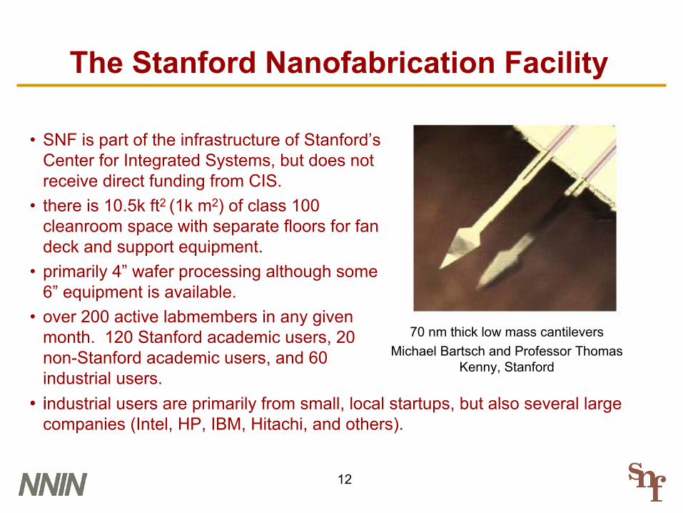
• industrial users are primarily from small, local startups, but also several large companies (Intel, HP, IBM, Hitachi, and others).
The Stanford Nanofabrication Facility
• SNF is part of the infrastructure of Stanford’s Center for Integrated Systems, but does not receive direct funding from CIS.
• there is 10.5k ft2 (1k m2) of class 100 cleanroom space with separate floors for fan deck and support equipment.
• primarily 4” wafer processing although some 6” equipment is available.
• over 200 active labmembers in any given month. 120 Stanford academic users, 20 non-Stanford academic users, and 60 industrial users.
• i
70 nm thick low mass cantileversMichael Bartsch and Professor Thomas
Kenny, Stanford

CIS Member Companies• Advanced Micro Devices• Agilent Technologies• Analog Devices• Applied Materials• Canon• Ebara Corporation• Hewlett-Packard Company• Hitachi Ltd• IBM Corporation• Infineon• Intel Corporation• LG Electronics, Inc.• National Semiconductor Corporation• Panasonic
• Philips• Renesas Technology Corporation• Robert Bosch Corporation• Texas Instruments, Incorporated• Toshiba• TSMC

14
SNF Organization
Prof. Yoshio Nishi
Paul Rissmanstrategic issues
budgetadministration
Mary Tangbiotech liaison
processing/trainingoutreach(7 staff)
Dick Craneequip maint
facility safetycode compliance
(8 staff)
Cam Chanmonthly accounting
NSF contractbusiness development
Ed Myersprocess development
new materialsnew equipmentcontamination
John ShottNNIN liaison
CORAL developmentERT
labmember services(3 staff)
Jim McVittie/Mike Deallab consultants
special programs
total lab headcount - 25

15
• remote users program • symposia and workshops• CIS new user grants program (for
Stanford and non-Stanford faculty)
• summer research internships for undergraduate students and high school teachers
• participation in educational curriculum development
• social and ethical issues in nanotechnology
Special Programs
pillar transistor – Teresa Kramer and Professor Fabian Pease,
Stanford

16
Interdisciplinary Workshops/Symposia
• BioMEMS• E-Beam Lithography for Nanostructure
Fabrication• Biomedical Applications of
Nanofabrication• DNA Microarray Workshop • Plasma Etching Workshop• Nanosafety - Dec. 2, 2004 at Georgia
Tech• Foundry Day – Prototype to Product –
October 20, 2005 at Stanford
carbon nanotubes

17
Stanford Nanocharacterization Laboratory (SNL)contacts – Ann Marshall, Richard Chin, Professor Robert Sinclair
• associated with SNF through NNIN grant• high resolution scanning electron
microscopes (SEM)• focussed ion beam (FIB)• high resolution transmission electron
microscope (TEM) • high resolution Auger electron
spectroscopy (AES)• x-ray photoelectron spectroscopy (XPS)• secondary ion mass spectroscopy (SIMS)• specimen preparation equipment• x-ray diffraction laboratory
nanowires – Professor Yoshio Nishi and H. Jagannathan, Stanford
SSI S-Probe monochromatizedXPS spectrometer

18
electronics14%
optics14%
materials6%
physics11%
chemistry5%
life sciences7%
process research
11%
MEMs/NEMs/mech engr
32%
Areas of Research at SNF
data for calendar year 2004

19
• Hitachi HL 700F direct-write electron beam system.
– medium throughput– resolution limited to ~150 nm
• Raith direct-write electron beam system.– low throughput– high resolution down to 10 nm
E-Beam Lithography Resources
Raith resolution test pattern
9 nm holes imaged on Raith
20
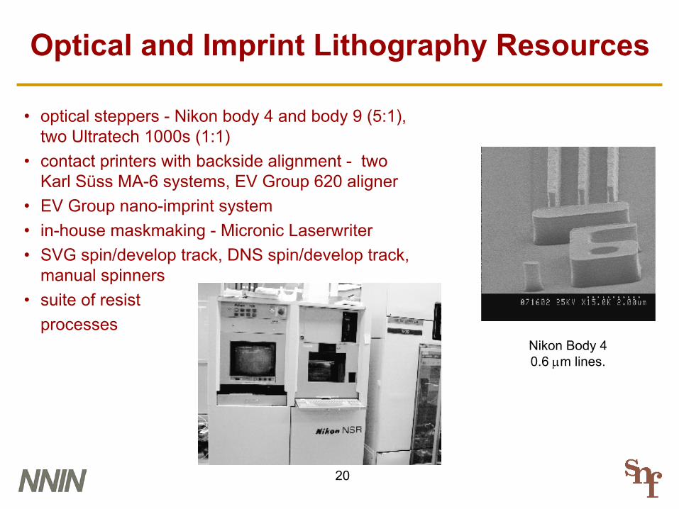
• optical steppers - Nikon body 4 and body 9 (5:1), two Ultratech 1000s (1:1)
• contact printers with backside alignment - two Karl Süss MA-6 systems, EV Group 620 aligner
• EV Group nano-imprint system• in-house maskmaking - Micronic Laserwriter• SVG spin/develop track, DNS spin/develop track,
manual spinners• suite of resist
processes
Optical and Imprint Lithography Resources
Nikon Body 4 0.6 µm lines.

21
Etch Resources
• deep silicon etch – two STS Multiplex ICP reactive ion etch systems.
• silicon/poly etch - Lam Research TCP 9400.
• nitride/oxide/silicon/polymer etch – Applied Materials 8100.
• metals/oxide/nitride/silicon/resist strip -Applied Materials 5000 cluster tool.
• GaAs/films etch – PlasmaQuest ECR etcher.
• miscellaneous materials – three Drytek 100 etchers.
• resist strip – Matrix and Gasonics
spring transducerKlaasen, et al., Stanford
STS etcher

22
Thin Films Resources
• gate oxide growth• LPCVD of poly, nitride, • low temperature oxide• low-stress nitride• low stress PECVD of dielectrics• ASM Epsilon II single wafer
epitaxial reactor - silicon, silicon/germanium, germanium
• atomic layer deposition system –Al2O3
• metal sputtering and evaporation -Cu, Al, AlSi, W, Ti, Au, Cr, Pt, NiCr
• sputtering of some dielectrics and ferromagnetic materials
535nm
48nm
high aspect ratio nitride spacerHoon Cho and Professor Krishna Saraswat, Stanford

23
Analytical Tools
• scanning electron microscopes Hitachi S-800 – out of fabHitachi 4160 – in fab
• Digital Instruments atomic force microscope
• Zygo optical profilometer• ellipsometer, profilometers• spectrophotometer• resistivity mapping• film stress gauge
3-D cell network substrate and microelectrode arrayRainer Fasching, Kyle Hammerick, Eric Tao,
Professor Fritz Prinz, Stanford

24
Miscellaneous Equipment
• wafer aligner/bonder - EV Group, Karl Süss
• Tousimis critical point dryer• HF vapor etch• thermal bonding• wafer saw• chemical mechanical polishing
for dielectric materials
flow channel system cross section (top) and injector needle (bottom)Stefan Zappe, John Zhang and
Professor Olav Solgaard, Stanford
GlassSilicon Glass
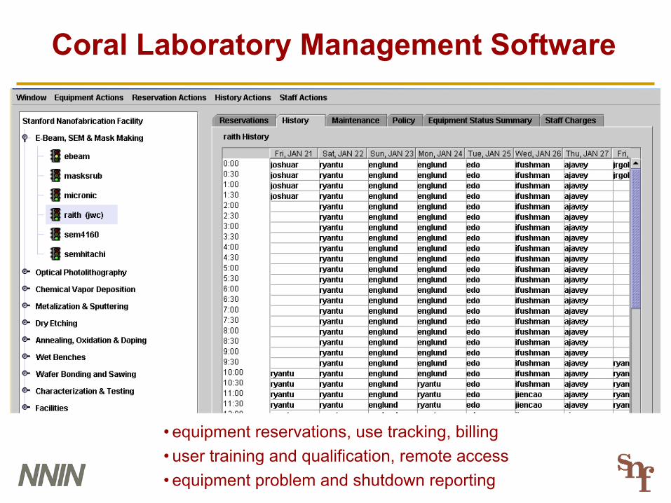
Coral Laboratory Management Software
• equipment reservations, use tracking, billing• user training and qualification, remote access• equipment problem and shutdown reporting