introduction to microfabrication - mcgill physicspeter/534a/vengallatore2.pdf · introduction to...
TRANSCRIPT

1
PHYS 534 (Fall 2008)
Lecture 2
Introduction to Microfabrication
1Srikar Vengallatore, McGill University
How are Microsystems Designed?
Market need
C tEvaluationCreativity
Concept
Embodiment
D t il
of competitiony
& experience
Modeling andAnalysis
Manufacturingconsiderations
In house Management
2
Product Specification
DetailIn-house expertise
Managementdecisions
2
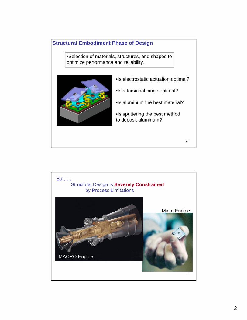
Structural Embodiment Phase of Design
•Selection of materials, structures, and shapes to optimize performance and reliability.
•Is electrostatic actuation optimal?
•Is a torsional hinge optimal?
•Is aluminum the best material?
3
•Is sputtering the best methodto deposit aluminum?
But,….Structural Design is Severely Constrained
by Process Limitations
Micro Engine
4
MACRO Engine
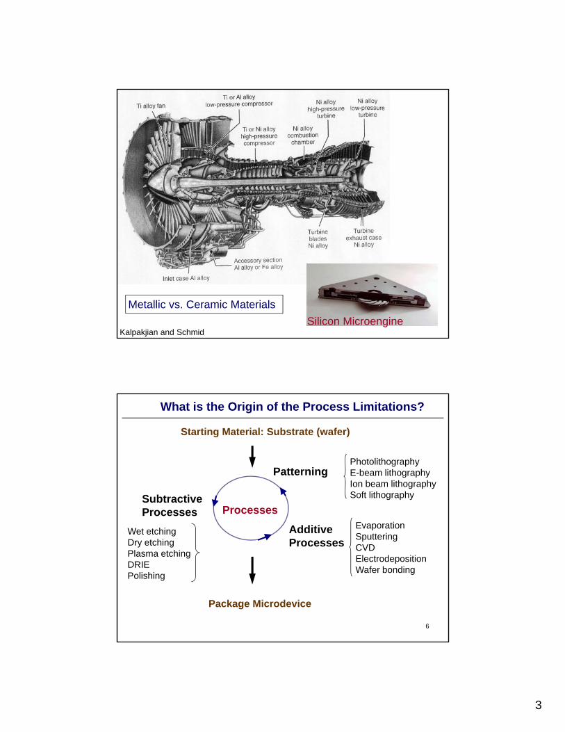
3
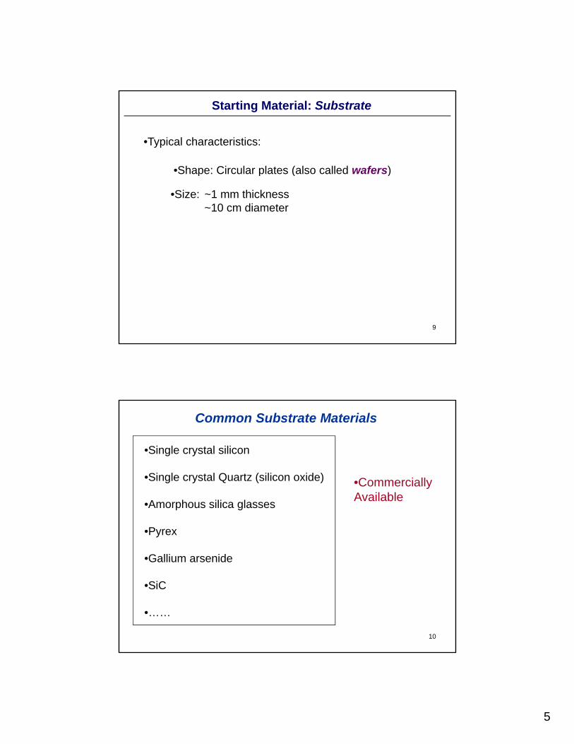
5Kalpakjian and Schmid
Silicon MicroengineMetallic vs. Ceramic Materials
Patterning
Starting Material: Substrate (wafer)
What is the Origin of the Process Limitations?
PhotolithographyE-beam lithography
Processes
g
Additive Processes
SubtractiveProcesses
EvaporationSputteringCVDElectrodeposition
g p yIon beam lithographySoft lithography
Wet etchingDry etchingPlasma etching
6
Package Microdevice
ElectrodepositionWafer bondingDRIE
Polishing

4
Microfabrication differs from macro-machining in several ways:
•Material removal is by selective corrosion
•Structural thin films are not available from a catalog.I t d h t t th fil b f h i itInstead, we have to create the film before shaping it
•Defining a pattern follows a process that resemblesPhotography (of the old-fashioned type using photosensitivefilms)
7
•Massively parallel manufacture
•Simultaneous manufacture and assembly
Catalog of Manufacturing Processes
Patterning Techniques: Photolithography, Microstamping,Electron/ion beam lithography,Soft lithography,…
Additive processes: Thin-film deposition, wafer bonding,oxidation, epitaxy, …..
Subtractive processes: Wet etching, dry etching, ion milling,
8
p g, y g, g,deep reactive ion etching,…
5
Starting Material: Substrate
•Typical characteristics:
•Shape: Circular plates (also called wafers)p p ( )
•Size: ~1 mm thickness~10 cm diameter
9
Common Substrate Materials
•Single crystal silicon
•Single crystal Quartz (silicon oxide) •Commercially
•Amorphous silica glasses
•Pyrex
•Gallium arsenide
CommerciallyAvailable
10
•SiC
•……
6
How are Silicon Wafers Specified?
Chemistry: Purity; Dopant concentration
Electrical Properties: Resistivity
Geometry: Diameter;
Thickness;
Total thickness variations;
Surface finish and polish;
B d
11Virginia Semiconductor (http://www.virginiasemi.com/) and many others
Bow and warpage;
Crystallographic Orientation;
Primary & secondary flats
Specification of Chemistry
Impurities: Carbon, oxygen, heavy metals,…
Typically, O2: 5 – 25 ppmC: 1 5 ppmC: 1 – 5 ppmMetals: < 1 ppb
Some impurities are intentionally added in small,well-defined, quantities
12
e de ed, qua es
Such impurities are called DOPANTS
7
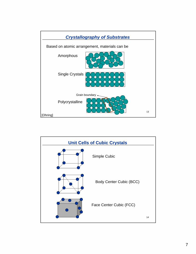
Crystallography of Substrates
Based on atomic arrangement, materials can be
Amorphous
Single Crystals
13
Polycrystalline
Grain boundary
[Ohring]
Unit Cells of Cubic Crystals
Simple Cubic
Body Center Cubic (BCC)
14
Face Center Cubic (FCC)
8
Directions of a Cubic Crystals
z [0,0,1]
y
Unit Distance
[0,1,0]
[1,0,1]
15
x [1,0,0]
[1,1,0]
Miller indices of Crystal Planes
[0,0,1]
[1,0,0]
[0,1,0]
Recipe: 1. Determine intercepts on each axis 1, 1, ∞
16
2. Take reciprocals of these numbers 1, 1, 0
3. Reduce to smallest integers (110)
9
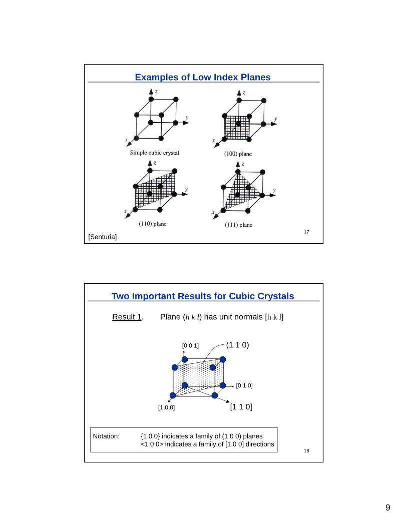
Examples of Low Index Planes
17[Senturia]
Two Important Results for Cubic Crystals
Result 1. Plane (h k l) has unit normals [h k l]
(1 1 0)
[0,1,0]
[0,0,1] (1 1 0)
18
[1,0,0] [1 1 0]
Notation: {1 0 0} indicates a family of (1 0 0) planes<1 0 0> indicates a family of [1 0 0] directions

10
Two Important Results for Cubic Crystals
Result 2. The angle (γ) between two planes with indices(h1 k1 l1) and (h2 k2 l2) is given by
22
22
22
21
21
21
212121coslkhlkh
llkkhh++++
++=γ
Example: (i) The angle between (100) and (111) is
19
011 7.543
1cos31001cos ==⎥⎦
⎤⎢⎣
⎡ ++= −−γ
Crystallography of Single-Crystal Silicon Wafers
Look for the primary flat
(111) Wafers
(100) Wafers
20[Maluf]

11
Representation of a Simple Process Flow
1 mm
10 cm
21
Golden Rule of Process Representation:
NOTHING is EVER drawn to scale!
Thin-Film Deposition
1 mm
Thin Film
22
Thin Film1 μm
12
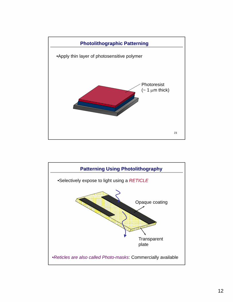
Photolithographic Patterning
•Apply thin layer of photosensitive polymer
Photoresist(~ 1 μm thick)
23
•Selectively expose to light using a RETICLE
Patterning Using Photolithography
Opaque coating
24
Transparent plate
•Reticles are also called Photo-masks: Commercially available
13
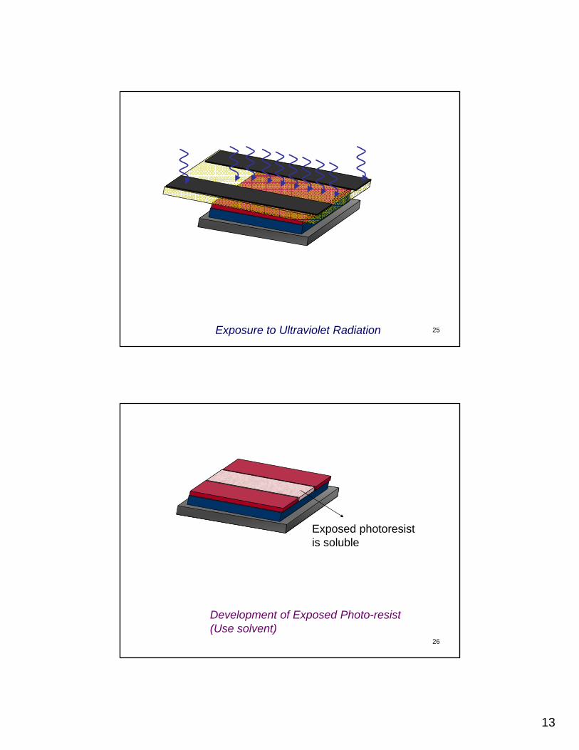
25Exposure to Ultraviolet Radiation
Exposed photoresistis soluble
26
Development of Exposed Photo-resist(Use solvent)
14
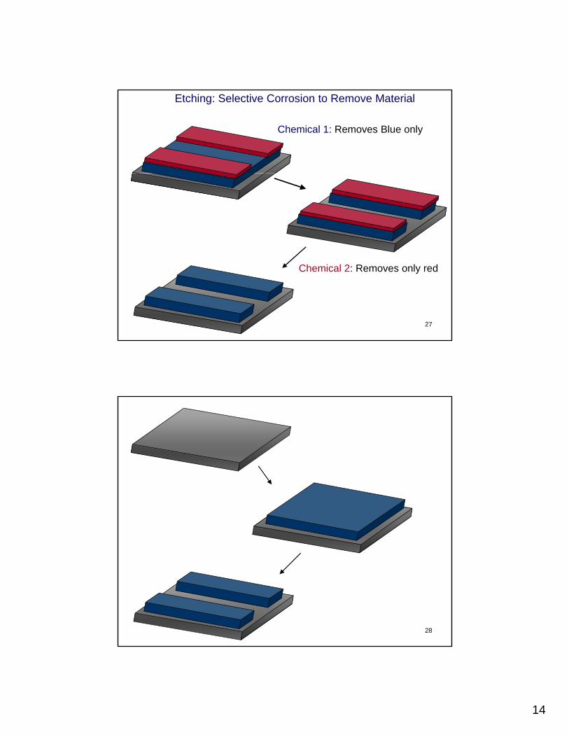
Etching: Selective Corrosion to Remove Material
Chemical 1: Removes Blue only
27
Chemical 2: Removes only red
28

15
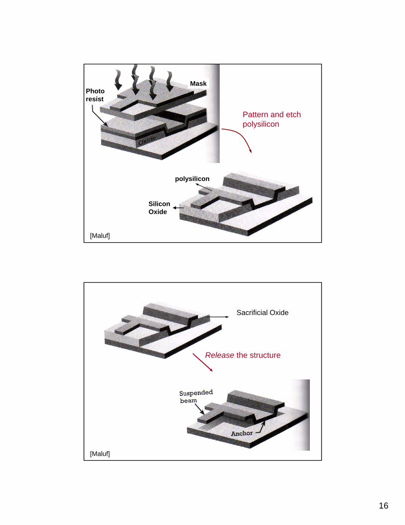
Next: A Surface-Micromachining Process..
•Addition, Patterning & Selective Removal of Thin Films
Silicon Oxide
29[Maluf]
Silicon
Silicon oxide
Deposit polysilicon thin film
30
16
Pattern and etchpolysilicon
Photoresist
Mask
polysilicon
polysilicon
31
SiliconOxide
[Maluf]
Sacrificial Oxide
Release the structure
32[Maluf]

17
2-d Representation of Process Flows
33
Again, Not to Scale!
2-d Representation of Process Flow(Photolithographic details not shown)
34Substrate Silicon Oxide Polysilicon
18
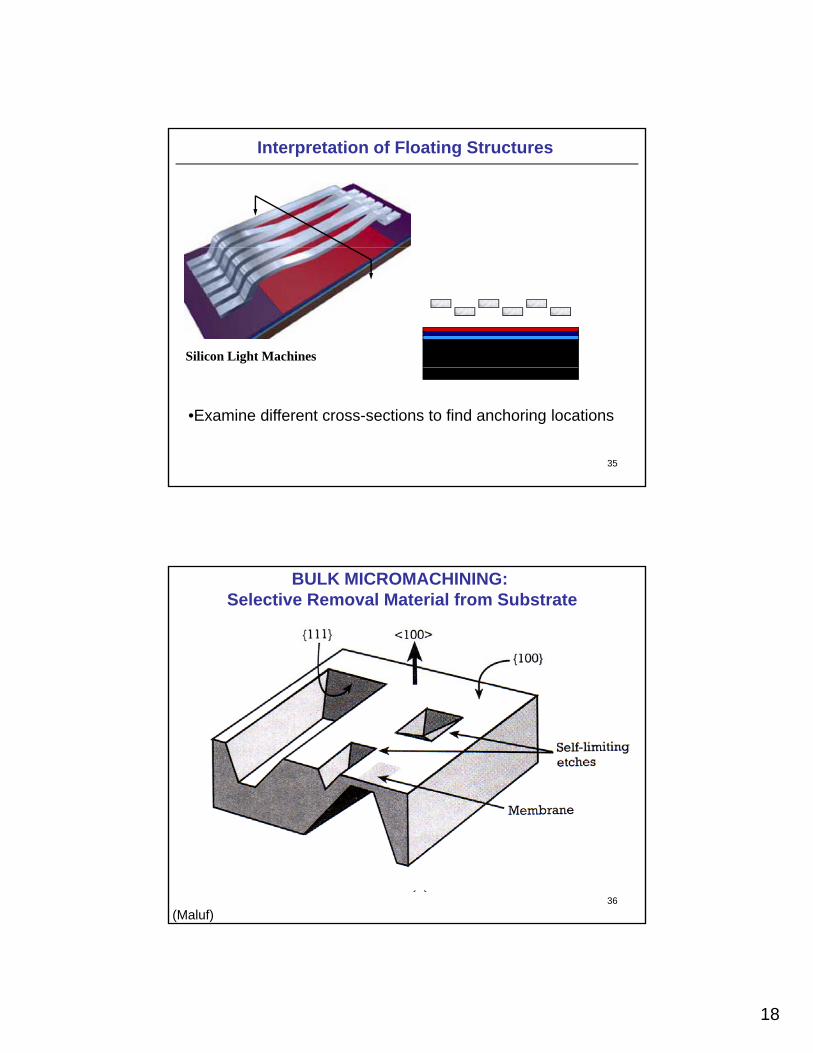
Interpretation of Floating Structures
Silicon Light Machines
35
•Examine different cross-sections to find anchoring locations
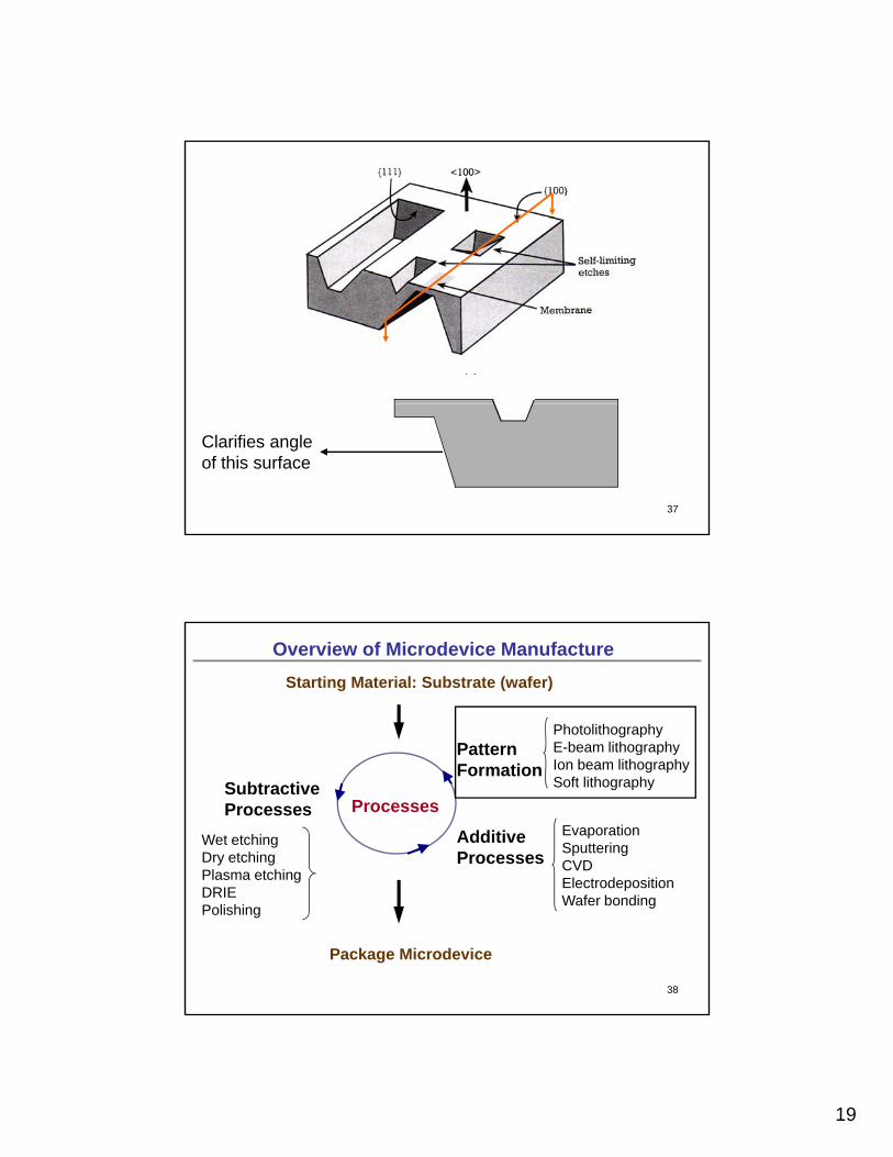
BULK MICROMACHINING: Selective Removal Material from Substrate
36(Maluf)
19
37
Clarifies angleof this surface
Pattern
Starting Material: Substrate (wafer)
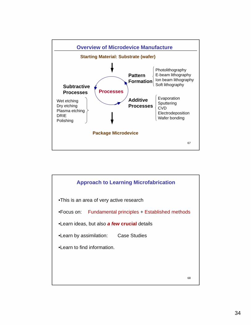
Overview of Microdevice Manufacture
PhotolithographyE-beam lithography
Processes
Pattern Formation
Additive Processes
SubtractiveProcesses
EvaporationSputteringCVDElectrodeposition
g p yIon beam lithographySoft lithography
Wet etchingDry etchingPlasma etching
38
Package Microdevice
ElectrodepositionWafer bondingDRIE
Polishing
20
Lithos: Stone graphy: to write
Photolithography: Pattern transfer using photons
H d S f UV di ti ( li )Hardware: Source of UV radiation (aligner)
Reticle (master pattern)
Photoresist (polymer)
Chemical solvents
39
Chemical solvents
Basic Steps in Photolithography
CoatPhotoresist
Expose toUltraviolet radiation
Develop
40
mask
21
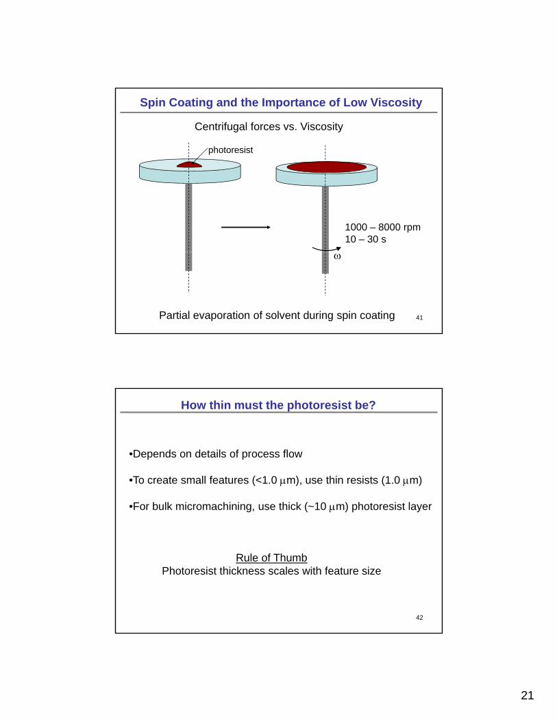
Spin Coating and the Importance of Low Viscosity
Centrifugal forces vs. Viscosity
photoresist
1000 – 8000 rpm10 – 30 s
41
ω
Partial evaporation of solvent during spin coating
How thin must the photoresist be?
•Depends on details of process flow
•To create small features (<1.0 μm), use thin resists (1.0 μm)
•For bulk micromachining, use thick (~10 μm) photoresist layer
42
Rule of ThumbPhotoresist thickness scales with feature size

22
Two Types of Photoresists
Exposed regions become soluble
Exposed regionsbecome insoluble
43POSITIVE resist NEGATIVE resist
Mechanisms linked to Bond Formation/Destruction
Before Exposure
After Exposure
44Positive Resist Negative Resist

23
Examples of Positive & Negative Resists
Positive: PMMA (poly methyl methacrylate)
DQN (diaquinone ester + phenolic novolak)DQN (diaquinone ester + phenolic novolak)
Negative: bis(aryl)azide rubber resists
45
•Photoresists are commercially available
[Madou]
Photolithographic Aligners
Source of Radiation
Focusing optics
Tooling for Alignment
46[Senturia]

24
ALIGNER
http://www.physics.mcgill.ca/nanotools/
ALIGNER
47
Pattern
Starting Material: Substrate (wafer)
Overview of Microdevice Manufacture
PhotolithographyE-beam lithography
Processes
Pattern Formation
Additive Processes
SubtractiveProcesses
EvaporationSputteringCVDElectrodeposition
g p yIon beam lithographySoft lithography
Wet etchingDry etchingPlasma etching
48
Package Microdevice
ElectrodepositionWafer bondingDRIE
Polishing
25
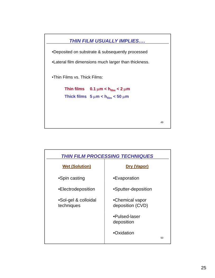
THIN FILM USUALLY IMPLIES….
•Deposited on substrate & subsequently processed
•Lateral film dimensions much larger than thickness.
•Thin Films vs. Thick Films:
Thin films 0.1 μm < hfilm < 2 μm
Thick films 5 μm < hfil < 50 μm
49
Thick films 5 μm < hfilm < 50 μm
THIN FILM PROCESSING TECHNIQUES
Wet (Solution) Dry (Vapor)
•Spin casting •Evaporation
•Electrodeposition
•Sol-gel & colloidaltechniques
•Sputter-deposition
•Chemical vapor deposition (CVD)
50
•Pulsed-laser deposition
•Oxidation
26
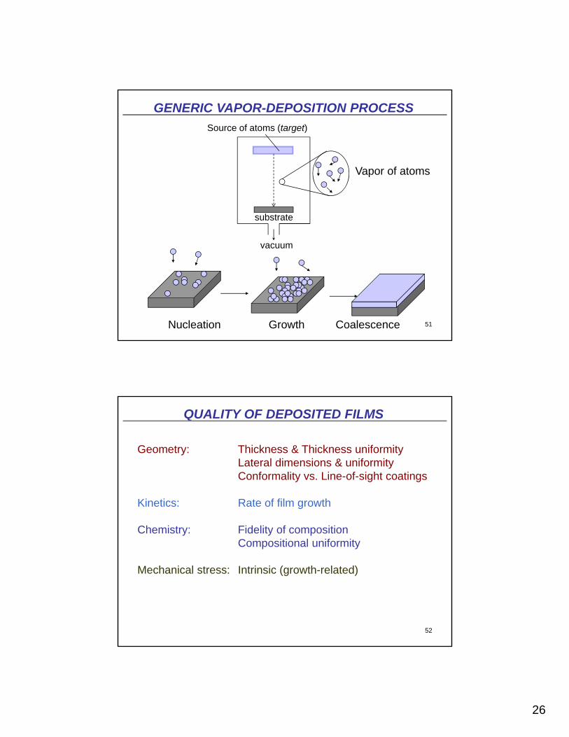
GENERIC VAPOR-DEPOSITION PROCESSSource of atoms (target)
Vapor of atoms
vacuum
substrate
Vapor of atoms
51Nucleation Growth Coalescence
QUALITY OF DEPOSITED FILMS
Geometry: Thickness & Thickness uniformityLateral dimensions & uniformityConformality vs. Line-of-sight coatingsConformality vs. Line of sight coatings
Kinetics: Rate of film growth
Chemistry: Fidelity of compositionCompositional uniformity
52
Mechanical stress: Intrinsic (growth-related)
27
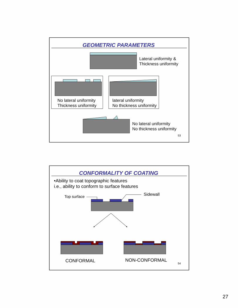
GEOMETRIC PARAMETERS
Lateral uniformity &Thickness uniformity
No lateral uniformityThickness uniformity
lateral uniformityNo thickness uniformity
53
y y
No lateral uniformityNo thickness uniformity
CONFORMALITY OF COATING•Ability to coat topographic featuresi.e., ability to conform to surface features
Top surface Sidewall
54CONFORMAL NON-CONFORMAL

28
Material Addition Using Wafer Bonding
Wafer 1
•Direct Wafer Bonding
Wafer 2
•Intermediate Wafer Bonding
55Metal; Glass; Oxide; Polymer
High Strength Bonding is Possible(Bonded regions as strong as lattice!)
56
29
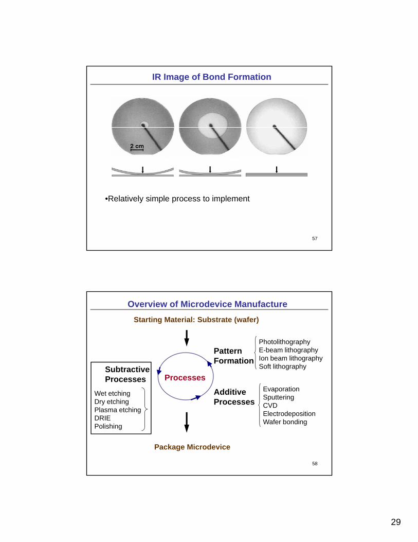
IR Image of Bond Formation
57
•Relatively simple process to implement
Pattern
Starting Material: Substrate (wafer)
Overview of Microdevice Manufacture
PhotolithographyE-beam lithography
Processes
Pattern Formation
Additive Processes
SubtractiveProcesses
EvaporationSputteringCVDElectrodeposition
g p yIon beam lithographySoft lithography
Wet etchingDry etchingPlasma etching
58
Package Microdevice
ElectrodepositionWafer bondingDRIE
Polishing

30
Example 1: Development of Photoresist (Wet Etching)
Key Concept: Material Removal by Chemical Corrosion
Exposed photoresist
59
Exposed photoresistis soluble
How to Design a Etch Process
•What etchants (chemicals/plasma) should I use?
H l ill th t k (i KINETICS)?•How long will the process take (i.e., KINETICS)?
I th t h ISOTROPIC ANISOTROPIC?
•Is the etch SELECTIVE?(i.e., what materials can I work on?)
60
•How do I detect completion of etch process?(i.e., END – POINT DETECTION)
•Is the etch ISOTROPIC or ANISOTROPIC?(i.e., what SHAPES can I make?)
31
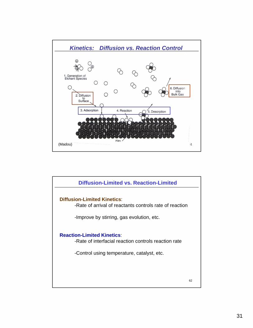
Kinetics: Diffusion vs. Reaction Control
61(Madou)
Diffusion-Limited vs. Reaction-Limited
Diffusion-Limited Kinetics:-Rate of arrival of reactants controls rate of reaction
-Improve by stirring, gas evolution, etc.
Reaction-Limited Kinetics:-Rate of interfacial reaction controls reaction rate
62
-Control using temperature, catalyst, etc.
32
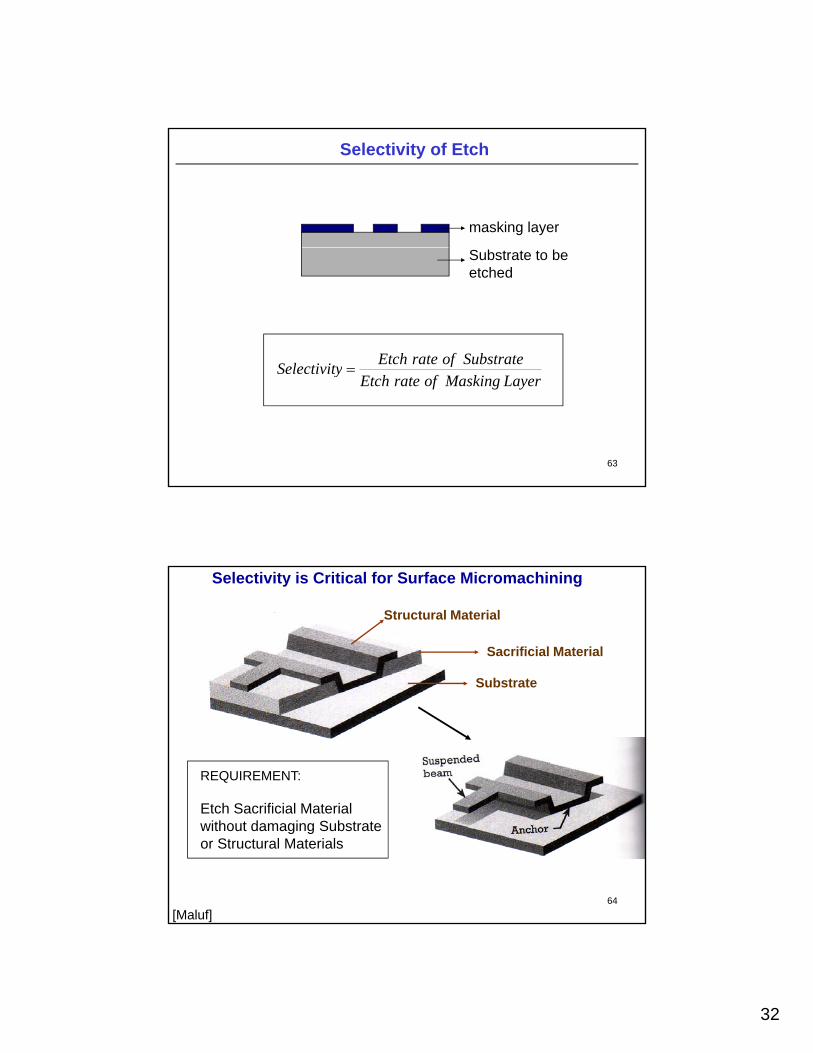
Selectivity of Etch
masking layer
Substrate to be etched
SubstrateofrateEtchySelectivit
63
LayerMaskingofrateEtchfySelectivit =
Sacrificial Material
Substrate
Structural Material
Selectivity is Critical for Surface Micromachining
Substrate
REQUIREMENT:
Et h S ifi i l M t i l
64
Etch Sacrificial Materialwithout damaging Substrateor Structural Materials
[Maluf]

33
Isotropic vs. Anisotropic Etches
Isotropic
65AnisotropicEtch front
Gases and Plasma are also used for Etching
•Vapor Phase Dry Etching (non-plasma)
•Plasma-assisted Dry Etching
-Ion Milling (Focused Ion-Beam Milling)
-Ashing
66
-Reactive-Ion Etching
-Deep Reactive-Ion Etching
34
Pattern
Starting Material: Substrate (wafer)
Overview of Microdevice Manufacture
PhotolithographyE-beam lithography
Processes
Pattern Formation
Additive Processes
SubtractiveProcesses
EvaporationSputteringCVDElectrodeposition
g p yIon beam lithographySoft lithography
Wet etchingDry etchingPlasma etching
67
Package Microdevice
ElectrodepositionWafer bondingDRIE
Polishing
Approach to Learning Microfabrication
•This is an area of very active research
•Focus on: Fundamental principles + Established methods•Focus on: Fundamental principles + Established methods
•Learn ideas, but also a few crucial details
•Learn by assimilation: Case Studies
•Learn to find information
68
Learn to find information.