glass microfabrication and other microfabrication...
TRANSCRIPT
�������������
�����������������������������
������������������
������������������������������������������������������������
���������
�����������������������������������������������
�������������
�����������������������������
������������������
������������������������������������������������������������
���������
�����������������������������������������������

2. Glass microfabrication andTopics in this lectureother microfabrication techniquesGlass and other less
established materials inmicrofabricationChoice of materialsubstrates are particular " Introductioninteresting from theapplication point of view inchemistry and " Strategic developments:biochemistry. Besidesplastics, glass is the most - Utilizing microelectronic techniquespopular of all materials inLab-on-a-Chip for non-silicon materials.'microfluidic' devices.
" Tackling glass integration.The MEMS tricksSame concepts other " Other materials and diversity ofgoals
techniques.Structural elementsFrom design to device- how " Outlook: Future developmentsto select the appropriatetechnique?
Summary
Monday, August, 15, 2005 Regina Luttge
Topics in this section
Glass as materialaFabrication principles
I! Pcceeu,ieej a rracrure
rage particle cite:
3 .30 micrer
80 230 'co-c
~~T-r'e'
Introduction
" Glass micromachining:- Material preparation,- Established patterning techniques,- Specially developed techniques for
fast, through-wafer structuring in
glass and other brittle materials.
" Miscellaneous used techniques inmicrofluidics.
Monday, August, 15, 2005 Regina Luttge
2.1. Introduction
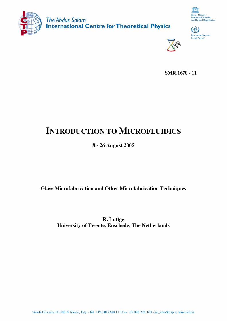
Why glass?
Bulk and thin-film processing in glass popular due to
generally chemical inertness of the material andexisting record of glass surface chemistry.
N1/4icromachining based on developments insemiconductor microelectronic industry where glass isused as:- as an electrical isolation material,- as chemical inert material (capping),- as material with low interference (electromagnetic waves,
acoustic pick up),-
Monday, August, 15, 2005 Regina Lutge
2.1. Introduction
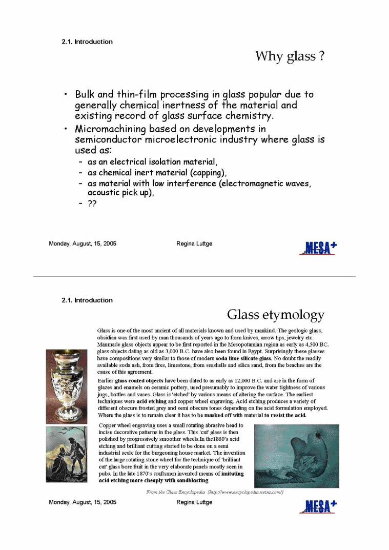
Glass etymologyGlass is one ofthe most ancient of all materials known and used by mankind. The geologic glass,obsidian was first used by man thousands ofyears ago to form knives, arrow tips, jewelry etc.Manmade glass objects appear to be first reported in the Mesopotamian region as early as 4,500 BC.
glass objects dating as old as 3,000 B.C. have also been found in Egypt. Surprisingly these glasseshave compositions very similar to those of modem soda lime silicate glass. No doubt the readilyavailable soda ash, from fires, limestone, from seashells and silica sand, from the beaches are thecause of this agreement.Earlier glass coated objects have been dated to as early as 12,000 B.C. and are in the form of
glazes and enamels on ceramic pottery, used presumably to improve the water tightness ofvarious
jugs, bottles and vases. Glass is 'etched' by various means of altering the surface. The earliesttechniques were acid etching and copper wheel engraving. Acid etching produces a variety ofdifferent obscure frosted grey and semi obscure tones depending on the acid formulation employed.Where the glass is 10 remain clear it has to be masked offwith material to resist the acid.
Copper wheel engraving uses a small rotating abrasive head toincise decorative patterns in the glass. This 'cur glass is then
polished by progressively smoother wheels.In the1860's acid
etching and brilliant cutting started to be done on a semiindustrial scale for the burgeoning house market. The inventionofthe large rotating stone wheel for the technique of'brilliant,.. frcut' glass bore fruit in the very elaborate panels mostly seen inpubs. In the late 1870's craftsmen invented means of imitating t
'--
acid etchingmore cheaply with sandblasting p -£k, Glass E'wydopstha {?rtprtsnw.snsyclsps'tha.ssrsz.csmIJ
Monday, August, 15, 2005 Regina Lutge +
2.1. Introduction
Glass: the material
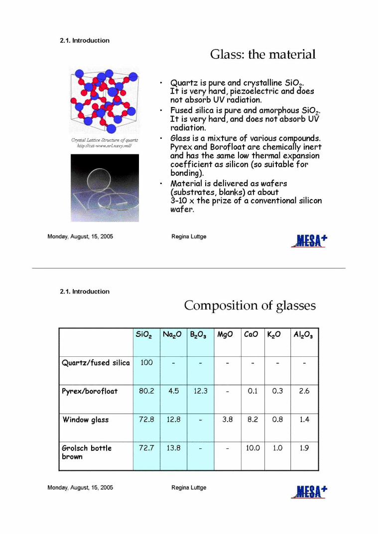
" Quartz is pure and crystalline 5i02.It is very hard, piezoelectric and doesnot absorb UV radiation.
" Fused silica is pure and amorphous 5i02.It is very hard, and does not absorb UVradiation.
C,ystalLaWceZtructur¬cfqz4csnz Glass is a mixture of various compounds.Pyrex and Borofloat are chemically inertand has the same low thermal expansioncoefficient as silicon (so suitable forbonding).
I Material is delivered as wafers-
(substrates, blanks) at aboutI 3-lOx the prize of a conventional silicon
Monday, August, 15, 2005 Regina Lutge _1IESA
2.1. Introduction
Composition of glasses
5i02 Na20 B203 M90 CaO K20 A1203
Quartz/fused silica 100 - - - - - -
Pyrex/borofloat 80.2 4.5 12.3 - 0.1 0.3 2.6
Window glass 72.8 12.8 - 3.8 8.2 0.8 1.4
&rolsch bottlebrown
72.7 13.8 - - 10.0 1.0 1.9
Monday, August, 15, 2005 Regina Lutge JIESA

2.1. Introduction
Float glass manufactureEstablished industrial process for many glass types
From window glass and other household appliances to
high tech applications.
"Floating glass, melt"Vloeibaaiglas
Monday, August, 15, 2005 Regina Luttge
2.1. Introduction
Floatglass quality
The good and the bad side of float glass
AFM of chemicalmechanical polishing (CAAP)
of the float side
roughness: 0.23 nm roughness: 4.2 nm
roughness: 0.49 nm
J. W van uwkaene. Unnrs4y oj7Sventn, 2004, u'ubizshed
Monday, August, 15, 2005 Regina Lutge
Lipsceeri Toprollers Tinbad"Slit inlet""Upper "Tin bath"
transport roles" Giasrechmek3 2002
AFM of top side IAFM of float side
2.1. Introduction
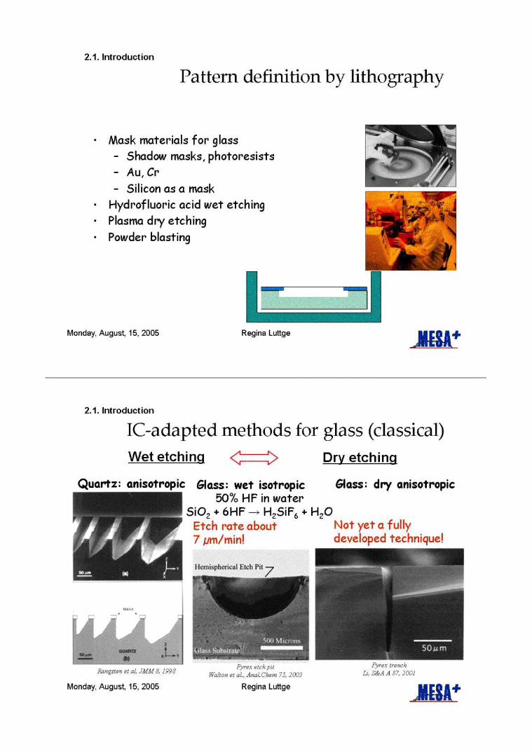
Pattern definition by lithography
" Mask materials for glass- Shadow masks, photoresists- Au, Cr- Silicon as a mask
" Hydrofluoric acid wet etching" Plasma dry etching" Powder blasting
Monday, August, 15, 2005
2.1. Introduction
IC-adapted methods for glass (classical)Wet etching Dry etching
4 At
L.a!. .-AIM 3. ms's
Monday, August, 15, 2005
Glass: wet isotropic Glass: dry anisotropic50% HF in water
5i02 + 6HF
H2SiF6+ H20Etch rate about Not yet a fully7 gm/minideveloped technique!
Hemispherical Etch Pit
rwTt U'r---
£vraa nch wca a!.. Anal.Chn1 75. 205'S
Regina Lutge
--r1 __
Regina Lutge JIESAt
Quartz: anisotropic
2&.4A 27,20')!
Topics in this section
Glass microfluidic chipfabrication&integration
Monday, August, 15, 2005
Strategic developments
" Glass microfludic chip fabricationtechniques
" From MEMS to spin-offs" Selection of fabrication techniques is
based on pattern feasibility and criticaldimensions in the design- Choice of material often restricts the
fabrication technique used.- Critical dimensions often restrict the
material-fabrication combinations tochoose from.
Regina Luttge
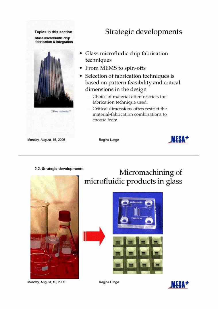
2.2. Strategic developments
Micromachining ofmicrofluidic products in glass
I.1jItJ
a
II =U S
S
m u
Regina Lutge
"Ljtcss catwara1
Monday, August, 15, 2005

2.2. Strategic developments
Wet-chemically etched channels
f:4Irttl:IhtIt1Ft
OEM,Ar
Feature size2-100 nn wide50 nni to 800 pin deepatomically smooth walls
Monday, August, 15, 2005 Regina Luttge
JIESJ
2.2. Strategic developments
Wet-chemically etched structures
" Simulation of an HF-etched channel structure with integratedparticle trap
0-10-20
$317~150
200250
IIIIIIIIIIIIIIIIIIIIIlllllllpiiiiiiioo~100
300 150200
350 260400 350
300
450 4DD600 $30
450
Monday, August, 15, 2005 Regina Lutge JIESA
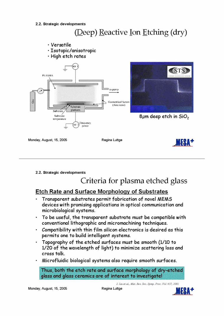
2.2. Strategic developments
(Peep) Reactive Jon Etching (dry)" Versatile" Isotopic/anisotropic" High etch rates
PLASMA
ILL, to PUOIP
Geometrical thctor
I Jr,, Tfl (Area ratio)- 1k' I
Subc:ra /platioMI
Substrite
Immature
jericsRI
Monday, August, 15, 2005 Regina Lutge
_1IESA
2.2. Strategic developments
Criteria for plasma etched glassEtch Rate and Surface MorDholoav of Substrates"
Transparent substrates permit fabrication of novel MEMSdevices with promising applications in optical communication and
microbiological systems." To be useful, the transparent substrate must be compatible with
conventional lithographic and micromachining techniques."
Compatibility with thin film silicon electronics is desired as this
permits one to build intelligent systems." Topography of the etched surfaces must be smooth (1/10 to
1/20 of the wavelength of light) to minimize scattering loss andcross talk.
" Microfluidic biological systems also require smooth surfaces.
Thus, both the etch rate and surface morphology of dry-etchedglass and glass ceramics are of interest to investigate!
J.Lyurta1.,Mat. Rs.2Tc.2mr.Rrrr. 657, 2001
Monday, August, 15, 2005 Regina Luttge
8pm deep etch in 5i02
2.2. Strategic developments
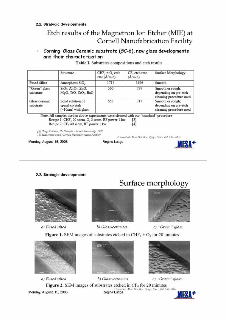
Etch results of the Magnetron Ion Etcher (MIE) atCornell Nanofabrication Facility
"Corning Glass Ceramic substrate (GC-6), new glass developmentsand their characterization
Table I. Substrates compositions and etch results
Structure ClIP3 - 02 etch CF4 etch rate Surface Morphologyrate (Amin) (A!min)
Fused Silica Amorphous SiO, 1714 3676 Smooth
Green" glass Si02. A1203. ZnO. 500 797 Smooth or rough;substrate MgO. TiO. Zr02. BaO depending on pie-etch
cleaning procedure used.Glass-ceramic Solid solution of 553 717 Smooth or rough:substrate spinet crystals depending on pie-etch
(-1 0mm) with glass cleaning procedure used
Note: All samples used m above experiments were cleaned with our --standard procedureRecipe 1: CHF3 20 sccin. 022 sccm. RF power 1 kw [3]Recipe 2: CF- 40 sccm. RF power 1 kw [4]
[3] Greg Wühams, Ph.D thesis, Cornell University, /995
[* 5/Pie .' b o uwrel/I,cooft/n aLonPa 3'5 tol 4Ii 3' ,, 3',, /5'J (If I
Monday, August, 15, 2005 Regina Lutge
2.2. Strategic developments
Surface morphology- w:
.
a
- te a
a a
a) Fused silica hI Glass-ceramics c,) "Green "glass
Figure 1. SEM images of substrates etched iii CT-IF3 + 02 for 20 minutes
-; 'nvPp
40
a) Fused silicab1 Glass-ceramics c) 'Green "glass
Figure 2. SEM images of substrates etched in CF4 for 20 minutes,C Lto it oL,Mat. Fcc :2cc. Swnp. Proc. 14r/.5572U111
Monday, August, 15, 2005 Regina Lutge _JIESA
2.2. Strategic developments
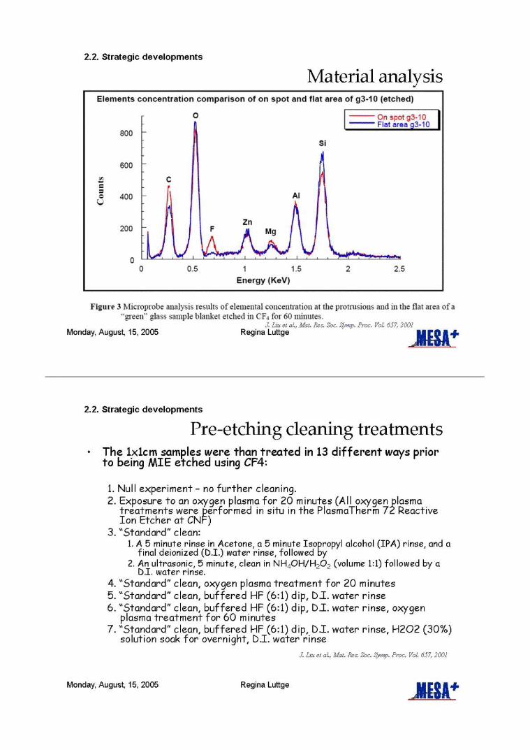
Material analysisElements concentration comparison of on spot and flat area of g3-10 (etched)
0 Onspot g3-10Flat area g3-10
800 -
Si
600 -
C
400-Al
Zn200 - FMg
0"±I!" ,[
0 0.511.522.5
Energy (Key)
Figure 3 Microprobe analysis results of elemental concentration at the protrusions and in the flat area of a"green' glass sample blanket etched in CF4 for 60 minutes.
.C Lo, t A LPrg Soc. Symp. Proc. Vol. 657,2001Monday, August, 15, 2005 Regina Lutge
_1IESA
2.2. Strategic developments
Pre-etching cleaning treatments" The 14cm samples were than treated in 13 different ways prior
to being MIE etched using CF4:
1. Null experiment- no further cleaning.
2. Exposure to on oxygen plasma for 20 minutes (All oxygen plasmatreatments were performed in situ in the PlasmaTherm 72 ReactiveIon Etcher at CNF)
3. Standard" clean:1. A 5 minute rinse in Acetone, a 5 minute Isopropyl alcohol (IPA) rinse, and a
final deionized (DI.) water rinse, followed by2. An ultrasonic, 5 minute, clean in NH4OH/H202 (volume 1:1) followed by a
Di. water rinse.4. "Standard" clean, oxygen plasma treatment for 20 minutes5. "Standard" clean, buffered HF (6:1) dip, D.I. water rinse6. "Standard" clean, buffered HF (6:1) dip, D.I. water rinse, oxygen
plasma treatment for 60 minutes7. "Standard" clean, buffered HF (6:1) dip, Di. water rinse, H202 (30%)
solution soak for overnight, D.I. water rinse
,.Lo,!o1.,1,lLvrSor.Svc'w.P-oc. 14,1. "002
Monday, August, 15, 2005 Regina Lutge J!ESA

2.2. Strategic developments
Treatments (continuous)
8. Buffered HF (6:1) dip, DI. water rinse
9. Buffered HF (6:1) dip, D.I. water rinse, oxygen plasma clean for 20minutes
10. RCA3 cleaning11. RCA cleaning, oxygen plasma treatment for 20 minutes12. RCA cleaning, buffered HF (6:1) dip, D.I. water rinse
13. Treatment 12, oxygen plasma treatment for 20 minutes
I. Lw noL Nor Arc Soc. L)cnp. Proc. Vol. 657, 200]
The RCAclean is commonly set up using series ofbath in which the wafer is immersed. Thefirst bathcontains a mature ofH20/Nff40H/H20, heated to about 7.51C. This solution removes organic residues
from the surface, and also dissolves many metalssuch as Ni, Cd, Zn, Go, Cr, Au andAg [6]
[6] 5 G. Couillard, B C Act, C. Utobach, S M. Blakely, C. B Moore and F P. Fehiner, 7. ojNon-C'rysi. Solids 222 (1997) 429
Monday, August, 15, 2005 Regina Lutge
_1IESA
2.2. Strategic developments
Results of the treatment experiment
After the CF4 etch, only samples cleaned using procedures 5, 6,7, 12, 13 had smooth surfaces. All other samples had a roughsurface and looked opaque (transmission) or milky (reflection).The opaque samples contained a very high density of particles,as shown in Figure 4.
Figure 4. SEM images of etched "green" GC6 glass sample cleaned by procedure #8
S5th ci at, Si5ci. Rca "cc. Syr'cp. Proc. SaL 657, 2001
Monday, August, 15, 2005 Regina Lutge _JESAt
a) SEAL image at x 840 Th SEAL image at x 10900

2.2. Strategic developments
Deep glass etching for feed-through
" Classical MEMS development: spin-off for microfluidic chipfabrication.
"Feed-throughs is one of the key processes in the field ofMEMS.
X U flat. JAIRMO VOL. ii. MO 2002
Monday, August, 15, 2005ReginaLutge _IIESAt
2.2. Strategic developments
a) Preparation of Ni mask for deep RIE
15 am thick Ni mask
Au/Cr seed layerKVI FZZ1 K
Pyrex glass (150/2 m) Ni layer (0.2 11 m)
b) Deep RIE
Ni mask Au/Cr seed layer
IPrex:
Felass
c) Removement of the mask and cleaning
Glass
DRIE for glass
" Sulfur hexafluoride (SF6)plasma.
"Aspect ratios: 5-7 for a hole
pattern and 10 for a trench
pattern.
Through the wafer etching of ahole pattern of 50 mmdiameter was carried out using150mm-thick Pyrex glasswafers.
X Un at.,2MEMO VOL. ii, NO 6, 2002
Monday, August, 15, 2005 Regina Lutge JIESA
2.2. Strategic developments
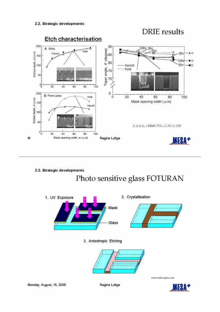
DRIE results
£a
a.0
M
Etch characterisation200 -
A Silica
L:
50.-
40 60 80 100
0
L''JTT
trench
U 20 'i1) 04)
OLiMask opening width. w (urn)
90C)C),85
C)
80
a)o,75CCU
3 70a.CUI-,
OL0
- trench-hole
20 406 doMask opening width (urn)
NLz at al., JMRMS, VOL. II, NO. 6, 2002
00
Regina Lutge
100
a
:00
2.2. Strategic developments
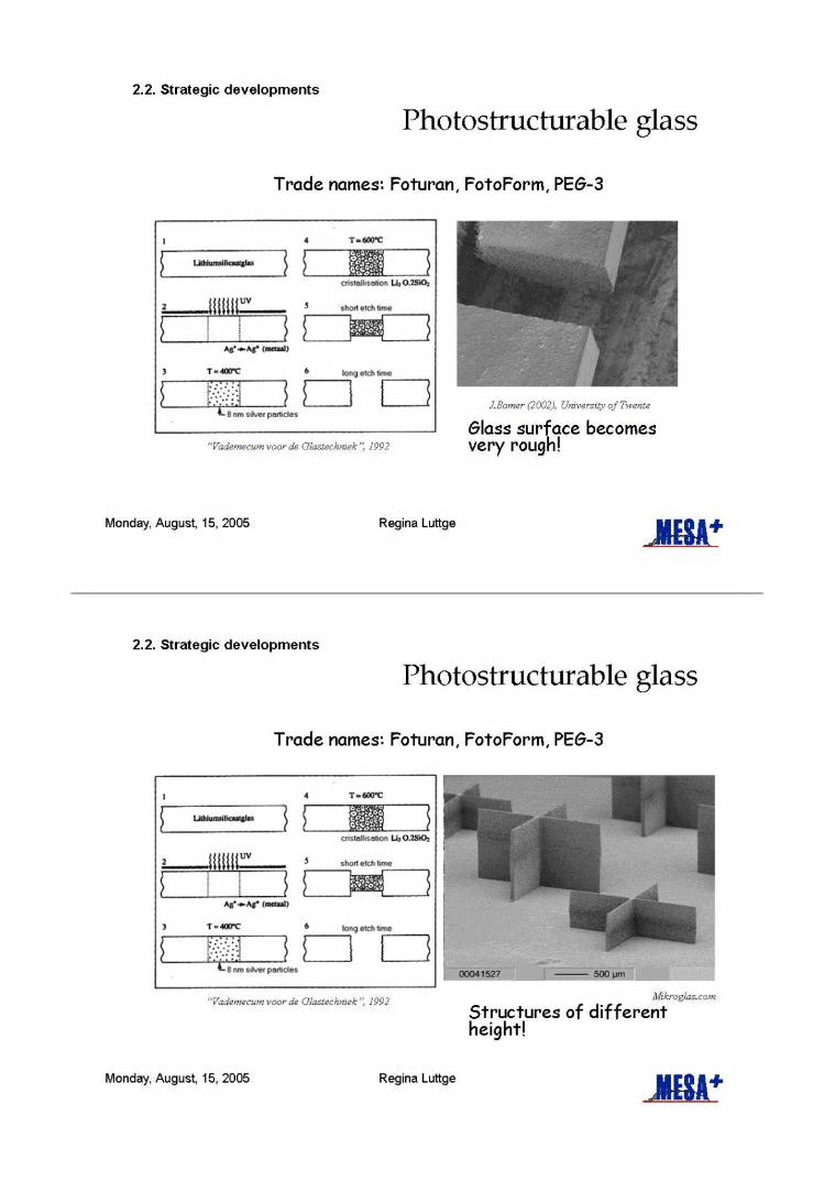
Photo sensitive glass FOTURAN
1. U\ 2. Crystallization
Mask
/....
Glass If'3. Anisotropic Etching
/1www.intkroglas.com
Monday, August, 15, 2005 Regina Lutge
2.2. Strategic developments
Photostructurable glass
Trade names: Foturan, FotoForm, PEG-3
4
tj;InIIisnIiuri Li, 0.2510,
11111 1 UV
U111JUNIM N.2 5 sho,telchhme
AeA( (ml)
S T4OOt6long etch time
nm Over pamcles
"Vademecum voord &'las!rci2n?4c 1992
Monday, August, 15, 2005 Regina Lutge
2.2. Strategic developments
Photostructurable glass
Trade names: Foturan, FotoForm, PEG-3
4 T6®t
rr______H Ii Li,0.2SiO,
2UV
5 shoe etch hme
HS 3PHACA( IrS)
3 T-400'C 6long etch time
no, silver pertcles
"V2dcccur vccrdc OOLlcIcc.9mck 1 1992
2.. k
00041527
5M PM
Aiftroglas.com
Structures of differentheight!
Monday, August, 15, 2005 Regina Lutge J!ESA
,LBcmcr (20012, UnwcrsLycj Twcrdc
Glass surface becomesvery rough!
2.2. Strategic developments
Powder blasting" Unconventional technique (not allowed in cleanroom)
f Pressurized air mixture1-5 Bar
Average particle size:3-3Omicron
(V
= 80-290 rn/s
____Mask
Roughness0.2-2.5 micron Target
21., Jnn'0rVy of' eite
Monday, August, 15, 2005ReginaLuttge
2.2. Strategic developments
Powder blasting properties
" Etch rate is about 20 gm/min, minimum feature size isabout 30 gm.
" Suitable for any brittle material (silicon, glass, ceramics)" Mask material is rubber foil or a thick metal layer.
deeper compared tosmaller channels.r!!,'711
Blast lag a widerchannel became Very suitable to
make throughholes
i-OkV
H Woosmx,FhL Thoss. U2n'onoyf ilt'o.'!to,2002
Monday, August, 15, 2005 Regina Luttge
Single particle impact
Maximum depthto width ratio is
2.2. Strategic developments
Critical Dimensions in powder blasting
S.!VV O.
_ S SS
-
ma-
a IIH. K'r?mTrA., PhD
Monday, August, 15, 2005 Regina LuttTh'ss. Unw'rs?!)oJ TwQ.'!t', 2002
ge JIESAt
2.2. Strategic developments
Monday, August, 15, 2005 Regina Luttge
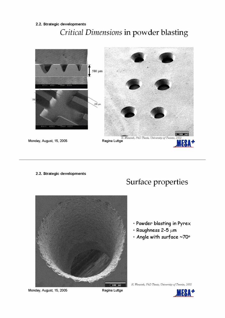
Surface properties
" Powder blasting in Pyrex" Roughness 2-5 jim"Angle with surface t7O0
H. WensnA; PhD Thn4 U?0vQrs4y ofTwete, 2002
Topics in this section
Glass devices
Thin-film processing versushulk...no simple answers!
Monday, August, 15, 2005
- Integrated Circuit (IC) processingphilosophy,
- Combined techniques.
Regina Luttge
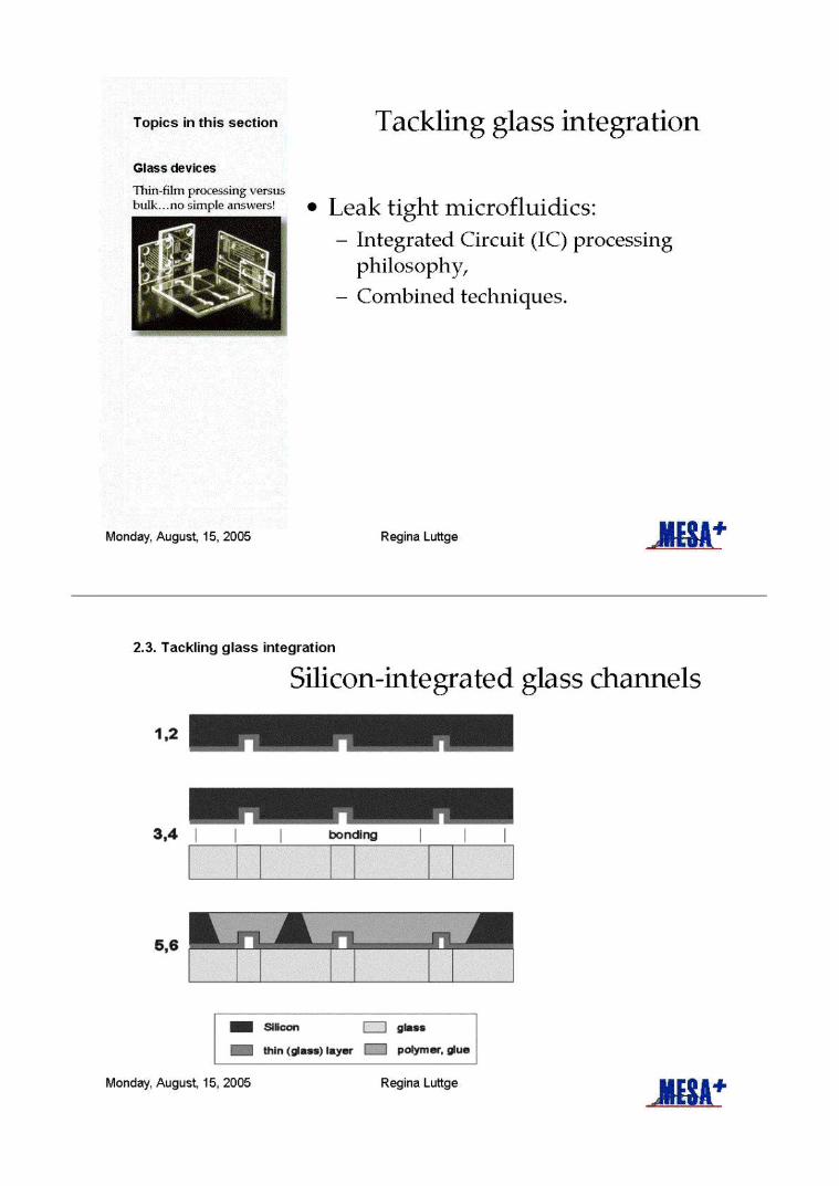
2.3. Tackling glass integration
Tackling glass integration
" Leak tight microfluidics:
Silicon-integrated glass channels
1,2
3,4 bonding
tI.tpn5,6
- Slicon
glass
thin (glass) layer El polymer, glue
Monday, August, 15, 2005 Regina Lutge JIESA
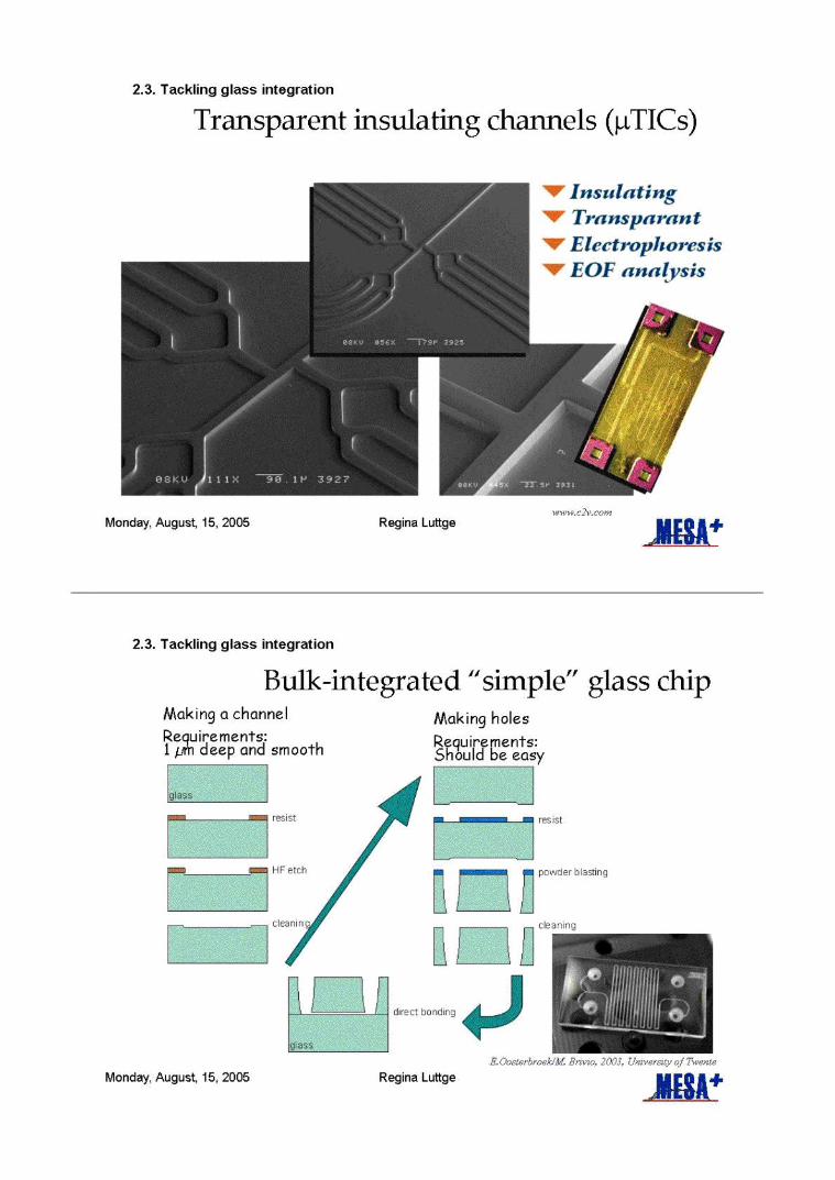
2.3. Tackling glass integration
Transparent insulating channels QiTICs)
sulating'ansparan tectropisoresis)F analysis
/
Monday, August, 15, 2005 Regina Lutgerttrr. ir'.
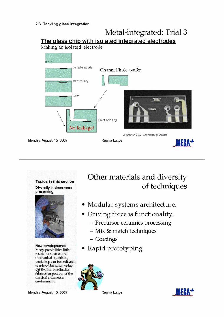
2.3. Tackling glass integration
Bulk-integrated "simple" glass chipMaking a channel
Requirements:1 pm deep and smooth
glass
r resist
p
p
HF etch
F_I
Monday, August, 15, 2005
Making holes
Requirements:Should be easy
resist
powder blastirip
mm ctssninq
k direct bonding a -glass S 'a
E.000wrbr05 r --
Regina Lutge MESAt

2.3. Tackling glass integration
Metal-integrated: Trial 1The glass chip with integrated electrodes
Making an electrode
Requirements: metal
glassChannel/hole wafer
Tmetal spu ttsri ri'-
- 'llsarirnq
Monday, August, 15, 2005 Regina Lutge
akage
ding
2.3. Tackling glass integration
Metal-integrated: Trial 2The glass chip with integrated electrodes
Making a buried electrode
glassH F etch
metal sputtering
Channel/hole wafer
~ E~
Stillleakageling
Monday, August, 15, 2005 Regina Lutge JIESA
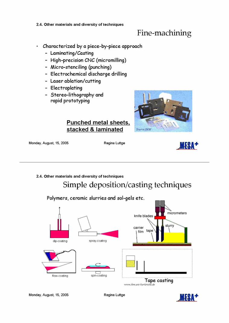
2.3. Tackling glass integration
Metal-integrated: Trial 3The glass chip with isolated integrated electrodesMaking an isolated electrode
glass
Lu
PE(--,,'El SiO
Channel/hole wafer
~ E71
\\\ r m,_,,,,,
11.4 P
direct bonding
No leakage!
Monday, August, 15, 2005 Regina Lutge
B. (roune, 2003, 1'003' 03' 33V0nEC
Topics in this section
Diversity in clean roomprocessing
'V~iNew developmentsMany possibilities littlerestrictions- an entiremechanical machiningworkshop canbe dedicatedto microfabri cation today.Off-limits: microfluidicsfabrication gets out of theclassical cleanroomenvironment,
Monday, August, 15, 2005
Other materials and diversityof techniques
" Modular systems architecture." Driving force is functionality.
- Precursor ceramics processing- Mix & match techniques- Coatings
" Rapid prototyping
Regina Luttge
2.4. Other materials and diversity of techniques
Fine-machiningCharacterized by a piece-by-piece approach-
Laminating/Casting-
High-precision CNC (micromilling)-
Micro-stenciling (punching)- Electrochemical discharge drilling- Laser ablation/cutting-
Electroplating- Stereo-lithography and
rapid prototyping
Punched metal sheetsstacked & laminated
Monday, August, 15, 2005
Source:ZMM
Regina Luttge
2.4. Other materials and diversity of techniques
Simple deposition/casting techniquesPolymers, ceramic slurries and sol-gels etc.
micrometersknife blades
slurrycarrier\film tape,
dip-coating spray-coating
flow-coating spin-coating
Tape casting
Monday, August, 15, 2005 Regina Lutge JIESA

2.4. Other materials and diversity of techniques
Laminating
"Laminating is a process for bonding sheets of materials
together to produce large multi-layer panels." Adhesive is usually applied to the bonding surfaces and the
sheets are stacked in some kind of press which compressesthe panel while the adhesive cures.
" The sheets can also be bonded by other means, e.g. thermo-
compression bonding of stainless steel.
C
Monday, August, 15, 2005 Regina Lutge
2.4. Other materials and diversity of techniques
Laminating
" Laminatii
together" Adhesivc
sheets athe pane
" The shed
compres
Monday, August, 15, 2005
Develops mutt-channelreactors fee tent-ye-relatedapplications includes ccreformers, hydrogen -p-1,-and heat e charge
Severe i E2 (hi kii ii -d oil L ortainu ton I nchroloqyContact David Airssan
The ultimate goal of this research is to produce a prototype micro-reactor reformerand a hydrogen filter for fuel cell applications for testing.
ARC micro-reactors are fabricated via a process called micro-lamination, the bondingof sequentially layered, precision-machined foils or sheets. Micro-laminationconsists of 3 processing steps:
Precision machining of metallic shoots to contain the complex internal
features of the device,
" Registration or staclatg each machined laminate in the appropriate
sequence to produce the device math the desired architecture, and
Bonding the stacked foils to produce a solid component consisting of
complex internal features
http://www. alrc.doe. gov/
Regina Lutge J!ESAt
Albany Research Center
2.4. Other materials and diversity of techniques
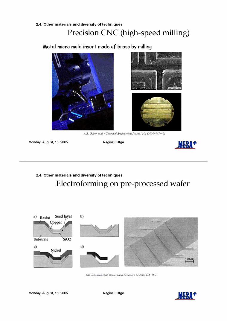
Precision CNC (high-speed milling)Metal micro mold insert made of brass by milling
I
AR. C0tb' ¬r al. / ;alR rmy Jozr'2j LJ1
Monday, August, 15, 2005
Regina Lutge
2.4. Other materials and diversity of techniques
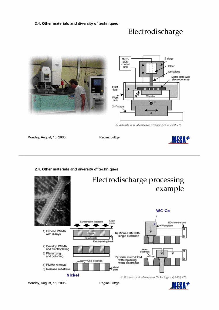
Electroforming on pre-processed wafer
a) Rcsist Seed layer
CopN
Substrate Si02
Nickel
h)
d)
"q%~=-/I
L.R. .lohanscn et aL Sensors andActuators 832000 156-160
Monday, August, 15, 2005 Regina Lutge JIESA
2.4. Other materials and diversity of techniques
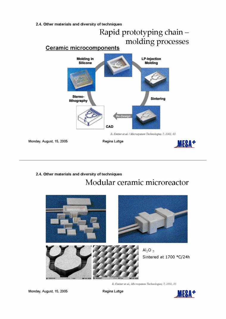
Worktank
X-Y stage
MS
EDMfluid
Electrodischarge
Micro- I-1------i 1stageEDM Icontrol
unit Holder
Workp
Metal plate withelectrode array
4)x
Monday, August, 15, 2005 Regina Lutge
K. Talcahala at al. A&rovstem Tacknolagi&s, o 2000, 175
2.4. Other materials and diversity of techniques
' Electrodischarge processingr example
p- I EDMnttolunit
wokoooe
l)Expose PMMA
X-rays L s:Ee1k 6) Micro-EDM withsingle electrode
2) Develop PMMAand electroplating Worn
3) Planartztn9
- electrodeN
and polishing 7) Serial micro-EDM9
with rerad
4) PMMA removal
5) Release substrateMenu
__n131e
Nic el K Thkalnala at al. Mcra'alern TechecIoges, 6,2000,2000,175
Monday, August, 15, 2005 Regina Lutge jE$A!.
2.4. Other materials and diversity of techniques
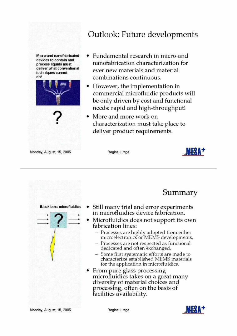
Rapid prototyping chain -
molding processesCeramic microcomnonents
Molding inSilicone
Stereo-
lithography
aMonday, August, 15, 2005
ra LIP-InjectionMolding
'no
CAD
FL Knitter t at)EFcroysn Thciioog's,7. 2001, 55
Regina Lutge JIESAt
2.4. Other materials and diversity of techniques
Modular ceramic microreactor
A120
Sintered at 1700 °C/24h
DQOS1M
IMFmkER
F,. Km-'ere, at, 51kmystE'ia Technol2ges, 7, 2001, 55
Monday, August, 15, 2005 Regina Lutge JIESA
Elf"
Outlook: Future developments
Micro-and nanofabricateddevices to containandprocess liquids mustdeliver what conventional
techniques cannotdo!
?
Monday, August, 15, 2005
" Fundamental research in micro-andnanofabrication characterization forever new materials and materialcombinations continuous.
" However, the implementation incommercial microfluidic products willbe only driven by cost and functionalneeds: rapid and high-throughput!
" More and more work oncharacterization must take place todeliver product requirements.
Regina Luttge
SummaryBlack box: microlluidics " Still many trial and error experiments
in microfluidics device fabrication." Microfluidics does not support its own
"fabrication lines:/1 - Processes are highly adopted from either
microelectronics or MEMS developments,- Processes are not respected as functional
dedicated and often exchanged,\
' - Some first systematic efforts are made tocharacterize established MEMS materialsfor the application in microfluidics,
" From pure glass processingmicrofluidics takes on a great manydiversity of material choices and
Frocessing, often on the basis ofacilities availability.
Monday, August, 15, 2005 Regina Luttge JIESA