introduction to electronic design automation testing
TRANSCRIPT
1
Introduction to Electronic Design Automation
Jie-Hong Roland Jiang江介宏
Department of Electrical EngineeringNational Taiwan University
Spring 2013
2
Testing
Slides are by Courtesy of Prof. S.-Y. Huang and C.-M. Li
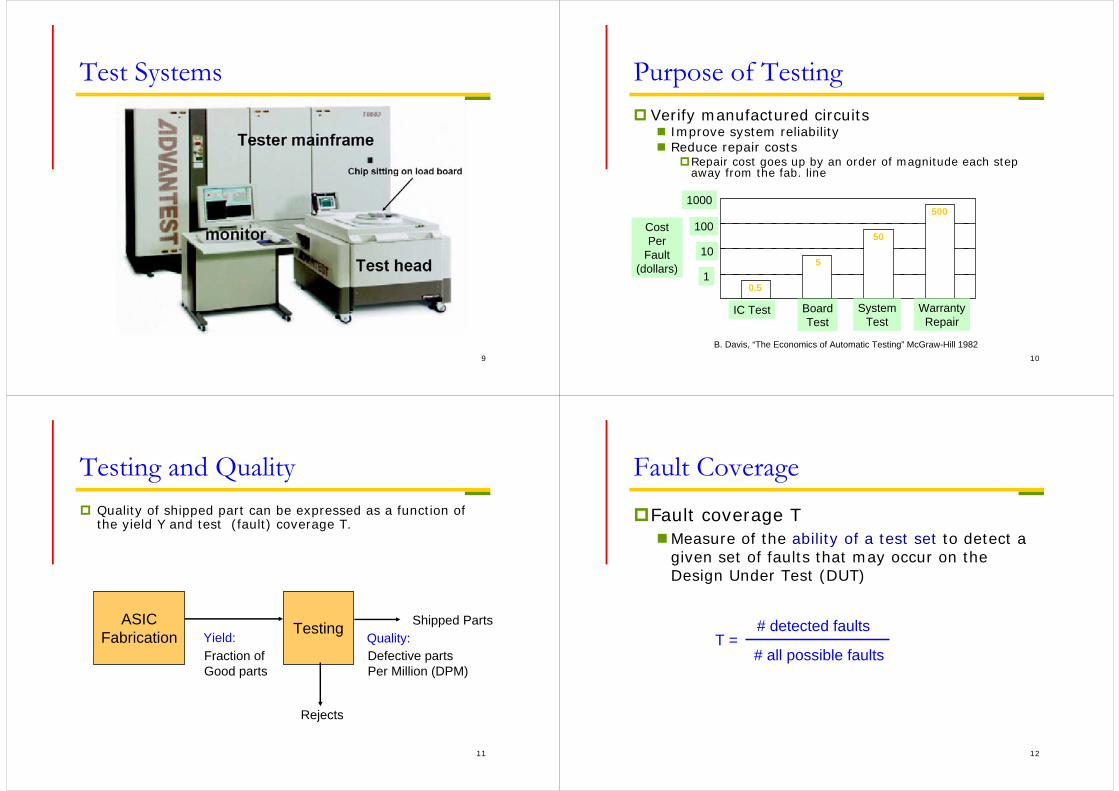
3
Testing Recap
Design verificationIs what I specified really what I wanted?
Property checking
Implementation verificationIs what I implemented really what I specified?
Equivalence checking
Manufacture verificationIs what I manufactured really what I implemented?
Testing; post manufacture verification Quality control
Distinguish between good and bad chips
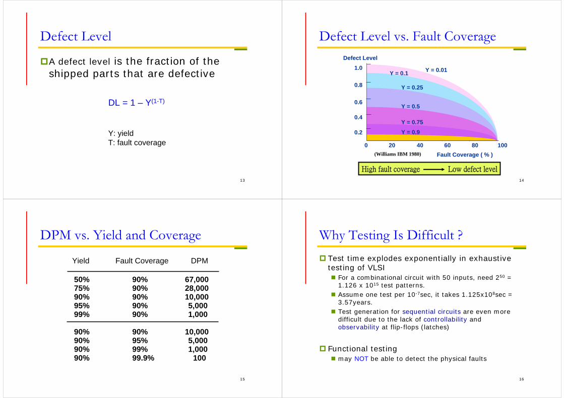
4
Design Flow
Idea
Architecture Design
Circuit & Layout Design
Blockdiagram
Layout
IC Fabrication
Wafer(hundreds of dies)
Sawing & Packaging
Final chips
Final Testing
Bad chips Good chipscustomers
5
Manufacturing Defects Processing faults
missing contact windows parasitic transistors oxide breakdown
Material defects bulk defects (cracks, crystal imperfections) surface impurities
Time-dependent failures dielectric breakdown electro-migration
Packaging failures contact degradation seal leaks
6
Faults, Errors and Failures Faults
A physical defect within a circuit or a system May or may not cause a system failure
Errors Manifestation of a fault that results in incorrect circuit (system)
outputs or states Caused by faults
Failures Deviation of a circuit or system from its specified behavior Fail to do what is supposed to do Caused by errors
Faults cause errors; errors cause failures
7
Testing and Diagnosis
Testing Exercise a system and analyze the response to
ensure whether it behaves correctly after manufacturing
Diagnosis Locate the causes of misbehavior after the
incorrectness is detected
8
Scenario of Manufacturing TestTEST VECTORS
ManufacturedCircuits
Comparator
CIRCUIT RESPONSE
PASS/FAILCORRECTRESPONSES
9
Test Systems
10
Purpose of Testing Verify manufactured circuits
Improve system reliability Reduce repair costs
Repair cost goes up by an order of magnitude each step away from the fab. line
0.5
5
50
500
ICTest
BoardTest
SystemTest
WarrantyRepair
10
1
100
1000
Costper
fault(Dollars)
B. Davis, “The Economics of Automatic Testing” McGraw-Hill 1982
IC Test BoardTest
SystemTest
WarrantyRepair
CostPer
Fault(dollars)
1
10
1000
100
11
Testing and Quality Quality of shipped part can be expressed as a function of
the yield Y and test (fault) coverage T.
ASICFabrication Testing
Yield:Fraction ofGood parts
Rejects
Shipped PartsQuality:Defective partsPer Million (DPM)
12
Fault Coverage
Fault coverage TMeasure of the ability of a test set to detect a
given set of faults that may occur on the Design Under Test (DUT)
T = # detected faults
# all possible faults
13
Defect Level
A defect level is the fraction of the shipped parts that are defective
DL = 1 – Y(1-T)
Y: yieldT: fault coverage
14
Defect Level vs. Fault CoverageDefect Level
Fault Coverage ( % )0 20 40 60 80 100
0.2
0.4
0.6
0.8
1.0 Y = 0.01Y = 0.1
Y = 0.25
Y = 0.5
Y = 0.75Y = 0.9
(Williams IBM 1980)
High fault coverage Low defect level
15
DPM vs. Yield and Coverage
50% 90% 67,00075% 90% 28,00090% 90% 10,00095% 90% 5,00099% 90% 1,000
90% 90% 10,00090% 95% 5,00090% 99% 1,00090% 99.9% 100
Fault CoverageYield DPM
16
Why Testing Is Difficult ? Test time explodes exponentially in exhaustive
testing of VLSI For a combinational circuit with 50 inputs, need 250 =
1.126 x 10¹⁵ test patterns. Assume one test per 10-7sec, it takes 1.125x10⁸sec =
3.57years. Test generation for sequential circuits are even more
difficult due to the lack of controllability and observability at flip-flops (latches)
Functional testing may NOT be able to detect the physical faults
17
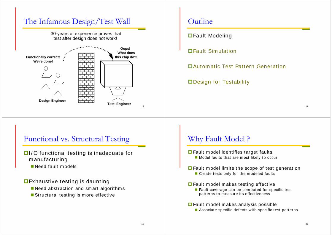
The Infamous Design/Test Wall30-years of experience proves that
test after design does not work!
Functionally correct!We're done!
Oops!What does
this chip do?!
Design EngineerTest Engineer
18
Outline
Fault Modeling
Fault Simulation
Automatic Test Pattern Generation
Design for Testability
19
Functional vs. Structural Testing
I/O functional testing is inadequate for manufacturingNeed fault models
Exhaustive testing is dauntingNeed abstraction and smart algorithms Structural testing is more effective
20
Why Fault Model ? Fault model identifies target faults
Model faults that are most likely to occur
Fault model limits the scope of test generation Create tests only for the modeled faults
Fault model makes testing effective Fault coverage can be computed for specific test
patterns to measure its effectiveness
Fault model makes analysis possible Associate specific defects with specific test patterns
21
Fault Modeling vs. Physical Defects
Fault modelingModel the effects of physical defects on the
logic function and timing
Physical defectsSilicon defects Photolithographic defectsMask contamination Process variationDefective oxides
22
Fault Modeling vs. Physical Defects (cont’d)
Electrical effects Shorts (bridging faults) Opens Transistor stuck-on/open Resistive shorts/opens Change in threshold voltages
Logical effects Logical stuck-at-0/1 Slower transition (delay faults) AND-bridging, OR-bridging
23
Typical Fault Types
Stuck-at faultsBridging faultsTransistor stuck-on/open faultsDelay faultsIDDQ faultsState transition faults (for FSM)Memory faultsPLA faults
24
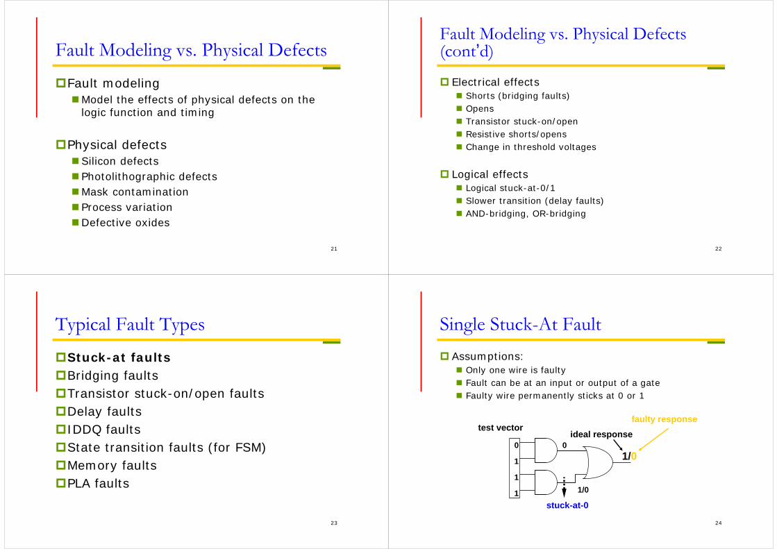
Single Stuck-At Fault Assumptions:
Only one wire is faulty Fault can be at an input or output of a gate Faulty wire permanently sticks at 0 or 1
0
1
1
1
0
1/0
1/0
stuck-at-0
ideal responsetest vector
faulty response
25
Multiple Stuck-At Faults
Several stuck-at faults occur at the same time Common in high density circuits
For a circuit with k lines There are 2k single stuck-at faults There are 3k-1 multiple stuck-at faults
A line could be stuck-at-0, stuck-at-1, or fault-freeOne out of 3k resulting circuits is fault-free
26
Why Single Stuck-At Fault Model ? Complexity is greatly reduced
Many different physical defects may be modeled by the same logical single stuck-at fault
Stuck-at fault is technology independent Can be applied to TTL, ECL, CMOS, BiCMOS etc.
Design style independent Gate array, standard cell, custom design
Detection capability of un-modeled defects Empirically, many un-modeled defects can also be
detected accidentally under the single stuck-at fault model
Cover a large percentage of multiple stuck-at faults
27
Why Logical Fault Modeling ? Fault analysis on logic rather than physical problem
Complexity is reduced
Technology independent Same fault model is applicable to many technologies Testing and diagnosis methods remain valid despite changes in
technology
Wide applications The derived tests may be used for physical faults whose effect
on circuit behavior is not completely understood or too complex to be analyzed
Popularity Stuck-at fault is the most popular logical fault model
28
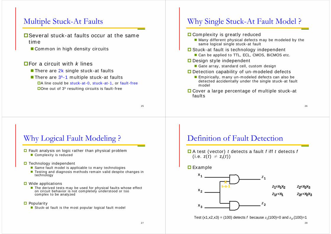
Definition of Fault Detection A test (vector) t detects a fault f iff t detects f
(i.e. z(t) ≠ zf(t))
Example
xX1
X2
X3
Z1
Z2
s-a-1 Z1=X1X2 Z2=X2X3
Z1f =X1 Z2f =X2X3
Test (x1,x2,x3) = (100) detects f because z1(100)=0 and z1f (100)=1
29
Fault Detection Requirement A test t that detects a fault f
activates f (or generate a fault effect) by creating different v and vf values at the site of the fault
propagates the error to a primary output z by making all the wires along at least one path between the fault site and z have different v and vf values
Sensitized wire A wire whose value in response to the test changes in
the presence of the fault f is said to be sensitized by the test in the faulty circuit
Sensitized path A path composed of sensitized wires is called a
sensitized path
30
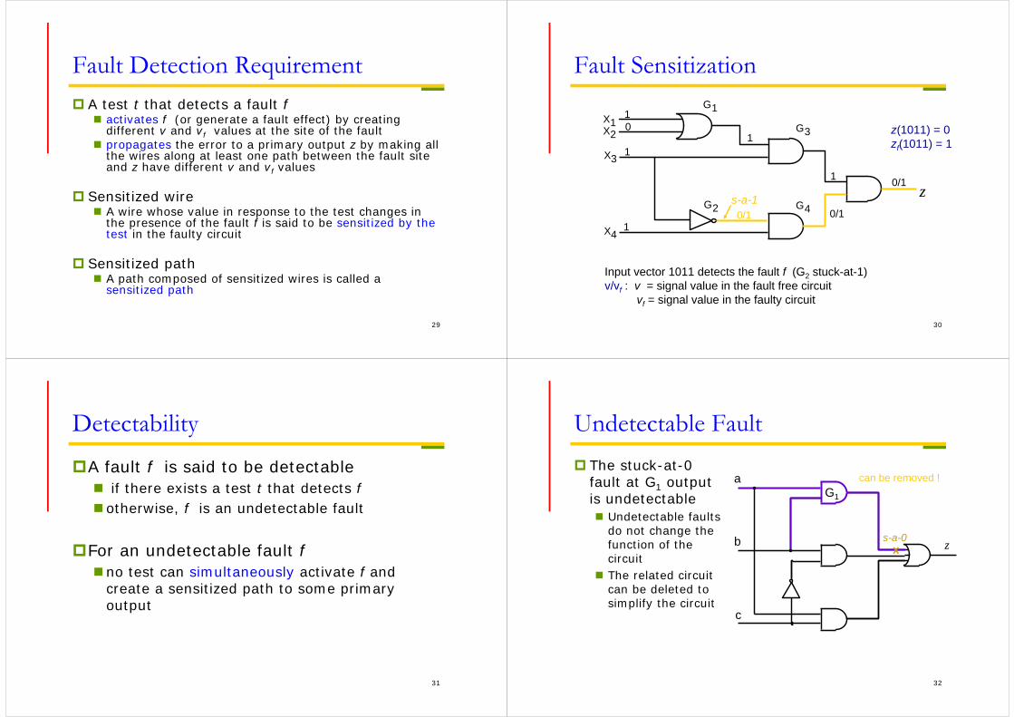
Fault Sensitization
Input vector 1011 detects the fault f (G2 stuck-at-1)v/vf : v = signal value in the fault free circuit
vf = signal value in the faulty circuit
X1X2
X3
X4
G1
G2
G3
G4
10
1
1
1
s-a-10/1
1
0/1
0/1 z
z(1011) = 0zf(1011) = 1
31
Detectability
A fault f is said to be detectable if there exists a test t that detects f otherwise, f is an undetectable fault
For an undetectable fault f no test can simultaneously activate f and
create a sensitized path to some primary output
32
Undetectable Fault The stuck-at-0
fault at G1 output is undetectable Undetectable faults
do not change the function of the circuit
The related circuit can be deleted to simplify the circuit
s-a-0
a
b
c
z
can be removed !
x
G1
33
Test Set Complete detection test set
A set of tests that detects any detectable fault in a designated set of faults
Quality of a test set is measured by fault coverage
Fault coverage Fraction of the faults detected by a test set can be determined by fault simulation >95% is typically required under the single stuck-at
fault model >99.9% required in the ICs manufactured by IBM
34
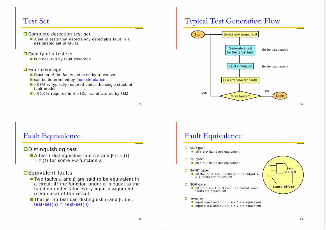
Typical Test Generation FlowSelect next target fault
Generate a testfor the target fault
Discard detected faults
More faults ? Done
Fault simulation
Start
yes no
(to be discussed)
(to be discussed)
35
Fault EquivalenceDistinguishing testA test t distinguishes faults and if z(t)
≠z(t) for some PO function z
Equivalent faults Two faults and are said to be equivalent in
a circuit iff the function under is equal to the function under for every input assignment (sequence) of the circuit.
That is, no test can distinguish and , i.e., test-set() = test-set()
36
Fault Equivalence AND gate:
all s-a-0 faults are equivalent
OR gate: all s-a-1 faults are equivalent
NAND gate: all the input s-a-0 faults and the output s-
a-1 faults are equivalent
NOR gate: all input s-a-1 faults and the output s-a-0
faults are equivalent
Inverter: input s-a-1 and output s-a-0 are equivalent input s-a-0 and output s-a-1 are equivalent
xx
s-a-0s-a-0
same effect

37
Equivalence Fault Collapsing
n+2, instead of 2(n+1), single stuck-at faults need to be considered for n-input AND (or OR) gates
s-a-1
s-a-1
s-a-1
s-a-1
s-a-1
s-a-1
s-a-1
s-a-1
s-a-0
s-a-0
s-a-0
s-a-0
s-a-0
s-a-0
s-a-0
s-a-0
38
Equivalent Fault Group In a combinational circuit
Many faults may form an equivalence group These equivalent faults can be found in a reversed
topological order from POs to PIs
s-a-1
s-a-0 s-a-1
x
x x
Three faults shown are equivalent !
39
Fault Dominance Dominance relation
A fault is said to dominate another fault in an irredundant circuit iff every test (sequence) for is also a test (sequence) for i.e., test-set() test-set()
No need to consider fault for fault detection
Test() Test() is dominated by
40
Fault Dominance AND gate
Output s-a-1 dominates any input s-a-1
NAND gate Output s-a-0 dominates any input s-a-1
OR gate Output s-a-0 dominates any input s-a-0
NOR gate Output s-a-1 dominates any input s-a-0
Dominance fault collapsing Reducing the set of faults to be analyzed based on the
dominance relation
xx
s-a-1s-a-1
easier to test
harder to test
41
Stem vs. Branch Faults Detect A s-a-1:
z(t)zf(t) = (CDCE)(DCE) = DCD (C=0,D=1)
Detect C s-a-1:z(t)zf(t) = (CDCE)(DE) (C=0,D=1,E=0) or (C=0,D=0,E=1)
Hence, C s-a-1 does not dominate A s-a-1
In general, there might be no equivalence or dominance relations between stem and branch faults
A
B
C
D
Ex
x
x
C: stem of a multiple fanoutA, B: branches
42
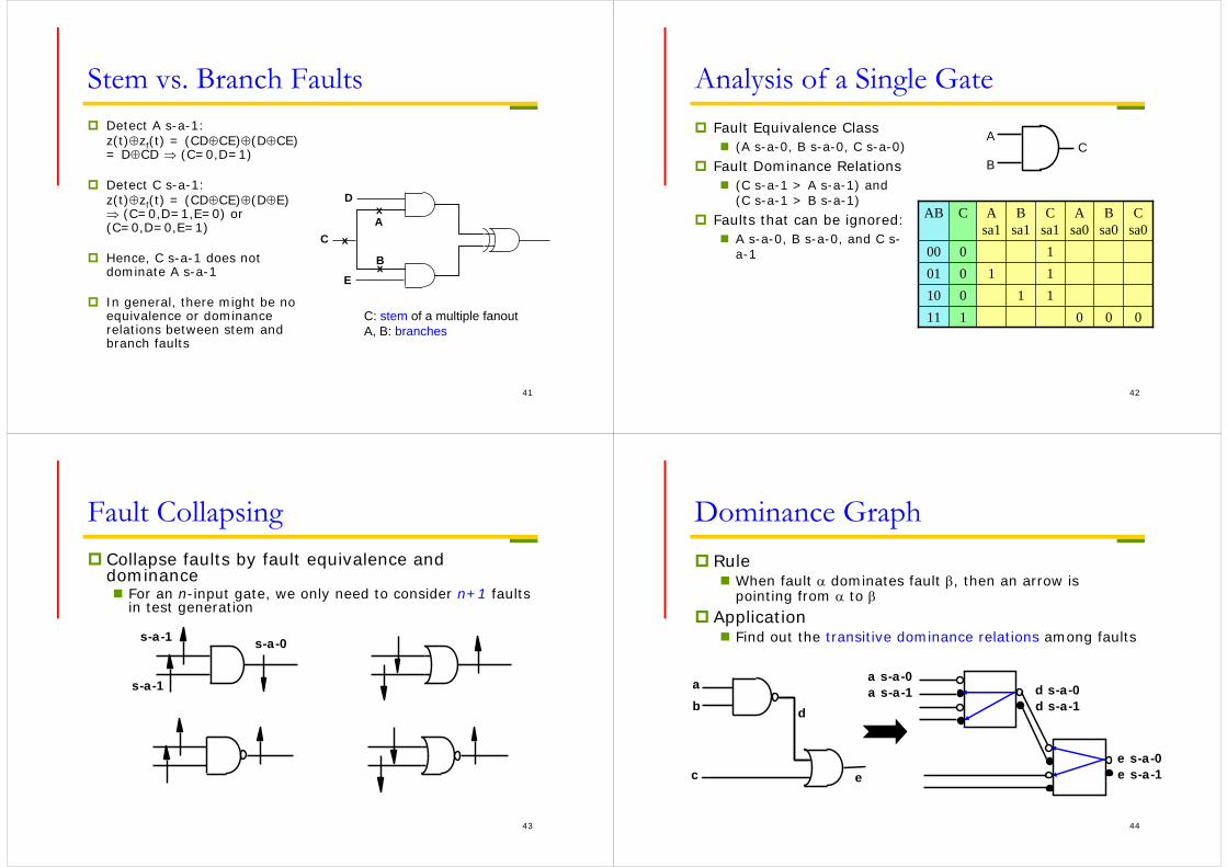
Analysis of a Single Gate Fault Equivalence Class
(A s-a-0, B s-a-0, C s-a-0) Fault Dominance Relations
(C s-a-1 > A s-a-1) and (C s-a-1 > B s-a-1)
Faults that can be ignored: A s-a-0, B s-a-0, and C s-
a-1
A
BC
11100100
AB
0
A sa0
0
B sa0
11001
11010
C sa0
C sa1
B sa1
A sa1
C
43
Fault Collapsing Collapse faults by fault equivalence and
dominance For an n-input gate, we only need to consider n+1 faults
in test generation
s-a-0s-a-1
s-a-1
44
Dominance Graph Rule
When fault dominates fault , then an arrow is pointing from to
Application Find out the transitive dominance relations among faults
d s-a-0d s-a-1
e s-a-0e s-a-1
ab d
c e
a s-a-0a s-a-1
45
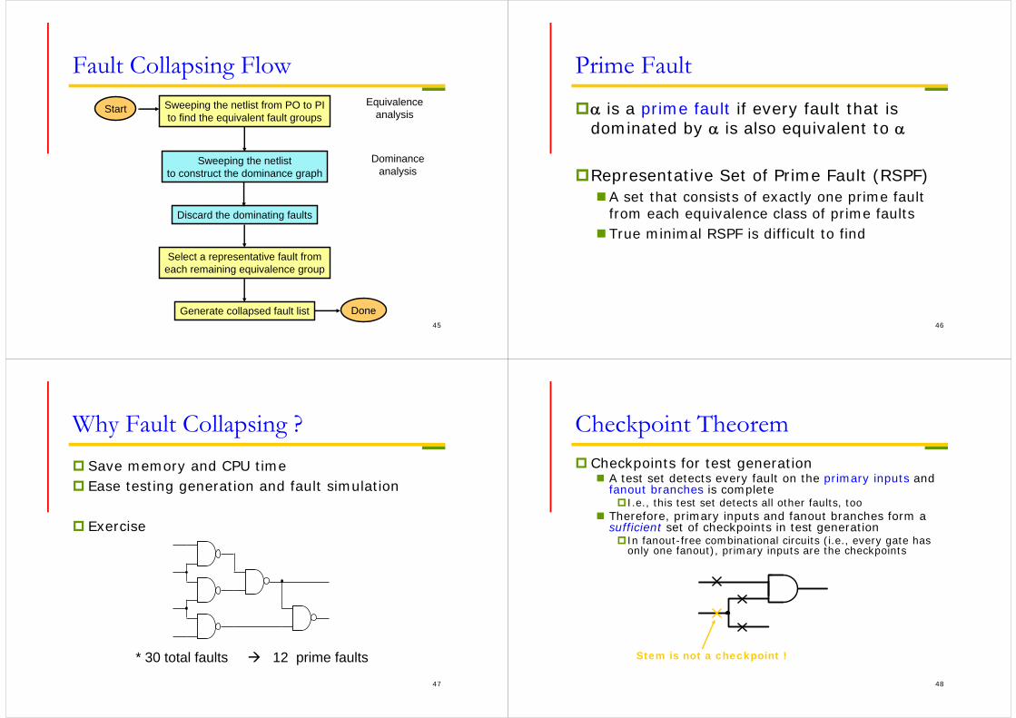
Fault Collapsing Flow
Select a representative fault fromeach remaining equivalence group
Done
Discard the dominating faults
Start Sweeping the netlist from PO to PIto find the equivalent fault groups
Equivalenceanalysis
Sweeping the netlistto construct the dominance graph
Dominanceanalysis
Generate collapsed fault list46
Prime Fault is a prime fault if every fault that is
dominated by is also equivalent to
Representative Set of Prime Fault (RSPF)A set that consists of exactly one prime fault
from each equivalence class of prime faults True minimal RSPF is difficult to find
47
Why Fault Collapsing ? Save memory and CPU time Ease testing generation and fault simulation
Exercise
* 30 total faults 12 prime faults
48
Checkpoint Theorem Checkpoints for test generation
A test set detects every fault on the primary inputs and fanout branches is completeI.e., this test set detects all other faults, too
Therefore, primary inputs and fanout branches form a sufficient set of checkpoints in test generationIn fanout-free combinational circuits (i.e., every gate has
only one fanout), primary inputs are the checkpoints
Stem is not a checkpoint !

49
Why Inputs + Branches Are Enough ? Example
Checkpoints are marked in blue Sweeping the circuit from PI to PO to examine every
gate, e.g., based on an order of (A->B->C->D->E) For each gate, output faults are detected if every input
fault is detected
A
B
C
D
E
a
50
Fault Collapsing + Checkpoint Example:
10 checkpoint faults a s-a-0 <=> d s-a-0 , c s-a-0 <=> e s-a-0
b s-a-0 > d s-a-0 , b s-a-1 > d s-a-1 6 faults are enough
a
b
c
d
e
f
g
h
51
Outline
Fault Modeling
Fault Simulation
Automatic Test Pattern Generation
Design for Testability
52
Why Fault Simulation ?To evaluate the quality of a test set I.e., to compute its fault coverage
Part of an ATPG programA vector usually detects multiple faults Fault simulation is used to compute the faults
that are accidentally detected by a particular vector
To construct fault-dictionary For post-testing diagnosis
53
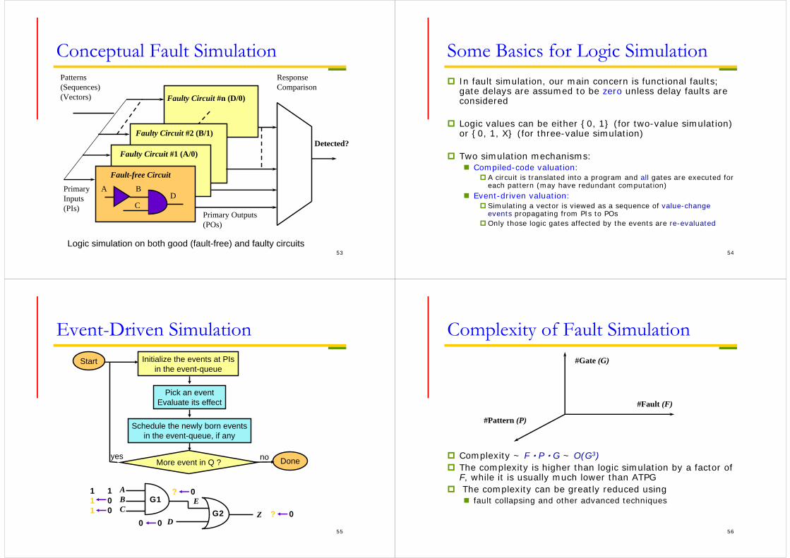
Conceptual Fault Simulation
Fault-free Circuit
Faulty Circuit #1 (A/0)
Faulty Circuit #2 (B/1)
Faulty Circuit #n (D/0)
PrimaryInputs(PIs)
Primary Outputs(POs)
Patterns(Sequences)(Vectors)
Response Comparison
Detected?
A B
CD
Logic simulation on both good (fault-free) and faulty circuits54
Some Basics for Logic Simulation In fault simulation, our main concern is functional faults;
gate delays are assumed to be zero unless delay faults are considered
Logic values can be either {0, 1} (for two-value simulation) or {0, 1, X} (for three-value simulation)
Two simulation mechanisms: Compiled-code valuation:
A circuit is translated into a program and all gates are executed for each pattern (may have redundant computation)
Event-driven valuation: Simulating a vector is viewed as a sequence of value-change
events propagating from PIs to POsOnly those logic gates affected by the events are re-evaluated
55
Event-Driven SimulationInitialize the events at PIs
in the event-queue
Pick an eventEvaluate its effect
More event in Q ? Done
Schedule the newly born eventsin the event-queue, if any
Start
yes no
ABC
EZ
D
100
111
0 0
? 0
? 0
G1G2
56
Complexity of Fault Simulation
Complexity ~ F‧P‧G ~ O(G3) The complexity is higher than logic simulation by a factor of
F, while it is usually much lower than ATPG The complexity can be greatly reduced using
fault collapsing and other advanced techniques
#Gate (G)
#Pattern (P)
#Fault (F)
57
Characteristics of Fault Simulation Fault activity with respect to fault-free circuit
is often sparse both in time and space. For example
F1 is not activated by the given pattern, while F2 affects only the lower part of this circuit.
0
1
1
F1(s-a-0)
F2(s-a-0)×
×
58
Fault Simulation Techniques
Parallel Fault SimulationDeductive Fault Simulation
59
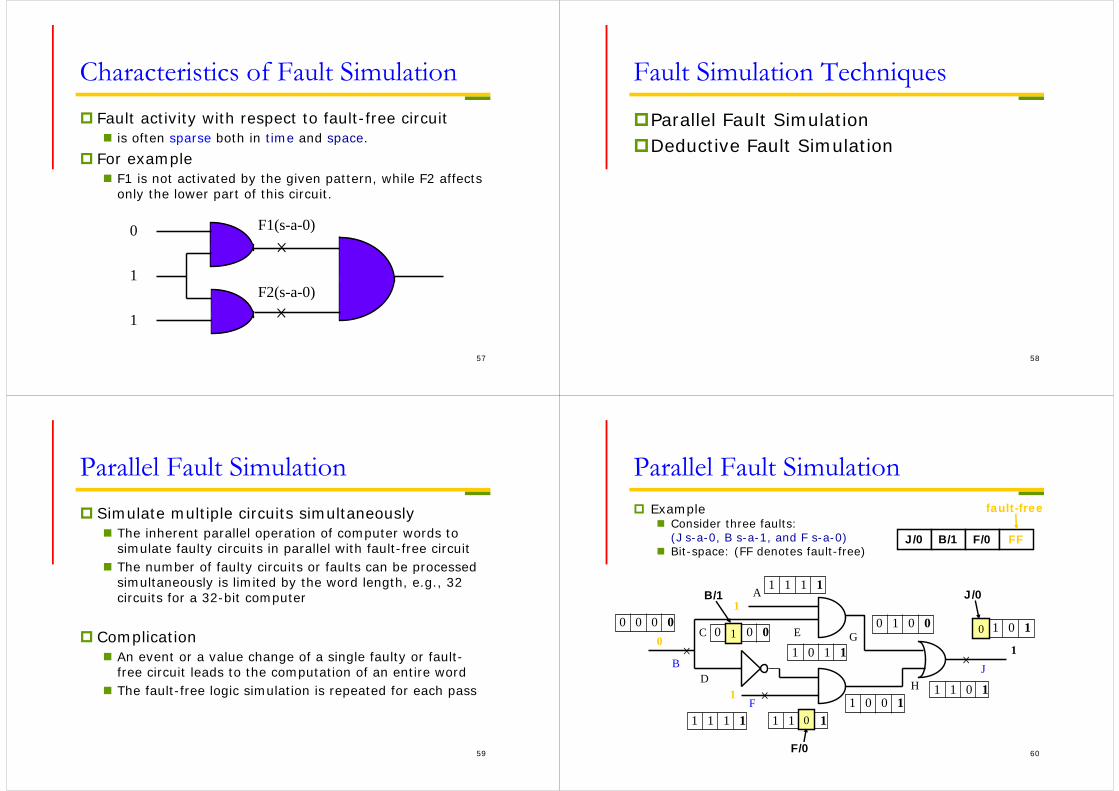
Parallel Fault Simulation Simulate multiple circuits simultaneously
The inherent parallel operation of computer words to simulate faulty circuits in parallel with fault-free circuit
The number of faulty circuits or faults can be processed simultaneously is limited by the word length, e.g., 32 circuits for a 32-bit computer
Complication An event or a value change of a single faulty or fault-
free circuit leads to the computation of an entire word The fault-free logic simulation is repeated for each pass
60
Parallel Fault Simulation Example
Consider three faults: (J s-a-0, B s-a-1, and F s-a-0)
Bit-space: (FF denotes fault-free)
A
B
C
D
E
F
G
HJ
1
0
1
1
0 0 0 00 1 0 0
1 1 1 1
1 0 0 1
0 1 0 0 0 1 0 1
1 1 0 11 1 1 1
1 1 0 1
1 0 1 1
J/0 B/1 F/0 FF
F/0
J/0B/1
fault-free
×
××
1
0
0
61
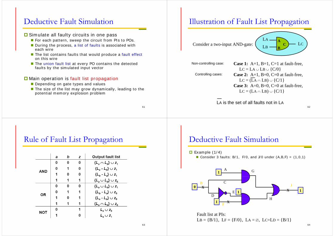
Deductive Fault Simulation Simulate all faulty circuits in one pass
For each pattern, sweep the circuit from PIs to POs. During the process, a list of faults is associated with
each wire The list contains faults that would produce a fault effect
on this wire The union fault list at every PO contains the detected
faults by the simulated input vector
Main operation is fault list propagation Depending on gate types and values The size of the list may grow dynamically, leading to the
potential memory explosion problem
62
Illustration of Fault List Propagation
Case 1: A=1, B=1, C=1 at fault-free,LC = LA LB {C/0}
Case 2: A=1, B=0, C=0 at fault-free,LC = (LA LB) {C/1}
Case 3: A=0, B=0, C=0 at fault-free,LC = (LA LB) {C/1}
Consider a two-input AND-gate:
LA is the set of all faults not in LA
A
BC
LA
LBLC
Non-controlling case:
Controlling cases:
63
Rule of Fault List Propagation
64
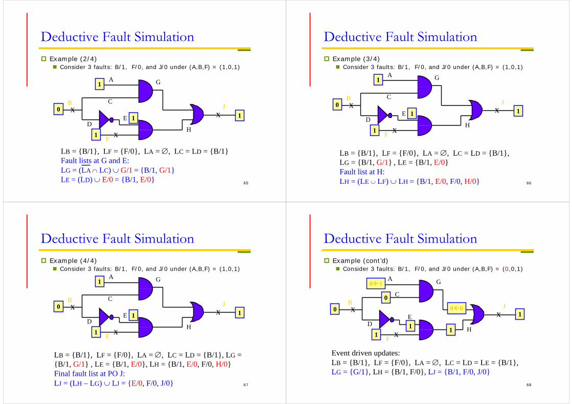
Deductive Fault Simulation Example (1/4)
Consider 3 faults: B/1, F/0, and J/0 under (A,B,F) = (1,0,1)
Fault list at PIs:LB = {B/1}, LF = {F/0}, LA = , LC=LD = {B/1}
x
x
xB C
DE
F
G
H
J
1
0
1
11
A
65
Deductive Fault Simulation Example (2/4)
Consider 3 faults: B/1, F/0, and J/0 under (A,B,F) = (1,0,1)
x
x
xB C
DE
F
G
H
J
1
0
1
11
A
LB = {B/1}, LF = {F/0}, LA = , LC = LD = {B/1}Fault lists at G and E: LG = (LA LC) G/1 = {B/1, G/1}LE = (LD) E/0 = {B/1, E/0} 66
Deductive Fault Simulation Example (3/4)
Consider 3 faults: B/1, F/0, and J/0 under (A,B,F) = (1,0,1)
x
x
xB C
DE
F
G
H
J
1
0
1
11
A
LB = {B/1}, LF = {F/0}, LA = , LC = LD = {B/1}, LG = {B/1, G/1} , LE = {B/1, E/0}Fault list at H: LH = (LE LF) LH = {B/1, E/0, F/0, H/0}
67
Deductive Fault Simulation Example (4/4)
Consider 3 faults: B/1, F/0, and J/0 under (A,B,F) = (1,0,1)
x
x
xB C
DE
F
G
H
J
1
0
1
11
A
LB = {B/1}, LF = {F/0}, LA = , LC = LD = {B/1}, LG = {B/1, G/1} , LE = {B/1, E/0}, LH = {B/1, E/0, F/0, H/0}Final fault list at PO J: LJ = (LH – LG) LJ = {E/0, F/0, J/0} 68
Deductive Fault Simulation Example (cont’d)
Consider 3 faults: B/1, F/0, and J/0 under (A,B,F) = (0,0,1)
Event driven updates:LB = {B/1}, LF = {F/0}, LA = , LC = LD = LE = {B/1}, LG = {G/1}, LH = {B/1, F/0}, LJ = {B/1, F/0, J/0}
A
x
x
xB
C
DE
F
G
H
J
01
0
1
1
1
00
1
0

69
Outline Fault Modeling
Fault Simulation
Automatic Test Pattern Generation (ATPG) Functional approach
Boolean difference Structural approach
D-algorithmPODEM
Design for Testability
70
Typical ATPG Flow 1st phase: random test pattern generation
71
Typical ATPG Flow (cont’d) 2nd phase: deterministic test pattern generation
72
Test Pattern Generation The test set T of a fault with respect to some PO z can be
computed byT(x) = z(x) z(x)
A test pattern can be fully specified or partially specified depending on whether the values of PIs are all assigned Example
abc z z
000001010011100101110111
00000111
00000100
Input vectors (1,1,0) and (1,1,-) are fully and partially specified test patterns of fault , respectively.
73
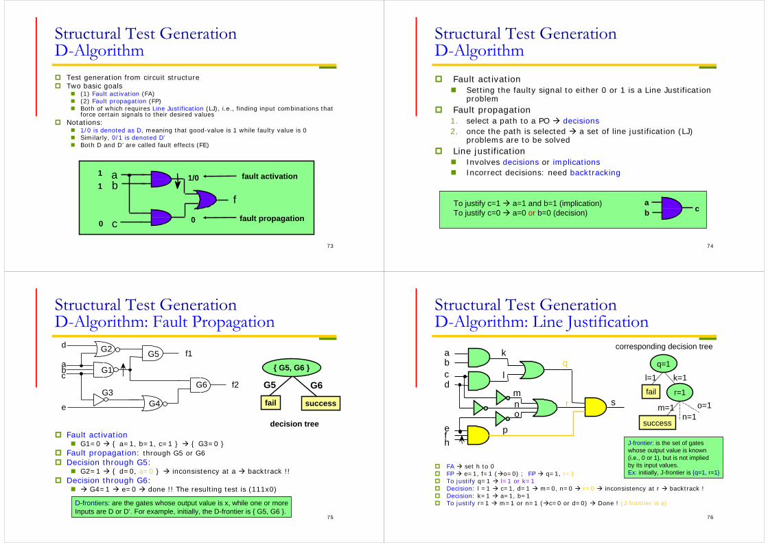
Structural Test GenerationD-Algorithm Test generation from circuit structure Two basic goals
(1) Fault activation (FA) (2) Fault propagation (FP) Both of which requires Line Justification (LJ), i.e., finding input combinations that
force certain signals to their desired values Notations:
1/0 is denoted as D, meaning that good-value is 1 while faulty value is 0 Similarly, 0/1 is denoted D’ Both D and D’ are called fault effects (FE)
fault propagation
fault activation
c
a
fb
1/0
0
11
0
74
Structural Test GenerationD-Algorithm Fault activation
Setting the faulty signal to either 0 or 1 is a Line Justification problem
Fault propagation1. select a path to a PO decisions2. once the path is selected a set of line justification (LJ)
problems are to be solved Line justification
Involves decisions or implications Incorrect decisions: need backtracking
ab cTo justify c=1 a=1 and b=1 (implication)
To justify c=0 a=0 or b=0 (decision)
75
Structural Test GenerationD-Algorithm: Fault Propagation
Fault activation G1=0 { a=1, b=1, c=1 } { G3=0 }
Fault propagation: through G5 or G6 Decision through G5:
G2=1 { d=0, a=0 } inconsistency at a backtrack !! Decision through G6:
G4=1 e=0 done !! The resulting test is (111x0)
f1
f2
G5
G6
G1
G2
G3G4
abc
d
e
G5 G6
decision tree
fail success
{ G5, G6 }
D-frontiers: are the gates whose output value is x, while one or moreInputs are D or D’. For example, initially, the D-frontier is { G5, G6 }.
76
Structural Test GenerationD-Algorithm: Line Justification
FA set h to 0 FP e=1, f=1 (o=0) ; FP q=1, r=1 To justify q=1 l=1 or k=1 Decision: l =1 c=1, d=1 m=0, n=0 r=0 inconsistency at r backtrack ! Decision: k=1 a=1, b=1 To justify r=1 m=1 or n=1 (c=0 or d=0) Done ! (J-frontier is )
abcd
efh
p
k
lq
rmno
s
corresponding decision tree
l=1 k=1
m=1 o=1n=1
J-frontier: is the set of gates whose output value is known(i.e., 0 or 1), but is not implied by its input values. Ex: initially, J-frontier is {q=1, r=1}
fail
success
q=1
r=1
77
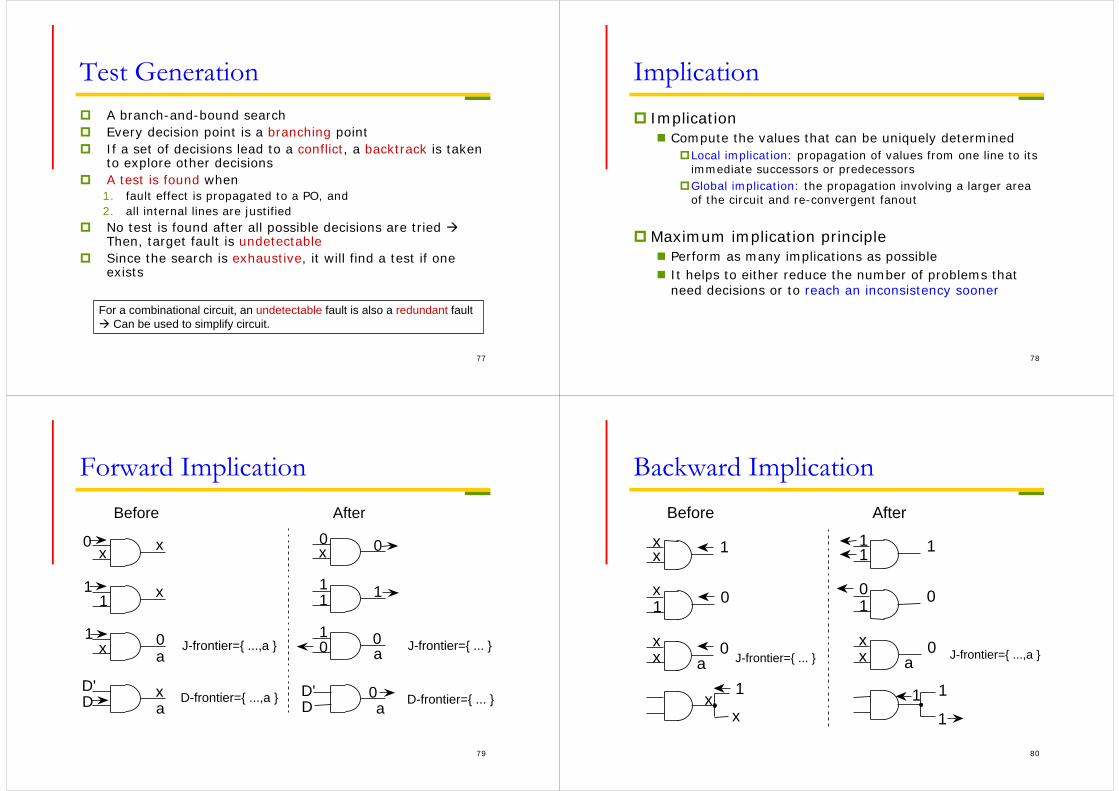
Test Generation A branch-and-bound search Every decision point is a branching point If a set of decisions lead to a conflict, a backtrack is taken
to explore other decisions A test is found when
1. fault effect is propagated to a PO, and2. all internal lines are justified
No test is found after all possible decisions are tried Then, target fault is undetectable
Since the search is exhaustive, it will find a test if one exists
For a combinational circuit, an undetectable fault is also a redundant fault Can be used to simplify circuit.
78
Implication Implication
Compute the values that can be uniquely determinedLocal implication: propagation of values from one line to its
immediate successors or predecessorsGlobal implication: the propagation involving a larger area
of the circuit and re-convergent fanout
Maximum implication principle Perform as many implications as possible It helps to either reduce the number of problems that
need decisions or to reach an inconsistency sooner
79
Forward Implication
0x
11
1x a
0
x
x
J-frontier={ ...,a }
Before
D'D a
x D-frontier={ ...,a }
0x
11
10 a
0
1
0
J-frontier={ ... }
After
D'D a
0 D-frontier={ ... }
80
Backward Implication
xx
x1
xx J-frontier={ ... }
1
0
x1
x
a0
11
01
xx a
0
0
1
J-frontier={ ...,a }
1 1
1
Before After
81
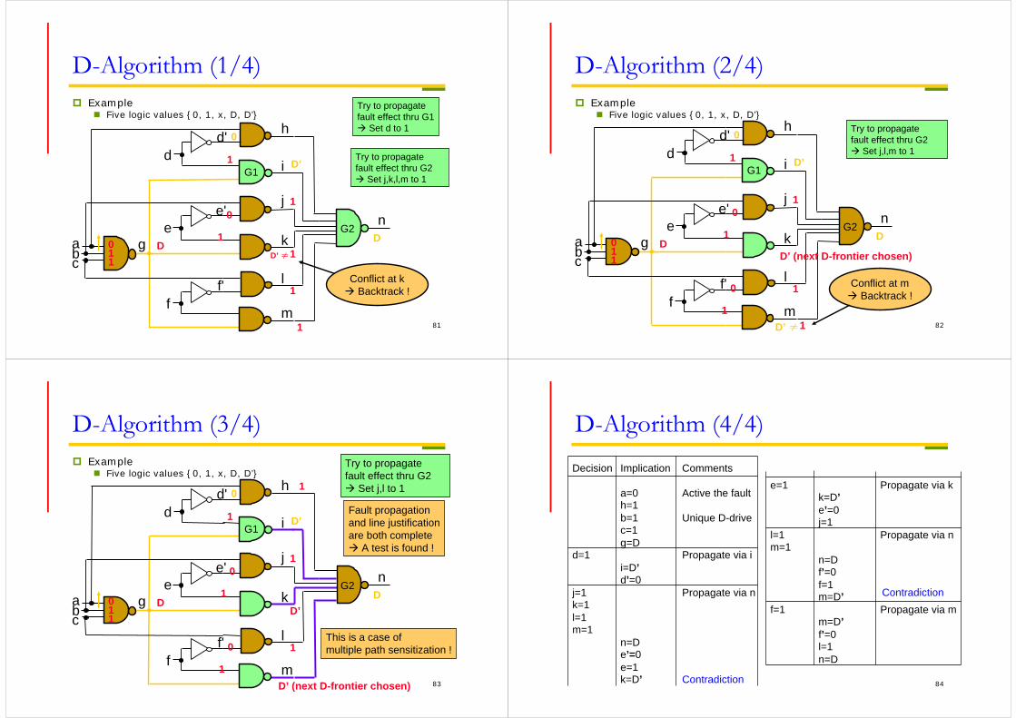
D-Algorithm (1/4) Example
Five logic values {0, 1, x, D, D’}h
Try to propagatefault effect thru G1 Set d to 1
Try to propagatefault effect thru G2 Set j,k,l,m to 1
1
1
1
1
Dn
d
e
ff'
e'
d'
i
j
k
l
m
gabc
1
0
D’G1
D011
G20
1D’ ≠
Conflict at k Backtrack !
82
D-Algorithm (2/4) Example
Five logic values {0, 1, x, D, D’}
n
d
e
ff'
e'
d'h
i
j
k
l
m
gabc
1
0
D’G1
D011
G2
1
1
1
D
0
1
0
1D’ ≠
Conflict at m Backtrack !
D’ (next D-frontier chosen)
Try to propagatefault effect thru G2 Set j,l,m to 1
83
D-Algorithm (3/4) Example
Five logic values {0, 1, x, D, D’}
n
d
e
ff'
e'
d' h
i
j
k
l
m
gabc
1
0
D’G1
D011
G2
D’
1
1
D
0
1
D’ (next D-frontier chosen)
0
1
Fault propagationand line justificationare both complete A test is found !
This is a case of multiple path sensitization !
Try to propagatefault effect thru G2 Set j,l to 11
84
D-Algorithm (4/4)Decision Implication Comments
a=0 Active the faulth=1b=1 Unique D-drivec=1g=D
d=1 Propagate via ii=D’d’=0
j=1 Propagate via nk=1l=1m=1
n=De’=0e=1k=D’ Contradiction
e=1 Propagate via kk=D’e’=0j=1
l=1 Propagate via nm=1
n=Df’=0f=1m=D’ Contradiction
f=1 Propagate via mm=D’f’=0l=1n=D
85
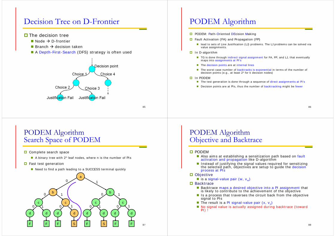
Decision Tree on D-Frontier The decision tree
Node D-frontier Branch decision taken A Depth-First-Search (DFS) strategy is often used
86
PODEM Algorithm PODEM: Path-Oriented DEcision Making
Fault Activation (FA) and Propagation (FP) lead to sets of Line Justification (LJ) problems. The LJ problems can be solved via
value assignments.
In D-algorithm TG is done through indirect signal assignment for FA, FP, and LJ, that eventually
maps into assignments at PI’s
The decision points are at internal lines
The worst-case number of backtracks is exponential in terms of the number of decision points (e.g., at least 2k for k decision nodes)
In PODEM The test generation is done through a sequence of direct assignments at PI’s
Decision points are at PIs, thus the number of backtracking might be fewer
87
PODEM AlgorithmSearch Space of PODEM Complete search space
A binary tree with 2n leaf nodes, where n is the number of PIs
Fast test generation Need to find a path leading to a SUCCESS terminal quickly
0 1
c
d
0
d
1
d
0 1
b0 1
c
d
0
d
1c
d
0
d
1
0 1
F F F F
b
c
d
a
S S F F 88
PODEM AlgorithmObjective and Backtrace PODEM
Also aims at establishing a sensitization path based on fault activation and propagation like D-algorithm
Instead of justifying the signal values required for sensitizingthe selected path, objectives are setup to guide the decision process at PIs
Objective is a signal-value pair (w, vw)
Backtrace Backtrace maps a desired objective into a PI assignment that
is likely to contribute to the achievement of the objective Is a process that traverses the circuit back from the objective
signal to PIs The result is a PI signal-value pair (x, vx) No signal value is actually assigned during backtrace (toward
PI) !

89
PODEM AlgorithmObjectiveObjective routine involves
selection of a D-frontier, G selection of an unspecified input gate of G
Objective() {/* The target fault is w s-a-v *//* Let variable obj be a signal-value pair */if (the value of w is x) obj = ( w, v’ );else {
select a gate (G) from the D-frontier;select an input (j) of G with value x;c = controlling value of G;obj = (j, c’);
}return (obj);
}
fault activation
fault propagation
90
PODEM AlgorithmBacktrace Backtrace routine involves
finding an all-x path from objective site to a PI, i.e., every signal in this path has value x
Backtrace(w, vw) {/* Maps objective into a PI assignment */G = w; /* objective node */ v = vw; /* objective value */while (G is a gate output) { /* not reached PI yet */
inv = inversion of G;select an input (j) of G with value x;G = j; /* new objective node */v = v⊕inv; /* new objective value */
}/* G is a PI */ return (G, v);
}
91
PODEM AlgorithmPI Assignment
0 1
0 1
0
b
c
d
a
S
failure
PIs: { a, b, c, d }Current Assignments: { a=0 }Decision: b=0 objective failsReverse decision: b=1Decision: c=0 objective failsReverse decision: c=1Decision: d=0
0
failureFailure means fault effect cannot be propagated to any PO under currentPI assignments
92
PODEM AlgorithmPODEM () /* using depth-first-search */
beginIf(error at PO) return(SUCCESS);
If(test not possible) return(FAILURE);
(k, vk) = Objective(); /* choose a line to be justified */
(j, vj) = Backtrace(k, vk); /* choose the PI to be assigned */
Imply (j, vj); /* make a decision */
If ( PODEM()==SUCCESS ) return (SUCCESS);
Imply (j, vj’); /* reverse decision */
If ( PODEM()==SUCCESS ) return(SUCCESS);
Imply (j, x);
Return (FAILURE);
end
93
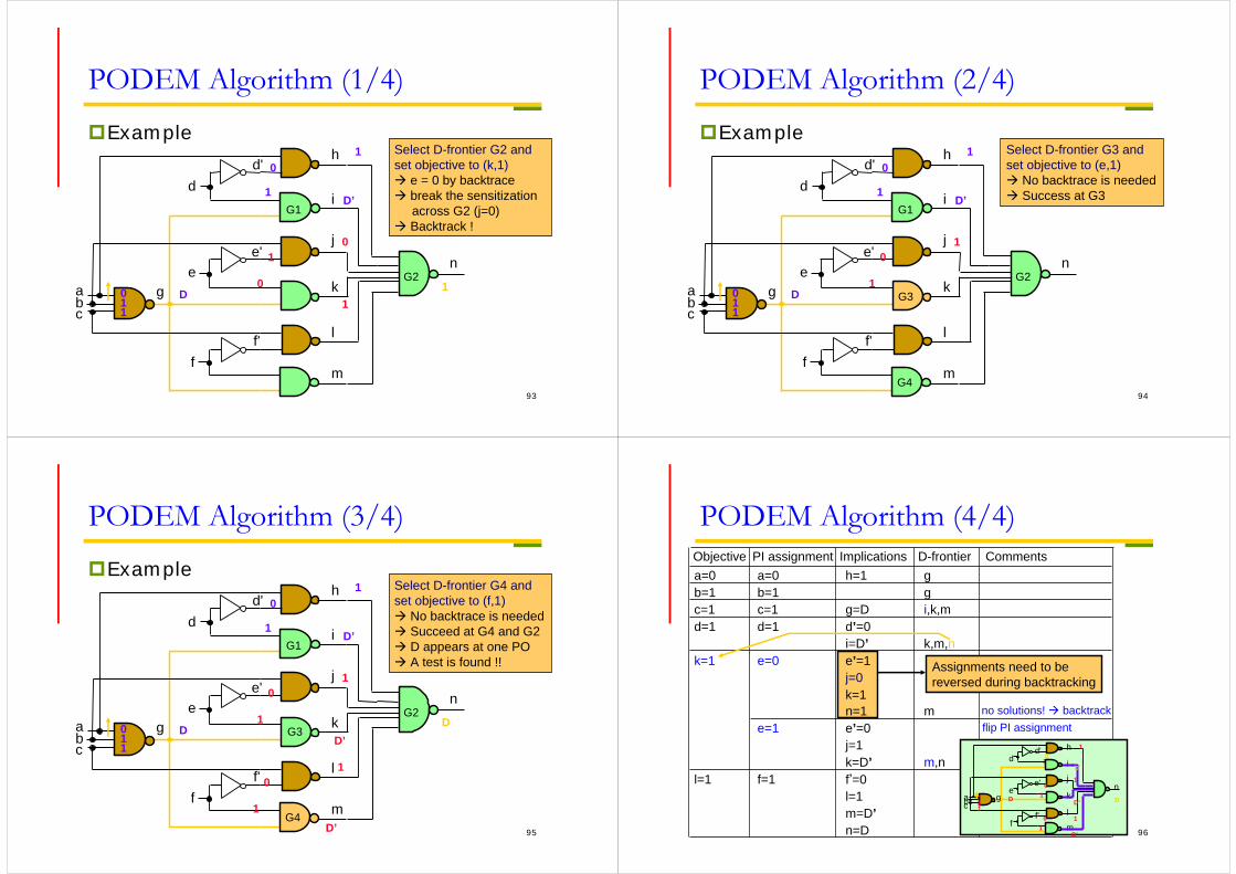
PODEM Algorithm (1/4)
Example
n
d
e
ff'
e'
d'h
i
j
k
l
m
gabc
1
0
D’G1
D011
G2
1
0
1
1
0
1 Select D-frontier G2 and set objective to (k,1) e = 0 by backtrace break the sensitization
across G2 (j=0) Backtrack !
94
PODEM Algorithm (2/4)
Example
n
d
e
ff'
e'
d'h
i
j
k
l
m
gabc
1
0
D’G1
D011
G2
1 Select D-frontier G3 and set objective to (e,1) No backtrace is needed Success at G3
G3
G4
10
1
95
PODEM Algorithm (3/4)
Example
n
d
e
ff'
e'
d'h
i
j
k
l
m
gabc
1
0
D’G1
D011
G2
1
D’D
0
1
1 Select D-frontier G4 and set objective to (f,1) No backtrace is needed Succeed at G4 and G2 D appears at one PO A test is found !!
G3
G4
10
1D’ 96
PODEM Algorithm (4/4)Objective PI assignment Implications D-frontier Commentsa=0 a=0 h=1 gb=1 b=1 gc=1 c=1 g=D i,k,md=1 d=1 d’=0
i=D’ k,m,nk=1 e=0 e’=1
j=0k=1n=1 m no solutions! backtrack
e=1 e’=0 flip PI assignmentj=1k=D’ m,n
l=1 f=1 f’=0l=1m=D’n=D
n
d
e
ff'
e'
d' h
i
j
k
l
m
gabc
10
D’
D011
1
D’
1
D
01
01
D’
1
Assignments need to bereversed during backtracking

97
PODEM AlgorithmDecision Tree Decision node:
PI selected through backtrace for value assignment Branch:
value assignment to the selected PI
a
b
c
d
e
0
0
1
1
1
f
1
fail
success 98
Termination Conditions D-algorithm
Success: (1) Fault effect at an output (D-frontier may not be empty)(2) J-frontier is empty
Failure:(1) D-frontier is empty (all possible paths are false)(2) J-frontier is not empty
PODEM Success:
Fault effect seen at an output Failure:
Every PI assignment leads to failure, in which D-frontier is empty while fault has been activated
99
PODEM Overview PODEM
examines all possible input patterns implicitly but exhaustively (branch-and-bound) for finding a test
complete like D-algorithm (i.e., will find a test if exists)
Other key features No J-frontier, since there are no values that require
justification No consistency check, as conflicts can never occur No backward implication, because values are propagated only
forward Backtracking is implicitly done by simulation rather than by an
explicit and time-consuming save/restore process Experiments show that PODEM is generally faster than D-
algorithm
100
Outline
Fault Modeling
Fault Simulation
Automatic Test Pattern Generation
Design for Testability
101
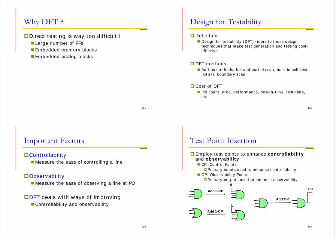
Why DFT ?
Direct testing is way too difficult ! Large number of FFs Embedded memory blocks Embedded analog blocks
102
Design for Testability Definition
Design for testability (DFT) refers to those design techniques that make test generation and testing cost-effective
DFT methods Ad-hoc methods, full and partial scan, built-in self-test
(BIST), boundary scan
Cost of DFT Pin count, area, performance, design-time, test-time,
etc.
103
Important Factors
ControllabilityMeasure the ease of controlling a line
ObservabilityMeasure the ease of observing a line at PO
DFT deals with ways of improvingControllability and observability
104
Test Point Insertion Employ test points to enhance controllability
and observability CP: Control Points
Primary inputs used to enhance controllability OP: Observability Points
Primary outputs used to enhance observability0
1
Add 0-CP
Add 1-CP
Add OP
PO
105
Control Point Insertion
Normal operation:When CP_enable = 0
Inject 0:Set CP_enable = 1 and CP = 0
Inject 1:Set CP_enable = 1 and CP = 1
C1 C2MUX0
1
CP
CP_enableInserted circuit for controlling line w
w
106
Control Point SelectionGoalControllability of the fanout-cone of the added
point is improved
Common selectionsControl, address, and data buses Enable/hold inputs Enable and read/write inputs to memoryClock and preset/clear signals of flip-flopsData select inputs to multiplexers and
demultiplexers
107
Observation Point Selection Goal
Observability of the transitive fanins of the added point is improved
Common choice Stem lines with more fanouts Global feedback paths Redundant signal lines Output of logic devices having many inputs
MUX, XOR trees Output from state devices Address, control and data buses
108
Problems with Test Point Insertion Large number of I/O pins
Can be resolved by adding MUXs to reduce the number of I/O pins, or by adding shift-registers to impose CP values
X Z
X’ Z’Shift-register R1
control Observe
Shift-register R2
109
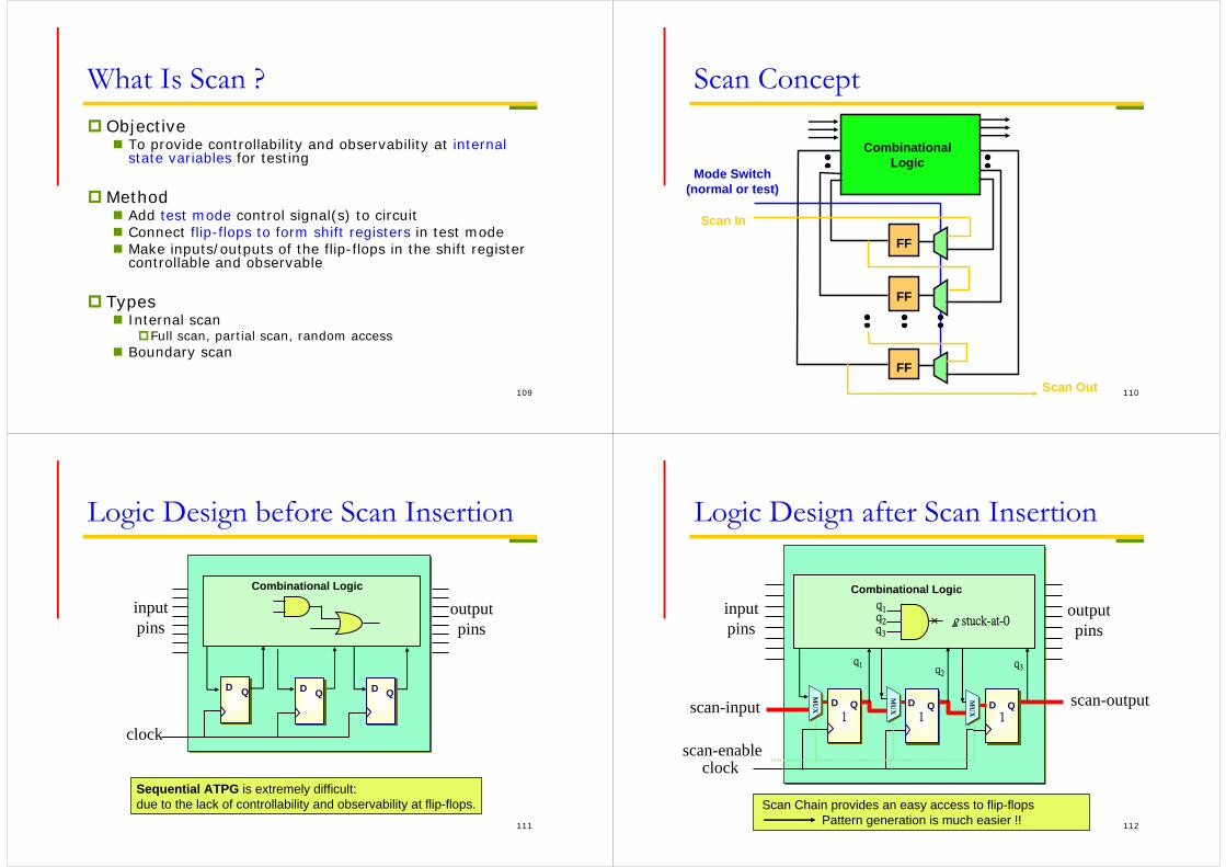
What Is Scan ?Objective
To provide controllability and observability at internal state variables for testing
Method Add test mode control signal(s) to circuit Connect flip-flops to form shift registers in test mode Make inputs/outputs of the flip-flops in the shift register
controllable and observable
Types Internal scan
Full scan, partial scan, random access Boundary scan
110
Scan Concept
CombinationalLogic
FF
FF
FF
Mode Switch(normal or test)
Scan In
Scan Out
111
Logic Design before Scan Insertion
Sequential ATPG is extremely difficult: due to the lack of controllability and observability at flip-flops.
D Q
inputpins
clock
outputpins
D Q D Q
Combinational Logic
112
Logic Design after Scan Insertion
Scan Chain provides an easy access to flip-flopsPattern generation is much easier !!
11D Q
inputpins
clock
outputpins
11D Q
11D Q
Combinational Logic
scan-input scan-outputMU
X
MU
X
MU
X
scan-enable
g stuck-at-0
q1q2q3
q1 q2q3

113
Scan Insertion Example
3-stage counter
11
D Q
inputpins
clock
outputpins
11
D Q11
D Q
Combinational Logic
q1 q2q3
g stuck-at-0
q1q2q3
It takes 8 clock cycles to set the flip-flops to be (1, 1, 1), for detecting the target fault g stuck-at-0 fault (220 cycles for a 20-stage counter !) 114
Overhead of Scan Design
Case study#CMOS gates = 2000 Fraction of flip-flops = 0.478 Fraction of normal routing = 0.471
0.9111.9%14.05%Optimized0.8716.93%14.05%Hierarchical1.000None
Normalized operating frequency
Actual area overhead
Predicted overhead
Scan implementation
115
Full Scan Problems Problems
Area overhead Possible performance degradation High test application time Power dissipation
Features of commercial tools Scan-rule violation check (e.g., DFT rule check) Scan insertion (convert a FF to its scan version) ATPG (both combinational and sequential) Scan chain reordering after layout
116
Scan-Chain Reordering Scan-chain order is often decided at gate-level without knowing
the cell placement Scan-chain consumes a lot of routing resources, and could be
minimized by re-ordering the flip-flops in the chain after layout is done
Scan-In
Scan-Out Scan-Out
Scan-In
Layout of a cell-based design A better scan-chain order
Scan cell
117
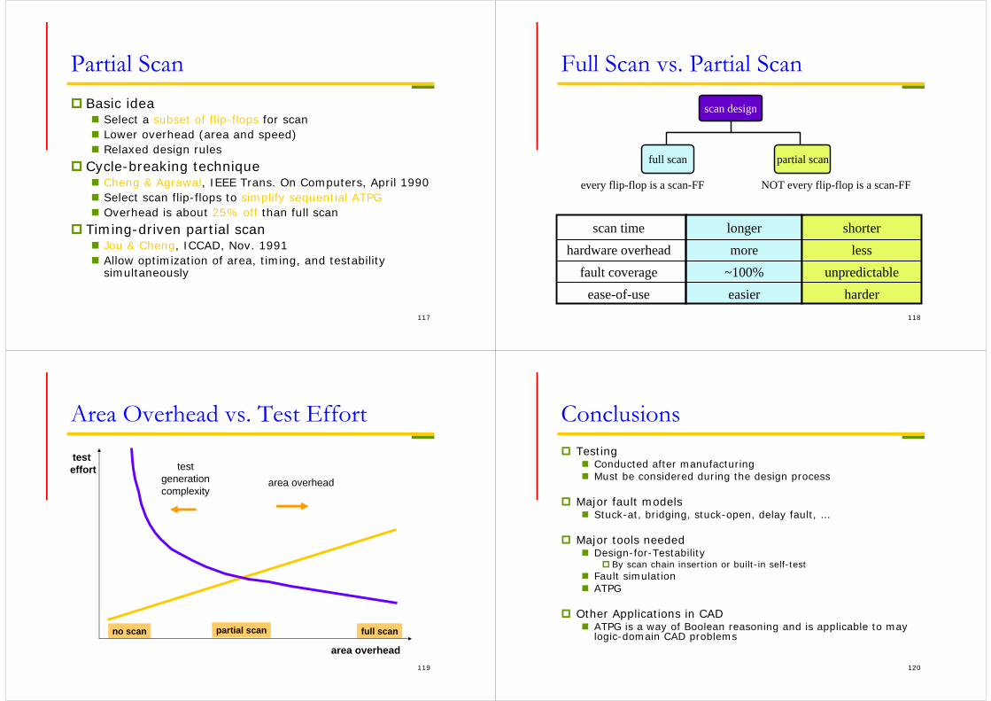
Partial Scan Basic idea
Select a subset of flip-flops for scan Lower overhead (area and speed) Relaxed design rules
Cycle-breaking technique Cheng & Agrawal, IEEE Trans. On Computers, April 1990 Select scan flip-flops to simplify sequential ATPG Overhead is about 25% off than full scan
Timing-driven partial scan Jou & Cheng, ICCAD, Nov. 1991 Allow optimization of area, timing, and testability
simultaneously
118
Full Scan vs. Partial Scan
scan design
full scan partial scan
every flip-flop is a scan-FF NOT every flip-flop is a scan-FF
scan timehardware overhead
fault coverageease-of-use
longermore
~100%easier
shorterless
unpredictableharder
119
Area Overhead vs. Test Efforttest effort
area overhead
no scan partial scan full scan
area overheadtest
generationcomplexity
120
Conclusions Testing
Conducted after manufacturing Must be considered during the design process
Major fault models Stuck-at, bridging, stuck-open, delay fault, …
Major tools needed Design-for-Testability
By scan chain insertion or built-in self-test Fault simulation ATPG
Other Applications in CAD ATPG is a way of Boolean reasoning and is applicable to may
logic-domain CAD problems