intrinsically conductive polymer
TRANSCRIPT

U.P.B. Sci. Bull., Series C, Vol. 74, Iss. 4, 2012 ISSN 1454-234x
BEHAVIOR OF ELECTRICAL STRESSED FLEXIBLE RESISITVE LAYER.
PART II: INTRINSICALLY CONDUCTIVE POLYMER
Detlef BONFERT1, Paul SVASTA2, Ciprian IONESCU3
Includerea senzorilor rezistivi în designul dispozitivelor electronice organice este necesară pentru a extinde domeniul aplicaţiilor posibile. Pentru aceasta este necesară identificarea materialelor rezistive, a proceselor şi metodelor de structurare, precum şi analiza proprietăţilor rezistive pe substrat flexibil ale acestora. Două materiale cu aplicaţie largă în electronica organică sunt polimerii umpluţi cu carbon (carbon filled polymer, CFP) şi polimerii cu conducţie intrinsecă (ICP, poly (3, 4-ethylendioxythiophene) doped with polystyrene sulfonate acid, PEDOT:PSS). Lucrarea are ca scop prezentarea comportării acestor polimeri conductivi pe suport flexibil sub influenţa curentului continuu şi în impulsuri, subliniind variaţiile rezultate ale proprietăţilor rezistive. Lucrarea este prezentată în două părţi, prima parte analizează comportarea polimerilor umpluţi cu carbon iar partea a doua pune accentul pe polimerii cu conducţie intrinsecă.
There is a necessity to include sensors (resistors) in the design of organic electronic devices in order to extend the range of possible applications. It is essential to identify potential resistive materials, the processes and methods to structure them and to analyze their resistive properties on flexible substrates. Two materials widely used in organic electronics are carbon filled polymer (CFP) and the intrinsically conductive polymer (ICP) poly (3, 4-ethylendioxythiophene) doped with polystyrene sulfonate acid (PEDOT:PSS). In this paper we focus on the DC and pulsed stress behavior of these conductive polymers on flexible substrates and the resulting changes of their resistive properties. The paper is presented in two parts. Part one deals with carbon filled polymers (CFPs)and part two analyzes the behavior of intrinsically conductive polymesrs (ICPs).
Keywords: Thick Film Flexible Resistors, Carbon filled polymer, PEDOT:PSS, DC- and Pulsed Stress
1 Researcher, Polytronics Dept., Fraunhofer EMFT, Munich, Germany, e-mail:
[email protected] 2 Prof., Electronics Faculty, CETTI, University POLITEHNICA of Bucharest, Romania, e-mail:
[email protected] 3 Reder, Electronics Faculty, CETTI, University POLITEHNICA of Bucharest, Romania, e-mail:
124 Detlef Bonfert, Paul Svasta, Ciprian Ionescu
NOTE The first part of the paper analyzed the behavior of electrical stressed carbon
filled polymesrs (CFPs): - Part I: Carbon Filled Polymer. This part was published in the previous issue of the Scientific Bulletin of UPB.
1. Intrinsically conductive polymer layer
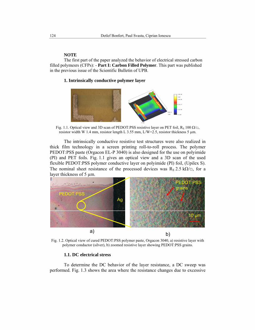
Fig. 1.1. Optical view and 3D scan of PEDOT:PSS resistive layer on PET foil, RS 100 Ω/□,
resistor width W 1.4 mm, resistor length L 3.55 mm, L/W=2.5, resistor thickness 5 µm.
The intrinsically conductive resistive test structures were also realized in thick film technology in a screen printing roll-to-roll process. The polymer PEDOT:PSS paste (Orgacon EL-P 3040) is also designed for the use on polyimide (PI) and PET foils. Fig. 1.1 gives an optical view and a 3D scan of the used flexible PEDOT:PSS polymer conductive layer on polyimide (PI) foil, (Upilex S). The nominal sheet resistance of the processed devices was RS 2.5 kΩ/□, for a layer thickness of 5 µm.
10 µm
a) b)
Ag
PEDOT:PSS grains
PEDOT:PSS
Fig. 1.2. Optical view of cured PEDOT:PSS polymer paste, Orgacon 3040, a) resistive layer with
polymer conductor (silver), b) zoomed resistive layer showing PEDOT:PSS grains.
1.1. DC electrical stress
To determine the DC behavior of the layer resistance, a DC sweep was performed. Fig. 1.3 shows the area where the resistance changes due to excessive

Behavior of electrical stressed […]. Part II: Intrinsically conductive polymer 125
voltage rating outside the normal operating values. The resistor is heated up and the resistance decreases because of the negative TCR of the polymer material.
Between pulsing, the DC spot measurement was set in the safe operating area to 0.1 mA.
PEDOT:PSS Resistor , (Tempered 105°C 2h,)Double Current Sweep 0-1mA, R01, PET Foil 1
0.0
1.0
2.0
3.0
4.0
5.0
6.0
7.0
0.0 0.1 0.2 0.3 0.4 0.5 0.6 0.7 0.8 0.9 1.0
Current / mA
Volta
ge /
V
6.20
6.22
6.24
6.26
6.28
6.30
Res
ista
nce
/ kΩ
VoltageResistance
Fig. 1.3. DC resistance during current sweep, PEDOT:PSS resistive layer on PET foil,
RS 2.5 kΩ/□ (reversible changes).
a) b)
PEDOT:PSS Resistor , (Temp.105°C 2h,),Curr. Sampling 0.1 - 2.0 mA, R01, PET Foil 1, Meas. 9-14
6300
6350
6400
6450
6500
6550
0 2 4 6 8 10 12 14 16 18 20 22 24Time / s
R / Ω
T1 = 26 °C T2 = 28 °C
T3 = 30 °CT4 = 38 °C
T5 = 49 °C
T6 = 65 °C
Ih = 0.5 mAIh = 1.0 mA
Ih = 1.5 mA
Ih = 2 mA
Ih = 0.1 mA Ih = 0.2 mA
RDC, PEDOT:PSS Layer, Tempered, Current Sampling, 0.1-5mA, R13, PET Foil 1, M2-M10
4150
4200
4250
4300
4350
4400
4450
0 2 4 6 8 10 12 14 16 18 20 22 24Time / s
R4P
-K / Ω
0.1mA0.5mA1.0mA2.0mA3.0mA4.0mA5.0mA0.1mAb
1.0mA
0.5mA
5.0mA
0.1mA a
0.1mA b
2.0mA
4.0mA 3.0mA
Fig. 1.4. DC resistance during current sampling, PEDOT:PSS resistive layer on PET foil,
a) reversible changes, b) irreversible changes.
Fig. 1.5.Temperature distribution during self- heating of PEDOT:PSS resistive layer on PET foil,
hot spot in the center of the resistive layer.
126 Detlef Bonfert, Paul Svasta, Ciprian Ionescu
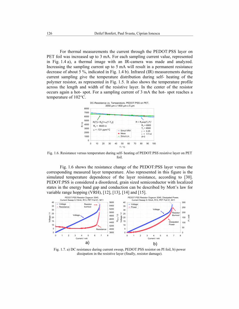
For thermal measurements the current through the PEDOT:PSS layer on PET foil was increased up to 3 mA. For each sampling current value, represented in Fig. 1.4 a), a thermal image with an IR-camera was made and analyzed. Increasing the sampling current up to 5 mA will result in a permanent resistance decrease of about 5 %, indicated in Fig. 1.4 b). Infrared (IR) measurements during current sampling give the temperature distribution during self- heating of the polymer resistor, as represented in Fig. 1.5. It also shows the temperature profile across the length and width of the resistive layer. In the center of the resistor occurs again a hot- spot. For a sampling current of 3 mA the hot- spot reaches a temperature of 102°C.
DC-Resistance vs. Temperature, PEDOT:PSS on PET, 3550 µm x 1400 µm x 5 µm
0
1000
2000
3000
4000
5000
6000
7000
8000
0 10 20 30 40 50 60 70 80 90 100T / °C
R / Ω
Simul-VRHMeasSimul-Lin
R = Roexp(To/T)γ
Ro = 6900To = 6500γ = 0.25γ = 1/1+dd=3
R(T)= R0[1+α(T-T0)]
R0 = 6620 Ωα = -721 ppm/°C
Fig. 1.6. Resistance versus temperature during self- heating of PEDOT:PSS resistive layer on PET
foil. Fig. 1.6 shows the resistance change of the PEDOT:PSS layer versus the
corresponding measured layer temperature. Also represented in this figure is the simulated temperature dependence of the layer resistance, according to [30]. PEDOT:PSS is considered a disordered, grain sized semiconductor with localized states in the energy band gap and conduction can be described by Mott’s law for variable range hopping (VRH), [12], [13], [14] and [15].
a) b)
PEDOT:PSS Resistor Orgacon 3040, Current Sweep 0-10mA, R13, PET Foil 01, M11
0
5
10
15
20
25
30
35
40
0 1 2 3 4 5 6 7 8Current / mA
Volta
ge /
V
3800400042004400460048005000520054005600
R4P
-K / Ω
VoltageResistance
Voltage
Resistance
Resistorburnout
PEDOT:PSS Resistor Orgacon 3040, Dissipated Power,Current Sweep 0-10mA, R13, PET Foil 01, M11
0
5
10
15
20
25
30
35
40
0 1 2 3 4 5 6 7 8Current / mA
Volta
ge /
V
0
50
100
150
200
250
300
P / m
W
VoltagePower
ResistorBurnout
DissipatedPower
Voltage
Fig. 1.7. a) DC resistance during current sweep, PEDOT:PSS resistor on PI foil, b) power
dissipation in the resistive layer (finally, resistor damage).

Behavior of electrical stressed […]. Part II: Intrinsically conductive polymer 127
Applying a current sweep up to 7 mA, as represented in Fig. 1.7 a), will finally lead to the burn- out of the resistive layer in the area of the hot spot. The dissipated power during burn out, shown in Fig. 1.7 b) reaches 0.25 W, corresponding to a power density of 5 W/cm2 of resistive area, which is less than the corresponding value of the carbon based resistor. Fig. 1.8 shows the burn out region in the center of the resistive layer. Because of the excessive heat the substrate PET foil is melted under the resistive layer. The image also reveals the straight cut across the resistors width in this area. Similar characteristic damage of DC- stressed resistive layer is presented in [34].
a) b)
Resistor burnout
Fig. 1.8. a) Resistor burnout during DC stressing, b) caused by hot spot in the center of the flexible
polymer PEDOT:PSS resistor on PET foil.
1.2 Pulsed electrical stress
The behavior of the PEDOT:PSS resistive layer during pulsed stress was studied applying 100 ns wide pulses from transmission line pulser with increasing and constant amplitudes.
1.2.1 Influence of pulse amplitude on resistance
To determine the influence of pulse amplitude on the resistance, TLP measurements were performed, similar to those on carbon based resistors, with stepwise increasing the open source TLP pulse amplitudes. Recording the measured voltage and current transients at the polymer layer during each voltage step, gives a 3D representation of the measurement, as shown in Fig. 1.9.

128 Detlef Bonfert, Paul Svasta, Ciprian Ionescu
Time
P1
Pulse
num
ber
Pulse amplitude
P2P3
Pn
Fig. 1.9. 3D representation of a) pulsed voltage at and b) pulsed current through the PEDOT:PSS
resistive layer on PET foil, for TLP pulse width of 100 ns, TLP-voltage 0-1000 V, 2 V step.
Transient Voltage and Current at DUT, TLP 100 ns, 900V, PEDOT:PSS on PET Foil 1, R13, 1300Ω/□, M1
-1000
100200300400500600700800
-20 0 20 40 60 80 100 120Time / ns
Pul
sed
Vol
tage
/V
-0.30.00.30.50.81.01.31.51.82.0
Pul
sed
Cur
rent
/ A
Pulsed current
Pulsed voltage
Fig. 1.10. Pulsed voltageat and pulsed current through PEDOT:PSS resistive layer on PET foil for
TLP pulse width of 100 ns, TLP-voltage 900 V.
Rpulsed , TLP 100 ns, 100 V and 900 V, PEDOT:PSS on PET Foil 1, R13, 1300Ω/□, M1
2500
3000
3500
4000
4500
20 30 40 50 60 70 80 90 100Time / ns
Pul
sed
Res
ista
nce
/ Ω
TlpRes_900V_TlpTlpRes_100V_Tlp
Calculated resistance during stress pulseTLP 900 V
TLP 100 V
Fig. 1.11. Pulsed resistance of PEDOT:PSS resistive layer on PET foil for TLP pulse width of
100 ns, TLP-voltage 100 V and 900 V.

Behavior of electrical stressed […]. Part II: Intrinsically conductive polymer 129
During the pulses, the pulsed resistance is calculated from each corresponding point of the current- and voltage transients, represented in Fig. 1.10. Fig. 1.11 shows the pulsed resistance for two TLP voltages, 100 V to 900 V. The resistance decreases with increasing TLP voltage due to Joule heating during the pulse and of the negative TCR of the material.
1.2.2 Influence of successive pulsing on resistance
Fig. 1.12 depicts the pulsed current-voltage characteristic for four successive measurements, M1 – M4. During each measurement the amplitude of the 100 ns wide pulses was stepwise increased, in 2 V steps, up to 1000 V of the TLP charging voltage. The different shapes of these characteristics indicate permanent and reversible changes that take place in the resistor during pulsing. This is confirmed by the absolute DC- resistance changes shown in Fig. 1.13 and Fig. 1.14, and by the pulsed resistance changes of Fig. 1.15.
Pulsed I-V, TLP 100 ns, 2-1000V, step 2V, PEDOT:PSS layer on PET Foil 1, R 1300Ω/□, temp. R13, M1-M4
0.0
0.1
0.1
0.2
0.2
0.3
0 100 200 300 400 500 600 700Pulsed Voltage at DUT / V
Pul
sed
Cur
rent
/ A
M1M2M3M4
Fig. 1.12. Pulsed current-voltage characteristic of PEDOT:PSS resistive layer on PET foil for
successive measurements, pulse width 100 ns. RDC, TLP 100 ns, 2-1000V, step 2V, PEDOT:PSS layer on
PET Foil 1, R13 1300Ω/□, temp., M1-M4
3345
3350
3355
3360
3365
3370
0 100 200 300 400 500 600 700Pulsed Voltage at DUT / V
DC
Res
ista
nce
/ Ω
M1
M2
M4
M3
Fig. 1.13. DC-resistance change versus applied pulse voltage for successive measurements of
PEDOT:PSS resistive layer on PET foil, pulse width 100 ns.

130 Detlef Bonfert, Paul Svasta, Ciprian Ionescu
RDC, PEDOT:PSS layer on PET Foil 1, R13 1300Ω/□, temp., M1-M3, before and after pulsing TLP 100 ns
3340
3350
3360
3370
3380
3390
3400
0 50 100 150 200 250 300 350 400 450 500V / mV
RD
C / Ω
R-M1-preR-M1-pstR-M2-pstR-M3-pst
before TLP M1
after TLP M1
after TLP M2 after TLP M3
Fig. 1.14. DC-resistance change versus applied DC voltage for successive measurements of
PEDOT:PSS resistive layer on PET foil, before and after pulsed measurements M1-M3, pulse width 100 ns, pulse voltage 2-1000V, step 2 V.
The final value of a measurement is the starting value for the following
one, indicating irreversible changes in the resistor material.
Rpulsed, TLP 100 ns, 2-1000V, step 2V, PEDOT:PSS layer on PET Foil 1, R13, 1300Ω/□, temp., M1-M4
3000
3100
3200
3300
3400
3500
0 100 200 300 400 500 600 700Pulsed Voltage at DUT / V
Pul
sed
Res
ista
nce
/ Ω
M1M2M3M4
Fig. 1.15. Pulsed resistance change versus applied pulse voltage for successive measurements of
PEDOT:PSS resistive layer on PET foil, pulse width 100 ns.
1.2.3 Influence of pulse number on resistance
Applying multiple high voltage pulses, below the breakdown value, and with constant amplitude gives information about the robustness of the resistor to the TLP stress. Up to 4000 pulses of 850 V amplitude were applied with 100 ns wide pulses, as can be seen from Fig. 1.16, for the applied first 1000 pulses. During the 100 ns pulses there is little change in voltage and current during transients, while sweeping the pulse amplitude, as shown in Fig. 1.17. The corresponding DC- and pulsed resistance during the applied number of 4000 pulses is depicted in Fig. 1.18 and Fig. 1.19, respectively, indicating a constant behavior of the intrinsic polymer layer.

Behavior of electrical stressed […]. Part II: Intrinsically conductive polymer 131
a) b)Time
Pulse
num
ber
Pulse amplitude
P1P2
P3
Pn
Fig. 1.16. 3D representation of a) pulsed voltage at and b) pulsed current through the PEDOT:PSS
resistive layer on PET foil, for TLP pulse width of 100 ns, constant TLP-voltage of 850 V, first 1000 pulses applied.
Transient Voltage and Current at DUT, TLP 100 ns, 850V,
PEDOT:PSS on PET Foil 1, R13, 1300Ω/□, M1
-1000
100200300400500600700800
-20 0 20 40 60 80 100 120Time / ns
Pul
sed
Vol
tage
/V
-0.30.00.30.50.81.01.31.51.82.0
Pul
sed
Cur
rent
/ A
Pulsed current
Pulsed voltage
Fig. 1.17. Pulsed voltage at and pulsed current through PEDOT:PSS resistive layer on PET foil for
TLP pulse width of 100 ns, constant TLP-voltage 850 V.
RDC, TLP 100ns, 850V, 4000 Pulses, PEDOT:PSS layer on PET Foil 1, R13 1300 Ω/□, temp., M1
RDC = -5E-05n + 3597.8
3585
3590
3595
3600
3605
0 500 1000 1500 2000 2500 3000 3500 4000Number of Voltage Pulses at DUT / #
DC
Res
ista
nce
/ Ω
MeasLinear (Meas)
Fig. 1.18. DC-resistance change versus number of applied pulses with constant voltage, TLP -
voltage 850V, pulse width 100 ns, 4000 applied pulses.

132 Detlef Bonfert, Paul Svasta, Ciprian Ionescu
Rpulsed, TLP 100ns, 850V, 4000 Pulses, PEDOT:PSS layer on PET Foil 1, R13,1300 Ω/□, temp., M1
Rpulsed = 6.8173E-04xn + 3.4529E+033450
3475
3500
3525
3550
0 500 1000 1500 2000 2500 3000 3500 4000Number of Voltage Pulses at DUT / #
Rpu
lsed
/ Ω
MeasLinear (Meas)
Fig. 1.19. Pulsed resistance change versus number of applied pulses with constant voltage, TLP -
voltage 850V, pulse width 100 ns, 4000 applied pulses.
2. Conclusions
We have analyzed in part one of the paper the flexible carbon based polymer thick film resistors and in part two the intrinsically conductive polymer PEDOT:PSS layer, during DC- stress, single and multiple pulse stresses, showing the behavior before, during and after the stress.
An applied DC- stress outside the safe operating area (SOA) can change the electrical properties of the layer permanently, by changing the physical structure of the resistive layer. The thermal simulation and the corresponding IR measurements revealed a hot spot in the center of the resistor, due to the low thermal conductivity of the flexible substrate. Increasing further the DC- stress, this hot spot will be the starting point of the resistors burn out, leading finally to a cut through the whole resistor width.
The high current-voltage behavior of flexible thick film polymer resistors on polyimide foil has been investigated by means of rectangular TLP pulses. The amount of resistance change depends on pulse amplitude as well as on the number of applied pulses.
The measurements show, that for the flexible thick film resistors, the resistance decreases with increasing pulse voltage. Multiple pulsing reduces this effect. Pulsing with constant amplitude produces also a decrease, but continuing pulsing stabilizes the resistance. Intrinsically conductive polymer PEDOT:PSS layer show little changes during this stress test, the resistance stabilizes from the very beginning.
The tested flexible thick film polymer resistors are susceptible to high energy pulses and this can lead to irreversible changes in the resistor and its value. Nevertheless the effects are saturating leading to more stable resistors.

Behavior of electrical stressed […]. Part II: Intrinsically conductive polymer 133
R E F E R E N C E S
[1] J. Huang, “Carbon Black Filled Conducting Polymers and Polymer Blends”, Wiley, Advances in Polymer Technology, Vol. 21, No. 4, 2002, pp. 299-313.
[2] I. Balberg, “A comprehensive picture of the electrical phenomena in carbon black-polymer composites”, Pergamon, Carbon, Vol. 40, 2002, pp. 139-143.
[3] L. C. Costa, F. Henry, “DC electrical conductivity of carbon black polymer composites at low temperatures”, Elsevier, J. of Non-Crystalline Solids, Vol. 357, 2011, pp. 1741-1744.
[4] R. Hulkkonen, E. Jarvinen, V. Sortti “Experience with Polymer Thick Film Technology”, Gordon and Breach Science Publishers, Electrocomponent Science and Technology, Vol. 10, 1983, pp. 135-141.
[5] L. B.,Groenendaal, F. Jonas, D. Freitag, H. Pielartzik, and J.R. Reynolds, “Poly(3,4-ethylenedioxy-thiophene) and Its Derivatives: Past, Present, and Future”, Wiley, Advanced Materials, Vol. 12, No. 7, 2000, pp. 481 – 494.
[6] Kirchmeyer, S. and Reuter K., “Scientific importance, properties and growing applications of poly(3,4-ethylendioxythiophene)”, RSC, J. Mater. Chem, Vol. 15, 2005, pp. 2077-2088.
[7] J. Huang, “Influence of thermal treatment on the conductivity and morphology of PEDOT:PSS films”, Elsevier, Synthetic Metals, Vol. 139, 2003, pp. 569-572.
[8] S. Meskers, J. van Duren, R. Janssen, F. Louwert, and L. B. Groenendaal, “Infrared Detectors with PEDOT:PSS as Active Material”, Wiley-VCH, Adv. Mater., Vol. 15, Nr. 7-8, 2003, pp. 613-616.
[9] I. W. Kwon, H. J. Son, W. Y. Kim, Y. S. Lee, H. C. Lee, “Thermistor behavior of PEDOT:PSS thin film”, Elsevier, Synthetic Metals, Vol. 159, 2009, pp. 1174-1177.
[10] U. Lang, N. Naujoks, J. Dual, “Mechanical characterization of PEDOT:PSS thin films”, Elsevier, Synthetic Metals, Vol. 159, 2009, pp. 473-479.
[11] H. Okuzaki, H. Suzuki, and T. Ito, “Electrically driven PEDOT:PSS actuators”, Elsevier, Synthetic Metals, Vol. 159, No. 21-22, 2009, pp. 2233-2236.
[12] Y. Taketa and M.Haradome, “Thick Film Resistors with Improved Voltage Stability”, IEEE Trans-PHP, Vol. PHP-10, No. 1, March 1974, pp. 74-81.
[13] H. Domingos, and D. C. Wunsch, “High Pulse Power Failure of Discrete Resistors”, IEEE Trans-PHP, Vol. PHP-11, No. 3 (1975), pp. 225-229.
[14] E. H. Stevens, D. A. Gilbert, and J. A. Ringo “High Voltage Damage and Low-Frequency Noise in Thick-Film Resistors”, IEEE Trans-PHP, Vol. PHP-12, No. 4 (1976), pp. 351-356.
[15] Wunsch, D.C, “An Overview of EOS Effects on Passive Components” 3rd EOS/ESD Symposium Proceedings, 1981, pp 167-173.
[16] H. Gieser, M. Haunschild “Very-Fast Transmission Line Pulsing of Integrated Structures and the Charged Device Model”, EOS/ESD Symposium Proceedings, 1996, pp 85-94.
[17] R. A. Ashton, “Transmission Line Pulse Measurements: A Tool for Development ESD Robust Integrated Circuits”, IEEE ICMTS, March 2004, pp. 1-6.
[18] S. H. Voldman, R. Ashton, J. Barth, et al, “Standardization of the Transmission Line Pulse (TLP) Methodology for Electrostatic Discharge (ESD)”, EOS/ESD Symposium Proceedings, 2003, pp. 1-10.
[19] D. Bonfert, H. Wolf, H. Gieser, A. Stocker, “ESD Susceptibility of Thick Film Resistors by Means of Transmission Line Pulsing”, IEEE ESTC, Symposium Proceedings , Dresden, Sept. 5. – 7., 2006.
[20] D. Bonfert, H. Wolf, H. Gieser, P. Svasta, A. Romanescu, and E. Cazacu, “Transmission Line Pulse Stress on Thick Film Resistors”, IEEE ISSE, Symposium Proceedings , Cluj-Napoca, May 9. – 13., 2007.

134 Detlef Bonfert, Paul Svasta, Ciprian Ionescu
[21] R. Ashton, L. Lescouzeres., “Characterization of Off Chip ESD Protection Devices” EOS/ESD Symposium Proceedings, 2008, pp. 21-29.
[22] C. S. Sangeeth, M. Jaiswal, R. Menon, “Charge Transport in Transparent Conductors: A Comparison” Journal of Applied Physics Vol. 105, 2009, pp. 063713_1-6.
[23] S. Ashizawa, R. Horikawa, H. Okuzaki, “Effects of Solvents on Carrier Transport in Poly(3, 4-ethylenedioxythiophene) / Poly (4-styrenesulfonate)” Synthetic Metals, Vol. 153, 2005, pp. 5-8.
[24] S. Meskers, K. J. van Duren, R. Janssen, “Non-linearity in the I-V characteristic of PEDOT:PSS due to Joule heating”, Elsevier, Organic electronics, Vol. 5, 2004, pp. 207-211.
[25] E. Vitoratos, E., S. Sakkopoulos, E. Dalas, N. Paliatsas, et. al, “Thermal degradation mechanism of PEDOT:PSS”, Elsevier, Organic Electronics, Vol. 10, 2009, pp. 61-66.
[26] A. Dziedzic, J. Kita, P. Mach, “Voltage nonlinearity of carbon black/polyesterimide thick resistive films”, Elsevier, Vacuum, Vol. 50, No. 1-2, 1998, pp. 125-130.
[27] T.B. Narayana, K. Ramkumar, M. Satyam, “Mechanism for downward trimming of polymer resistors”, J. of Applied Physics, Vol. 25, 1992, pp. 717-721.
[28] J. Nicolics, M. Mündlein, G. Hanreich, A. Zluc, H. Stahr, M. Franz, “Thermal Analysis of Multilayer Printed Circuit Boards with Embedded Carbon Black-Polymer Resistors”, IEEE 30th ISSE, 2007, pp. 46-52.
[29] D. Ortolino, J. Kita, R. Wurm, E. Blum, K. Beart, R. Moos, “Investigation of the short-time high-current behavior of vias manufactured in hybrid thick-film technology”, Elsevier, Microelectronics Reliability, Vol. 51, No. 7, July 2011, pp. 1257-1263.
[30] J. Ouyang, et al., “Mechanism of Conductivity Enhancement in PEDOT:PSS Film through Solvent treatment”, Elsevier, Polymer, Vol. 45, 2004, pp. 8443 – 8450.
[31] N. D. Sankir, “Selective deposition of PEDOT/PSS on to flexible substrates and tailoring the electrical resistivity by post treatment”, Emerald Group, Circuit World, Vol. 34, No. 4, 2008, pp. 32-37.
[32] Y. Srinivasa Rao, M. Satyam, “Dielectrophoretic mechanism for downward trimming of polymer resistors”, Emerald Group, Microelectronics International, Vol. 20, No. 2, 2003, pp. 10-15.
[33] Y. Srinivasa Rao, “Studies on temperature coefficient of resistance (TCR) of polymer thick film resistors”, Emerald Group, Microelectronics International, Vol. 25, No. 3, 2008, pp. 33-36.
[34] R. R. Brynsvold, K. Manning, “Constant- Current Stressing of SiCr- Based Thin- Film Resistors: Initial “Wearout” Investigations”, IEEE Trans. Device and Materials Reliability, Vol. 7, No. 2, June 2007, pp. 259-269.
[35] G. C. Psarras, “Charge Transport Properties in Carbon Black/Polymer Composites”, J. of Polymer Science: Part B: Polymer Physics, Vol. 45, 2007, pp. 2535-2545.