integrated nanophotsdonic devices micro and nano technologies
DESCRIPTION
dsdsgTRANSCRIPT

Integrated Nanophotonic Devices

Integrated Nanophotonic Devices
Zeev Zalevsky and Ibrahim Abdulhalim
Amsterdam • Boston • Heidelberg • London • New York • Oxford • Paris San Diego • San Francisco • Singapore • Sydney • Tokyo
William Andrew is an imprint of Elsevier

William Andrew is an imprint of ElsevierThe Boulevard, Langford Lane, Kidlington, Oxford OX5 1GB, UK30 Corporate Drive, Suite 400, Burlington, MA 01803, USA
Copyright © 2010 Elsevier Inc. All rights reserved
No part of this publication may be reproduced, stored in a retrieval system or transmitted in any form or by any means electronic, mechanical, photocopying, recording or otherwise without the prior written permission of the publisher
Permissions may be sought directly from Elsevier’s Science & Technology Rights Department in Oxford, UK: phone (44) (0) 1865 843830; fax (44) (0) 1865 853333; email: [email protected]. Alternatively you can submit your request online by visiting the Elsevier web site at http://elsevier.com/locate/permissions, and selecting Obtaining permission to use Elsevier material
NoticeNo responsibility is assumed by the publisher for any injury and/or damage to persons or property as a matter of products liability, negligence or otherwise, or from any use or operation of any methods, products, instructions or ideas contained in the material herein. Because of rapid advances in the medical sciences, in particular, independent verification of diagnoses and drug dosages should be made
British Library Cataloguing-in-Publication DataA catalogue record for this book is available from the British Library
Library of Congress Cataloging-in-Publication DataA catalog record for this book is availabe from the Library of Congress
ISBN: 978-1-4377-7848-9
For information on all William Andrew publications visit our web site at www.elsevierdirect.com
Printed and bound in the UK
10 11 12 13 14 10 9 8 7 6 5 4 3 2 1

xi
Preface
“I didn’t have time to write you a short letter so I wrote you a long one”Mark Twain
Nanophotonics is a newly developing and exciting field, with two main areas of interest: imaging/vision and devices for sensing and information transport. By nanophotonics one usually refers to the science and devices involving structures with sub-micron dimensions (specifically less than 100 nm) and which are interacting with photons. The disciplines developed in the field of nanophotonics have far-reaching influences in both private and public sectors, with potential applications ranging from faster computing power and “smart” eyeglasses, to national safety, security and medical applications. The recent advances in the field of nanotechnology allow realization of photonic principles and devices that previously could only be theoretically investigated. The advances in the computing capabilities allow accurate design of such devices before applying the available fabrication process. The diversity of this field is so large that a multidisciplinary research activity involving scientists from the fields of physics, material science, electro-optical engineering, process engineering and bio-physics is rapidly emerging.
One of the major nanophotonic fields of interest is related to realization of nano-integrated photonic modulation devices and sensors. The attempt to integrate photonic dynamic devices with microelectronic circuits is becoming a major scientific as well as industrial trend due to the fact that currently processing is mainly done with microelectronic chips but transmission, especially for long distances, is done over optical links. In addition, photonic processing can resolve several bottle necks generated in dense microelectronic chips, especially when going to high operation frequencies. Such bottlenecks include power dissipation problems, cross-talk problems, etc. This book will present the recent progress in designing, fabricating and experimenting integrated photonic modulation circuits. Due to the recent leap in the development of nanotechnology fabrication capabilities, the field of inte-grated nano- and microphotonic devices has significantly changed during the last few years.
In this book, which is aimed at the reading audience of graduate students in exact sciences as well as researchers in academy and industry, presents an up-to-date as well as a comprehensive and wide-range perspective of existing photonic modulation technologies including several novel approaches that were only recently developed. The book starts by giving the theoretical background of the physi-cal fundamentals that need to be known in order to follow the technical concepts addressed by this emerging field. Those theoretical background chapters can be used as introductory material to under-graduate courses on topics of non-linear optics, waveguiding light and semiconductors.
The authors would like to acknowledge the students as well as the research collaborators that were involved in obtaining some of the research results presented in this book. Specifically special acknowledg-ment is given to Mr. Arkady Rudnitsky, Dr. Ofer Limon, Dr. Luca Businaro, Dr. Annamaria Gerardino, Dr. Dan Cojoc, Dr. Avraham Chelly, Prof. Joseph Shappir, Mr. Doron Abraham, Prof. Menachem Nathan, Mr. Asaf Shahmoon and Mr. Yoed Abraham, Ms. Sophia Buhbut, Prof. Michael Rosenbluh, Prof. Arie Zaban, Mrs. Alina Karabchevsky, Miss Olga Krasnykov, Miss Miri Gilbaor, Mr. Atef Shalabney, Mr. Amit Lahav, Mr. Avner Safrani, Mr. Shahar Mor, Mr. Ofir Aharon, and Prof. Mark Auslender.
Last but not least, the authors would like to thank their families for the support given while pre-paring this manuscript. Specifically, Zeev Zalevsky wishes to thank his wife Anat and his magnificent and passionate kids Oz, Dorit and Gideon. Ibrahim Abdulhalim wishes to thank his wife Fatin and his sons Hisham and Adham for their patience and support.

xiii
About the Authors
Zeev Zalevsky is currently a Professor in the School of Engineering in Bar-Ilan University, Israel. His major fields of research are optical super-resolution, nanophotonics and electro-optical devices. Zeev has published two other books in electro-optics.
Ibrahim Abdulhalim is currently a Professor in the Department of Electro-optic Engineering at Ben Gurion University, Israel. His current research activities involve nanophotonic structures for biosens-ing, improved biomedical optical imaging techniques such as spectropolarimetric imaging and full-field optical coherence tomography using liquid crystal devices.

�Integrated Nanophotonic Devices. DOI:© 2010 Elsevier Inc. All rights reserved.
10.1016/B978-1-4377-7848-9.00001-X2010
CHAPTER OUTLINE HEAD
1.1 Intoduction to Non-Linear Optics ..........................................................................................................21.1.1 Propagation of Radiation in Anisotropic Medium ........................................................... 21.1.2 Pockels Effect ............................................................................................................ 61.1.3 Second Harmonic Generation ...................................................................................... 81.1.4 Three Waves Interaction .............................................................................................. 91.1.5 Second Harmonic Generation .................................................................................... 111.1.6 Parametric Amplification ........................................................................................... 131.1.7 Optical Parametric Oscillator (OPO) ........................................................................... 141.1.8 Backward Parametric Amplification ............................................................................ 141.1.9 Raman Effect .......................................................................................................... 151.1.10 Optical Phase Conjugation ........................................................................................ 171.1.11 Quantum Electronics ................................................................................................ 19
1.1.11.1 Introduction ..........................................................................................................191.1.11.2 Observables ..........................................................................................................231.1.11.3 Heisenberg Picture ...............................................................................................241.1.11.4 Quantum Description of Molecules ........................................................................251.1.11.5 Interaction Between Atoms and Radiation .............................................................26
1.2 Basics of Semiconductors .................................................................................................................301.2.1 Intrinsic Semiconductor ............................................................................................ 301.2.2 Extrinsic Semiconductor ........................................................................................... 351.2.3 Currents .................................................................................................................. 361.2.4 Recombination and Generation .................................................................................. 371.2.5 Continuity Equation .................................................................................................. 371.2.6 p–n Junction ............................................................................................................ 381.2.7 Carriers Injection ...................................................................................................... 411.2.8 MOS Capacitors ....................................................................................................... 441.2.9 MOS Field Effect Transistor ....................................................................................... 471.2.10 Junction Field Effect Transistor ................................................................................. 50
1.3 Introduction to Photonic Waveguiding ................................................................................................521.3.1 Waveguide Modes ..................................................................................................... 521.3.2 Longitudinally Perturbed Waveguide ........................................................................... 55
References ..............................................................................................................................................57
Physical Background 1CHAPTER

� CHAPTER � Physical Background
This chapter aims to provide the basic physical background on the topics that later on will be used in order to understand the operation principle of the various types of nano- and microphotonic devices. The chapter provides the theory behind the basics of non-linear optics, introduction to semiconduc-tors and optical waveguides.
1.1 INTRODUCTION TO NON-LINEAR OPTICSThese sub-sections give the basics of non-linear optics [1,2]. The theory presented here will help the readers to understand the non-linear effects that are later used to realize the photonic devices’ modu-lation techniques.
1.1.1 Propagation of Radiation in Anisotropic MediumAnisotropic crystal is a non-symmetric or non-uniform crystal in which propagation observed in dif-ferent directions meets different properties. In general the polarization density vector is related to the external electrical field as follows:
P E= ε 0 (1.1)
where is the susceptibility tensor, ε0 is the permittivity constant of free space and E is the electric field (in units of Volt per meter or equivalently Newton per Coulomb). The dependence of on E is the basis to non-linearity.
The electrical displacement vector D (in units of Coulomb per square meter) is given by:
D E P= +
1
4 (1.2)
which can be written in the following form as one of Maxwell’s equations:
D E= ε (1.3)
where ε is the dielectric tensor if the medium is dielectrically anisotropic. This tensor must be sym-metric if the medium is non-chiral, non-magneto-optic and lossless:
ε εij ji=
(1.4)
which means that the tensor matrix is diagonalizable. Therefore the principal axes of the crystal are defined as the axes in which this tensor is diagonal. If one chooses the xyz axes to coincide with the principal axis then the equation may be rewritten as:
D ED E
D E
x xx x
y yy y
z zz z
===
εεε
(1.5)

�
Absence of free charges and surface currents yields the following Maxwell equations:
∇ × − =
∇ × + =
Hc t
D
Ec t
B
10
10
d
dd
d
(1.6)
where H is the magnetic field (in units of Ampere per meter), B is the magnetic induction (in units of Tesla or equivalently, Weber per square meter or Volt-second per square meter), t is the time coordi-nate and c is the speed of light. The operator ∇ designates the spatial gradient. We assume that all magnetic and electric components have harmonic behavior in time and space, i.e. we assume that the solution to the Maxwell differential equations has the following form:
E D B H i
n
cr s t, , , exp∝ ⋅ −
ˆ
(1.7)
where s is a unit vector pointing towards the direction of propagation, r is the space vector whose components are the coordinates of the spatial position and is the radial frequency. Thus, the vector s is actually pointing from the origin of the axes towards the investigated spatial position. Substituting 1.7 into the Maxwell equations yields:
ns H Dns E B H
ˆˆ
× = −× = =
(1.8)
where is the magnetic permeability constant assuming the medium is magnetically isotropic. Substituting the two last equations one into each other yields:
D ns H n s s E= − × = × ×ˆ ˆ (ˆ )
1 2
while applying the linear algebraic relation known as the BAC-CAB rule:
A B C B A C C A B× × = ⋅ − ⋅( ) ( ) ( )
where A, B and C are vectors, yields the final result of:
D
nE s s E
nE= − ⋅
= ⊥
2 2
ˆ(ˆ )
(1.9)
E⊥ is the part of the electric field vector E that is perpendicular to s.Using the last relation leads to the Fresnel equation for computing the propagation velocity of
radiation in crystals:
εkk k k kE n E s s E k x y z= − ⋅( )
=2 ˆ , ,
(1.10)
�.� Introduction to Non-Linear Optics

� CHAPTER � Physical Background
After mathematical simplification one obtains:
s
n
s
n
s
n nx
xx
y
yy
z
zz
2
2
2
2
2
2 2
1
−+
−+
−=
ε ε ε
(1.11)
which is known as the Fresnel equation for the wave normals. Since s is a unit vector one has:
s s sx y z
2 2 2 1+ + =
and therefore
s
n
s
n
s
n
x
xx
y
yy
z
zz
2
2
2
2
2
2
1 1 1 1 1 10
−+
−+
−=
ε ε ε
which leads to the Fresnel equation for the phase velocities:
s
v v
s
v v
s
v vx
ph x
y
ph y
z
ph z
2
2 2
2
2 2
2
2 20
−+
−+
−=
(1.12)
where
vc
n
vc
k x y z
ph
kkk
=
= =ε
, ,
(1.13)
vph is the phase velocity and vk are constants of the crystal, and without loss of generality we can assume the medium is non-magnetic, = 1. Thus, by knowing the direction of propagation one may find the refractive index n that solves this equation.
In order to find the direction of propagation one may use the well-known Snell law relating the direction of the incident beam (which is known) with the direction of beam’s propagation right after being coupled into the crystal. The basic Snell law states that:
n ni i t tsin sin − = 0
where n and are the refraction index and the angle of incident in respect to the perpendicular to the entrance face respectively. The subscripts i and t designate the parameters outside and inside the crystal respectively (i for incident and t for transmitted). The last equation can be generalized in the following way:
rs
c
s
vi t
ph
⋅ −
=
ˆ ˆ0
(1.14)

�
where si and st are the incident and the transmitted (into the crystal) beam’s direction of propaga-tion, respectively.
The electromagnetic energy is equal to the product between E and D. Since the energy equals a constant being direction invariant, one obtains:
D E const C⋅ = = (1.15)
C is a constant and therefore one may obtain the following:
D D DCx
xx
y
yy
z
zz
2 2 2
ε ε ε+ + =
(1.16)
By choosing axes which are proportional to D results in obtaining the equation for the index ellipsoid:
x y z
xx yy zz
2 2 2
1ε ε ε
+ + =
(1.17)
Equation 1.17 describes an ellipsoid called the index ellipsoid as shown in Figure 1.1. The principal indices of refraction of the crystal are determined by the radiuses of the ellipsoid: nkk kk= ε . For light propagating along z, it is straightforward to show that the wave equation splits into two independent equations with phase velocities: v c n v c nph xx ph yy1 2= =/ /; . This can also be shown from 1.12 by writing it in the following form:
s v v v v s v v v v s v vx ph y ph z y ph x ph z z ph x
2 2 2 2 2 2 2 2 2 2 2 2−( ) −( ) + −( ) −( ) + − 22 2 2 0( ) −( ) =v vph y (1.18)
Upon substituting: s s sx y z= = =0 1; in Eq. 1.18 we get v c n v c nph xx ph yy1 2= =/ /; and similarly when propagating along x or y. It can be shown in general that in crystals there are two independently propagating eigenwaves. For any other propagation direction the indices felt by these eigenwaves are determined by the intersection of their displacement vectors D with the surface of the index ellipsoid. Since D is always transverse to the propagation direction these intersection points are then determined by the major and minor axes of the ellipse cross-section which is perpen-dicular to the propagation direction. For a general ellipsoid, however, there are two cross-sections which are circular. Hence along these two directions the two eigenwaves are degenerate and they feel the same refractive index. The two directions are called the optic axes. When the crystal has two such axes different it is called biaxial. When two of the principal axes are the same, for example,
�.� Introduction to Non-Linear Optics
x
y
z
εzz
εxx εyynxx = nyy =
θ
nzz =s
FIgURE 1.1
The index ellipsoid when its principal axes coincide with the xyz axes while the light is propagating at an angle with respect to one of the principal axes.

� CHAPTER � Physical Background
ε ε εxx yy zz= ≠ , the two optic axes coincide into one and the crystal is called uniaxial. For isotropic medium ε ε εxx yy zz= = the ellipsoid becomes a sphere.
One of the intriguing properties of anisotropic crystals is that at least one of the phase veloci-ties (or refractive indices) for one of the eigenwaves depends on the propagation angle. For instance, if one inspects a uniaxial crystal it can be assumed that: v v v vx y o z= = ≠ . By substituting s s sx y z= = =sin , cos in Eq. 1.18 one obtains the two solutions for the phase velocity in the crystal:
v v
v v v
ph o
ph o z
1
22 2 2 2
=
= +cos sin
(1.19)
The angle here is the propagation angle with respect to the optic axis which in this case coin-cides with the z axis. The optic axis is defined by the propagation direction at which the wave feels the same refractive index without dependence on the polarization direction. Since in the above case one had v vx y= , it automatically implies that the z axis is the optic axis. The wave with phase veloc-ity that does not depend on the propagation direction is called the ordinary wave while the one that has angle dependence is called the extraordinary wave. From Eq. 1.19 one can easily find the expres-sion for the corresponding refractive indices: n c v n c vo ph e ph= =/ /1 2; . The effective birefringence of the uniaxial crystal is: n n ne o= − which can lead to phase retardation between the two eigen-waves equal to: Γ = 2 z n/ where z is the distance traveled in the crystal. It is important to note here that we used the symbol ne to designate the refractive index of the extraordinary waves valid at any propagation angle, while in many other textbooks it is usually used both for propagation perpen-dicular to the optic axis (constant) and for any arbitrary angle (variable with angle). This causes some confusion which we hope to resolve here.
1.1.2 Pockels EffectAfter understanding the basics of propagation through anisotropic crystals we can briefly introduce electro-optical effects. The index ellipsoid can be described as follows:
x y z A
x
y
z
[ ]
= 1
(1.20)
where the matrix A is defined as:
A
n
n
n
=
10 0
01
0
0 01
12
22
32
(1.21)

�
ni is the refractive index (the root of the dielectric constant). This representation is valid when observ-ing the principal axes of the crystal. In the general case and before the diagonalization (i.e. using the representation not in the principal axes of the crystal) the matrix A equals:
A
n n n
n n n
n n n
=
1 1 1
1 1 1
1 1 1
12
62
52
62
22
42
52
42
32
(1.22)
and the equivalent Eq. 1.20 becomes:
xn
yn
zn
2
1
22
2
22
3
21 1 1
2
+
+
+ yyzn
xzn
xyn
12
12
1
4
2
5
2
6
+
+
22
1=
(1.23)
The electro-optics effect may be described by the following relation:
1
1 2 3 62
1
3
nr E i
iij j
j
= ==
∑ , , ...
(1.24)
where 1
2
ni
designates the change in the square of one over the refractive index and rij are the electro-
optic effect constants. The new non-diagonal matrix A can still be diagonalized (because of symmetry property) and the eigenvalues will provide the refraction indices due to the electro-optic effect. The modulation of the refractive index with the applied field is the Pockels effect.
The electro-optical modulation can be either axial or lateral. In the axial case the modulation field is applied along the direction of propagation of the beam. In this case the modulation can be a phase modulation or an amplitude modulation depending on whether the input polarization coincides or not with the new principal axes of the crystal. For instance, in the case of amplitude modulation the ratio between the output and input intensities is equal to:
I
I
V
Vo
in
=
sin2
2
(1.25)
where in KDP crystal the value of V is equal to:
V
= v
on r2 363
(1.26)
�.� Introduction to Non-Linear Optics

� CHAPTER � Physical Background
V is the applied voltage which, when divided by the distance between the electrodes (the length of the crystal), gives the applied electric field. For phase modulation the phase difference is equal to:
=
n r
cVo
363
2 (1.27)
The main problem of this modulation configu-ration is that large voltages are required to obtain
V (tens of hundreds of volts). In addition, increasing the size of the crystal does not reduce V.Another modulation configuration which is called lateral has the modulation field applied perpen-
dicular to the propagation direction. In this case in the GaAs crystal for example one obtains:
Vn r
d
Lv
o
=
3 3
41
(1.28)
where d is the lateral distance between the electrodes and L is the length of the crystal. Using the Mach–Zehnder configuration as depicted in Fig. 1.2 one may realize amplitude modulation with low- modulation voltages since, in a waveguide, d is small and L can be sufficiently large.
1.1.3 Second Harmonic generationIf we return again to the relation between polarization density and the electric field, one may write:
P Ej jl ll
( ) ( ) ε = ∑ 0
(1.29)
where the relation between the electric susceptibility and the permittivity ε is defined as:
ε ε 0 1( )
where ε0 is 8.85 1012 (in units of Farads per meter) and its is called the vacuum permittivity. After substituting the formula for the electro-optic effect (Eq. 1.24) into Eq. 1.29 and using the relations between permittivity and refraction index one obtains:
P d E E
nr E
d
j jkl kDC
lk l
j l kjkl k
DC
j
( ) ( ) ( )
,
, ,
( )
=
=
∑
12
kklj l
jlkr≡ −ε ε
ε2 0
(1.30)
In non-linear optics the DC frequency (the field with this frequency is represented as EkDC( ))
becomes an optical frequency.
EO MaterialElectrodes
FIgURE 1.2
Mach–Zehnder interferometer configuration for amplitude modulation.
�
1.1.4 Three Waves InteractionThe part of the polarization density that is proportional to the electric field is its linear part; however, there is also the non-linear part:
P E PNL= +ε 0 (1.31)
where according to Eq. 1.30 the non-linear part is:
P d E ENL ijk j kjk
= ∑
(1.32)
In Maxwell equations B = mrm0H where r is the relative permeability and 0 is the permeability of free space (equals to 1.26 106 in units of Henries per meter or Newtons per Ampere squared). When using this for non-magnetic medium (where the relative permeability r equals to 1) with the existence of current density ( )J E= yields:
∇ × =∂∂
+ +
∇ × = −∂∂
Ht
E P E
Et
H
( )
( )
ε
0
0
(1.33)
where is the conductivity. From the last three equations one obtains:
∇ =
∂∂
+∂
∂+
∂
∂2
0 0
2
2 0
2
2E
E
t
E
t
P
tNL ε
(1.34)
by denoting the various components of the electrical field as:
E E i E E ji k j= + +( ) ( ) ( ) 1 2 3ˆ ˆ ˆk
where ˆ, ˆ, ˆi jk are all unit vectors in spatial axes. Each one of the three can be any one of x, y or z axes (so for instance it is possible that two out of the three will be the same axis). We denote:
E E z i t ik z c c
E E z i
i i
k k
( )
( )
( )exp( ) . .
( )exp(
1
2
1
21
2
1 1 1
2
= − +
=
2 2
3 3 33
1
2
t ik z c c
E E z i t ik z c cj j
− +
= − +
) . .
( )exp( ) . .( )
(1.35)
where the various values for k designate the wave vectors of the different electric fields which equal 2/ with being the optical wavelength. Note also that c.c. stands for complex conjugate. Thus, 1,2,3 relate to the frequency and i,k,j relate to the polarization of the field.
�.� Introduction to Non-Linear Optics

�0 CHAPTER � Physical Background
We assume the resonance approximation, e.g.:
P d E E
dE z i t k z c c
NL i ijk j k
ijkj
( ) =
= − +
( )
( )exp( ( )) . .
1
4 3 3 3
′
′
− +[ ]
=
E z i t k z c c
dE z E z i
k
ijkj k
2 2 2
3 2 32
( )exp( ( )) . .
( ) ( )exp( (*
′
−− − −2 3 2) ( ) )t i k k z
(1.36)
and the parabolic approximation, i.e. the approximation for the relation below:
∂
∂=
∂
∂− +[ ]
=
2
2
2
2 1 1 1
2
1 1
2
1
2
E z t
z zE z i t k z c c
E
ii
( ) ( , )( )exp( ( )) . .
d 112 1
112
1 1 12
1
2
i ii
z
zik
E z
zk E i t k z
( ) ( )exp( ( ))
d
d
d− −
−
≈
−− −
−2 11
12
1 1 1ikE z
zk E i t k zi
id
d
( )exp( ( ))
which basically says that:
d
d
d
d
2
222
E z
zk
E z
zk E z
( ) ( )( )
(1.37)
because the value of k is large and thus the term of the second derivation is negligible. After all the
above-mentioned approximation and substituting ∂∂
= −t
i , which is obtained due to the assumption
for the form of solution, in Eq. 1.35 one may obtain the following basic set of equations:
d
d
d
E
zE
id E E i k k k zi
i ijk j k1 1 0
11
1 0
13 2 3 2 12 2
= − − − − −
ε
ε′ * exp[ ( ) ]
EE
zE
id E E i k k k zk
k kij i j2 2 0
22
2 0
21 3 1 3 22 2
** exp[ ( ) ]
d= − + − − +
ε
ε′
dd
d
E
zE
id E E i k k k z
jj jik i k
3 3 0
32
3 0
31 2 1 2 32 2
= − − − + −
ε
ε′ exp[ ( ) ]
(1.38)
where the k vectors are also equal to:
k mm m m= = ε 0 1 2 3, ,
(1.39)
0 is the permeability of the free space. The solutions of Eqs. 1.38 describe the axial dependence (i.e. versus z) of the three waves interaction.

��
1.1.5 Second Harmonic generationIn this case one has: 1 2 1 2 3 12= = =, ,k k and thus E1 = E2. After neglecting losses one obtains:
d
d
E
z
id E E i kz
jjik i k
3 3 0
31 12
= −
ε′ exp( )
(1.40)
with
k k k kj i k= − −3 1 1( ) ( ) ( )
(1.41)
The pumping wave E1 is much stronger and thus may be considered as a constant which yields the following solution:
E L i d E E
i kL
i kj jik i k3 30
31 1
1( )
exp( )= −
−ε
′
(1.42)
The output power is equal to:
PA
E j( )2 3
03
2
2 ε
= | |
(1.43)
where A is the area. We assume that |E1i| = |E1k| and obtain the conversion efficiency of:
ηε
ε
= =
( )
P
P
dL
P
A
ijk( )
( )
( )
( )
20
0
3 2 2 2
33 2
2/
/
′
=
sin ckL
dijk
2
0
0
3 2 2
2
4
ε
/ ′′( )
2
33 2 2 2
2
2( )sin
( )
ε
/
k
P
A
kL
(1.44)
From the last equation one may see that the energetic efficiency is periodic in L while its first maximum is obtained at
L
k k kmax ( ) ( )
= =−
2 2
(1.45)
thus increasing the length of the crystal may even reduce efficiency (see Fig. 1.3).To solve the issue of reduced efficiency one may speak about quasi-phase matching in which
k = 0. The matching can be achieved by properly adjusting the direction of propagation in the crys-tal. For instance in a uniaxial crystal as we showed earlier one has:
12
2
2
2
2n n ne o e( )
cos sin
= +
(1.46)
where is the direction of propagation since the optic axis coincides with the normal to the crystal interface (z axis). Since in order to obtain quasi-phase matching one wishes to have
�.� Introduction to Non-Linear Optics

�� CHAPTER � Physical Background
n ne o( ) )( )2 = (
(1.47)
the result is:
sin
( ) ( )
( ) ( )
=
( ) − ( )( ) − ( )
− −
− −
n n
n n
o o
e o
2 2 2
2 2 2 2
(1.48)
Now define new variables:
An
E m
dn n n
mm
mm
m mm
= =
=
=
κε
ε
1 2 3
1230
0
1 2 3
1 2 3
0
, ,
′
(1.49)
and for this case Eq. 1.40 becomes:
d
dd
d
A
zA
iA A i kz
A
zA
iA A
1 11 2 3
2 22 1 3
2 2
2 2
= − − −
= − +
κ
κ
*
** *
exp( )
exp(
ii kz
A
zA
iA A i kz
)
exp( )d
d3 3
3 1 22 2= − −
κ
(1.50)
For the case of second harmonic generation without losses one has A1 = A2 and 1 = 2 = 0 and thus:
d
dd
d
A
z
iA A i kz
A
z
iA i kz
11 3
312
2
2
= − −
= −
κ
κ
* exp( )
exp( )
(1.51)
If one also assumes quasi-phase matching, i.e. k = 0 and thus
d
dd
d
A
z
iA A
A
z
iA
11 3
312
2
2
= −
= −
κ
κ
*
(1.52)
this yields the following solution:
A z iA
A z3 1
100
2( ) ( ) tanh
( )= −
κ
(1.53)
Lmax L
η
FIgURE 1.3
The dependency of the conversion efficiency on the propagation length along the crystal.
��
which leads to the conversion efficiency expression of:
η
κ
= =
P
P
A L( )
( )tanh
( )22 1 0
2 (1.54)
Note that this relation strongly depends on the spatial distribution of the beam. If for instance instead of a planar wave a Gaussian beam is used, the solution to the differential equations yields an expression which is different from what was obtained in Eq. 1.44:
ηε
= =
P
P
P
W
d( )
( )
( )20
0
3 2
02
2 2
2/
′ LL
nc
kL2
32
2
sin
where W0 is the radius of the waist of the Gaussian beam:
E r Er
W( ) ( ) exp =
−
0
2
02
1.1.6 Parametric AmplificationWe return again to Eq. 1.50 without assuming quasi-phase matching. In this case the equation will be:
d
d| |
d
d| |
zA
zA1
22
2=
(1.55)
By assuming that A3(z) = A3(0) = const and by defining:
g An n
d E
a z A ik
z
= =
=
κε
30
0
1 2
1 2123 3
1 1
0 0
2
( ) ( )
( ) exp
′
aa z A ik
z2 2 2* *( ) exp= −
(1.56)
We obtain:
d
dd
d
a
z
i ka
iga
a
z
i ka
iga
11 2
22 1
2 2
2 2
= − −
= − +
*
**
(1.57)
Those are coupled mode equations having the following eigenvalues:
1 2
2 2, = ± − =±g k b
(1.58)
�.� Introduction to Non-Linear Optics
�� CHAPTER � Physical Background
If the root is real one will obtain oscillating solutions, otherwise the solutions are exponential. The obtained solution is:
a z A bzi k
bbz
ig
bA b1 1 20
2 20( ) ( ) cosh( ) sinh( ) ( )sinh(*= −
−
zz
a z A bzi k
bbz
ig
bA
)
( ) ( ) cosh( ) sinh( ) ( )si* *2 2 10
2 20= −
−
nnh( )bz
(1.59)
In case of gain the idler A2(0) = 0 and for phase matching, i.e. k = 0 and therefore b = g/2, which yields the solution of:
A z Agz
A z iAgz
1 1
1 1
02
02
( ) ( ) cosh
( ) ( )sinh* *
=
=
(1.60)
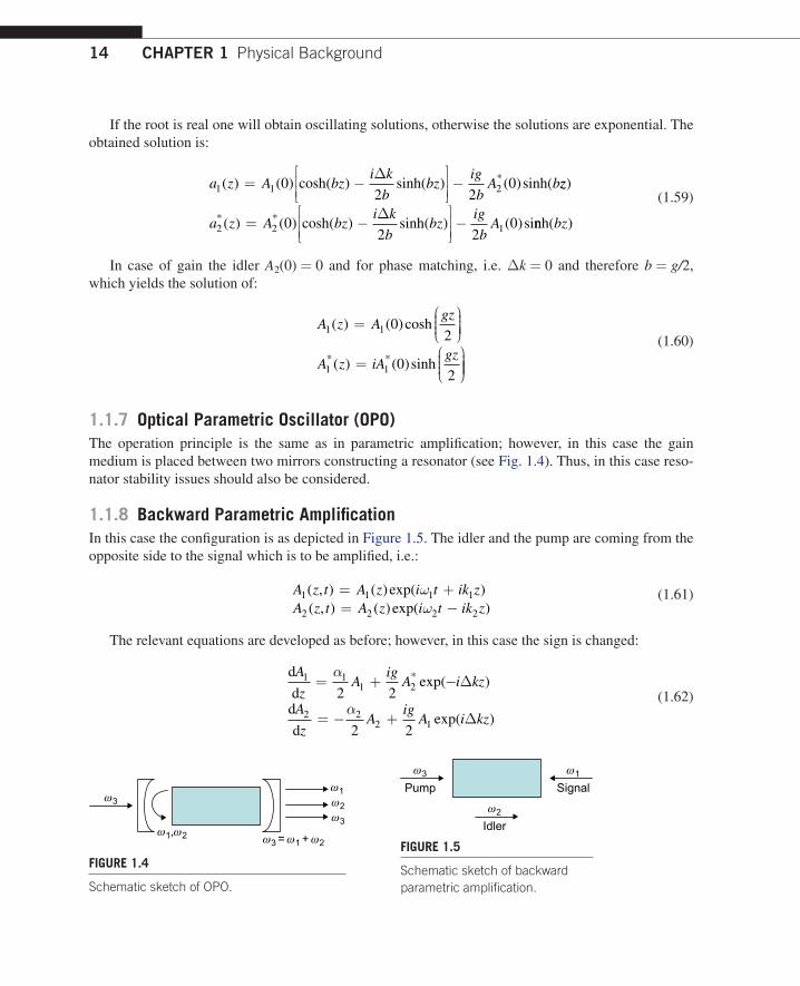
1.1.7 Optical Parametric Oscillator (OPO)The operation principle is the same as in parametric amplification; however, in this case the gain medium is placed between two mirrors constructing a resonator (see Fig. 1.4). Thus, in this case reso-nator stability issues should also be considered.
1.1.8 Backward Parametric AmplificationIn this case the configuration is as depicted in Figure 1.5. The idler and the pump are coming from the opposite side to the signal which is to be amplified, i.e.:
A z t A z i t ik zA z t A z i t ik z
1 1 1 1
2 2 2 2
( , ) ( ) exp( )( , ) ( ) exp( )
= += −
(1.61)
The relevant equations are developed as before; however, in this case the sign is changed:
d
dd
d
A
zA
igA i kz
A
zA
igA i kz
1 11 2
2 22 1
2 2
2 2
= + −
= − +
* exp( )
exp( )
(1.62)
ω3
ω1
ω3
ω2
ω1,ω2 ω3 = ω1 + ω2
FIgURE 1.4
Schematic sketch of OPO.
ω3 ω1
Pump Signal
ω2
Idler
FIgURE 1.5
Schematic sketch of backward parametric amplification.
��
The boundary conditions are A1(L) and A2(0) and the solution is:
A zA L
gLiA
gL
A z
11
2
2
2
02
( )( )
cos( ) tan
( )
*
*
=
−
==
+
A
gLiA L
gL21
0
22
*( )
cos( ) tan
(1.63)
1.1.9 Raman EffectThis effect occurs only in molecules (in atoms it does not exist), in liquids or in solids. The radiation generates dipole oscillations (vibrations) by moving the negative and the positive charges to opposite directions. The generated dipole moment is equal to: ε = 0 E where is the polarizability con-stant. One may develop into Taylor expansion around the spatial point of stability x0:
( ) ( ) ...xx
x xx
= +∂∂
− +0 0
0
(1.64)
while the dipole itself consists of a permanent part and an induced part yielding:
ε ε
= +
= +∂
∂⋅ −
= +∂∂
⋅ −
p i
p pp
i
xx x
Ex
x x
0 0
0 0 0 0
( )
( )) ...⋅ +E
(1.65)
To understand the Raman effect we use the fact that the scattering is proportional to the Fourier transform of the correlation function of the fluctuations in the polarizability function. Vibrations in molecules or phonons in solids modulate the dielectric function or the polarizability and this modula-tion is the origin of the fluctuation. According to Eq. 1.64 the polarizability modulation is given by:
=
∂∂x
x
(1.66)
The correlation function is then given by:
Gx x
xx t t
x
xx trr tt′ ′
′′
′′,
**( )
( )( )
( )=∂ +
∂+
∂∂
(1.67)
�.� Introduction to Non-Linear Optics

�� CHAPTER � Physical Background
where the time dependence appears only in the normal coordinates and therefore it is possible to sep-arate Eq. 1.67 into spatial and temporal parts:
Gx x
x
x
xx t t x trr tt′ ′
′ ′′ ′,
**( ) ( )
( ) ( )=∂ +
∂∂
∂+
(1.68)
The time-dependent part of the correlation function G t x t t x t( ) ( ) ( )*= +⟨ ′ ′ ⟩ is the most important in calculating the scattering cross-section and it gives the frequency dependence. Using the properties of quantum harmonic oscillator it is possible to show that this reduces to the following:
G t n i t n i t( ) ( ) exp( ) ( ( )) exp( )= + + −[ ]
21
(1.69)
where here n( ) is the average number of phonons with frequency which according to Bose–Einstein statistics is given by: n k TB( ) (exp( ) ) = − − / 1 1. The frequency dependence of the Raman scattering cross-section is proportional to the Fourier transform of the time correlation func-tion in Eq. 1.69. The result is:
G n ns s i s i( ) ( ) ( ) ( ( )) ( )
δ δ
= − − + + − +[ ]
21
(1.70)
where here i is the angular frequency of the excitation light and s is the angular frequency of the scattered light. The two parts of this expression represent the anti-Stokes and Stokes branches of Raman scattering. Note that the ratio between the two branches is proportional to ( ( )) ( )1 + n n / which provides a reliable means of measuring temperature from the Raman Stokes to anti-Stokes ratio.
There are different ways to explain the Raman effect, classical, semi-classical and quantum. The non-linearity can be seen if one considers the interaction energy:
ℜ = −′ E
which after the substitution of the previously derived expressions from Eq. 1.66 has the form:
ℜ = −
∂∂
−′ ε
xx x E
x00 0
2( )
This non-linear Hamiltonian is the basis for the Raman effect and leads to the E4 dependence of the scattered intensity. Schematically the effect can be described according to four cases as depicted in Figure 1.6. In this figure a is the annihilation quantum operator which takes the molecules down from a given energetic state. a+ is the quantum generation operator which takes the molecule to higher energetic level:
aa a a+ +− = 1

��
In the figure we assume that in the material there are two types of photons at two radial frequen-cies of s and l. The sub-index v designates the vibration state of the molecule.
The operation principle in spontaneous and stimulated Raman emission is similar to the basic physics of lasers. The gain of the medium is proportional to the population inversion. In spontaneous emission the photons at s are emitted in all directions while the longitudinal concentration of the pumping l photons due to absorption is according to:
N z NDP n
czl l
a l( ) ( ) exp( )
= −
0
where D is a material constant, Pa is the probability of having atoms in energetic level a which is the lower vibration state and n(l) is the refractive index at frequency of l; c is the speed of light.
In the case of stimulated Raman emission, gain is obtained due to the synchronized energetic level transitions (emission). All microscopic dipoles transmit coherently as one unified antenna. As in regu-lar lasing systems the gain is proportional to the population inversion. In this case the longitudinal concentration is:
N z ND P P n n
czl l
a b l l( ) ( ) exp( ) ( )
=−
0
The difference of the probability distribution functions can be obtained by assuming a Maxwell–Boltzmann distribution. Pb is the higher vibration state.
Note that if Nl is larger than a certain constant the number of emitted photons at the difference fre-quency Nv is starting to explode (goes to infinity). It is becoming a self-radiating source that amplifies itself until saturation occurs and our simplified linear modeling is no longer valid. This effect is called Raman parametric instability.
1.1.10 Optical Phase ConjugationThe topic being described here relates to four waves mixing. The idea is to obtain a phase conjugation which can be expressed by generation of an effective “mirror” reflecting the beam back to its origin. In this case all four frequencies are identical and equal to while signals E1 and E2 are pumping sig-nals and E4 is the input signal which is being phase conjugated to signal E3. A schematic sketch of the configuration is seen in Figure 1.7.
Stokes absorption
aval+as
ls
v
Anti-Stokes absorption
av+al
+as
sl
v
Anti-Stokes emission
avalas+
sl
v
Stokes emission
av+alas+
ls
v
FIgURE 1.6
Schematic sketch of the cases related to the Raman effect.
�.� Introduction to Non-Linear Optics

�� CHAPTER � Physical Background
Mathematically the phase conjugation is expressed as:
E E t kz rE E t kz r
4 0
3 0
= − += − −
| || |
cos( ( ))cos( ( )) ϕ ϕ
(1.71)
where ϕ is the spatial phase that is being conjugated.In three waves mixing one obtains:
P E ENL ijk j k≈ ( )2
(1.72)
In four waves mixing one obtains:
P E E ENL mijk i j k≈ ( )3
(1.73)
if denoting:
E r t A r i t ik r
E r t A r i t ik r
1 1 1
2 2 2
1
21
2
( , ) ( ) exp( )
( , ) ( ) exp( )
= −
= −
′
′
EE r t A r i t ikr
E r t A r i t ikr
3 3
4 4
1
21
2
( , ) ( ) exp( )
( , ) ( ) exp( )
= +
= −
′
′
And after assuming phase matching: k1 + k2 = 0 and that | | | | | | | | .A A A A12
22
32
42′ ′ ′ ′, , Substituting E4
into the wave equation yields:
∇ −
∂
∂=
∂
∂2
4
24
2
2
2E
E
t
p
tNLε
where pNL is the non-linear part of the polarization vector. Neglecting d
d
24
2
A
z
′
in comparison to
kA
z
d
d4′
results by the differential coupled wave equation for the fourth wave in the mixture:
d
d| | | |
A
zi A A A i A A A4 3
12
22
43
1 2 32 2
′′ ′ ′ ′ ′ ′= − +
−
ε
ε( ) ( ) **
(1.74)
The solution of this equation is as follows. We denote:
A A i A A z4 43
12
22
2′ ′ ′= − +( )
exp ( ) ε | | | |
(1.75)
E3
E4
E2
E1
FIgURE 1.7
Schematic sketch of optical phase conjugation configuration.

��
to obtain the following coupled equations:
d
dd
d
A
zi A
A
zi A
43
34
*
* *
=
=
κ
κ
(1.76)
where
κ
ε= −
23
1 2( ) A A′ ′ (1.77)
leading to the following equation:
d
d| |
23
22
3A
zi A= κ (1.78)
and the solution is:
A zz
LA L i
z L
L3 3( )cos
cos( )
sin ( )
cos
*
=( )( )
+−( )
( )| |
| |
| |
| | | |
κ
κ
κ κ
κ κAA
A z iz
LA L
z L
4
4 3
0*
*
( )
( )sin
cos( )
cos ( )
c= −
( )( )
+−( )| | | |
| |
| |κ κ
κ κ
κ
oos( )
| |κ LA
( ) 4 0
(1.79)
where L is the size of the non-linear medium.
1.1.11 Quantum Electronics1.1.11.1 IntroductionFor proper construction of our mathematical tools we will denote the position operator as:
q q= (1.80)
where q is the position, while the momentum operator will be denoted as:
p i
q= −
∂∂ (1.81)
The commutation relation is defined as:
ˆ, ˆ ˆ ˆ ˆ ˆp q qp pq i[ ] = − = (1.82)
�.� Introduction to Non-Linear Optics

�0 CHAPTER � Physical Background
The very well-known Schrödinger equation is the basis for our analysis:
it
xm
V x x∂
∂= − ∇ +
( ) ( ) ( )2
2
2 (1.83)
where V(x) is the potential function while a parabolic potential will be assumed. is the wave func-tion. The Hamiltonian operator following the Schrödinger equation is defined as:
H
mV= − ∇ +
22
2 (1.84)
The wave function can be decomposed according to stationary states un as follows:
( , ) ( ) expq t C u qi
E tn n nn
=−
∑
(1.85)
where Cn are the decomposition coefficients and En are the eigenvalues which also have the physical meaning of possible energy levels. Next we intend to show how the energy levels are being quantized.
The stationary states are eigenfunctions:
−∂
∂+
=2 2
22m qV q u q E u qn n n( ) ( ) ( ) (1.86)
which are:
ˆ ( ) ( )Hu q E u qn n n= (1.87)
The energy will be denoted by:
En n= (1.88)
and later on we will express n via the angular frequency of the photons denoted as . Following the definition of the momentum operator, the Hamiltonian operator for the parabolic potential may be expressed as:
ˆ ˆ
ˆHp
mmq= +
2 22
2 2
(1.89)
Two operators will now be defined. The destructor:
ˆ ˆ ˆa m m q ip= ( ) +( )−
21 2 /
(1.90)
��
and the creator:
ˆ ( ) ( ˆ ˆ )/a m m q ip+ −= −2 1 2 (1.91)
From its definition it is clear that:
ˆ, ˆa a+
= 1 (1.92)
Note that the commutator for any operator with a constant (here denoted as c) is always zero:
ˆ, c
= 0 (1.93)
The Hamiltonian may also be defined according to the two new operators as:
ˆ ( ˆ, ˆ) ˆ ˆH p q a a= +
+1
2 (1.94)
Every wave function can be decomposed according to the stationary states as:
( ) ( )q C u qn nn
= ∑ (1.95)
by denoting it as which is called “ket”. It is a column vector of the Cn coefficients that represents a given state or a given wave function. The row vector is denoted as “bra”: . Thus, following those notations the Schrödinger equation can be expressed as:
H H Hn n n= (1.96)
where H n is the vector of coefficients expressing the wave function that solves the equation, accord-ing to the stationary base of functions.
It is easy to show that:
ˆ , ˆ ˆH a a
= − (1.97)
Therefore following Eqs. 1.96 and 1.97 it is simple to obtain that:
ˆ ˆ ˆHa H a Hn n n= −( ) (1.98)
Thus, the distraction operator reduces the eigenvalues which are always non-negative. The reduc-tion can be done until the state becomes a zero state. The definition of the zero state is as follows:
a 0 0= (1.99)
�.� Introduction to Non-Linear Optics

�� CHAPTER � Physical Background
On this state one obtains:
ˆ ˆ ˆH a a01
20
1
20= +
=+ (1.100)
From the last equation one sees that the energy of the zero state is 0 5. and when going to higher energy states each state adds an energy of as seen from Eq. 1.98. Therefore, denoting by n the number of the energetic levels, n is to indicate how many levels there are above the zero state. Thus, in a recursive way one may obtain that:
H n n n
E nn n
= +
= = +
1
21
2
(1.101)
Note that n in our case indicates the energetic level, i.e. it relates to the number of photons in the optical field and it quantizes the energy of the field (which is proportional to the number of photons).
Now defining by Sn the normalization factor which may be found according to:
ˆ ˆ *a n S n n a S nn n= − = −+1 1 (1.102)
Thus,
n a a n S n nnˆ ˆ | |+ = − −2 1 1 (1.103)
since
ˆ ˆ ˆH a a n= +
= +
+ 1
20
1
2 (1.104)
one has:
n a a n n n n n n nˆ ˆ+ = = (1.105)
Since normalization is desired:
n n n n= − − =1 1 1 (1.106)
and therefore Sn = n. Thus,
ˆ ˆa n n n a n n n= − = + ++1 1 1 (1.107)

��
and in a recursive way one obtains that:
n
na n=
10
!( )ˆ (1.108)
Now the states can be allocated. Using a 0 0= this means that:
( ) ( ( )/2 01 20m m q ip q − =ˆ ˆ )ϕ (1.109)
where 0 designates the wave function of the zero state. Thus, substituting the p and q operators as described by Eqs. 1.80 and 1.81 yields:
d
dqq
mq qϕ ϕ0 0( ) ( )= −
(1.110)
The solution for this differential equation is:
ϕ0
1 42
2( ) exp
/
qm m
q=
−
(1.111)
which is already a normalized result. Using Eq. 1.107 yields:
nm
q qn=
Hϕ0 ( ) (1.112)
where Hn is a Hermit polynomial.
1.1.11.2 ObservablesGiven an operator , its observation value is defined as:
= = ∫ˆ ( ) ˆ ( )* q q qd (1.113)
since the wave function can be expressed according to the orthogonal set:
ϕ ϕ( ) ( ) ( ) ( )* * *q a q q a qn nn
n nn
= =∑ ∑ (1.114)
which yields that:
ˆ * * =
a a
l a
a1 1
11 12 13
21
1
2
(1.115)
�.� Introduction to Non-Linear Optics

�� CHAPTER � Physical Background
and according to our representation it becomes:
ˆ ˆ = (1.116)
1.1.11.3 Heisenberg PictureLet us return again to the Schrödinger equation:
i
tH
d
d = ˆ (1.117)
The solution is:
( ) exp ( )t
iHt=
−
ˆ 0
(1.118)
where ( )0 are the initial conditions. After using the stationary states decomposition:
ϕ( ) ( )0 0= ∑cnn
n (1.119)
the stationary states are the eigenvectors, i.e.:
H n n nϕ ϕ= (1.120)
and thus:
ϕ ϕ( ) ( )exp ( )expt ci
H t c i tnn
n nn
n n=−
= −( )∑ ∑0 0
ˆt (1.121)
The observation variable is:
ˆ ( ) ˆ ( ) ( ) exp ˆ ˆ exp ˆ t
t ti
Hti
Ht= =
−
0
= ( ) ( ) ˆ( ) ( )0 0 0t (1.122)
Note that if one uses the Schrödinger picture the time variation is inside the wave function (t) while the operator is a stationary one. In the Heisenberg picture the wave functions are stationary (0) and the time variation is inserted into the operator ˆ( ) t .
Thus, the time-varying operator is equal to:
ˆ( ) exp ˆ ˆ exp ˆ ti
Hti
Ht=
−
(1.123)
��
Derivation of the last equation yields:
d
dtt
iH t t H
iH tˆ( ) ˆ ( ) ( ) ˆ ˆ , ˆ( ) = −( ) =
(1.124)
The last equation is called the Heisenberg motion equation.
1.1.11.4 Quantum Description of MoleculesSo far we have discussed the quantization of the photonic field and now we add another dimension to the problem related to the energetic levels of the atom/molecule. In our analysis we shall assume a two-level system (TLS). In this case the wave function of the system will be described by the state’s decomposition while for each level there may be a different state decomposition and a different number of photons n. We shall denote the two states by a and b:
ab a bc a c b= + (1.125)
which means that the atomic states can be represented using vectorial notation as:
→
→
→
c
ca ba
b
, ,1
0
0
1 (1.126)
The coefficients will be normalized:
| | | |c ca b2 2 1+ = (1.127)
The operators will be represented as:
11 12
21 22
(1.128)
while all operators are hermitic operators:
12 21= * (1.129)
The Hamiltonian will be:
Haba
b
=
0
0 (1.130)
which means that:
ˆ ˆH a a H b bab a ab b= = (1.131)
�.� Introduction to Non-Linear Optics
�� CHAPTER � Physical Background
We will define two other operators having similar meaning as the creation and the annihilation (or destruction) operators but here the operation is between the two levels of the atom and not within the energy of the field as before:
ˆ ˆ + −=
=
0 1
0 0
0 0
1 0 (1.132)
They have similar meaning to the operators ˆ , ˆa a+ operating on the field because here as well one has:
ˆ ˆ ˆ ˆ + + − −= =
= =
b a a a b b
0
0
0
0 (1.133)
1.1.11.5 Interaction Between Atoms and RadiationA given state will be described as n m where n is the number of photons and it describes the field quantization (n = 0,1, 2,) and m is the atomic level which in TLS is m = 1, 2.
In the case where there is no interaction between the radiation and the atom one can write the fol-lowing Hamiltonian:
ˆ ˆ ˆ ˆ ˆH H H a aatom fielda
b
= + =
+ +
+
0
01
2 (1.134)
We denote the dipole operator as:
ˆ ˆp eq= − (1.135)
where e is the charge of an electron. Assume that:
ˆ ˆ ˆ ,*
*pp p
p p
p
pp paa ab
ba bb
=
=
= ++ −0
0 (1.136)
due to the symmetry of the wave function a aq q( ) ( )= ± − which makes paa = pbb = 0.The potential energy is defined as:
ˆ ˆ ˆv pE= (1.137)
The electrical field of a harmonic oscillator can be obtained by solving the Maxwell equations with the boundary conditions of zero field at two mirrors positioned distance L apart (standing wave):
E q zt q tmV
kzx( , , ) ( ) sin= ( )2 2
0
ε
(1.138)

��
where V is the volume and:
k
cmL
= =
(1.139)
with c being the speed of light and m is an integer number. In an operator representation one obtains:
ˆ ˆ ˆ sin( )EV
a a kz= +( )+ε0
(1.140)
Thus the potential energy operator will be:
ˆ sin( ) ˆ ˆ ˆ ˆv pV
kz a a= +( ) +( )+ + −ε
0
(1.141)
leading to the following Hamiltonian:
ˆ ˆ ˆ ˆ ˆ ˆH a a g a aa
b
=
+ +
+ +( )+ + +
0
01
2 ++( )− (1.142)
with
gp
Vkz=
ε0
sin( ) (1.143)
One may neglect the combination of ˆ ˆa− and ˆ ˆa+ + since this means that either the atom goes to lower energy level and radiation is absorbed rather than generated (first term) or the atom goes to higher energetic level and radiation is generated. The probability for both is very low. Thus, one remains only with:
ˆ ˆ ˆ ˆ ˆ ˆ ˆH a a g a aa
b
=
+ +
+ ++ + −
0
01
2 ++( ) (1.144)
The solution for the wave function will be:
( ) ( ),,
t c t n mn mn m
= ∑ (1.145)
Substituting this into the Schrödinger equation of Eq. 1.83 we obtain:
it
c t n m c t H n mn mn m
n mn m
d
d 1 1 11 1
1 1 11 1
1 1,,
,,
( ) ( )∑ ∑= ˆ (1.146)
�.� Introduction to Non-Linear Optics
�� CHAPTER � Physical Background
Multiplying by bra of n m2 2 , and due to orthogonality:
n m n m n n m m2 2 1 1 1 2 1 2= δ δ, , (1.147)
results with:
d
dtc t n m H n m c tn m n m
n m2 2 2 2 1 1 1 1
1 1, ,
,
( ) ( )= ∑ ˆ (1.148)
Computing the coefficients n m H n m2 2 1 1ˆ appearing in Eq. 1.148 yields:
n m H n m
n m H n m n
atom m n n m m
field
2 2 1 1 1 2 1 2
2 2 1 1 1
1
1
2
ˆ
ˆ
, ,=
= +
δ δ
= ++ − +
δ δ
n n m m
n m v n m g n m a a n m
1 2 1 2
2 2 1 1 2 2 1 1
, ,
ˆ ˆ ˆ ˆ ˆ
(1.149)
where:
g n m a a n b g n m n n b n g n n m b2 2 1 2 2 1 1 1 1 1 2 21 1 1ˆ ˆ ˆ ˆ , ,+ − +
++ = + + = + δ δ
gg n m a a n a g n m n n b n g n n m a2 2 1 2 2 1 1 1 1 1 2 21ˆ ˆ ˆ ˆ , ,+ − +
−+ = − = δ δ
(1.150)
therefore one may obtain for TLS:
it
c t c n c nn a n a a n b d
d , , ,( ) = +
+
+ +
1
2 1 ++
= +
+
+ +
1
3
21 1
g
it
c t c nn b n b bd
d , ,( ) + +c n gn a, 1
(1.151)
Denoting:
c c i n tn a n a a, , exp= − +
+
1
2
= − +
+
+ +c c i n tn b n b b1 1
3
2, , exp
(1.152)
the new equations become:
d
dd
d
tc t ic n g i t
tc t
n a n b a b
n b
, ,
,
( ) exp
( )
= − + − − −( )( )( )=
+
+
1
1
1
−− + − −( )( )( )ic n g i tn a a b , exp1
(1.153)
��
We assume the resonance condition:
≈ −( ) a b (1.154)
By two derivations of the coupled equations one obtains:
d
d
2
22 1
c
tg n cn a
n a,
,( )= − + (1.155)
which yields:
c A g n t B g n t
c iA g n t iB g n t
n a
n b
,
,
sin cos
cos sin
= +( ) + +( )= +( ) − ++
1 1
1 11 (( ) (1.156)
If choosing the initial conditions of:
c cn a n b, ,( ) ( )0 0 0 11= =+
one obtains A i B= − =, 0 and thus the solution becomes:
c i g n t c g n tn a n b, ,sin cos= − +( ) = +( )+1 11 (1.157)
One may see that there are oscillations at frequency of g n + 1 which is called the Rabi frequency:
εRabi
g n p
Vn kz=
+= +
1
2 21
0
sin( ) (1.158)
Since the observation value for E2 is equal to:
E n E n
Vn kz ER M S
2 2
0
2 221
2= = +
=
ε
sin ( ) . . (1.159)
therefore the Rabi frequency is actually proportional to the R.M.S. (root mean square) value of the field:
Rabi R M Sp
E≈4 . . . (1.160)
�.� Introduction to Non-Linear Optics

�0 CHAPTER � Physical Background
1.2 BASICS OF SEMICONDUCTORSIn this subsection we intend to derive the basic equations describing the physical effects in semi-conductors [3]. Those effects are relevant to electrical as well as photonic devices built from semiconductors.
1.2.1 Intrinsic SemiconductorStarting from the Kronig and Penney model which assumes periodic potential, the linear Schrödinger equation is:
− ∂
∂+ =
∂∂
2 2
22m
x t
xV x x t i
x t
t
( , )( ) ( , )
( , ) (1.161)
where is the wave function, V is the potential, m is the mass, (x,t) are the spatial and time coordinates respectively and = h/2 while h is the Planck constant. Since a periodic potential is assumed thus:
V x V x nl n( ) ( ) , , ...= + = 1 2 3 (1.162)
l is the basic cell of the crystal. Figure 1.8 presents the potential function along the crystal.Assuming that N is the number of atoms in the crystal and that there are periodic boundary conditions:
( ) ( )x Nl x+ = (1.163)
The solution according to Floquet’s theorem is the Bloch wave function:
( ) ( ) exp( )x u x x= (1.164)
is a constant and u(x) is periodic with l:
u x u x l( ) ( )= + (1.165)
In the case that V0 = 0 one needs to obtain the free electron solution and thus in that case one needs to have:
u x ik( ) = =0 (1.166)
where k is the crystal’s wave vector.Due to the periodicity constraint one has:
u x Nl x Nl u x x( ) exp[ ( )] ( ) exp( )+ + = (1.167)
which yields
exp( )
Nl
n
Nli ki= → =
=1
2 (1.168)
V(x)
V0
E
b0
x
2ll
FIgURE 1.8
Model of periodic potential in the crystal.

��
The Schrödinger equation will now be solved by the parameter separation method. Defining:
( , ) ( ) ( )x t x t= Φ (1.169)
after substitution we have:
−+
= =
2 2
22m
x
xx V x
x
t
ti
tE
d
dd
d
( )( ) ( )
( )
( )
( )
Φ
Φ
(1.170)
where E is the constant eigenvalue having the physical meaning of energy. The last equation leads to the following equations set:
d
dd
d
2
2 12
2
2 22
0
0 0 0
0
xk V x x b
xk V x V b x l
+ = = ≤ ≤
− = = ≤ ≤
( ) ,
( ) ,
(1.171)
While defining as follows: in the spatial region where V(x) = 0:
E
P
m
k
m= =1
2 212
2 2
(1.172)
and in the region where V(x) = V0:
V E
P
m
k
m022 2
22
2 2− = =
(1.173)
Those definitions follow the relation between momentum P and energy E. The solution of the dif-ferential equations of Eq. 1.171 is:
( ) exp( ) exp( )( ) exp( ) exp( )x A ik x B ik x x bx C k x D k x b
= + − ≤ ≤= − +
1 1
2 2
0≤≤ ≤x l
(1.174)
Since the wave function is periodic with the structure:
( ) ( ) exp[ ( )] ( ) exp( )exp( ) ( ) exp(x l u x l ik x l u x ikx ikl x ikl+ = + + = = )) (1.175)
one obtains that for l < x < l + b:
( ) [ exp( ( )) exp( ( ))]exp( )x A ik x l B ik x l ikl= − + − −1 1 (1.176)
�.� Basics of Semiconductors

�� CHAPTER � Physical Background
The requirement on the continuity of the wave function and its derivative at x = b and x = l and thus at x = b gives:
A ik b B ik b C k b D k bik A ik b
exp( ) exp( ) exp( ) exp( )[ exp( )
1 1 2 2
1 1
+ − = − +− BB ik b k C k b D k bexp( )] [ exp( ) exp( )]− = − − +1 2 2 2
(1.177)
and at x = l:
C k l D k l A B iklk C k l D k l
exp( ) exp( ) ( ) exp( )[ exp( ) exp( )
− + = +− − +
2 2
2 2 2 ]] ( ) exp( )= −ik A B ikl1
(1.178)
The solution of those two equations leads to the following relations:
[cos( )][cosh( )] [sin( )][k b k lk k
k kk b1 2
12
22
1 212
−−
ssinh( )] cos( )
[cos( )][cosh( )]
k l kl E V
k b k lk k
k k
2 0
1 212
22
1 22
= <
−+
= >[sin( )][sinh( )] cos( )k b k l kl E V1 2 0
(1.179)
Since N is a very large number, k can practically be considered as a continuous variable. The right wing is bounded by the values range of [−1,1] while the left wing can obtain larger and smaller values. Therefore only values of E/V0 for which cos(kl) is real can solve the equation and this is the reasoning for the appear-ance of the forbidden energy bands. Thus, the allowed energy bands are bounded by the positions for which cos(kl) equals +1 and −1. Because the right wing is a cosine function which is periodic at 2/l, each energetic band corresponding to k varying within the range of 2/l is called a Brullouin zone.
In semiconductors the last allowed energetic band for which the electrons are still connected to the atom is called the valence band. The band above it is called the conduction band where the electrons are already free from the crystal. The forbidden energetic band separating the two is denoted as Eg. In semiconductors the thermal energy which is proportional to kBT (where kB is Boltzmann constant and T is the temperature) is smaller in comparison to Eg but not significantly smaller as in an insulator.
We will now derive the equation describing the concentration of free electrons and holes. Note that every free electron going from the valence band to the conductance band leaves a positively charged defect in the crystal. This defect is called a hole which is actually a lack of bounded electron. The holes can move in the crystal and generate a current similarly to what happens with free electrons.
The concentration of free carriers is equal to:
Concentration of freecarriers in the energy band
=
Concentration of allowedstates in the energy band
×
Probablity of occupyingthose states
The Fermi–Dirac distribution is the probability of occupying the electronic states:
f EE E
k T
FDF
B
( )
exp
=
+−
1
1 (1.181)
(1.180)
��
where EF is the Fermi energy which is a constant in the distribution expression and T is the tempera-ture. Denoting by dn(E) the concentration of free electrons in the energy band and by Nc(E) the con-centration of allowed states, thus:
d dn E N E f E Ec FD( ) ( ) ( )= (1.182)
Assuming that nx designates the number of atoms per every face of the crystal, then:
n
L
l
Length of face
Dis ce between atomsxx
x
= =
tan (1.183)
The same is true for the other two faces. The size of the Brullouin zone along the x axis face is 2/lx and thus every allowed state occupies along the kx direction, a region having dimensions of kx where:
k
Overall length of zone
Total number of its states
lx
x= =
/2LL l Lx x x/
=2 (1.184)
The volume occupied by each state in the k space is therefore:
Volume of a state k k kL L Lx y z
x y z
= =1
2
2
2
3
( )
(1.185)
The factor of 2 is appearing in the equation because one volume is occupied by two states each having electrons with opposite spins. Defining by dN9 the number of allowed states within an infini-tesimally thin shell (width of dk) with radius k, in the k space:
d
dN
Total volume of shell
Volume of a gle state
k k′ = =
sin
4
2
2
( )3
2
2L L L
L L Lk
k
x y z
x y z=
d (1.186)
The lower part of the conductance band may be approximated by a parabolic approximation:
E Ek
mc
e
= +2 2
2 * (1.187)
where Ec is the lowest energy of the conductance band and me* is a constant which is the effective
mass of the free electron. Therefore one obtains:
k
mE Ee
c= −2 *
(1.188)
�.� Basics of Semiconductors

�� CHAPTER � Physical Background
and thus
dd
km E
E E
e
c
=−
2
2
*
(1.189)
yielding:
dd d
/N
L L L hm E E E N E E
x y ze c c
′=
( ) − ≡
42
3
3 2 * ( ) (1.190)
where Nc(E) is the concentration of the allowed states for the electrons in the energetic band of [E, E + dE] per volume of the crystal:
N E
hm E Ec e c( ) *=
( ) −
42
3
3 2 / (1.191)
This is also called the density of states. Similar derivation can be performed for the holes in the valence band and one may obtain:
N E
hm E Ev h v( ) *=
( ) −
42
3
3 2 / (1.192)
where mh* is the effective mass of the holes and Ev is the upper energetic level of the valance band.
Following Eq. 1.180 the number of electrons in the conductance band is equal to:
d d/
n E N E f E Eh
m E Ec FD e c( ) ( ) ( ) *= × =
( ) −
42
13
3 2
11 +−
expE E
k T
EF
B
d (1.193)
The total number of electrons is obtained by integrating over the range of energies relevant to the conductance band:
n n E n Eh
mE E
i
E
E E
E
ec
c
c
c
= ≈ =
( ) −
+
+ ∞
∫ ∫d d/
( ) ( )
e
*
42
13
3 2
xxp
e
*
E E
k T
E
hm
E E
F
B
E
ec
c
−
≈
( ) −
∞
∫ d
/42
3
3 2
xxpE E
k T
EF
B
Ec
−
∞
∫ d
(1.194)

��
The obtained result is as follows:
nh
m k TE E
k TN
E E
k Ti e BF c
Bc
F c
B
= ( ) −
≡−
22
3
3 2* exp exp/
(1.195)
Similar derivation may be performed for the holes; however, in their case the distribution should be 1 − fFD because the probability of occupying the valence states by holes is equal to the probability of not occupying them by electrons. Therefore the expression for the hole concentration will be:
ph
m k TE E
k TN
E E
k Ti h Bv F
Bv
v F
B
= ( ) −
≡−
22
3
3 2* exp exp/
(1.196)
In intrinsic semiconductors one has electrical neutrality and thus ni = pi which leads to:
n n p N NE E
k Ti i i c vv c
B
2 = =−
exp (1.197)
since
E E Eg c v= − (1.198)
One obtains:
n N NE
k Ti c vg
B
=−
exp2
(1.199)
From ni = pi one may also obtain that:
EE E k T N
NFc v B v
c
=+
+
2 2
ln (1.200)
1.2.2 Extrinsic SemiconductorWhen doping is added the semiconductor is no longer called intrinsic but rather extrinsic. The electri-cal neutrality can then be written as:
n N p Na d+ = + (1.201)
where Na and Nd are the concentrations of the acceptors (atoms that accept one electron from the crystal) and donors (atoms that donate one electron to the crystal) respectively. n and p are the con-centrations of free electrons and holes respectively. In thermal equilibrium one obtains:
np ni= 2 (1.202)
�.� Basics of Semiconductors

�� CHAPTER � Physical Background
In p-type material one has Na >> pi,Nd and in n-type material the doping is such that Nd >> ni,Na and thus in n-type material one has:
n N p
n
Ndi
d
≈ =2
(1.203)
and in p-type:
p N n
n
Nai
a
= =2
(1.204)
Using Eq. 1.195 one has in n-type:
E E k TN
NF c Bc
d
= −
ln (1.205)
and in p-type, following Eq. 1.196:
E E k TN
NF v Bv
a
= +
ln (1.206)
1.2.3 CurrentsAccording to Fick’s law the flux is proportional to the gradient of the concentration:
F D
n
x= −
d
d (1.207)
where D is the diffusion constant, F is the flux and n is the concentration. The current in the semi-conductor can be divided into two types: current due to diffusion and current due to drift. Drift is movement of free carriers due to electrical field. The drift current equals:
I qA nE qA pEdrift n p= + (1.208)
where q is the charge of an electron (1.6 10−19[cb]), A is the cross-section area, n and p are the mobility of electrons and holes respectively. n and p are the free concentrations of electrons and holes and E is the applied electrical field.
The current due to diffusion is equal to:
I qAD
n
xqAD
p
xdiffusion = −d
d
d
d (1.209)

��
Following the Einstein equation there is a relation between mobility and diffusion constant D:
D D k T
qp
p
n
n
B
= = (1.210)
1.2.4 Recombination and generationOnly the case of weak injection will be discussed, which is the case where the free carriers, which are gen-erated due to the absorption of the external illumination, are large in comparison to the minority carriers but negligible in comparison to the majority carriers. Thus, in this case it is interesting to observe the change only to the minority carriers (electrons in p-type and holes in n-type semiconductors). The rate equation in the case of external illumination generating GL free carriers per unit volume per unit time is equal to:
d
d
p
tG R G
p pnL p L
n on
p
= − = −−
(1.211)
where Rp is the recombination of holes (in units of concentration per unit of time), pon is the holes concentration in the n-type material in the steady state (without illumination) and p is the recom-bination time constant. For p-type material the equation is identical but instead of pn one has np and instead of p will be n.
Given illumination power of P illuminating volume of V with photons at frequency of (each photon has energy of h) where the quantum efficiency of conversion of photon into an electron is equal to Q.E, one has:
G
P Q E
VhL =
(1.212)
1.2.5 Continuity EquationThis equation is related to the mass conservation law. It says that the rate of variation of carriers per unit volume Adx (A is the cross-section) is equal to the rate of the carriers going into that volume minus those which are going out of the volume and plus those which are being generated in that volume:
∂∂
=−
−+
−
+ −
∂∂
=
n
tA x
I x
q
I x dx
qG R A x
p
tA x
I x
n nn n
p
d d
d
( ) ( )( )
( )
I x dx
qG R A x
pp p−
+
+ −( )
( ) d
(1.213)
where Gn and Gp are the generation of electrons and holes, respectively. Since
I x x I x
I x
xx( ) ( )
( )+ ≈ +
∂∂
d d (1.214)
�.� Basics of Semiconductors

�� CHAPTER � Physical Background
one obtains:
∂∂
=∂
∂+ −
∂∂
=−
∂
∂+ −
n
t qA
I x
xG R
p
t qA
I x
xG R
nn n
pp p
1
1
( )
( ) (1.215)
Since according to Eqs. 1.208 and 1.209 one has:
I qA n E Dn
x
I qA p E Dp
x
n n n
p p p
= +∂∂
= −∂∂
(1.216)
this yields the following final expression:
∂
∂=
∂∂
+∂
∂+
∂
∂+ −
−
∂∂
= −∂
n
tn
E
xE
n
xD
n
xG
n n
p
tp
E
pp n n
pn
pn
p p
n
nn p
2
2
0
∂∂−
∂∂
+∂
∂+ −
−x
Ep
xD
p
xG
p pp
np
np
n n
p
2
20
(1.217)
1.2.6 p–n JunctionWhen p- and n-type semiconductors are connected, a junction is generated. The junction is a depletion region where only the doping ions remain and there are no free carriers. The free carriers are elimi-nated due to recombination of holes which are majority free carriers in the p-type semiconductor with electrons which are the majority free carriers in the n-type semiconductor. Due to the recombination an electrically charged region is generated on both sides of the junction (depletion region) because the non-mobile ions remain exposed (positive ions in the n-type and negative in the p-type side) while the free carriers disappear. This region is growing while recombination occurs. However, in the generated charged depletion region an electrical field is created which resists the arrival of additional free carri-ers coming to recombine. Eventually the process reaches a steady state fixing given size for the deple-tion region. In order to develop the related physical relations we will use the Poisson equation:
d
d
E
x s
=ε
(1.218)
where is the overall volume charge, E is the electrical field and εs is the relative dielectric coefficient of the semiconductor (the square of the refractive index). In the semiconductors case:
= − − +q N n N pd a( ) (1.219)

��
We denote the size of the junction in the p-type side as xp and in the n-type as xn (see schematic sketch in Fig. 1.9).
In our case assuming:
d
d
E
x
qNx x
qNx x
d
sn
a
sp
=
< <
−− < <
ε
ε
0
0
(1.220)
then
E
qNx x x x
qNx x x x
d
sn n
a
sp p
=
−− < <
−+ − < <
ε
ε
( )
( )
0
0
(1.221)
The electric field is continuous and it also equals zero outside the junction region, thus:
E E
E x E xn p
n p
( ) ( )
( ) ( )
0 0
0
+ −== − =
(1.222)
which yields
E E
qN x qN xa p
s
d n
smax ( )= = =0
ε ε (1.223)
p-type n-type
x
Charge
–xp
xn
–Na
Nd
FIgURE 1.9
Schematic sketch of the charge in the depletion region.
�.� Basics of Semiconductors

�0 CHAPTER � Physical Background
which leads to the electrical neutrality relation of:
N x N xa p d n= (1.224)
Following Eqs. 1.195 and 1.196 one has:
n NE E
k Tp N
E E
k Ti cFi c
Bi v
v Fi
B
=−
=−
exp exp
nn N NE E
k Tp N N
E E
k Td cF c
Ba v
v F
B
= =−
= =−
exp exp
Thus the potential on both sides is equal to:
Vq
E E k TN
n
Vq
E E
n Fi Fx x
Bd
i
p Fi Fx x
n
≡ − − =
≡ − −
>
<−
1
1
( ) ln
( )pp
k TN
nBa
i
=
ln
(1.225)
where EFi is the intrinsic Fermi level and EF is the actual Fermi level. q is the charge of an electron. Thus, the inherent built-in potential is equal to:
Vk T
q
N N
nbi
B a d
i
=
ln
2 (1.226)
and the solution for the potential inside the junction is equal to:
V xqN
x x V
V xqN
x x V
pa
sp p
nd
sn n
( ) ( )
( ) ( )
= + +
=−
− −
2
2
20
20
ε
ε
(1.227)
while the difference between the two constants Vp0 and Vn0 is the built-in potential Vbi. Because the potential is continuous, Vp(0) = Vn(0) and one obtains:
V V V
qNx
qNxbi n p
a
sp
d
sn= − − = +0 0
2 2
2 2ε ε (1.228)
Using the last equations yields:
xN V
qN N Nx
N V
qN N Nns a bi
d a dp
s d bi
a a d
=+
=+
2 2ε ε( ) ( )
(1.229)

��
and the overall size of the depletion region W equals:
W x xq
N N
N NVn p
s a d
a dbi= + =
+
2ε
(1.230)
Figure 1.10 schematically presents the field, potential and energy band bending in the p–n junction region.
In the case where voltage is applied the last equation will become:
W x xq
N N
N NV Vn p
s a d
a dbi= + =
+
−2ε
( )
(1.231)
If one applies backward voltage, V is negative and for forward voltage connection, V is positive. Thus, backward voltage increases the depletion area. The dependence of the depletion region on the voltage creates capacitance C because there is a space charge Q. For a p+n junction (the p-type side is much more heavily doped than the n-type side) one has:
Q qAN x A q V V Nd n s bi d= = −2 ε ( )
(1.232)
The size of the depletion region will be:
WqN
V Vs
dbi= −
2ε( )
(1.233)
and thus the capacitance is:
CQ
VA
q N
V VA
Ws d
bi
s= =−
=d
d
ε ε2( )
(1.234)
1.2.7 Carriers InjectionAs one may see before in thermal equilibrium one has the following relations:
n p n
n p nn n i
p p i
0 02
0 02
==
(1.235)
Since in equilibrium
p N n Np a n d0 0≈ ≈
(1.236)
p-type n-type
x–xp
xn
Emax
Field
p-type n-type
–xp xnx
Vbi
Potential
p-type n-type
Energy bands
ECEF
EFi
Ev
FIgURE 1.10
Schematic presentation of the field, potential and energy band bending in the p–n junction region.
�.� Basics of Semiconductors
�� CHAPTER � Physical Background
using Eq. 1.228 one has:
Vk T
q
n
n
k T
q
p
pbiB n
p
B p
n
=
=
ln ln0
0
0
0
(1.237)
and from here it is simple to obtain that:
n nqV
k T
p pqV
k T
n pbi
B
p nbi
B
0 0
0 0
=
=
exp
exp
(1.238)
Based on those relations one may extract the equations also not in equilibrium:
n nq V V
k T
p pq V V
k T
n pbi
B
p nbi
B
=−
=−
exp( )
exp( )
(1.239)
By substituting the equations one into the other yields:
n nqV
k T
p pqV
k T
p pB
n nB
=
=
0
0
exp
exp
(1.240)
Using the continuity equation for the n side of the diode gives the following steady-state relation:
Dp p
x
p pp
n n n n
p
∂ −
∂−
−=
20
20 0
( )
(1.241)
To have the last equation it was assumed that the electrical field is zero (which is correct outside the junction) and a steady-state condition ∂/∂t = 0. The solution of this differential equation is:
p x p pqV
k T
x
Dn n n
B p p
( ) exp exp= +
−
−
0 0 1
(1.242)

��
where the following boundary conditions were used:
p xp p
qV
k Tx
p xn
n nB
n
( )( ) exp
==
=
= ∞
0 00
0
(1.243)
where the diffusion length is defined as:
L Dp p p≡
(1.244)
The diffusion current is thus:
I x qAD
p
xqAD
p
L
qV
k Tp pn
pn
p B
( ) exp= − =
−
d
d0 1
−
exp
x
Lp
(1.245)
Similar derivation after being performed for the n side of the diode yields:
I x qAD
n
L
qV
k T
x
Ln np
n B n
( ) exp exp=
−
−
0 1
(1.246)
Near the junction the current is mainly a diffusion current of the minority carriers. Away from the junction the current is mainly a drift current of majority carriers. The summation between In and Ip is the total current and it must be constant along the device (a basic rule in electricity). Thus, to find the overall current one needs to sum the electron’s diffusion current in the p-type side of the junction and the hole’s diffusion current in the n-type side and obtain:
I I I qA D
n
LD
p
L
qV
k Tp n np
np
n
p B
= + = +
( ) ( ) exp0 0 0 0
−
1
(1.247)
Figure 1.11 presents how In and Ip look like along the diode.The conceptual understanding of Figure 1.11 is actually rather simple. Starting from the left side
there is a majority of holes. They move to the right. While doing so they are absorbed (recombination) and their concentration is exponentially reduced. The absorption of the holes generates a current of electrons which is exponentially increasing. The summation of both currents is constant. In the deple-tion region of the junction there is no absorption (generation/recombination) and thus both electrons as well as holes preserve their concentration or current level.
Following Eq. 1.242 one may see that the forward voltage generates significant increase in the minority carriers near the junction. This is what is responsible for the strong diffusion current of minority carriers in that region. This also generates a capacitance. The charge there is:
Q qApx x
L
qV
k Tnn
p B
= −−
−
0 1exp exp
=
−
∞
∫ dx
qAp LqV
k T
x
n pB
n
0 1exp
(1.248)
�.� Basics of Semiconductors

�� CHAPTER � Physical Background
and thus the diffusion capacitance is:
CQ
V
q Ap L
k T
qV
k Tdifon p
B B
= =
d
d
2
exp
(1.249)
1.2.8 MOS CapacitorsThe Fermi level of the energy EF remains fixed in steady state. In the metal-oxide-semiconductor (MOS) device, because of the oxide separating the metal and the semi-conductor, no current is generated. Therefore the Fermi
level remains non-bended while the rest of the energetic levels bend according to the externally applied voltage. This may create an effect in which near the oxide the position of EF will become close to Ev or to Ec while assuming a p-type device creates accumulation of free carriers or inversion (the majority of free carriers near the oxide become electrons and not holes). This can easily be seen from the energy band diagram of Figure 1.12.
We denote by (x) the energy bands bending at the semiconduc-tor at position x from the interface with the oxide. In our notations (x = 0) = s and EFi designates the position of the intrinsic Fermi level which according to Eq. 1.200 is approximately:
E
E EFi
c v≈+2
(1.250)
The equation for the MOS device will now be derived. According to the Poisson equation:
d
d
2
2
εx
x
s
= −( )
(1.251)
while
E x
x( ) = −
d
d
(1.252)
Assuming a p-type semiconductor yields:
( ) [ ( ) ( ) ] [ ( ) ( ) ]x q p x n x N q p x n x p np p a p p p p= − − = − − +0 0
(1.253)
p-type n-typeDepletionregion
Ip InItotal
–xp xnx
FIgURE 1.11
Current of holes and electrons as it is distributed along the diode.
Oxide (o) Semiconductor (s)
xx = 0
Ec
EFi
Ev
EFψF
ψs
ψ(x)
FIgURE 1.12
Energy band in MOS capacitor.

��
From Eqs. 1.238 and 1.239 one also knows that:
p x pq x
k T
n x nq x
k T
p pB
p pB
( ) exp( )
( ) exp( )
= −
=
0
0
(1.254)
Therefore the obtained differential equation is:
d
d
2
2 0 01
ε
x
qp
q
k Tn
sp
Bp= − −
−
−exp exppq
k TB
−
1
(1.255)
with the boundary conditions of:
( )xx
xs
=→ ∞=
0
0
(1.256)
The solution for the electrical field is:
E x
xsign
k T
qLF xs
B
DF( ) ( ) ( ( ), )= − =
d
d
2
(1.257)
where
ε
F Fi F
DB s
i
E E
Lk T
n q
= −
=2 2
(1.258)
and
F xq
k T
q
k T
q
kFF
B B B
( ( ), ) exp exp
=
−
+TT
q
k T
q
k TF
B B
−
+ −
−1 exp exp qq
k TB
−
1
(1.259)
The constant LD is called Debye length.According to the Gauss law, from the field one may find the total charge per unit area Qs:
Q E x sign
k T
qLF xs s s
s B
DF= − = = −ε
ε ( ) ( ) ( ( ), )0
2
(1.260)
�.� Basics of Semiconductors
�� CHAPTER � Physical Background
We assume a flat band case, i.e. without applying voltage the energy bands are flat. In this case the operation ranges are as follows: for s < 0 one has accumulation of holes. For = 0 the energy bands are flat. For 0 < s < F one talks about depletion and for s > F one has inversion, while for F < s < 2F one has weak inversion and for s > 2F it is considered to be a strong inversion which is defined as inversion for which the energy band bending generates concentration of electrons which is equal to or larger than Na.
If using Eq. 1.260 and substituting there s = F (passing from depletion to weak inversion) one obtains:
Qk T
qL
q
k T
q
k Ts sB
D
F
B
F
B
= −
ε 2
2exp
(1.261)
Since it is known from Eq. 1.225 that
FB a
i
k T
q
N
n=
ln
(1.262)
one obtains:
Q qNs s a s= − 2ε
(1.263)
which is exactly the equation one may obtain from the depletion region relations of Eqs. 1.229 and 1.230:
Q qN x qNqNs a p a
s s
a
= − = −2ε
(1.264)
The total capacitance of the MOS will be:
1 1 1 2
C C C q N
t
tot s ox
s
s a
ox
ox
= + = +ε ε
(1.265)
where εox is the dielectric constant of the oxide (square of the refraction index in the oxide) and tox is the width of the oxide layer. The expression of Cox is related to the inversion layer or the accumula-tion layer generated on the interface between the oxide and the semiconductor. Cs is the capacitance created due to the depletion region generated in the semiconductor. In the accumulation state or in the inversion state the capacitance is equal only to Cox.
Let us now compute the external voltage one needs to connect to the gate of the MOS in order to shift it into a strong inversion state. The gate voltage VG is equal to the voltage falling on the oxide plus the one on the semiconductor:
V VG ox s= + (1.266)
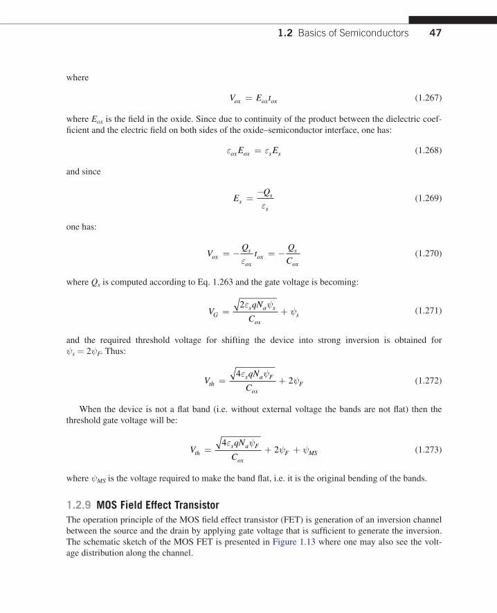
��
where
V E tox ox ox= (1.267)
where Eox is the field in the oxide. Since due to continuity of the product between the dielectric coef-ficient and the electric field on both sides of the oxide–semiconductor interface, one has:
ε εox ox s sE E= (1.268)
and since
E
Qs
s
s
=−ε
(1.269)
one has:
V
Qt
Q
Coxs
oxox
s
ox
= − = −ε
(1.270)
where Qs is computed according to Eq. 1.263 and the gate voltage is becoming:
V
qN
CGs a s
oxs= +
2ε
(1.271)
and the required threshold voltage for shifting the device into strong inversion is obtained for s = 2F. Thus:
V
qN
Cths a F
oxF= +
42
ε
(1.272)
When the device is not a flat band (i.e. without external voltage the bands are not flat) then the threshold gate voltage will be:
V
qN
Cths a F
oxF MS= + +
42
ε
(1.273)
where MS is the voltage required to make the band flat, i.e. it is the original bending of the bands.
1.2.9 MOS Field Effect TransistorThe operation principle of the MOS field effect transistor (FET) is generation of an inversion channel between the source and the drain by applying gate voltage that is sufficient to generate the inversion. The schematic sketch of the MOS FET is presented in Figure 1.13 where one may also see the volt-age distribution along the channel.
�.� Basics of Semiconductors

�� CHAPTER � Physical Background
When the drain voltage VD is equal to VDsat the channel is closing exactly at its edge in the drain side. The definition of VDsat is:
V V VDsat G th= − (1.274)
To derive the operation equations of the MOS FET assume that: VD < VDsat and VG > Vth and in this case one may write:
d dV I RD= (1.275)
where ID is the current between the source and the drain. Using the known relation:
d
dR
y
h y w=( )
(1.276)
where w is the width of the device, h(y) is the height at point y and is the resistivity. According to Eq. 1.208 one may also write that:
d
dV
I y
q nh y wD
n
= ( )
(1.277)
where n is the electron concentration in the channel. The charge per unit area is:
Q y qnh yn ( ) ( )= (1.278)
and thus:
I y Q y w VD n nd d= ( ) (1.279)
n+ n+
S DG
Inversionchannel
y
V = 0
y = 0
h(y)
V(y) V = VD
y = L
ID
FIgURE 1.13
MOS field effect transistor.

��
From what was proven before in Eq. 2.271, one may write:
Q C V y Vn ox G th= −( ( ) )
(1.280)
From the schematic definition:
V y V V y V V yG G G( ) ( ) ( ) ( )= − ≡ −0 (1.281)
and therefore
I y C w V V y V VD
L
ox n G th
VD
d d0 0∫ ∫= − − ( ( ) )
(1.282)
where L is the length of the channel. Solving the last integral yields:
I C
w
LV V V VD ox n G th D D= − −
( )1
22
(1.283)
It is usual to denote as follows:
= =C
w
LCox n ox n0
(1.284)
which gives:
I V V V VD G th D D= − −
( )1
22
(1.285)
This operation equation is correct as long as the saturation is not reached. In saturation VDsat will be as described by Eq. 2.274 and the current becomes:
I V VDsat G th= −
1
22( )
(1.286)
It is common to define two types of conductivity:
g
I
Vg
I
VDD
Dm
D
G
=∂∂
=∂∂
(1.287)
In the linear region VD is small and thus one has:
g V V g VD G th m D= − = ( ) (1.288)
and in saturation:
g V V gm G th D= − =( ) 0 (1.289)
�.� Basics of Semiconductors
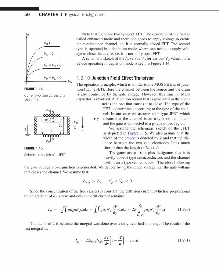
�0 CHAPTER � Physical Background
Note that there are two types of FET. The operation of the first is called enhanced mode and there one needs to apply voltage to create the conductance channel, i.e. it is normally closed FET. The second type is operated in a depletion mode where one needs to apply volt-age to close the device, i.e. it is normally open FET.
A schematic sketch of the ID versus VD for various VG values for a device operating in depletion mode is seen in Figure 1.14.
1.2.10 Junction Field Effect TransistorThe operation principle, which is similar to the MOS FET, is of junc-tion FET (JFET). Here the channel between the source and the drain is also controlled by the gate voltage. However, this time no MOS capacitor is involved. A depletion region that is generated in the chan-
nel is the one that causes it to close. The type of the FET is determined according to the type of the chan-nel. In our case we assume an n-type JFET which means that the channel is an n-type semiconductor and the gate is connected to a p-type doped region.
We assume the schematic sketch of the JFET as depicted in Figure 1.15. We also assume that the width of the device is denoted by Z and that the dis-tance between the two gate electrodes 2a is much shorter than the length L: 2a << L.
The gates are p+ (the plus designates that it is heavily doped) type semiconductors and the channel itself is an n-type semiconductor. Therefore following
the gate voltage a p–n junction is generated. We denote by Vp the pinch voltage, i.e. the gate voltage that closes the channel. We assume that:
V V V VDsat D p G> < < 0
Since the concentration of the free carriers is constant, the diffusion current (which is proportional to the gradient of n) is zero and only the drift current remains:
I q nE x z q NV
yx z Z q N
V
yxD n y n d n d
W y
a
= − = =∫∫ ∫∫ ∫ d dd
dd d
d
dd2
( )
(1.290)
The factor of 2 is because the integral was done over x only over half the range. The result of the last integral is:
I Zq N a
V
y
W
aconstD n d= −
=2 1
d
d (1.291)
VD
Vth = VG < 0
Vth < VG < 0
VG = 0
VG > 0
ID
FIgURE 1.14
Current–voltage curves of a MOS FET.
D
G
S
G
y
xL
w(y)
2a+VD
VG
VG
FIgURE 1.15
Schematic sketch of a JFET.
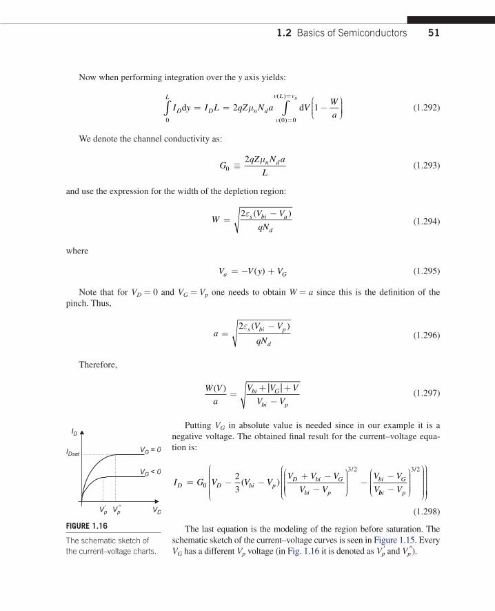
��
Now when performing integration over the y axis yields:
I y I L qZ N a VW
aD D n d
v
v L vL D
d d= = −
=
=
∫∫ 2 10 00
( )
( )
(1.292)
We denote the channel conductivity as:
G
qZ N a
Ln d
02
≡
(1.293)
and use the expression for the width of the depletion region:
WV V
qNs bi a
d
=−2ε ( )
(1.294)
where
V V y Va G= − +( ) (1.295)
Note that for VD = 0 and VG = Vp one needs to obtain W = a since this is the definition of the pinch. Thus,
aV V
qNs bi p
d
=−2ε ( )
(1.296)
Therefore,
W V
a
V V V
V Vbi G
bi p
( )=
+ +−
| |
(1.297)
Putting VG in absolute value is needed since in our example it is a negative voltage. The obtained final result for the current–voltage equa-tion is:
I G V V VV V V
V V
V V
VD D bi pD bi G
bi p
bi G= − −+ −
−
−
−0
3 22
3( )
/
bbi pV−
3 2/
(1.298)
The last equation is the modeling of the region before saturation. The schematic sketch of the current–voltage curves is seen in Figure 1.15. Every VG has a different Vp voltage (in Fig. 1.16 it is denoted as Vp
′ and Vp″).
VD
VG < 0
VG = 0
ID
IDsat
Vp′ Vp
″
FIgURE 1.16
The schematic sketch of the current–voltage charts.
�.� Basics of Semiconductors

�� CHAPTER � Physical Background
Note that in the case of a p-type JFET a similar equation to the one of Eq. 1.298 is obtained. In this case though Vp, VG are positive and VD is negative. For a p-type JFET one has:
I G V V VV V V
V V
V V
VD D bi pG bi D
bi p
bi G= + ++ −
+
−
+0
3 22
3( )
/
bbi pV+
3 2/
1.3 INTRODUCTION TO PHOTONIC WAvEgUIDINgIn this subsection we will review the basic properties of guiding light in photonic structures.
1.3.1 Waveguide ModesFrom Maxwell equations under the assumption of a monochromatic wave with temporal dependency of exp(it) the wave equation is obtained:
∇ + =2 20
2 0E n k E (1.299)
where n is the refractive index, k0 = /c with c being the speed of light and the radial frequency of the radiation. Assuming a symmetric waveguide as depicted in Figure 1.17 with ∂/∂y = 0, the solu-tion for the field is:
E r E x i z( ) ( ) exp( )= −
(1.300)
where is a constant which need not yet be found.This results in the following wave equation:
∂
∂+ − =
2
22
02 2 0
E
xn k E( )
(1.301)
The next step is solving the differential equation in each one of the three regions (the refractive index n is changed between the regions) and applying the boundary conditions. Assume a TE (transverse elec-tric) polarization mode, i.e. E is polarized towards the y direction:
E
A p x d i z x d
B hx i z x dy =− − − >
− <
exp[ ( ) ]
cos( )exp( )
| | | |
| |
(1.302)
x = d
x = −d
n2
n1
n1
z
x
FIgURE 1.17
Symmetric waveguide.

��
and the solution for Hz is:
Hi E
x
ipA p x d i z x d
ihB hx
zy=
∂
∂=
− − − >
−−
exp[ ( ) ]
sin( ) exp(
| | | |
ii z x d ) | | <
(1.303)
Our boundary conditions should be the continuity of the fields and thus one obtains:
A B hdpA hB hd
==
cos( )sin( )
(1.304)
The solution is:
p h hd= tan( )
(1.305)
where
202
22 2
202
12 2
= − <= + >
k n h x d
k n p x d
| |
| |
(1.306)
which yields:
p h n n k2 222
12
02+ = −( )
(1.307)
Finding the solution for p and h can be found graphically using Eqs. 1.305 and 1.307 (i.e. the intersection between two curves of tangent function and a circle) as depicted in Figure 1.18.
One may define the radius as:
V d p h d n n k= + = −2 2
22
12
0 (1.308)
A single-mode solution is obtained for V < /2.The effective refraction index is:
n
keff =
0 (1.309)
while the equation relating to k0 is called the dispersion equation. A similar solution can be found for Hy in the TM (transverse mag-netic) polarization mode.
Assume now an asymmetric waveguide as depicted in Figure 1.19.Assume n = n(x) and ∂/∂y = 0 while the propagation is towards
the z direction. For the TE mode one obtains the Helmholtz wave
hd
pd
π/2 π
TE0 TE1
FIgURE 1.18
Finding the guided modes.
�.� Introduction to Photonic Waveguiding
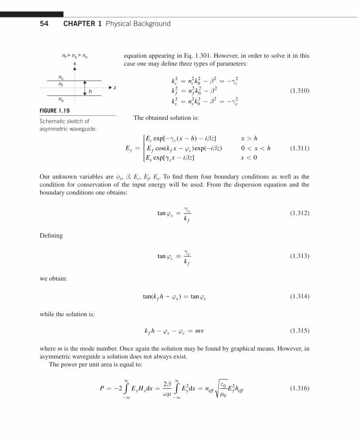
�� CHAPTER � Physical Background
equation appearing in Eq. 1.301. However, in order to solve it in this case one may define three types of parameters:
k n k
k n k
k n k
c c c
f f
s s s
2 202 2 2
2 202 2
2 202 2 2
= − = −= −
= − = −
γ
γ
(1.310)
The obtained solution is:
E
E x h i z x h
E k x i z x h
Ey
c c
f f s
s
=− − − >
− − < <exp[ ( ) ]
cos( )exp( )
exp[
γ ϕ 0
γγ s x i z x− <
] 0
(1.311)
Our unknown variables are s, , Ec, Ef, Es. To find them four boundary conditions as well as the condition for conservation of the input energy will be used. From the dispersion equation and the boundary conditions one obtains:
tanϕγ
ss
fk=
(1.312)
Defining
tanϕγ
cc
fk≡
(1.313)
we obtain:
tan( ) tank hf s c− =ϕ ϕ
(1.314)
while the solution is:
k h mf s c− − =ϕ ϕ
(1.315)
where m is the mode number. Once again the solution may be found by graphical means. However, in asymmetric waveguide a solution does not always exist.
The power per unit area is equal to:
P E H x E x n E hy x y eff f eff= − = =−∞
∞
−∞
∞
∫ ∫22 2 0
0
2d d
ε
(1.316)
nf > ns > nc
z
x
nf
h
nc
ns
FIgURE 1.19
Schematic sketch of asymmetric waveguide.

��
where heff is the effective width of the mode:
h heff
s c
= + +1 1
γ γ (1.317)
1.3.2 Longitudinally Perturbed WaveguideWe assume that the solution has the form of:
E x y z t A z E x y i t i zm m mm
( , , , ) ( ) ( , ) exp( )= −∑
(1.318)
It is needed to find the coefficients Am. We start from the wave equation with perturbation over the dielectric constant:
[ ( ( , ) ( , , ))]∇ + + =2 2 0 ε εa x y x y z E
(1.319)
Note that by Em we denote the solution for the wave equation without the longitudinal perturbations:
E x y z t E x y i t i zm m( , , , ) ( , ) exp( )= −
(1.320)
and the relevant wave equation is:
[ ( , ) ] ( , )∇ + − =2 2 2 0 ε a m mx y E x y
(1.321)
assuming orthogonal modes:
E x y E x y x yn m
mmn( , ) ( , )d d
| |=∫
2δ
(1.322)
where
δmn
m n
m n=
=≠
1
0 (1.323)
Substituting Eq. 1.318 into Eq. 1.319 and assuming slow varying amplitude, i.e.:
d
d
d
d
2
2
A z
z
A z
zm
mm( ) ( )
<<
(1.324)
�.� Introduction to Photonic Waveguiding

�� CHAPTER � Physical Background
we obtain after using the relation of Eq. 1.225 the following:
− − = −∑2 2i E x yA z
zi z x y z A z E x ym m
mm
mn n ε( , )
( )exp( ) ( , , ) ( ) ( , )
d
d eexp( )−∑ i zn
n
(1.325)
Denoting the overlapping integrals as follows (using the orthogonality property of Eq. 1.322):
E E x y k k
E x y z E x y k n
k kk
k n
d d| |
d d | |
= ≡< >
≡< >
∫
∫
2
ε ε
|
( , , )
(1.326)
we obtain:
2
2
2
ε | |
d
d
d
d| |
k
k k
kn k
A z
zk k
A z
z ik n A z i z
( )|
( )( )exp(=< > = < > −−∑ i zn
n
)
(1.327)
We now decompose ε to Fourier series:
ε ε = −≠
∑ mm
x y imz( , ) exp( )20
/
(1.328)
where is the longitudinal periodicity of the perturbation. Substituting Eq. 1.328 into Eq. 1.327 we obtain:
d
d | |
A z
zi c A z m zk k
kknm
nn
k n( )
( )exp= − − −
∑
2
≠∑m 0
(1.329)
where
C k x y nkn
mm≡ < >
ε
4| |( , )
(1.330)
Longitudinal phase matching is obtained when:
= − − =k n m
20
(1.331)
When there are two modes in the same direction one obtains from Eqs. 1.329 and 1.330 that:
d
dd
d
A
ziC A z i z
A
ziC A z i z
m
m
112 2
212 1
= −
= − −
( )exp( )
( )exp( )
(1.332)

��
Due to energy conservation one has:
d
d| | | |
zA A1
22
2 0+( ) =
(1.333)
and in the case of phase matching:
d
dd
d
A
ziC A z
A
ziC A z
m
m
112 2
212 1
= −
= −
( )
( )
(1.334)
The solution of the differential equation is:
A z A C z iA C zm m1 1 12 2 120 0( ) ( ) cos( ) ( )sin( )= −
(1.335)
For two modes in opposite directions one similarly has:
d
dd
d
A
ziC A z i z
A
ziC A z i z
m
m
112 2
212 1
= −
= −
( )exp( )
( )exp( )
(1.336)
and an energy conservation relation of:
d
d| | | |
zA A1
22
2 0−( ) =
(1.337)
From those equations one may easily extract and understand the solution for the modes evolved in the optical waveguide.
References [1] R.W. Boyd, Nonlinear Optics, Academic Press, San Diego, 2003. [2] A. Yariv, P. Yeh, Optical Waves in Crystals: Propagation and Control of Laser Radiation, John Wiley & Sons
Inc., 2002. [3] M. Zambuto, Semiconductor Devices (Electronics and Electronic Circuits), McGraw-Hill College, 1989.
References

59Integrated Nanophotonic Devices. DOI:© 2010 Elsevier Inc. All rights reserved.
10.1016/B978-1-4377-7848-9.00002-12010
CHAPTER OUTLINE HEAD
2.1 Magneto-Optic Modulators ................................................................................................................592.2 Electro-Optic Modulators ...................................................................................................................60
2.2.1 TheElectro-OpticKerrEffect...................................................................................... 602.2.2 PockelsElectro-OpticalEffect..................................................................................... 62
2.3 Liquid Crystals ..................................................................................................................................622.3.1 HomogeneouslyAlignedNLCs..................................................................................... 632.3.2 TwistedNematicLCs.................................................................................................. 652.3.3 CLCs........................................................................................................................ 652.3.4 FLCs........................................................................................................................ 66
2.4 Electro-Absorption ............................................................................................................................662.5 Non-Linear Optics .............................................................................................................................67
2.5.1 TheACKerrEffect................................................................................................... 672.5.2 PhotorefractiveEffects............................................................................................... 672.5.3 FrequencyMixing...................................................................................................... 68
2.6 Raman and Brillouin Effects ...............................................................................................................692.6.1 RamanAmplification.................................................................................................. 692.6.2 BrillouinScattering.................................................................................................... 69
2.7 Plasma Effect in Silicon ....................................................................................................................702.8 Overview of Photonic Devices ............................................................................................................70References ..............................................................................................................................................73
Physics of Optical Modulation 2CHAPTER
In this chapter a mini review is given to introduce the main physical effects that are used in order to generate photonic modulators. We will refer to those effects in the following sections, where the oper-ation principle of specific devices is to be discussed. Some of the effects that will be discussed here are more relevant or more applicable than others to be used in integrated photonic circuits.
2.1 MAgNETO-OPTIC MODULATORSThe magneto-optic (MO) effect, known also as the Faraday effect, is the creation of circular birefrin-gence (CB) in a medium due to an applied magnetic field [1,2]. A material has CB when right cir-cular polarization (RCP) and left circular polarization (LCP) experience different refractive indices. As shown by Faraday and many others later on, there exists a wide group of materials that exhibit a significant MO effect. These are called magneto-optic materials.

60 CHAPTER 2 Physics of Optical Modulation
In order to get CB in MO materials one usually (except when there is natural CB) needs to apply a magnetic field parallel to the wave’s direction of propagation. Let us denote the refractive index dif-ference caused due to the magnetic field B by:
n B n n( ) = −− + (2.1)
where n+ and n− are the refractive indexes for RCP and LCP, respectively.An important property of the MO effect is that it leads to polarization rotation of any arbitrary
linearly polarized wave propagating through the CB medium. Suppose a wave is propagating in a CB medium. If the incident field is linearly polarized then it can be decomposed into RCP and LCP com-ponents, which after propagation distance z each will accumulate a different phase 2π zn± / so one can write:
EE
e ie i t n z e ie i t n zx y x y= − − + + −+ −0
022 2( ) [ ( / ) ( ) [ ( exp exp π π // )
( )
π δ δ
0
0 022 2
= −[ ] +
E i t nz e ex yexp / cos sin (2.2)
where 0 is the free space wavelength, n n n= ++ −( )/2 is the average index and the circular phase retardation is:
δ π = 2 0nz/ (2.3)
It is apparent from the last two equations that propagation in the CB medium leads to polarization rotation by δ /2 . Devices that create polarization rotation based on the MO effect are called Faraday rotators. We should note that n will be positive or negative depending on whether the direction of the induced magnetic field is with or against the wave’s direction of propagation, respectively. This directional property of the MO effect makes the Faraday rotators non-reciprocal devices, which are very useful for applications such as optical isolation and optical modulation.
2.2 ELECTRO-OPTIC MODULATORS2.2.1 The Electro-Optic Kerr EffectTwo Kerr effects can be distinguished: (i) the Kerr effect applied at low frequencies, which is also called the DC Kerr effect and whose main application is electro-optical modulators [3–5], and (ii) the AC Kerr effect applied at high frequencies (e.g., the frequencies of the light itself), whose main appli-cation is for non-linear optics, i.e., all-optical interaction [6,7].
In the DC Kerr effect an external electrical field is slowly varying (at frequencies that are much lower than the frequency of the visible light) and induces birefringence in the material. The change in the index of refraction is proportional to the square of the external electric field and it is induced along the axes that are parallel or perpendicular to the direction of the applied field. Mathematically,
n = EDC2 , (2.4)

61
where n is the change in the refractive index, is a constant, is the optical wavelength in the material, and EDC is the external electrical DC field. The physical reasoning for this effect is as fol-lows. The electric polarization in a medium can be expressed as a power series of the field’s compo-nents as follows:
P E E El lj jj
ljkk
j kj
ljkmm
= + += == =
ε ε ε 01
1
3
02
1
3
1
3
03
1
3( ) ( ) ( )∑ ∑∑ ∑
kkj k m
j
E E E==
+1
3
1
3
∑∑ ... (2.5)
where ε0 is the vacuum permittivity and (n) is the nth order component of the electric susceptibility of the material. The indexes designate the vector components over the three main axes (x, y and z). For materials exhibiting a non-negligible Kerr effect, the third term that is proportional to (3) is not negligible, with the even-order terms typically dropping out due to inversion symmetry of the Kerr medium. Assuming that an external electric field is applied, we have
E t E E t( ) ( ),= +0 cos (2.6)
where is the radial frequency of the varying electric field. Then the electric polarization components (for x, y and z) become:
P E E t E t= +( ) =ε ε 0
1 30
203( ) ( ) | | cos( ) cos( ) (2.7)
This is for a material in which all the components of are equal. Therefore, since the refractive index n is related to the permittivity we obtain
n EE
= + = + + = + ⋅ ++
1 1 3 1 13
11 3
02 1
30
2
1
( ) ( ) ( )
( )
( )| |
| | (2.8)
Since (1) (3) we can perform Taylor expansion for the square root of Eq. 2.8 and obtain
nE
nno≈ + ⋅ +
+( )
= +1 1
3
2 1
3
21
30
2
1
3
( )( )
( )
( )| |
oo
E| | ,02 (2.9)
with n0 as the refractive index in the material when no external field is applied. Note that
no = +1 1( ) (2.10)
Therefore the refractive index change is indeed proportional to the square of the DC electric field as indicated in Eq. 2.4.
The induced birefringence can rotate the polarization of the incoming light. If the material is placed between two orthogonal polarizers, the polarization modulation can be translated into ampli-tude modulation. This is the fundamental principle of operation for electro-optical modulators based
2.2 Electro-Optic Modulators

62 CHAPTER 2 Physics of Optical Modulation
upon the Kerr effect. One example of Kerr material used for electro-optical modulation is PLZT [4,8]. The Kerr effect can reach high-modulation frequencies of several GHz, but, since is small, it usu-ally requires high fields in order to obtain high-contrast modulation. Therefore, in many cases, the electronic capabilities are the major limiting cause for the overall operation rate.
2.2.2 Pockels Electro-Optical EffectThis effect is used in order to construct Pockels cells or electro-optical modulators based upon the Pockels effect [9,10]. In this case the relevant expression is related to the coefficient of (2) and the change in the refractive index is proportional to the applied DC electric field rather than the square of its magnitude. The induced birefringence occurs only in materials that lack inversion symmetry such as LiNbO3, BBO, and GaAs.
2.3 LIqUID CRySTALSThere are many thermotropic phases of liquid crystals (LCs); in Figure 2.1 we present some of the important ones [11,12]. The main types of liquid crystals important for modulation are: nematic LCs (NLCs), cholesteric LCs (CLCs), and ferroelectric LCs (FLCs). Note that when the molecules are
chiral (lacking mirror symmetry) the resulting struc-ture is helicoidal due to the twisting forces between neighboring molecules resulting from the chiral inter-action. The alignment geometry of the LC molecules and their anchoring conditions on the substrates also play an important factor in the structure of the device. By homeortropic alignment we mean the molecules on the surfaces are perpendicular to the substrate plane while the homogeneous alignment means the molecules on the surfaces are lying in the substrate plane or inclining at a small angle with the plane. Liquid crystals exhibit large electro-optic effects due to the molecular coupling with an applied electric field which can be dielectric coupling or ferroelectric coupling. Due to their rod-like shape, LC molecules possess dielectric anisotropy ε ε ε= − ⊥|| because the dielectric constants parallel, ε|| , and perpendicu-lar, ε⊥, to their long axis are different. This is true both in the DC regime and in the optical regime, thus they also possess strong optical birefringence: n n n= − ⊥|| where n n|| || ;= =⊥ ⊥ε ε typi-cally ranging from 0.1–0.3 and for some LC mixtures it can be as high as 0.5. In the dielectric coupling a torque is acting on the molecules and trying to rotate them parallel to the applied field if their dielectric
Nematic(N)
Smectic A(SmA)
Chiral nematicCholesteric(N* or CLC) Chiral smectic C
(SmC*)
P
PP/2
P/2
Smectic C(SmC)
FIgURE 2.1
Schematic of the main thermotropic phases. In the nematic, SmA and SmC phases the structure is uniform while in the CLC and SmC* phases the structure is helicoidal.

63
anisotropy is positive and perpendicular to the field if their dielectric anisotropy is negative. Because the dielectric coupling is associated with induced dipole moment, the coupling depends on the applied voltage as V 2 and therefore the molecules do not distinguish the sign of the field. In the ferroelectric LC phase [13] the molecules possess a spontaneous dipole moment and therefore the molecules tend to align parallel to the field. In the antiferroelectric LC phase the molecules tend to align antiparallel to the field. The ferroelectric and antiferroelectric coupling energies are linear with the applied field and therefore in these cases the molecules do respond to the applied field. Upon applying an electric field the rod-like molecules can rotate by a large angle depending on the mate-rial, the surface anchoring conditions and the LC phase itself. The net result could be a deformation of the anisotropic structure, pure rotation of the optic axis or pure variation of the effective birefrin-gence, which in the end result in a strong electro-optical effect. The deformed structure is a result of the balance between the electric and elastic forces as well as the anchoring of the molecules to the boundaries.
Applications of LCs in integrated devices are numerous but we mention filling hollow-core fibers and by that realizing long-period gratings [14] where the periodically poled LC produces an index modulation in the core according to the poling direction. The long-period structure couples between the fundamental core mode and the leaky cladding modes. The generation of tunable structures has many applications in optical communications [15], such as gain flattening filters, band rejection fil-ters, and variable optical attenuators [16–18]. Photonic crystal band-gap structures were filled with nematic LCs and used as modulation devices [19–21]. In what follows we describe in more detail some of the important LC device geometries, particularly the homogeneously aligned LC device as it is the basis for many LC devices.
2.3.1 Homogeneously Aligned NLCsIn their homogeneous geometry shown in Figure 2.2 the LC molecules are parallel to the substrate plane. The substrates are coated with transparent conducting oxide (TCO) layers and then with nanometer scale (10–30 nm) thick alignment layers usually made of polymers or polyimides. In the mechanical rubbing alignment the alignment layers are rubbed unidirectionally with a special cloth. In the UV alignment the polymer is selected to be sensitive to polarized UV irradiation which pro-duces some unidirectional alignment to the LC molecules.
Upon applying an electric field perpendicular to the substrates the dielectric torque generated on a molecule with positive dielectric anisotropy tends to align it in parallel to its direction; however, the elastic forces and the anchoring of the molecules at the boundaries result in a deformed structure [22]. The structure deformation is presented schematically in Figure 2.2C in which the molecules remain oriented in the xz plane, that is no twist generated. In referring to Figure 2.2B, for light propagating normal to the substrate plane the ordinary and extraordinary indices are given by:
n n n V zn n
n n n V zo e= =
− −⊥
⊥
⊥
; ( ( , ))( ) ( , )
||
|| ||
cos
θθ2 2 2 2
(2.11)
The molecules tilt angle θ( , )V z is a function of both the applied voltage and the distance between the plates. An example of such a non-uniform profile is shown in Figure 2.2C and schematically in
2.3 Liquid Crystals

64 CHAPTER 2 Physics of Optical Modulation
Figure 2.2D. Since the profile is changing gradually then the phase retardation accumulated by pass-ing through the device is:
Γ( ) ( ( ( , )) )V n V z n ze o
d
= −∫2
0
π
θ d (2.12)
HNLC geometry is an important and commonly used geometry in LC devices as phase, polariza-tion and intensity modulators. When pixelated they are used as spatial light modulators (SLMs). They
ε
k
TCOelectrodes
(A) (B)
(C)
90
80
70
60
50
40
30
20
10
0.5
0.75
1
1.25
1.5
1.75
2 2.53
46
00.0 0.2 0.4
Z/d
Mol
ecul
es ti
lt a
ngle
(de
g)
0.6 0.8 1.0
(D)
X
Z
θ φ
ZT
ilt a
ngle
Alignmentlayers
Glass
Glass
ε⊥
ε||
FIgURE 2.2
(A) Cross-section of homogeneously aligned NLC device (HNLC). (B) Molecule orientation and principal axis of the dielectric tensor. (C) Simulated tilt angle profiles as function of the distance between the plates normalized to the LC thickness at different voltages when the molecules at the boundaries are titled initially at 10 degrees and the surface anchoring energy is 0 84. J/m2. The voltages are normalized to Frederick’s threshold voltage. (D) Schematic illustration of the non-uniform molecule profile under an applied field.

65
exhibit large phase retardation because the effective extraordinary index varies from nearly n|| at zero voltage to nearly n⊥ at high enough voltage (typically 10 volts at a few hundred Hz is adequate). One of the important advantages of the HNLC geometry is the ease of preparation and alignment quality that can be easily achieved. As tunable retardation plates many other devices can be built by stacking several together such as Lyot and Solc type filters [23–25] as well as polarization controllers [26] and rotators [27,28]. They were used as photonic tunable narrowband filters in resonant guided wave structures [29,30]. Tunable Fabry–Perot filters have also been demonstrated with the advantage of being miniature and fast as only a single thin layer is needed [31,32] and possibility of obtaining polarization independence in a single device was also proposed [33,34]. LCs in the HNLC geometry were shown to be useful devices for the microwave [35] and THz range [36,37] as well, since their birefringence was found to be high enough to build devices with reasonable thickness.
2.3.2 Twisted Nematic LCsTwisted nematic LCs (TNLCs) are formed when the azimuthal angle in Figure 3.2B is fixed at the first boundary to φ = 0 while at the upper boundary it is fixed at φ = °90 . As result a twisted struc-ture is formed where the twist angle changes linearly with z: φ = πz d/2 . The optical properties of such structure are based on a phenomenon called the adiabatic following valid under the condition of small twist rates: π π / /2 2 Γ = d n which is easily satisfied for device thicknesses of 5–10 microns in the visible range. In this case light that is impinging at normal incidence and polarized along one of the principal axes of the molecules at the first boundary remains linearly polarized and follows the rotation of the molecules thus exiting the device rotated by the total twist of π /2 . Hence extinction is obtained when the device is between crossed polarizers. Upon applying an electric field the structure deforms and the light starts to leak through until at high enough voltage a bright state is achieved. The deformation of TNLCs is more complicated than the HNLC case because two elastic deformations occur in the two angles φ,θ . TNLCs are being used in LC displays (LCDs) as well as in other photonic devices such as modulators [38], achromatic polarization controllers and rotators [39], achromatic waveplates [40] and tunable filters [41,42].
2.3.3 CLCsThe CLCs are materials having molecules organized in a helical structure exhibiting selective reflec-tion properties in a similar manner to Bragg grating. Due to the anisotropy they have the ability to reflect light at a specific wavelength when aligned in a planar texture and the incident light is circu-larly polarized with the same helicity as the cholesteric helix. This configuration is obtained when no external field is applied over the material. Small electric fields cause deformation of the helix, increase in the pitch and so tunability of the reflection band is obtained. Scattering can take place from the focal conic texture that can develop upon applying a field in polymer-dispersed CLCs [43]. CLCs in Fabry–Perot cavity have also been considered and showed unique characteristics includ-ing polarization-independent operation [44]. As a photonic crystal material, CLCs have been used as hosts to enhance the lasing efficiency when the laser is operating at a wavelength near the reflection band edge where the photon density of states is enhanced [45,46]. The CLC laser is formed by doping with dye molecules that can emit at the wavelengths near the stop band with no need for external mirrors. Short pitch CLCs when aligned so that their helix direction is in the plane of the substrate
2.3 Liquid Crystals

66 CHAPTER 2 Physics of Optical Modulation
exhibit an additional phenomenon called flexoelectricity, an effect that provides fast switching and is being considered for display applications [47].
2.3.4 FLCsIn FLCs [48] the molecules possess spontaneous polarization P and therefore the major coupling is due to the linear interaction with the applied field
P E⋅ . In chiral smectic C (SmC*) phase, the sym-
metry hinders the spinning of the molecules around their long axis and as a result a spontaneous dipole moment appears. However, because the structure is helicoidal the net spontaneous polarization aver-ages zero. Upon applying an electric field perpendicular to the helix direction the structure deforms and several electro-optic effects arise. This can be easily achieved by having the helix aligned parallel to the substrates plane. When the pitch is longer than the wavelength, diffraction takes place, which then can be modulated by the applied voltage. When the pitch is much smaller than the wavelength there is no diffraction and the medium behaves as a uniaxial plate. Applying a voltage then causes nearly linear rotation of the optic axis. This mode of FLCs is called distorted helix ferroelectric (DHF) mode [49].
When the SmC* phase is aligned so that the helix direction is in the substrates plane and the pitch is large enough compared to the device thickness, the helix unwinds and bulk spontaneous polariza-tion appears in what is called the surface stabilized ferroelectric LC (SSFLC) geometry. In the SSFLC geometry the molecules are arranged in layers in what is called the bookshelf geometry in which the layers are arranged like books perpendicular to the substrates. Applying the field between the sub-strates produces rotation of the optic axis in the plane of the substrates, hence the optical modulation is caused by the rotation of the optics axis and not modulation of the birefringence. Their main advan-tage over NLCs and CLCs is the low voltage required and the high speed reaching microseconds switching times as compared to ms scale in the case of NLCs and CLCs.
Antiferroelectric (AFLC) phases were also found recently to exhibit unique optical properties when their tilt angle is close to 45 degrees [50,51] including linear electro-optic response, high con-trast and fast response time.
Liquid crystals are rich in electro-optic effects, some of which are familiar in display applications, but there are others not used much in displays; however, their potential is huge in photonic devices and they are being explored continuously. Among these are the linear and fast electroclinic effect aris-ing due to the coupling between the tilt and the polarization [52,53], applications in waveguides, THz devices, microwave devices, adaptive lenses [54–56] and imaging applications [57]. Non-linear optics of liquid crystals is another field of ongoing interest due to the different phenomena rich in physics being explored and the interesting applications in all optical switching devices in optical telecommu-nications. Two active conferences are being held biannually: optics of liquid crystals (OLC) confer-ence and liquid crystal photonics (LCP) conference.
2.4 ELECTRO-ABSORPTIONThere are several physical effects related to absorption which is induced by applying an external elec-tric field on a material. In general, since these effects are very fast (ns–ps range), they are commonly used in optical communication for the realization of electro-optical modulators. The materials used for such modulators are usually InGaAsP allowing modulation rates of hundreds of GHz.

67
The first related effect is called the Franz–Keldysh effect [58,59] and it occurs in semiconduc-tors when the wave functions leak into the band gap of the crystal. When an external electric field is applied, the wave functions of the electron and the hole become Airy functions rather than regular plane waves. The Airy function distribution has tails that leak into the forbidden band gap. The more the overlap between the free electron and the free hole functions is, the stronger the leakage and con-sequently the induced attenuation (since the absorption spectrum now includes a tail at energies below the band gap as well as in those that are above it).
The electro-absorption due to the Stark effect is related to the shifting and splitting of spectral lines of atoms because of the presence of an external electric field. There are components of shifting and splitting that are proportional to the external fields while others have non-linearity and are pro-portional to the square of the field. It is the electric analog to the Zeeman effect in which the splitting is induced due to the presence of a magnetic field.
2.5 NON-LINEAR OPTICS2.5.1 The AC Kerr EffectWe may follow the mathematical derivation of Eqs. 2.5–2.10 while assuming that the term of E = E0cos(t) now has as the optical radial frequency:
P E E t E t= +
=ε ε 0
1 30
20 0 0
3
4( ) ( ) | | ( ) cos( )cos (2.13)
which leads to:
nE
nno≈ + ⋅ +
+( )
= +1 1
3
8 1
3
81
30
2
1
3
( )( )
( )
( )| |
ooo
o
E nn
I| |( )
02
33
8= +
(2.14)
where I is the light intensity. This effect can be used for the realization of an all-optical logic gate and other interesting devices for information processing [60].
2.5.2 Photorefractive EffectsThe photorefractive effect is a non-linear effect in which external light varies the refractive index of the material. This effect is commonly used for the generation of holographic gratings acting as tun-able filters and switches [61–63] or as wavelength converters [64]. The physical concept is related to the following: When a pattern of bright and dark fringes of light is generated in the crystal, the electrons in the bright regions absorb the light and jump from the valence band into the conduction band. The electrons are free to move in the crystal and since they were generated in the bright fringe they tend to diffuse towards the dark regions. Note that when the electrons are trapped they will not be able to move again (until they are re-excited with the light as before). With the net redistribution of electrons into the dark regions of the material, leaving holes in the bright areas, spatial charge dis-tribution is generated. This charge causes an electric field and, due to the electro-optic effect that was
2.5 Non-Linear Optics

68 CHAPTER 2 Physics of Optical Modulation
previously analyzed, it generates spatial variation of the refractive index. This periodic grating, which is made from a variation of the refractive index, can affect another light beam that will pass through the crystal. The pattern stored inside the crystal persists until this pattern is erased, which can be achieved by applying uniform illumination on top of it. Typical photorefractive crystals are BaTiO3 and LiNbO3 [65,66].
2.5.3 Frequency MixingWe observe again Eq. 2.5 and assume an optical field that is a combination of two terms, each having a different optical radial frequency of 1 and 2:
E r t E t k r E t k r
E i t ik r E
( , ) cos cos
exp
= − ⋅( ) + − ⋅( )
=− ⋅( ) +
1 1 1 2 2 2
1 1 1
22 2 2
2
exp. .
i t ik rc c
− ⋅( )
+
(2.15)
where c.c. stands for complex conjugate, r is the position vector, and k is the wave vector. Substituting this field into Eq. 2.5 and observing the second term of non-linearity yields
P r t P i t ik r c c
E E
( )
( ) ( ) (
( , ) exp . .20 3 3
212 2
22 22 2 2
= − ⋅( ) +∝ + +
))
( )
exp
exp
E E i t i k k r
E E i t i k
1 2 1 2 1 2
21 2 1 2 12
−( ) − −( ) ⋅( )+ +( ) − + kk r
E i t i k r
E i t i
2
212
1 1
22
22
2 2
2
( ) ⋅( )+ ( ) − ( ) ⋅( )+ ( ) −
( )
( )
exp
exp 22 2k r c c( ) ⋅( ) + . . (2.16)
Therefore, in the time domain, one may see that the radial frequency of the generated radiation 3 is equal to double that of the original radial frequencies as well as the sum and difference of the fre-quencies. In the case where both electric fields are the same, i.e., 1 = 2, then the output has a strong double-frequency component 3 = 21.
The phase-matching condition that is related also to the momentum conservation is extracted from the spatial axis and therefore the generated wave vector k3 is also equal to the sum and the differences of the wave vectors of the original fields. Since k n c3 3 3= ⋅( ) / (where c is the speed of light), the phase-matching condition is related also to the spectral dependence of the refractive index n.
Note that in this brief description we have considered only the second-order non-linearity related to (2). Higher order non-linearity such as (3) is responsible for effects such as self-phase modula-tion. Several types of all-optical logic gates and all-optical modulators as well as wavelength convert-ers that are used for optical communication are based upon these types of non-linear effects [67,68].
One interesting effect that is often used in optical devices is two-photon absorption (TPA) [69,70]. Assume a material such as a semiconductor in which the energy of a single photon is not sufficient in order to generate an electron–hole pair (to release an electron from the valence band into the conduct-ance band) and therefore the photon in that specific wavelength is not absorbed while passing through the semiconductor. The TPA effect occurs when two such photons are absorbed while the energy of both of them is now sufficient to release a free carrier electron (see Fig. 2.3).
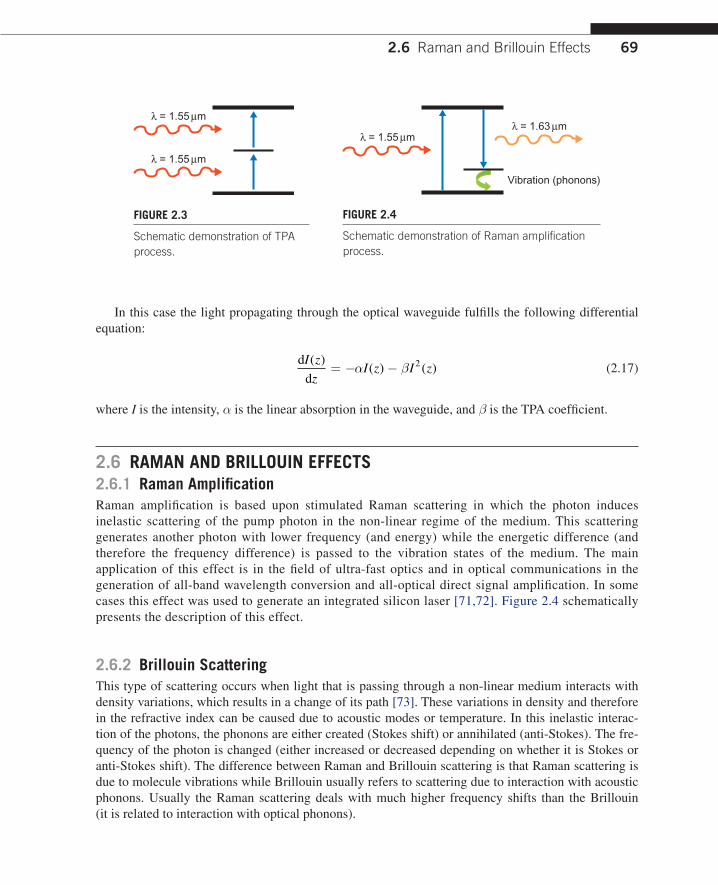
69
In this case the light propagating through the optical waveguide fulfills the following differential equation:
d
d
I z
zI z I z
( )( ) ( )= − − 2 (2.17)
where I is the intensity, is the linear absorption in the waveguide, and is the TPA coefficient.
2.6 RAMAN AND BRILLOUIN EFFECTS2.6.1 Raman AmplificationRaman amplification is based upon stimulated Raman scattering in which the photon induces inelastic scattering of the pump photon in the non-linear regime of the medium. This scattering generates another photon with lower frequency (and energy) while the energetic difference (and therefore the frequency difference) is passed to the vibration states of the medium. The main application of this effect is in the field of ultra-fast optics and in optical communications in the generation of all-band wavelength conversion and all-optical direct signal amplification. In some cases this effect was used to generate an integrated silicon laser [71,72]. Figure 2.4 schematically presents the description of this effect.
2.6.2 Brillouin ScatteringThis type of scattering occurs when light that is passing through a non-linear medium interacts with density variations, which results in a change of its path [73]. These variations in density and therefore in the refractive index can be caused due to acoustic modes or temperature. In this inelastic interac-tion of the photons, the phonons are either created (Stokes shift) or annihilated (anti-Stokes). The fre-quency of the photon is changed (either increased or decreased depending on whether it is Stokes or anti-Stokes shift). The difference between Raman and Brillouin scattering is that Raman scattering is due to molecule vibrations while Brillouin usually refers to scattering due to interaction with acoustic phonons. Usually the Raman scattering deals with much higher frequency shifts than the Brillouin (it is related to interaction with optical phonons).
λ = 1.55 µm
λ = 1.55 µm
FIgURE 2.3
Schematic demonstration of TPA process.
Vibration (phonons)
λ = 1.55 µmλ = 1.63 µm
FIgURE 2.4
Schematic demonstration of Raman amplification process.
2.6 Raman and Brillouin Effects

70 CHAPTER 2 Physics of Optical Modulation
2.7 PLASMA EFFECT IN SILICONPhotons that illuminate silicon and have energy (proportional to their frequency) that is larger than the band gap of this semiconductor may be absorbed in the material. Their absorption will release pairs of electrons and holes. Those mobile electrons and holes will affect the refractive index n and the absorption coefficient of the silicon [74] for light at different wavelengths which in the absence of this external illumination is not absorbed while guided through the device. The empirical relation is as follows:
= + = × + ×
= + = − × +
− −
−e h
e h
N P
n n n N
8 5 10 6 10
8 8 10 8
18 18
22
.
. .55 10 18 0 8× ( )
− P. (2.18)
where e[cm−1] is the absorption coefficient due to N[cm−3] (the change in the mobile electrons concentration), h[cm−1] is the absorption coefficient due to P[cm−3] (the change in the mobile holes concentration), n is the change in the refractive index, ne is the refractive index change due to electron concentration change, and nh is the refractive index change due to hole concentration.
This effect is commonly used in silicon in order to realize all-optical as well as electro-optical modulators and integrated devices [75,76].
2.8 OvERvIEw OF PHOTONIC DEvICESThere is a large variety of techniques for obtaining tunable filters, attenuators, switches, and other devices. Some technologies can become integrated circuits and some cannot. Previous works done on the design of optical tunable filters suggested a variety of different ways of implementation. The characteristics of the different filter designs are defined by their transmission bandwidth, suppression of side lobes, optical power loss, tuning power consumption, switching speed, size, and cost. Those filter designs include electro-optic devices [77–81], acousto-optic devices [82–85], ferro-electric liq-uid crystal devices [86]. The electro-optic devices are usually based on a cavity of an electro-optic material inserted into known filters such as the Fabry–Perot etalon, the Lyot filter, or the Šolc filter [87]. The tunability of those filters is achieved by applying an electrical voltage on the electro-optical material and changing the optical properties of the cavity. The change in the optical properties results in a change in the wavelength for which the filter achieves its peak transmittance.
The acousto-optic devices for modulation, filtering or switching are based on couplings of light from one optical mode to another or from one polarization mode to another due to interaction between the optical and the acoustic waves. The interaction medium can be an optical fiber [88–91] or fiber-compatible components such as GRIN lenses [92,93] or a bulk device [94–96], or it can be used as an optical beam deflector [97]. A change in the acoustic wave frequency and modulation will change the coupling between the different optical modes and will achieve the desired tunability for those devices.
Another device that was recently proposed is a device based upon the Lyot filter architecture with the addition of ferroelectric crystals along with the birefringent elements inside the filter’s cavity [98]. The ferroelectric liquid crystals act as a birefringent element with a varying optical axis, and the change in the optical axis of the element changes the design of the Lyot filter and results in different

71
wavelengths for the peak transmittance (see Ch. 1). The main advantage of the fer-roelectric crystals is that the applied elec-trical voltage is used only for switching between the two different optical states.
Another approach, which is more suit-able for integrated optics, is related to a realization of variable optical attenuators (VOAs) where the tuning mechanism is based upon thermal effects [99,100]. The VOA is an applicable component for optical communication applications. Here, an opti-cal waveguide is generated by ion exchange technology in glass. The ion exchange gen-erates the refractive index difference capable of guiding the light in the glass substrate. By creating a Mach–Zehnder interferometer (MZI) having heating electrodes positioned near one of the arms of the MZI, one may control the interference obtained in the out-put of the device. A schematic sketch of the device is presented in Figure 2.5.
Note that as part of the work in which integrated modulators were realized by tuning one arm of the MZI, periodically segmented waveguides were used as well [101]. As shown in Figure 2.6, these waveguides have a refractive index difference of n and a duty cycle of . They act as continu-ous waveguides with an index difference of n and a radiation loss factor that is a function of the waveguide parameters. The generation of such waveguides in Ti:LiNbO3 allowed for the creation of waveguides with controllable parameters for light guiding and with the potential capability for tun-ability using the non-linear as well as the electro-optic effects of the LiNbO3.
Switches are devices having more general functionality than modulators or VOAs. There are vari-ous approaches of using the electro-optical effect in order to realize switches: for instance, usage of the electro-optical effect of LCs [102] or the electro-optic Kerr effect (DC effect) in PLZT [4,6] or the electro-optical effect in GaAs that was used for realizing optical packet switching in optical commu-nication networks [103]. Another example of switches that should be mentioned includes a voltage-controlled photorefractive effect in KLTN [62], which is used in order to realize free-space optical interconnection networks. Photo-refraction is further used to generate wavelength-selective photonic switches [104].
The same photorefractive effect is also used for holographic memory with high storage density. For instance, in Refs [105,106] it is theoretically analyzed and then experimentally demonstrated with LiNbO3. Note that, as mentioned before, LiNbO3 is a material that is widely used as a modulator in optical communication applications [107].
Various integrated photonic devices such as multiple-quantum-well semiconductor devices as semiconductor optical amplifiers (SOA) can be used for electro-optical modulation and amplifica-tion of DWDM channels in optical communication (e.g., in Ref. [108] an amplification of 14 DWDM
MZI
Heating electrodes
Glass substrate
FIgURE 2.5
Thermally tuned MZI.
∆n
Λ
ηΛ
FIgURE 2.6
Periodically segmented waveguides.
2.8 Overview of Photonic Devices
72 CHAPTER 2 Physics of Optical Modulation
channels is demonstrated). However, these devices also exhibit non-linear effects that can be used for all-optical modulation, switching, and wavelength conversion. For instance, wavelength conversion that is based upon the principle of four-wave mixing in SOAs was demonstrated in Refs. [109,110]. All-optical switching that is based upon non-linear polarization rotation may be seen in Ref. [111] and all-optical logic gates in Ref. [112].
Vertical-cavity surface-emitting lasers (VCSELs) were another very important milestone in the development of integrated optical circuits. This device allowed for the generation of low-cost and fast (up to a few gigahertz) electrically modulated light sources. For instance, in Ref. [113] the authors investigate theoretically as well as experimentally the transverse light beam emitted from ring-shaped lasers such as VCSELs. Later on in Ref. [114] circular Bragg disk resonators are combined with VCSELs. This type of resonator [115] is schematically described in Figure 2.7.
Ring resonators can be used as tunable devices as well. For instance, in Ref. [116] the authors demonstrate the use of a set of two microscale ring resonators fabricated on a polymer substrate via soft lithography for realizing wavelength-selective response with suppressed side lobes. Tuning the spectral response was demonstrated using external illumination and a spectral shift of more than 2 nm was reported. The spectral shift was obtained by illuminating the polymer and inducing photobleach-ing, i.e., a change of its refractive index.
All-optical devices based upon Kerr non-linearity and soliton interactions play an important role in future development of photonic devices, although those approaches have not yet been proven as integrated concepts. For instance, in Ref. [60] the authors demonstrate the realization of a variety of logic operations by incoherent interactions of multiple spatial solitons with multilayered non-linear mediums having Kerr non-linearity. These approaches are well explained also in Ref. [117] where the authors generate 2-D discrete solitons in tunable photonic lattice structures (periodic structures that can be used for guiding light). The tunable lattice is created by using the Kerr non-linearity of the medium and after projecting beams from various directions (the interference pattern of the beams is the lattice). A schematic description of the system may be seen in Figure 2.8.
This is a good place to mention other non-linear effects such as two- and four-wave mixing, cross-phase modulation, Kerr non-linearity, the Raman effect, and electro-absorption, which are used for
Propagation direction
Bragg deflectors
Guiding defect
FIgURE 2.7
Circular Bragg disk resonators.
Illumination fromvarious directions
FIgURE 2.8
Two-dimensional optically induced non-linear photonic lattice.

73
the realization of optical dynamic devices such as switches, transistors, logic gates, and wavelength conversion [118–124].
An additional important trend that is worth mentioning here, and which probably will play an impor-tant role in the future development of integrated photonic multifunctional chips, is microfluidics. In microfluidics one is capable of integrating on a chip several devices having tunability that is achieved due to the flow of fluids through it. For instance, Ref. [125] demonstrates a tunable microscale ring reso-nator that is tuned by dynamic variation of the refractive index of the medium by injection of various flu-ids. One of the applications for microfluidics is obtaining an integrated laboratory on a chip [126,127]. A full chapter devoted to this technology appears later in this book.
References [1] M.J. Frieser, A survey of magneto optic effects, IEEE Trans. Mag. MAG-4 (1968) 152–161. [2] M. Mansuripur, The Physical Principles of Magneto-optical Recording, Cambridge University, Cambridge,
England, 1995. [3] D.P. Shelton, High accuracy Kerr effect measurement technique, Rev. Sci. Instrum. 64 (1993) 917. [4] Z. Zalevsky, D. Mendlovic, E. Marom, N. Cohen, E. Goldenberg, N. Konforti, et al., Ultrafast all-optical
switching, J. Opt. Net. 1 (2002) 170–183. [5] A. Yariv, P. Yeh, Photonics: Optical Electronics in Modern Communications, Oxford Univ. Press, 2006. [6] N.N. Akhmediev, Spatial solitons in Kerr and Kerr-like media, Opt. Quantum Electron. 30 (1998)
535–569. [7] H. Maillotte, J. Monneret, A. Barthelemy, C. Froehly, Laser beam self-splitting into solitons by optical Kerr
nonlinearity, Opt. Commun. 109 (1994) 265–271. [8] D. Goldring, Z. Zalevsky, E. Goldenberg, A. Shemer, D. Mendlovic, Optical characteristics of the com-
pound PLZT, Appl. Opt. 42 (2003) 6536–6543. [9] K. Noguchi, O. Mitomi, H. Miyazawa, Millimeter-wave Ti:LiNbO3 optical modulators, J. Lightwave
Technol. 16 (1998) 615–619. [10] D. Kalymnios, M.T.V. Scibor-Rylski, An LiNbO3 TIR modulator as Q-switch, J. Phys. D: Appl. Phys. 7
(1974) 84–88. [11] Deng-Ke Yang, Shin-Tson Wu, Fundamentals of Liquid Crystal Devices, Wiley, 2006. [12] I.C. Khoo, S.T. Wu, Optics and Nonlinear Optics of Liquid Crystals, World Scientific, Singapore, 1993. [13] S.T. Lagerwall, Ferroelectric and Antiferroelectric Liquid Crystals, Wiley–VCH, Weinheim, 1999. [14] Y. Jeong, B. Yang, B. Lee, H.S. Seo, S. Choi, K. Oh, Electrically controllable long-period liquid crystal
fibre gratings, IEEE Photon. Technol. Lett. 12 (2000) 519–521. [15] K. Hirabayshi, T. Kurokawa, Liquid crystal devices for optical communication and information processing
systems, Liq. Cryst. 14 (1993) 307–313. [16] A.M. Vengsarkar, P.J. Lemaire, J.B. Judkins, V. Bhatia, T. Erdogan, J.E. Sipe, Long period fibre gratings as
band-rejection filters, J. Lightwave Technol. 14 (1996) 58–65. [17] D. Costantini, H.G. Limberger, R.P. Salathe, C.A.P. Muller, S.A. Vasiliev, Tunable loss filter based on
metal coated long period grating, in Proc. European Conference on Optical Communication 1 (1998) 391–392.
[18] A.A. Abramov, B.J. Eggleton, J.A. Rogers, R.P. Espindola, A. Hale, R.S. Windeler, et al., Electrically tun-able efficient broad band fibre filter, IEEE Photon Technol. Lett. 11 (1999) 445–447.
[19] T.T. Larsen, A. Bjarklev, D. Hermann, J. Broeng, Optical devices based on liquid crystal photonic bandgap fibers, Opt. Exp. 11 (2003) 2589–2596.
References

74 CHAPTER 2 Physics of Optical Modulation
[20] T.T. Alkeskjold, J. Lægsgaard, A. Bjarklev, D.S. Hermann, J. Anawati, J. Broeng, et al., All-optical modu-lation in dye-doped nematic liquid crystal photonic bandgap fibers, Opt. Exp. 12 (2004) 5857–5871.
[21] Z. Zalevsky, F. Luan, W.J. Wadsworth, S.L. Saval, T.A. Birks, Liquid crystal based in-fiber tunable spectral structures, Opt. Eng. 45 (2006) 335005.
[22] I. Abdulhalim, David Menashe, Approximate analytic solutions for the director profile of homogeneously aligned nematic liquid crystals, Liq.Cryst. 37 (2010) 233–239.
[23] S. Saeed, P.J. Bos, Z. Li, A method of generating full color in a liquid crystal display using birefringent fil-ters, Jpn. J. Appl. Phys. 40 (2001) 3266–3271.
[24] O. Aharon, I. Abdulhalim, Birefringent tunable filter with wide dynamic range, Opt. Lett. 34 (2009) 2114–2116.
[25] O. Aharon, I. Abdulhalim, Liquid crystal Lyot tunable filter with extended free spectral range, Opt. Exp. 17 (2009) 11426–11433.
[26] Z. Zhuang, S.W. Suh, J.S. Patel, Polarization controller using nematic liquid crystals, Opt. Lett. 24 (1999) 694–696.
[27] Avner Safrani, I. Abdulhalim, Liquid crystal polarization rotator and a tunable polarizer, Opt. Lett. 34 (2009) 1801–1803.
[28] I.Abdulhalim Ofir Aharon, Liquid crystal wavelength independent continuous polarization rotator, Opt. Eng. (2010) in press.
[29] A.S.P. Chang, K.J. Morton, P.F. Hua, Tan Murphy, S.Y. Wei, W. Chou, Tunable liquid crystal-resonant grat-ing filter fabricated by nanoimprint lithography, IEEE Photonics Tech. L. 19 (19) (2007) 1457–1459.
[30] I. Abdulhalim, Optimized guided mode resonant structure as thermooptic sensor and liquid crystal tunable filter, Chinese Opt. Lett. 7 (8) (2009) 667.
[31] K. Hirabayshi, H. Tsuda, T. Kurokawa, Tunable liquid crystal Fabry–Perot interferometer filter for wave-length division multiplexing communication systems, J. Lightwave Technol. 11 (1993) 2033–2043.
[32] K.-C. Lin, W.-C. Chuang, Polarization-independent and electronically tunable FP etalons with cross orthog-onal liquid crystal layers, Micro. Opt. Technol. Lett. 38 (2003) 475–477.
[33] Y. Morita, K.M. Johnson, Polarization-insensitive tunable liquid crystal Fabry–Perot filter incorporating polymer liquid crystal waveplates, Proc. SPIE, 1998.
[34] I. Abdulhalim, Polarization independent birefringent Fabry–Perot etalon having polarization conversion mirrors, Opt. Commun. 282 (2009) 3052–3054.
[35] F. Yang, J.R. Sambles, Microwave liquid crystal wavelength selector, Appl. Phys. Lett. 79 (2001) 3717. [36] S.A. Jewell, E. Hendry, T. H. Isaac, J. R. Sambles, Tuneable Fabry–Perot etalon for terahertz radiation, New
J. of Physics 10 (2008) 033012. [37] C.-Y. Chen, C.-L. Pan, C.-F. Hseih, Y.-F. Lin, R.-P. Pan, Liquid-crystal-based terahertz tunable Lyot filter,
Appl. Phys. Lett. 88 (2006) 101107. [38] J. Remenyi, P. Varhegyi, L. Domjan, P. Koppa, E. Lorincz, Amplitude, phase, and hybrid ternary modula-
tion modes of a twisted-nematic liquid-crystal display at ~400 nm, Appl. Opt. 42 (2003) 3428–3434. [39] Z.Z. Young, J. Kim, J.S. Patel, Achromatic linear polarization rotator using twisted nematic liquid crystals,
Appl. Phys. Lett. 76 (2000) 3995. [40] M.D. Lavrentovich, T.A. Sergan, J.R. Kelly, Switchable broadband achromatic half-wave plate with nem-
atic liquid crystals, Opt. Lett. 29 (2004) 1411–1413. [41] J.S. Patel, Y. Silberberg, Anticrossing of polarization modes in liquid-crystal etalons, Opt. Lett. 16 (1991)
1049–1051. [42] J.S. Patel, S.D. Lee, Electrically tunable and polarization insensitive FP etalon with a liquid crystal film,
Appl. Phys. Lett. 58 (1991) 2491–2493. [43] D.K. Yang, L.C. Chien, J.W. Doane, Cholesteric liquid crystal/polymer dispersion for haze-free light shut-
ters, Appl. Phys. Lett. 60 (1992) 3102–3104.

75
[44] I. Abdulhalim, Unique optical properties of anisotropic helical structures in Fabry–Perot cavity, Opt. Lett. 31 (2006) 3019–3021.
[45] L.M. Blinov, Lasers on cholesteric liquid crystals: Mode density and lasing threshold, JETP Lett. 90 (2009) 166–171.
[46] S.M. Morris, A.D. Ford, H.J. Coles, Removing the discontinuous shifts in emission wavelength of a chiral nematic liquid crystal laser, J. Appl. Phys. 106 (2009) 023112–023114.
[47] G. Carbone, P. Salter, S.J. Elston, P. Raynes, L. De Sio, S. Ferjani, et al., Short pitch cholesteric electro-optical device based on periodic polymer structures, Appl. Phys. Lett. 95 (2009) 011102.
[48] I. Musevic, R. Blinc, B. Zeks, The Physics of Ferroelectric and Antiferroelectric Liquid Crystals, World Scientific, Singapore, 2000.
[49] I. Abdulhalim, G. Moddel, Optically and electrically controlled light modulation and color switching using helix distorsion of ferroelectric liquid crystals, Mol. Cryst. Liq. Cryst. 200 (1991) 79.
[50] S. Lagerwall, A. Dahlgren, P. Jägemalm, P. Rudquist, K. D’have, H. Pauwels, et al., Unique electro-optical properties of liquid crystals designed for molecular optics, Adv. Funct. Mater. 11 (2001) 87–94.
[51] I. Abdulhalim, Optimization of antiferroelectric liquid crystal devices at the degeneration point, J. Appl. Phys. Commun. 93 (9) (2003) 4930–4932.
[52] Ingo Dierking, The coupling between polarization and tilt in homologous series of ferroelectric liquid crys-tals, J. Phys.: Condens. Matter 16 (2004) 1715–1724.
[53] I. Abdulhalim, G. Moddel, K.M. Johnson, High speed analog spatial light modulator using an a-Si:H photo-sensor and an electroclinic liquid crystal, Appl. Phys. Lett. 55 (1989) 1603.
[54] W.W. Chan, S.T. Kowel, Imaging performance of the liquid-crystal-adaptive lens with conductive ladder meshing, Appl. Opt. 36 (1997) 8958–8969.
[55] C.W. Fowler, E.S. Pateras, Liquid crystal lens review, Ophthal. Physiol. Opt. 10 (1990) 186–194. [56] A.F. Naumov, G.D. Love, M.Y. Loktev, F.L. Vladimirov, Control optimization of spherical modal liquid
crystal lenses, Opt. Exp. 4 (1999) 344–352. [57] I. Abdulhalim, R. Moses, R. Sharon, Biomedical optical applications of liquid crystal devices, Acta Physica
Polonica A 112 (5) (2007) 715–722. [58] W. Franz, Einfluss eines elektrischen feldes auf eine optische absorptionskante, Z. Naturforschung 13a
(1958) 484–489. [59] L.V. Keldysh, Behavior of non-metallic crystals in strong electric fields, J. Exptl. Theoret. Phys. (USSR) 33
(1957) 994–1003; Soviet Physics JETP 6, (1958) 763-770. [60] J. Scheuer, M. Orenstein, All-optical gates facilitated by soliton interactions in multilayered Kerr medium,
J. Opt. Soc. Am. B 22 (2005) 1260. [61] S. Honma, A. Okamoto, Y. Takayama, Photorefractive duplex two-wave mixing and all-optical deflection
switch, J. Opt. Soc. Am. B 18 (2001) 974–981. [62] A.J. Agranat, L. Secundo, N. Golshani, M. Razvag, Wavelength selective photonic switching in paraelectric
KLTN, Opt. Mater. 18 (2001) 195–197. [63] M. Aguilar, M. Carrascosa, F. Agullo-Lopez, E. Serrano, Optimization of selective erasure in photorefrac-
tive memories, J. Opt. Soc. Am. B 14 (1997) 110–115. [64] D. Goldring, Z. Zalevsky, D. Mendlovic, Photorefractive all-optical wavelength converter for optics com-
munication, in: Nanophotonics for Communication: Materials, Devices, and Systems III, M. Gerken, N. K. Dhar (Eds.), Proc. SPIE 6393 (2006).
[65] G. Zartov, T. Tenev, K. Panajotov, E. Popov, R. Peyeva, H. Thienpont, et al., Photorefractive beam-fanning effect and self-pulsations in coated LiNbO3 slabs, J. Opt. Soc. Am. A 18 (2001) 1741–1747.
[66] M. Horowitz, B. Fischer, Y. Barad, Y. Silberberg, Photorefractive effect in BaTiO3 crystal at the 1.5 m wavelength regime by 2-photon absorption, Opt. Lett. 21 (1996) 1120–1122.
References

76 CHAPTER 2 Physics of Optical Modulation
[67] Y. Baek, R. Schiek, G.I. Stegeman, All-optical switching in a hybrid Mach–Zehnder interferometer as a result of cascaded second-order nonlinearity, Opt. Lett. 20 (1995) 2168–2170.
[68] G. Assanto, G. Stegeman, M. Sheik-Bahae, E. Van Sttyland, All optical switching devices based on large nonlinear phase shifts from second harmonic generation, Appl. Phys. Lett. 62 (1993) 1323–1325.
[69] V.R. Almeida, C.A. Barrios, R.R. Panepucci, M. Lipson, All-optical control of light on a silicon chip, Nature 431 (2004) 1081–1083.
[70] R. Claps, V. Raghunathan, D. Dimitropoulos, B. Jalali, Influence of nonlinear absorption on Raman ampli-fication in Silicon waveguides, Opt. Exp. 12 (2004) 2774–2780.
[71] A. Liu, H. Rong, R. Jones, O. Cohen, D. Hak, M. Paniccia, Optical amplification and lasing by stimulated Raman scattering in silicon waveguides, J. Lightwave Technol. 24 (2006) 1440–1455.
[72] H. Rong, A. Liu, R. Jones, O. Cohen, D. Hak, R. Nicolaescu, et al., An all-silicon Raman laser, Nature 433 (2005) 292–294.
[73] E.A. Stappaerts, Feature issue on stimulated Raman and Brillouin scattering for laser beam control, J. Opt. Soc. Am. B 3 (1986) 1330–1498.
[74] R.A. Soref and B.R. Bennett, Kramers–Kronig analysis of E-O switching in silicon, in: Integrated Optical Circuit Engineerng IV, M. A. Mentzer, S. Sriram (Eds.), Proc. SPIE 704, 32–37 (1986).
[75] O. Limon, A. Rudnitsky, Z. Zalevsky, M. Nathan, L. Businaro, D. Cojoc, et al., All-optical nano modulator on a silicon chip, Opt. Exp. 15 (2007) 9029–9039.
[76] Q. Xu, B. Schmidt, S. Pradhan, M. Lipson, Micrometre-scale silicon electro-optic modulator, Nature 435 (2005) 325–327.
[77] R. Lytel, G.F. Lipscomb, Narrowband electrooptic tunable notch filter, Appl. Opt. 25 (1986) 3889–3895. [78] W. Gunning, Double-cavity electrooptic Fabry–Perot tunable filter, Appl. Opt. 21 (1982) 3129–3131. [79] B.H. Billings, A tunable narrow-band optical filter, J. Opt. Soc. Am. 37 (1947) 738–746. [80] D.A. Pinnow, R.L. Abrams, J.F. Lotspeich, D.M. Henderson, T.K. Plant, R.R. Stephens, et al., An electro-
optic tunable filter, Appl. Phys. Lett. 34 (1979) 391–393. [81] R.S. Weis, T.K. Gaylord, Electromagnetic transmission and reflection characteristics of anisotropic multi-
layered structures, J. Opt. Soc. Am. A 4 (1987) 1720–1740. [82] E.G. Paek, J.Y. Choe, T.K. Oh, Transverse grating-assisted narrow-bandwidth acousto-optic tunable filter,
Opt. Lett. 23 (1998) 1322–1324. [83] S.H. Yun, I.K. Hwang, B.Y. Kim, All-fiber tunable filter and laser based on two-mode fiber, Opt. Lett. 21
(1996) 27–29. [84] H. Gnewuch, N.K. Zayer, C.N. Pannell, G.W. Ross, P.G.R. Smith, Broadband monolithic acousto-optic tun-
able filter, Opt. Lett. 25 (2000) 305–307. [85] S.E. Harris, R.W. Wallace, Acousto-optic tunable filter, J. Opt. Soc. Am. 59 (1969) 744–747. [86] J.W. Evans, The birefringent filter, J. Opt. Soc. Am. 39 (1949) 229–242. [87] R.S. Weis, T.K. Gaylord, Fabry–Perot/Šolc filter with distributed Bragg reflectors: a narrow-band electro-
optically tunable spectral filter, J. Opt. Soc. Am. A 5 (1988) 1565–1570. [88] S.H. Yun, I.K. Hwang, B.Y. Kim, All-fiber tunable filter and laser based on two-mode fiber, Opt. Lett. 21
(1996) 27–29. [89] I. Abdulhalim, C.N. Pannell, Acousto-optic in fibre modulator using acoustic focusing, IEEE Photon.
Technol. Lett. 5 (1993) 999. [90] I. Abdulhalim, C.N. Pannell, Photoelastic in-fibre birefringence modulator operating at the fundamental
transverse acoustic resonance, IEEE Photon. Technol. Lett. 5 (1993) 1197. [91] I. Abdulhalim, J.L. Archambault, L. Reekie, C.N. Pannell, P.StJ. Russell, Elasto-optically induced modula-
tion of in-fibre grating, IEEE Photon. Technol. Lett. 5 (1994) 1395. [92] I. Abdulhalim, C.N. Pannell, D.N. Payne, Fibre compatible fast acousto-optic modulator using a gradient
index lens as the interaction medium, Appl. Phys. Lett. 62 (1993) 3402.

77
[93] I. Abdulhalim, C.N. Pannell, Photoelastically induced light modulation in graded index lenses, Opt. Lett. 18 (1993) 1274.
[94] H. Gnewuch, N.K. Zayer, C.N. Pannell, G.W. Ross, P.G.R. Smith, Broadband monolithic acousto-optic tunable filter, Opt. Lett. 25 (2000) 305–307.
[95] I. Abdulhalim, C.N. Pannell, L. Reekie, K.P. Jedrzejewski, E.R. Taylor, D.N. Payne, High power, short pulse acousto-optically Q-switched fibre laser, Optics Commun. 99 (1993) 355.
[96] I. Abdulhalim, C.N. Pannell, K.P. Jedrzejewski, E.R. Taylor, Cavity dumping of neodymium doped fibre lasers using acousto-optic modulator, Optic. Quant. Electr. 26 (11) (1994) 997.
[97] J.W. Evans, The birefringent filter, J. Opt. Soc. Am. 39 (1949) 229–242. [98] H.J. Masterson, G.D. Sharp, K.M. Johnson, Ferroelectric liquid-crystal tunable filter, Opt. Lett. 14 (1999)
1249–1251. [99] T. Hurvitz, S. Ruschin, D. Brooks, G. Hurvitz, E. Arad, Variable optical attenuator on ion-exchange tech-
nology in glass, J. Lightwave Technol. 23 (2005) 1918–1922. [100] B.J. Eggleton, J.A. Rogers, P.S. Westbrook, T.A. Strasser, Electrically tunable power efficient dispersion
compensating fiber Bragg grating, IEEE Photon. Technol. Lett. 11 (1999) 854–856. [101] D. Nir, Z. Weissman, S. Ruschin, A. Hardy, Periodically segmented waveguides in Ti:LiNbO3, Opt. Lett.
19 (1994) 1732–1734. [102] J.S. Patel, Y. Silberberg, Liquid-crystal and grating based multiple-wavelength cross-connect switch, IEEE
Photon. Technol. Lett. 7 (1995) 514. [103] E. Shekel, S. Ruschin, D. Majer, J. Levy, G. Matmon, L. Koenigsberg, et al., Optical packet switching, in:
Optical Transmission, Switching, and Subsystems II, C. F. Lam, W. Gu, N. Hanik (Eds.), Proc. SPIE 5625, (2005) 49–62.
[104] B. Pesach, G. Bartal, E. Refaeli, A.J. Agranat, J. Krupnik, D. Sadot, Free space optical cross connect switch by use of electro-holography, Appl. Opt. 39 (2000) 746–758.
[105] G.J. Steckman, A. Pu, D. Psaltis, Storage density of shift-multiplexed holographic memory, Appl. Opt. 40 (2001) 3387–3394.
[106] C. Moser, D. Psaltis, Holographic memory with localized recording, Appl. Opt. 40 (2001) 3909–3914. [107] E.L. Wooten, K.M. Kissa, A. Yi-Yan, A review of Lithium Niobate modulators for fiber-optic communica-
tions systems, IEEE J. Sel. Top. Quantum Electron. 6 (2000) 69–82. [108] P.S. Cho, Y. Achiam, G. Levy-Yurista, M. Margalit, Y. Gross, J.B. Khurgin, Investigation of SOA nonlin-
earities on the amplification of DWDM channels with spectral efficiency up to 2.5 b/s/Hz, IEEE Photon. Technol. Lett. 16 (2004) 918–920.
[109] T. Durhuus, B. Mikkelsen, C. Joergensen, S.L. Danielsen, K.E. Stubkjaer, All-optical wavelength conver-sion by semiconductor optical amplifiers, J. Lightwave Technol. 14 (1996) 942–954.
[110] D. Nesset, T. Kelly, D. Marcenac, All-optical wavelength using SOA nonlinearities, IEEE Commun. Mag. 36 (1998) 56–61.
[111] H. Ju, S. Zhang, D. Lenstra, H. de Waardt, E. Tangdiongga, G. Khoe, et al., SOA-based all-optical switch with sub pico second full recovery, Opt. Exp. 13 (2005) 942–947.
[112] J.-Y. Kim, J.-M. Kang, T.-Y. Kim, S.-K. Han, All-optical multiple logic gates with XOR, NOR, OR, and NAND functions using parallel SOA-MZI structures: theory and experiment, J. Lightwave Technol. 24 (2006) 3392.
[113] J. Scheuer, M. Orenstein, D. Arbel, Nonlinear switching and modulation instability of wave patterns in ring shaped VCSELs, J. Opt. Soc. Am. B 19 (2002) 2384.
[114] X. Sun, J. Scheuer, A. Yariv, Optimal design and reduced threshold in vertically emitting circular Bragg disk resonator lasers, IEEE J. Sel. Top. Quantum Electron. 13 (2007) 359.
[115] J. Scheuer, A. Yariv, Two-dimensional optical ring resonators based on radial Bragg resonance, Opt. Lett. 28 (2003) 1528–1530.
References

78 CHAPTER 2 Physics of Optical Modulation
[116] J. Scheuer, G.T. Paloczi, A. Yariv, All-optically tunable wavelength-selective reflector consisting of cou-pled polymeric microring resonators, Appl. Phys. Lett. 87 (2005) 251102.
[117] J.W. Fleischer, M. Segev, N.K. Efremidis, D.N. Christodoulides, Observation of two dimensional discrete solitons in optically induced non linear photonic lattices, Nature 422 (2003) 147–150.
[118] R. Lifshitz, A. Arie, A. Bahabad, Photonic quasicrystals for non linear optical frequency conversion, Phys. Rev. Lett. 95 (2005) 133901.
[119] J.E. Sharping, M. Fiorentino, P. Kumar, R.S. Windeler, All-optical switching based on cross-phase modu-lation in microstructure fiber, IEEE Photon. Technol. Lett. 14 (2002) 77–79.
[120] S. Pereira, P. Chak, J.E. Sipe, All-optical and gate by use of a Kerr nonlinear microresonator structure, Opt. Lett. 28 (2003) 444–446.
[121] T. Yabu, M. Geshiro, T. Kitamura, K. Nishida, S. Sawa, All-optical logic gates containing a two-mode nonlinear waveguide, J. Opt. Quantum. Electron. 38 (2002) 37–46.
[122] M.F. Yanik, S. Fan, M. Soljacic, J.D. Joannopoulos, All-optical transistor action with bistable switching in a photonic crystal cross-waveguide geometry, Opt. Lett. 28 (2003) 2506–2508.
[123] A.N. Starodumov, Yu.O. Barmenkov, A. Martinez, I. Torres, L.A. Zenteno, Experimental demonstration of a Raman effect based optical transistor, Opt. Lett. 23 (1998) 352–354.
[124] M. Kato, C. Kumtornkittikul, Y. Nakano, Wavelength converter using polarization dependence of photo-induced phase shift in InGaAsP MQW-EA modulator, in Proc. IEEE Optical Fiber Communication (2002) 595–596.
[125] U. Levy, K. Campbell, A. Groisman, S. Mookherjea, Y. Fainman, On-chip micro fluidic tuning of an opti-cal micro ring resonator, Appl. Phys. Lett. 88 (2006) 111107.
[126] P. Abgrall, A.M. Gué, Lab-on-chip technologies: making a micro fluidic network and coupling it into a complete micro system- a review, J. Micromech. Microeng. 17 (2007) R15–R49.
[127] G.O.F. Parikesit, V.G. Kutchoukov, A. Bossche, I.T. Young, and Y. Garini, Optical detection of single mole-cules in nano fluidic chips, in Microfluidics, BioMEMS, and Medical Microsystems III, I. Papautsky, I. Chartier (Eds.), Proc. SPIE 5718, (2005) 133–141.
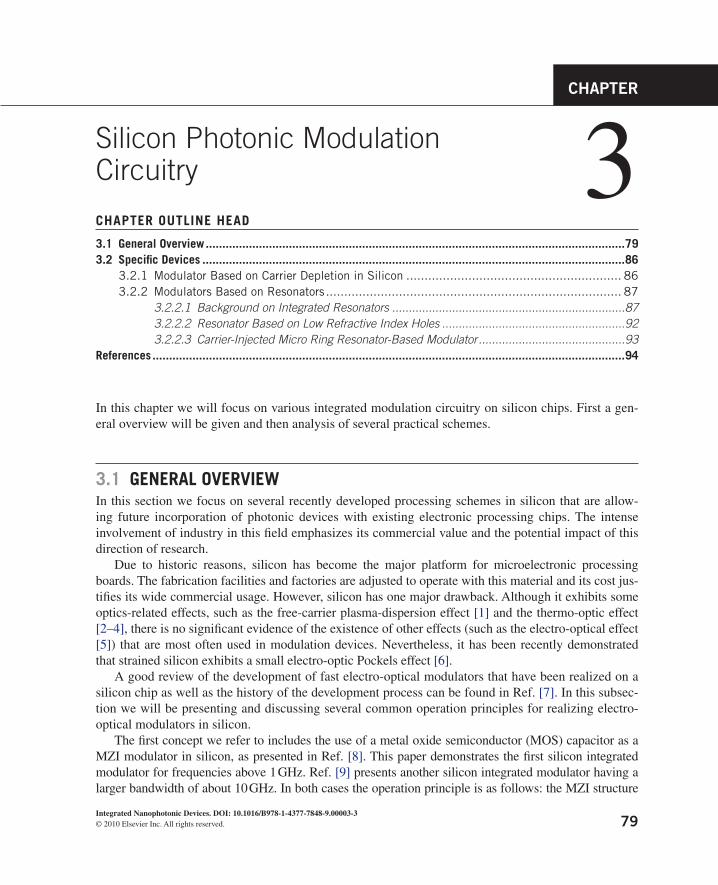
79Integrated Nanophotonic Devices. DOI:© 2010 Elsevier Inc. All rights reserved.
10.1016/B978-1-4377-7848-9.00003-32010
CHAPTER OUTLINE HEAD
3.1 General Overview ..............................................................................................................................793.2 Specific Devices ...............................................................................................................................86
3.2.1 Modulator Based on Carrier Depletion in Silicon ........................................................... 863.2.2 Modulators Based on Resonators ................................................................................. 87
3.2.2.1 Background on Integrated Resonators ......................................................................873.2.2.2 Resonator Based on Low Refractive Index Holes .......................................................923.2.2.3 Carrier-Injected Micro Ring Resonator-Based Modulator ............................................93
References ..............................................................................................................................................94
Silicon Photonic Modulation Circuitry 3
CHAPTER
In this chapter we will focus on various integrated modulation circuitry on silicon chips. First a gen-eral overview will be given and then analysis of several practical schemes.
3.1 GENERAL OvERvIEwIn this section we focus on several recently developed processing schemes in silicon that are allow-ing future incorporation of photonic devices with existing electronic processing chips. The intense involvement of industry in this field emphasizes its commercial value and the potential impact of this direction of research.
Due to historic reasons, silicon has become the major platform for microelectronic processing boards. The fabrication facilities and factories are adjusted to operate with this material and its cost jus-tifies its wide commercial usage. However, silicon has one major drawback. Although it exhibits some optics-related effects, such as the free-carrier plasma-dispersion effect [1] and the thermo-optic effect [2–4], there is no significant evidence of the existence of other effects (such as the electro-optical effect [5]) that are most often used in modulation devices. Nevertheless, it has been recently demonstrated that strained silicon exhibits a small electro-optic Pockels effect [6].
A good review of the development of fast electro-optical modulators that have been realized on a silicon chip as well as the history of the development process can be found in Ref. [7]. In this subsec-tion we will be presenting and discussing several common operation principles for realizing electro-optical modulators in silicon.
The first concept we refer to includes the use of a metal oxide semiconductor (MOS) capacitor as a MZI modulator in silicon, as presented in Ref. [8]. This paper demonstrates the first silicon integrated modulator for frequencies above 1 GHz. Ref. [9] presents another silicon integrated modulator having a larger bandwidth of about 10 GHz. In both cases the operation principle is as follows: the MZI structure
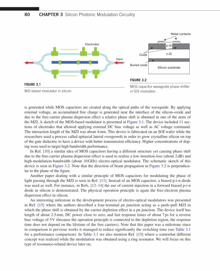
80 CHAPTER 3 Silicon Photonic Modulation Circuitry
is generated while MOS capacitors are created along the optical paths of the waveguide. By applying external voltage, an accumulated free charge is generated near the interface of the silicon–oxide and due to the free-carrier plasma dispersion effect a relative phase shift is obtained in one of the arms of the MZI. A sketch of the MOS-based modulator is presented in Figure 3.1. The device included 11 sec-tions of electrodes that allowed applying external DC bias voltage as well as AC voltage command. The interaction length of the MZI was about 4 mm. This device is fabricated on an SOI wafer while the researchers used a process called epitaxial lateral overgrowth in order to grow crystalline silicon on top of the gate dielectric to have a device with better transmission efficiency. Higher concentrations of dop-ing were used to target high bandwidth performance.
In Ref. [10] a similar idea of MOS capacitors having a different structure yet causing phase shift due to the free-carrier plasma dispersion effect is used to realize a low-insertion-loss (about 2 dB) and high-modulation-bandwidth (about 10 GHz) electro-optical modulator. The schematic sketch of this device is seen in Figure 3.2. Note that the direction of beam propagation in Figure 3.2 is perpendicu-lar to the plane of the figure.
Another paper dealing with a similar principle of MOS capacitors for modulating the phase of light passing through the MZI is seen in Ref. [11]. Instead of an MOS capacitor, a biased p-i-n diode was used as well. For instance, in Refs. [12–14] the use of current injection in a forward biased p-i-n diode in silicon is demonstrated. The physical operation principle is again the free-electron plasma dispersion effect in silicon.
An interesting milestone in the development process of electro-optical modulators was presented in Ref. [15] where the authors described a four-terminal pn junction acting as a push–pull MZI in which the phase shift is obtained by the carrier depletion effect in a pn junction. The device itself has length of about 2.5 mm, DC power close to zero, and fast response times of about 7 ps for a reverse bias voltage of 5 V (because the operation principle is connected to the depletion region, the response time does not depend on the lifetime of the free carriers). Note that this paper was a milestone since in comparison to previous works it managed to reduce significantly the switching time (see Table 3.1 for a performance comparison). In Table 3.1 we also mention Ref. [15] where a somewhat different concept was realized while the modulation was obtained using a ring resonator. We will focus on this type of resonance-related device later on.
Electrodes
Input
FIGURE 3.1
MZI-based modulator in silicon.
Silicon substrateBuried oxide
n-Si
p-Si
Oxide
Metal contacts
FIGURE 3.2
MOS capacitor waveguide phase shifter in SOI modulator.
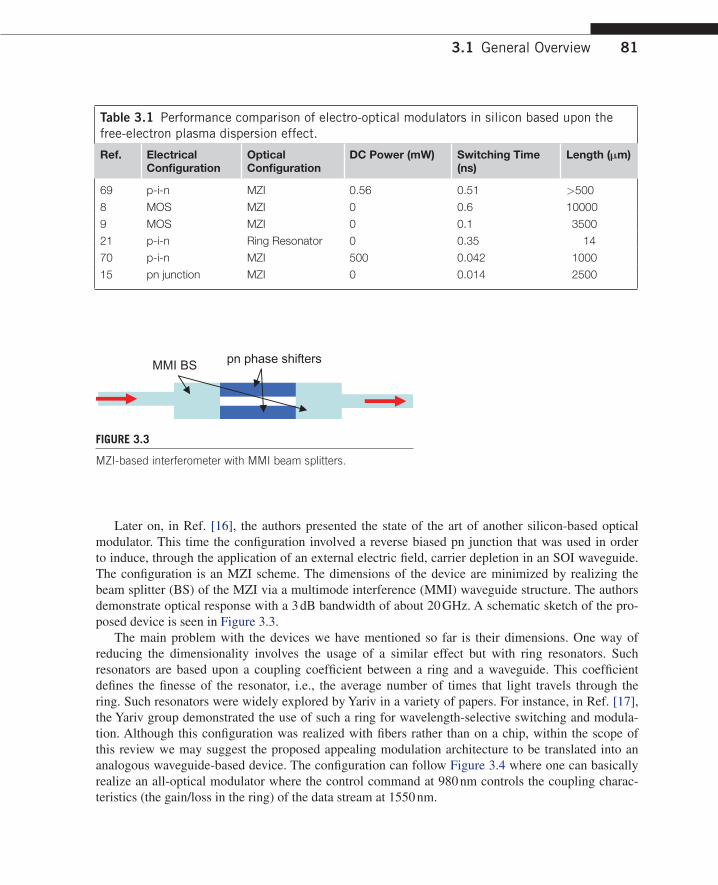
81
Later on, in Ref. [16], the authors presented the state of the art of another silicon-based optical modulator. This time the configuration involved a reverse biased pn junction that was used in order to induce, through the application of an external electric field, carrier depletion in an SOI waveguide. The configuration is an MZI scheme. The dimensions of the device are minimized by realizing the beam splitter (BS) of the MZI via a multimode interference (MMI) waveguide structure. The authors demonstrate optical response with a 3 dB bandwidth of about 20 GHz. A schematic sketch of the pro-posed device is seen in Figure 3.3.
The main problem with the devices we have mentioned so far is their dimensions. One way of reducing the dimensionality involves the usage of a similar effect but with ring resonators. Such resonators are based upon a coupling coefficient between a ring and a waveguide. This coefficient defines the finesse of the resonator, i.e., the average number of times that light travels through the ring. Such resonators were widely explored by Yariv in a variety of papers. For instance, in Ref. [17], the Yariv group demonstrated the use of such a ring for wavelength-selective switching and modula-tion. Although this configuration was realized with fibers rather than on a chip, within the scope of this review we may suggest the proposed appealing modulation architecture to be translated into an analogous waveguide-based device. The configuration can follow Figure 3.4 where one can basically realize an all-optical modulator where the control command at 980 nm controls the coupling charac-teristics (the gain/loss in the ring) of the data stream at 1550 nm.
Table 3.1 Performance comparison of electro-optical modulators in silicon based upon the free-electron plasma dispersion effect.
Ref. Electrical Configuration
Optical Configuration
DC Power (mW) Switching Time (ns)
Length (m)
69 p-i-n MZI 0.56 0.51 >500
8 MOS MZI 0 0.6 10000
9 MOS MZI 0 0.1 3500
21 p-i-n Ring Resonator 0 0.35 14
70 p-i-n MZI 500 0.042 1000
15 pn junction MZI 0 0.014 2500
pn phase shiftersMMI BS
FIGURE 3.3
MZI-based interferometer with MMI beam splitters.
3.1 General Overview

82 CHAPTER 3 Silicon Photonic Modulation Circuitry
We start our discussion on electro-optical modulators in silicon that also involve ring resonators by mentioning an interesting concept that uses the field effect [18]. There, the authors have demonstrated a silicon integrated electro-optical modulator based upon optical beam and free-carrier interaction. A ring-resonator-like structure with a highly confined optical mode is constructed while an accumula-tion layer is generated within the optical waveguiding ring by applying an external field (i.e., volt-age). Schematically the proposed device is described in Figure 3.5. The authors claim more than 7 dB of extinction ratio for an external voltage of only 2 V.
Later, in Ref. [19], the authors demonstrated a microscale ring structure that is realized on a sili-con chip. They tuned the extinction ratio by forward biasing either the microscale ring or the cross-coupled waveguide p-i-n diode while modulating the other.
In addition to the modulation capability, the authors also demonstrated OR logic switching by simultaneously applying the data stream both in the microscale ring as well as in the cross-coupled waveguide p-i-n diode. A schematic sketch of the device is depicted in Figure 3.6.
Another interesting scheme for a high-speed carrier injection modulator is described in Refs. [20,21] where a ring resonator is a silicon waveguide within a p-i-n diode. Modulation rates of 12 Gb/s and an extinction ratio of above 9 dB were reported. A schematic sketch of the described devices may be seen in Figure 3.7A while the structure of the p-i-n junction is seen in Figure 3.7B.
Following that, in Ref. [22], the authors used the same concept but in a cascaded ring structure in order to realize modulators for WDM optical interconnects. The idea here is that since each ring is a resonator it will modulate a certain wavelength, while the others will pass through without being modulated. Therefore, cascading several such ring modulators while each one is tuned to a different resonating wavelength can allow for independent modulation of every wavelength and thus it is suit-able for WDM interconnect applications.
Another related technology deals with the realization of a Fabry–Perot resonator [23] configura-tion rather than the ring configuration. In a Fabry–Perot resonator, two Bragg mirrors are positioned one in front of the other. The resonant frequency is inversely proportional to the distance between the mirrors since for those frequencies all the replications generated by the mirrors are added with phase which is a product of 2:
νm
mc
nd=
2 (3.1)
Er doped
Control: 980 nm pump
Data stream: 1550 nm
FIGURE 3.4
Usage of a ring resonator for the realization of an all-optical switch.
Input
Output
n-Sip-poly
Oxide
FIGURE 3.5
Field-effect modulator based upon a ring resonator.

83
where d is the distance between the mirrors, c is the light’s velocity in a vacuum, n is the refrac-tive index of the medium between the mirrors, and m is an integer index. Actually, a similar relation exists also for ring resonators where instead of 2d one should use the length of the ring. Leaving silicon briefly, a Fabry–Perot configuration can be used as an electrically controlled tunable filter if the medium between the mirrors is filled with an LC that is usually polarization-sensitive [23,24]. However, this sensitivity can be removed, as described by Abdulhalim [25].
Returning again to silicon, in Ref. [26], the authors present an electrically tunable Fabry–Perot resonator that is integrated on an SOI chip while the silicon light-guided core is bounded with Si/SiO2 Bragg reflectors generating finesse of 11.2. The length of the realized device was about 20 m long and a modulation depth of 53% was demonstrated for a power consumption of 20 mW. The effect that tuned the spectral response of the p-i-n resonator is the free-carrier generation (as in all the silicon-integrated devices that we have reviewed so far), which changed the refractive index of the core, i.e., of the medium between the Bragg reflectors. A schematic sketch of the setup is seen in Figure 3.8.
p+
n+
n+
n+
p+
p+
FIGURE 3.6
Electro-optical modulators and logic gates via a combined concept including ring resonators and a cross-coupled waveguide p-i-n diode.
(A) (B)
n+ p+
SiOxide Oxide
p+
n+
n+
Si waveguide
FIGURE 3.7
(A) Ring resonator is a silicon waveguide within a p-i-n diode. (B) The structure of the p-i-n junction.
p+
n+
Bragg reflectors
Input light
SOI wafer
Output light
FIGURE 3.8
Schematic sketch of an electro-optical modulator based upon a Fabry–Perot resonator.
3.1 General Overview

84 CHAPTER 3 Silicon Photonic Modulation Circuitry
Another interesting device involving Bragg reflectors and a Fabry–Perot resona-tor is presented in Ref. [27]. In this paper the authors have demonstrated a compact electro-optical modulator in which a p-i-n diode was used in order to inject free carriers that change the refractive index of a 1-D cavity. The cav-ity was bounded by Bragg reflectors that were generated by the insertion of low-refractive-index holes into the silicon waveguide. The entire device was 6 m in length with 5.87 dB of modulation depth at 250 Mbps. Figure 3.9 presents a schematic sketch of this device.
In addition to regular Bragg reflectors, radial Bragg reflectors, as mentioned in
Ref. [28], can also be used for the realization of compact electro-optical modulators. The topic of ring resonators was extended to ring resonators with radial Bragg reflectors. This interesting structure can in the future be implemented in SOI wafers and realize electro-optical or all-optical devices. The configuration is schematically described in Figure 3.9. The Bragg reflectors are generated in the radial axis and therefore the resonating modes that are developed in the resonator have angular symmetry.
So far we have discussed interesting approaches for realizing silicon-integrated electro-optical modulators. But in order to have a fully functional integrated circuit, other components need to be available as well. Another interesting aspect of silicon photonics is related to the attempts of gener-ating a laser and all-optical devices on a silicon chip. In both cases the physical operation principle resists to be the free-electron plasma dispersion effect and it is replaced by non-linear effects such as Raman scattering and TPA.
Intel researchers [29,30] have managed to construct light amplification and a laser in silicon. The concept is based upon using stimulated Raman scattering in order to generate a light source on a silicon chip that later on can be integrated with other optoelectronic and microelectronic devices fab-ricated in the same chip. The silicon Raman-based laser was generated using a low-loss optical sin-gle-mode waveguide containing a reverse biased p-i-n diode structure. The optical cavity was formed by coating one facet and leaving the second one uncoated. The coating was a multilayered coating that was designed to have high reflectivity for the pumping (around 1.55 m) as well as for the lasing Raman Stokes wavelength around 1.68 m.
Reference [31] is another example where a continuous silicon laser based upon the Raman effect is presented. The non-linear losses of silicon related to TPA and induced free-carrier absorption limited the silicon Raman lasing to pulsed operation mode. The reverse biased p-i-n diode embedded in the silicon waveguide reduced those losses and allowed for continuous operation. In Ref. [31] the authors used a ring resonator for realizing an all-optical modulator. In this concept free carriers were induced into the ring resonator by a TPA process. The free carriers changed the refractive index of the ring and therefore tuned its resonance wavelength. In this paper a modulation depth of above 90% was demonstrated with a wavelength shift of 0.36 nm and a relaxation time of about 0.5 ns. Note that the first observations of stimulated Raman scattering in a silicon waveguide (SOI) were reported in Refs. [32,33]. There the authors demonstrated the generation of amplification of Stokes signals at 1542.3 nm for pumping of
Sin+ p+
Cavity Bragg reflectors
SOI
FIGURE 3.9
Schematic sketch of an electro-optical modulator based upon Bragg reflectors.

85
1427 nm. The main problem is that the bandwidth of the optical gain is just over 1 nm. The next step was the demonstration of net gain over a bandwidth range of 28 nm through an optical process of four-wave mixing while having phase matching in properly designed SOI channel waveguides. In that paper, the authors also demonstrated wavelength conversion within the range of 1511–1591 nm with very high conversion efficiency of more than 5.2 dB. This work was later extended in Ref. [34] and recently in Ref. [35] where a realization of a broadband optical parameter gain on a silicon chip is presented.
Another interesting application of the TPA process can be energy harvesting. For instance, in Refs. [36,37] the authors present how an off-chip light source is used in a TPA photovoltaic effect in which the illuminating photons energy is lost to two-photon absorption, which is harvested into useful elec-trical power rather than being dissipated into heat. For example, in the first paper they show that a power of 1 mW is attainable in 1-cm-long device with a 150 × 150-nm mode effective area.
In Ref. [38], the authors demonstrate all-optical logic AND and NAND gates that are realized on an SOI wafer. The operation principle is based upon the TPA effect and therefore the device is capa-ble of operating while the data stream wavelength and the control wavelength are similar and both are in the range around 1550 nm (which is good for optical communication). The operation principle is as follows: a strong control signal generates free-electron carriers due to the TPA process. The free car-riers affect the information beam due to the silicon plasma dispersion effect. In that paper the authors report achieving an operation rate of 310 Mbps with an extension ratio of 10 dB while the ring resona-tor has a diameter of about 10 m and Q of 10 (Q is related to the finesse of the ring resonator).
Note that, except for the need to generate light sources and modulators on SOI chips, in order to have a fully integrated optical solution, photodetection is required as well. In Ref. [39] a monolithic approach for the integration of modulators and photodetectors on the same SOI wafer is discussed. The modulator is based upon the electro-absorption effect in GeSi, which is due to the Franz–Keldysh effect. The use of GeSi provides an efficient monolithic process for integrating the modulator and the photodetectors on the SOI platform. Other concepts for Ge-on-SOI and Ge-integrated photodetectors may be seen in Refs. [40–42].
Another direction that is connected to integrated photodetection but which can be used as a modu-lated light source is related to quantum dots [43]. A quantum dot is a semiconductor nanostructure (such as a nanocrystal) that confines the motion capability of conduction-band electrons and/or valence-band holes in all three spatial dimensions. Quantum dots were proven to be useful for optical memories [44], highly luminescent sources [45,46], LEDs [47,48], white light sources [49], photo-voltaic cells [50], photodetectors [51], and eventually recently as silicon-integrated detectors [52].
Except for the realization of a laser source, electro-optical and all-optical modulators, and logic gates in silicon, there are other derivatives of the effects reviewed in this paper. Devices such as opti-cally tunable slow light [53], four-wave mixing effects in SOI waveguides [54–56], all-optical delays [57], all-optical switches [58], optical signal regenerators [59], and optical sources for quantum infor-mation technology [60] were all demonstrated using four-wave mixing in silica fibers and can now be easily transferred to the SOI platform.
Note that in this paper we have mentioned non-linear optical approaches for the realization of all-optical logic gates. However, if low cascading capability is required, such devices can be realized in silicon with linear devices based upon the MMI concept [61].
As a final note to this section we would like to emphasize that the presented concepts for inte-grated silicon devices are to be used not only for local processing purposes but rather as applicable components of optical networks [62].
3.1 General Overview

86 CHAPTER 3 Silicon Photonic Modulation Circuitry
3.2 SPECIFIC DEvICESLet us now focus on several selected silicon photonic devices and understand their operation princi-ples with more details.
3.2.1 Modulator Based on Carrier Depletion in SiliconIn Ref. [16] the authors presented the realization of a high-speed silicon modulator based on carrier depletion in silicon waveguide. The basic phenomenon is related to the plasma dispersion effect men-tioned in the previous chapter of this book. The free carriers’ generation is related to depletion region of pn junctions. The device described in Ref. [16] is based on an MZI with a reverse-biased pn diode embedded in each of the two arms of the interferometer. The MMI coupler is used because it has a broader range of operating wavelengths and larger fabrication tolerance as compared to a directional coupler.
The fabrication process was designed to target the pn junction at approximately 0.4 m above the buried oxide to enable optimal modal overlap with the depletion region. As the n-doping concentration is much higher than the p-doping concentration, carrier depletion under reverse bias occurs mainly in the p-type doped region which results by improved phase modulation efficiency due to the hole density change providing larger refractive index change as compared to the electron density change.
Note that pn junction-based silicon modulator has a fast intrinsic response (the transverse response time is ∼7 ps). However, in order to obtain the high-frequency operation it is essential to overcome the issues associated with the relatively large pn junction capacitance and metal contact parasitics. To minimize the RC limitation of the frequency response of the modulator the authors of Ref. [16] real-ized traveling wave electrode based on coplanar waveguide structure. The RF traveling wave coplanar waveguide and modulator optical waveguide are carefully designed so that both electrical and optical signals co-propagate along the length of the phase shifter with similar speeds, while, at the same time, the RF attenuation is kept as small as possible.
For a reverse-biased pn junction, the depletion width depends on the bias voltage and doping con-centrations. For the asymmetrically doped pn junction as done in Ref. [16] the depletion width (WD) can be approximated following the formulations presented in the theoretical background chapter on semiconductors:
WV V
qNDr bi in
A
=+( )2 0e e
(3.2)
where e0 and er are the vacuum permittivity and the low-frequency relative permittivity of silicon, q is the electron charge, NA is the acceptor concentration, Vbi is the built-in voltage and Vin is the applied voltage. Changing the depletion width of a pn junction is equivalent to changing the free carrier den-sity. Thus, by changing the bias voltage, one can achieve refractive index modulation through the free carrier plasma dispersion effect.
Photonic modulators based upon the depletion region have small signal transient response which determines the feasibility of the device to be used for high-speed data modulation. The small signal response will be defined by the depletion or junction capacitance CJ [15]. Following the technical

87
background given in the chapter on semiconductors, the capacitance associated with the depletion region CJ is given by:
C Aq N N
N N VJs A D
A D B D
=+( ) ⋅ +( )e
2
where A is the area of the junction, q is the charge of an electron, eS is the permittivity of silicon, NA is the concentration of acceptors, ND is the concentration of donors, B is the potential difference at the junction and VD is the voltage applied to the junction.
3.2.2 Modulators Based on Resonators3.2.2.1 Background on Integrated ResonatorsDue to the fact that the electro-photonic interaction of light and matter in silicon has relatively small coefficients, in order to be able to realize photonic devices with reduced interaction length many sili-con photonic devices are based upon resonators, e.g. ring resonators. Micro-ring resonators are ver-satile wavelength-selective elements that can be used to synthesize a wide class of filter functions [63,64]. Many theoretical designs have been proposed to optimize the filter response and other prop-erties using various coupled resonator arrays [65,66], while compact resonators have been demon-strated in a number of semiconductor materials [67] and glass waveguides [68]. The finesse of the resonator is related to the number of times that the light travels through the resonator (e.g. a ring) and thus if high finesse is realized, more compact devices can be used.
The operation principle of ring resonators is similar to the basic concept of the Fabry–Perot reso-nator. Let us assume the schematic sketch shown in Figure 3.10.
3.2 Specific Devices
n′
n′
n L
C
θ
B
Ai
A
A1 A2
B2B1
2θ
θ′
FIGURE 3.10
Schematic sketch of rays reflected between two mirrors separated by a distance L.

88 CHAPTER 3 Silicon Photonic Modulation Circuitry
The refractive index of the material between two mirrors is denoted by n and the refractive index of the materials outside the mirrors by n′. We assume that an incident ray with an amplitude of Ai is arriv-ing at the first mirror surface at an angle of ′. The amplitudes of the back-reflected beams are B1, B2 etc., while the subscript indicates the order of reflection. The amplitudes of the transmitted beams are denoted by A1, A2 etc., while again the subscript indicates the order of transmission. We assume that the transmission coefficient for the electrical field when going from material n′ towards material n is denoted by t and the transmission coefficient for light going in the opposite direction is t′. The reflec-tive coefficients for the field are denoted as and ″ for beam that is back-reflected from material with refraction index of n or n′ respectively.
Let us start by computing the length of the paths CB and BA which are responsible for the phase optical path difference generated between any two adjacent transmitted beams. The sum of the paths equals:
CB BA L+ = 2 cos (3.3)
Thus the optical path difference will be:
ν
= +( ) = =2 4 4n
CB BAnL n
cV V
cos cos
(3.4)
where V is the wavelength in vacuum and c is the speed of light in vacuum. The coefficients of the reflected field are:
B AB tt A i
B tt A i i
B B
i
i
i
n n
1
2
32
==
= ( )
=
′ ′
′ ′ ′
exp( )
exp( ) exp( )
−− ( )12′ exp( )i
(3.5)
Using the geometrical series expression yields:
B B A tti
itot n
ni= = +
( )− ( )
∑
′ ′′
exp
exp
1 2
(3.6)
The expressions for the amplitudes of the transmitted field yield:
A A tt i
A A tt i i
A A tt i
i
i
i
1
22
3
=
= ( )=
′ ′
′ ′ ′
′
exp( )
exp( ) exp( )
exp(
′′ ′
′
) exp( )
exp( )
2 2
12
i
A A in n
( )
= ( )−
(3.7)

89
and the final results of the summation equal:
A A A tti
itot n
ni= =
( )− ( )∑ ′ ′
′
′
exp
exp
1 2
(3.8)
where
′ =2 n L
V cos (3.9)
Following the Stokes principle we have:
′′= −= −tt 1 2
(3.10)
Thus, one may obtain that the reflection or transmitted ratios equal:
A
A
i
i
B
A
i
i
tot
i
tot
i
= −( ) ( )− ( )
=− ( )−
11
1
1
22
2
exp
exp
exp
exp
′
(( )
(3.11)
Those relations are for the electric field. For intensities one obtains:
I
I
A
A
R
R R
I
I
B
A
t
i
tot
i
r
i
tot
i
= =−( )
−( ) + ( )
=
| |
| | sin /
| |
| |
2
2
2
2 2
2
1
1 4 2
22
2
2 2
4 2
1 4 2=
( )−( ) + ( )
R
R R
sin /
sin /
(3.12)
where R is the reflection coefficient for the intensity:
R = | | 2 (3.13)
One may clearly see the conservation of energy, since:
I
I
I
Ir
i
t
i
+ = 1
(3.14)
Optical frequencies of maximal transmission are obtained when the expression for It/Ii is maxi-mized, i.e. for:
ν
m mc
nL=
2 cos (3.15)
3.2 Specific Devices

90 CHAPTER 3 Silicon Photonic Modulation Circuitry
where m is an integer number. The distance between two transmission peaks, also called the free spectral range (FSR), is equal to:
ν ν ν
= − =+m m
c
nL1 2 cos (3.16)
and in order to convert this equation to wavelength units, we use the well-known relation of:
νm m c= , (3.17)
to obtain:
νν
ν= =
c
c2
2
(3.18)
yielding:
=2
2nL cos (3.19)
From Eq. 3.16 one may extract the frequencies of the peaks:
ν νm m= (3.20)
Defining the criteria of half width half maximum (HWHM) as the width of each transmission peak:
I
It
i=2
(3.21)
yields the following:
4 2 12
1 22
R Rsin //( ) = −( ) (3.22)
which results in:
HWHM = − =
− 1 2 2
1/ m
R
R (3.23)
Thus, the width of the peak is equal to:
ν
1 2 1 24 4
2 2/ /cos cos= ⋅ = ⋅ −( )c
nL
c
nLm
(3.24)
or:
ν
ν1 2 2
1 1/ cos= ⋅
−= ⋅
−c
nL
R
R
R
R (3.25)

91
Following that, the finesse of the resonator is defined as:
ℑ = =
−νν
1 2 1/
R
R (3.26)
The main advantage of using a ring resonator is the good match it proposes for integrated cir-cuits and waveguides. The theory of ring resona-tors is similar to the previously developed insights on Fabry–Perot. However, some parameters are expressed differently. Ring resonators sometimes have four terminals coupled together through two couplers. The coupling efficiency is determined according to the proximity between the waveguides and the ring structure in the center of the resonator (schematic sketch is seen in Fig. 3.11).
If a wavelength m satisfies the resonant condition of
n D meff m =
(3.27)
and is input through terminal 1, the coupling of the wave with that wavelength will be enhanced and all others will be suppressed. As a result, only this wavelength will be dropped from terminal 4, while the rest of the wavelengths will pass through and output from terminal 2. In the last equation neff is the effective refractive index of the bending waveguide, D is the diameter of the ring and m is an integer. If observing again Eq. 3.15 and using the relation connecting the optical wavelength and the optical frequency (Eq. 3.17) one obtains that for Fabry–Perot the resonance condition is:
n L meff m2 cos =
(3.28)
and thus by choosing D∼2Lcos both equations will coincide, simply because D represents the cir-cumference of the ring. The FSR is one of the key specifications of the ring resonator. It is defined as:
FSR =+( )
m
eff cn D L
2
(3.29)
where Lc is the length of the coupler. If comparing this with Eq. 3.19 one may see that for D + Lc∼2Lcos both equations coincide.
Because the FSR is inversely proportional to the size of the ring resonator, the ring must be small in order to achieve a high FSR. The finesse of the ring resonator is defined in the same way as in Fabry–Perot (Eq. 3.26) but the “reflectivity” R is defined as:
R = − −exp( )( ) 1 (3.30)
where is the total amplitude attenuation coefficient for each round trip, and is the normalized cou-pling coefficient of the coupler.
3.2 Specific Devices
FIGURE 3.11
Schematic sketch of ring resonator.
Terminal 4 Terminal 3
Terminal 1 Terminal 2
Coupler 2
Coupler 1
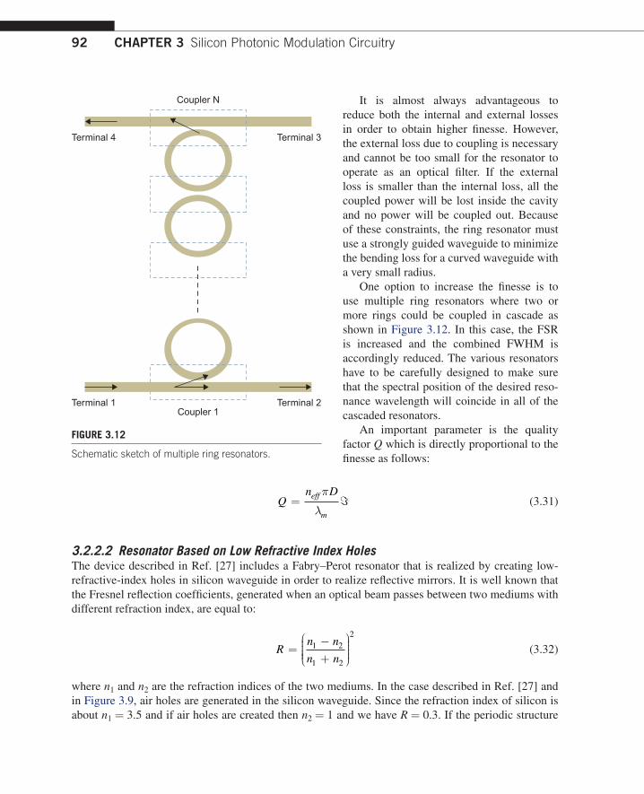
92 CHAPTER 3 Silicon Photonic Modulation Circuitry
It is almost always advantageous to reduce both the internal and external losses in order to obtain higher finesse. However, the external loss due to coupling is necessary and cannot be too small for the resonator to operate as an optical filter. If the external loss is smaller than the internal loss, all the coupled power will be lost inside the cavity and no power will be coupled out. Because of these constraints, the ring resonator must use a strongly guided waveguide to minimize the bending loss for a curved waveguide with a very small radius.
One option to increase the finesse is to use multiple ring resonators where two or more rings could be coupled in cascade as shown in Figure 3.12. In this case, the FSR is increased and the combined FWHM is accordingly reduced. The various resonators have to be carefully designed to make sure that the spectral position of the desired reso-nance wavelength will coincide in all of the cascaded resonators.
An important parameter is the quality factor Q which is directly proportional to the finesse as follows:
Q
n Deff
m
= ℑ
(3.31)
3.2.2.2 Resonator Based on Low Refractive Index HolesThe device described in Ref. [27] includes a Fabry–Perot resonator that is realized by creating low-refractive-index holes in silicon waveguide in order to realize reflective mirrors. It is well known that the Fresnel reflection coefficients, generated when an optical beam passes between two mediums with different refraction index, are equal to:
Rn n
n n=
−+
1 2
1 2
2
(3.32)
where n1 and n2 are the refraction indices of the two mediums. In the case described in Ref. [27] and in Figure 3.9, air holes are generated in the silicon waveguide. Since the refraction index of silicon is about n1 = 3.5 and if air holes are created then n2 = 1 and we have R = 0.3. If the periodic structure
Terminal 4 Terminal 3
Coupler N
Terminal 1 Terminal 2Coupler 1
FIGURE 3.12
Schematic sketch of multiple ring resonators.
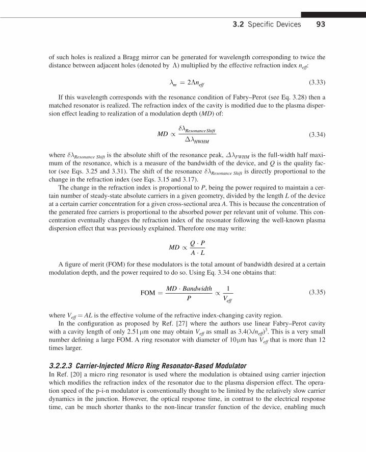
93
of such holes is realized a Bragg mirror can be generated for wavelength corresponding to twice the distance between adjacent holes (denoted by Λ) multiplied by the effective refraction index neff:
m effn= 2Λ
(3.33)
If this wavelength corresponds with the resonance condition of Fabry–Perot (see Eq. 3.28) then a matched resonator is realized. The refraction index of the cavity is modified due to the plasma disper-sion effect leading to realization of a modulation depth (MD) of:
MD
ResonanceShift
HWHM
∝
(3.34)
where Resonance Shift is the absolute shift of the resonance peak, FWHM is the full-width half maxi-mum of the resonance, which is a measure of the bandwidth of the device, and Q is the quality fac-tor (see Eqs. 3.25 and 3.31). The shift of the resonance Resonance Shift is directly proportional to the change in the refraction index (see Eqs. 3.15 and 3.17).
The change in the refraction index is proportional to P, being the power required to maintain a cer-tain number of steady-state absolute carriers in a given geometry, divided by the length L of the device at a certain carrier concentration for a given cross-sectional area A. This is because the concentration of the generated free carriers is proportional to the absorbed power per relevant unit of volume. This con-centration eventually changes the refraction index of the resonator following the well-known plasma dispersion effect that was previously explained. Therefore one may write:
MDQ P
A L∝
⋅⋅
A figure of merit (FOM) for these modulators is the total amount of bandwidth desired at a certain modulation depth, and the power required to do so. Using Eq. 3.34 one obtains that:
FOM =⋅
∝MD Bandwidth
P Veff
1
(3.35)
where Veff = AL is the effective volume of the refractive index-changing cavity region.In the configuration as proposed by Ref. [27] where the authors use linear Fabry–Perot cavity
with a cavity length of only 2.51 m one may obtain Veff as small as 3.4(/neff)3. This is a very small
number defining a large FOM. A ring resonator with diameter of 10 m has Veff that is more than 12 times larger.
3.2.2.3 Carrier-Injected Micro Ring Resonator-Based ModulatorIn Ref. [20] a micro ring resonator is used where the modulation is obtained using carrier injection which modifies the refraction index of the resonator due to the plasma dispersion effect. The opera-tion speed of the p-i-n modulator is conventionally thought to be limited by the relatively slow carrier dynamics in the junction. However, the optical response time, in contrast to the electrical response time, can be much shorter thanks to the non-linear transfer function of the device, enabling much
3.2 Specific Devices
94 CHAPTER 3 Silicon Photonic Modulation Circuitry
faster modulation. The non-linear relationship between the optical transmission T at wavelength of 0 and the total charge qtot in the junction is given by [20]:
T
q Q
qn V
q Q
qn V
tot
g eff
tot
g eff
=
+
2
12
0
2
0
2
(3.36)
where q is the charge of an electron, ng = 4.3 is the group index of the ring, Veff = 4.5 × 10⁻¹²[cm3] is the volume of the junction, 0 = 0.8 is the mode confinement factor, ≈ 4.3 × 10⁻²¹[cm3] is the ratio between the change of refractive index of silicon and the electron-hole-pair density N when N ≈ 1017[cm−3] and Q ≈ 20 000 is the quality factor of the ring resonator.
For simplicity, we assume that the ring resonator is critically coupled to the waveguide, so that the optical transmission is zero at 0. When the p-i-n diode is forward biased, the electron and hole densities in the intrinsic region are equal, which means that the total charge carried by electrons and holes satisfies −qe = qh = qtot. Under dynamic driving voltage, the charge qtot in the junction follows the first-order dif-ferential equation involving the serial resistance of the diode and the average carrier recombination lifetime in the device (denoted as ). The rise time of the optical transmission is much shorter than the rise time of the charge dynamics, which is determined by the carrier dynamics with positive bias voltage.
The rise time of the charge injection, defined as the time needed for qtot to reach 0.9 of the steady-state charge, is proportional to . On the other hand one can see that the optical transmission quickly saturates to about 100% as the charge qtot increases. Specifically, the transmission T > 90% as long as we have charge of q qn V qtot g eff tot> 3 2 0 . Therefore, the optical rise time is only determined by the time needed to inject this amount of charge into the junction, which can be much shorter than the rise time of charge injection, if this charge is smaller than the steady-state charge.
Note that the photon lifetime of a ring resonator at 0 resonance can be obtained from the quality factor as:
cav
Q
c= 0
2 (3.37)
where c is the speed of light. This lifetime can be equal to 9.1 ps in case of a ring resonator with Q factor of about 10 000 (and a diameter of 10 m as presented in Ref. [38]) and at wavelength around 1550 nm. This lifetime gives the fundamental limit to the operation speed of the device which once again can be a very high one and to match the constantly increasing requirements in the field of optics communication.
References [1] R.A. Soref, B.R. Bennett, Electro-optical effects in silicon, IEEE J. Quantum Electron. 23 (1987) 123–129. [2] S.T. Feng, E.A. Irene, Thermo-optical switching in Si based etalons, J. Appl. Phys. 72 (1992) 3897–3903. [3] R.L. Espinola, M.C. Tsai, J.T. Yardley, R.M. Osgood, Fast and low-power thermo-optic switch on thin
silicon-on-insulator, IEEE Photon. Technol. Lett. 15 (2003) 1366–1368.

95
[4] L. Pavesi, D.J. Lockwood, Silicon Photonics, in vol. 94, Topics in Applied Physics Series, Springer, New York, 2004.
[5] G.T. Reed, A.P. Knights, Silicon Photonics: An Introduction, Wiley, Chichester, UK, 2004. [6] R.S. Jacobsen, K. Andersen, P.I. Borel, J. Fage-Pedersen, L.H. Frandsen, O. Hansen, et al., Strained silicon
as a new electro-optics material, Nature 441 (2006) 199–202. [7] G.T. Reed, The optical age of silicon, Nature 427 (2004) 595–596. [8] A. Liu, R. Jones, L. Liao, D. Samara-Rubio, D. Rubin, O. Cohen, et al., A high speed silicon optical modu-
lator based on a metal-oxide-semiconductor capacitor, Nature 427 (2004) 615–618. [9] L. Liao, D. Samara-Rubio, M. Morse, A. Liu, D. Hodge, D. Rubin, et al., High speed silicon Mach–Zehnder
modulator, Opt. Exp. 13 (2005) 3129–3135. [10] A. Liu, D. Samara-Rubio, L. Liao, M. Paniccia, Scaling the modulation bandwidth and phase efficiency of
a silicon optical modulator, IEEE J. Sel. Top. Quantum Electron. 11 (2005) 367–372. [11] D. Samar-Rubio, U.D. Keil, L. Liao, T. Franck, A. Liu, D.W. Hodge, et al., Customized drive electronics to
extended silicon optical modulators to 4Gb/s, J. Lightwave Technol. 23 (2005) 4305–4314. [12] G.V. Treyz, P.G. May, J.M. Halbout, Silicon Mach–Zehnder waveguide interferometers based on the plasma
effect, Appl. Phys. Lett. 59 (1991) 771–773. [13] C.K. Tang, G.T. Ree, Highly efficient optical phase modulator in SOI waveguides, Electron. Lett. 31 (1995)
451–452. [14] P. Dainesi, A. Kung, M. Chabloz, A. Lagos, P. Fluckiger, A. Ionescu, et al., CMOS compatible fully inte-
grated Mach–Zehnder interferometer in SOI technology, IEEE Photon. Technol. Lett. 12 (2000) 660–662. [15] F. Gardes, G. Reed, N. Emerson, C. Png, A sub-micron depletion-type photonic modulator in silicon-
on-insulator, Opt. Exp. 13 (2005) 8845–8854. [16] A. Liu, L. Liao, D. Rubin, H. Nguyen, B. Ciftcioglu, Y. Chetrit, et al., High-speed optical modulation based
on carrier depletion in a silicon waveguide, Opt. Exp. 15 (2) (2007) 660–668. [17] J.M. Choi, R.K. Lee, A. Yariv, Control of critical coupling in a ring resonator fiber configuration: appli-
cation to wavelength-selective switching, modulation, amplification, and oscillation, Opt. Lett. 26 (2001) 1236–1238.
[18] R.D. Kekatpure, M.L. Brongersma, R.S. Shenoy, Design of a silicon-based field-effect electro-optic modulator with enhanced light-charge interaction, Opt. Lett. 30 (2005) 2149–2151.
[19] C. Li, L. Zhou, A.W. Poon, Silicon micro-ring carrier-injection-based modulators/switches with tun-able extinction ratios and OR-logic switching by using waveguide cross-coupling, Opt. Exp. 15 (2007) 5069–5076.
[20] Q. Xu, S. Manipatruni, B. Schmidt, J. Shakya, M. Lipson, 12.5 Gbit/s carrier-injection-based silicon micro-ring silicon modulators, Opt. Exp. 15 (2007) 430–436.
[21] Q. Xu, B. Schmidt, S. Pradhan, M. Lipson, Micrometre-scale silicon electro-optic modulator, Nature 435 (2005) 325–327.
[22] Q. Xu, B. Schmidt, J. Shakya, M. Lipson, Cascaded silicon micro-ring modulators for WDM optical inter-connection, Opt. Exp. 14 (2006) 9431–9435.
[23] G. Shabtay, E. Eidinger, Z. Zalevsky, D. Mendlovic, E. Marom, Tunable birefringent filters – optimal itera-tive design, Opt. Exp. 10 (2002) 1534–1541.
[24] Z. Zalevsky, F. Luan, W.J. Wadsworth, S.L. Saval, T.A. Birks, Liquid crystal based in-fiber tunable spectral structures, Opt. Eng. 45 (2006) 335005.
[25] I. Abdulhalim, Unique optical properties of anisotropic helical structures in a Fabry–Perot cavity, Opt. Lett. 31 (2006) 3019–3021.
[26] C.A. Barrios, V.R. Almeida, R.R. Panepucci, B.S. Schmidt, M. Lipson, Compact silicon tunable Fabry–Perot resonator with low power consumption, IEEE Photon. Technol. Lett. 16 (2004) 506–508.
[27] B. Schmidt, Q. Xu, J. Shakya, S. Manipatruni, M. Lipson, Compact electro-optic modulator on silicon- on-insulator substrates using cavities with ultra-small modal volumes, Opt. Exp. 15 (2007) 3140–3148.
References
96 CHAPTER 3 Silicon Photonic Modulation Circuitry
[28] J. Scheuer, A. Yariv, Two-dimensional optical ring resonators based on radial Bragg resonance, Opt. Lett. 28 (2003) 1528–1530.
[29] A. Liu, H. Rong, R. Jones, O. Cohen, D. Hak, M. Paniccia, Optical amplification and lasing by stimulated Raman scattering in silicon waveguides, J. Lightwave Technol. 24 (2006) 1440–1455.
[30] H. Rong, A. Liu, R. Jones, O. Cohen, D. Hak, R. Nicolaescu, et al., An all-silicon Raman laser, Nature 433 (2005) 292–294.
[31] H. Rong, R. Jones, A. Liu, O. Cohen, D. Hak, A. Fang, et al., A continuous wave Raman silicon laser, Nature 433 (2005) 725–728.
[32] R. Claps, D. Dimitropoulos, V. Raghunathan, Y. Han, B. Jalali, Observation of stimulated Raman amplifica-tion in silicon waveguides, Opt. Exp. 11 (2003) 1731–1739.
[33] R. Claps, V. Raghunathan, D. Dimitropoulos, B. Jalali, Anti-Stokes Raman conversion in silicon wave-guides, Opt. Exp. 11 (2003) 2862–2872.
[34] O. Boyraz, B. Jalali, Demonstration of a silicon Raman laser, Opt. Exp. 12 (2004) 5269–5273. [35] M.A. Foster, A.C. Turner, J.E. Sharping, B.S. Schmidt, M. Lipson, A.L. Gaeta, Broad-band optical paramet-
ric gain on a silicon photonic chip, Nature 441 (2006) 960–962. [36] S. Fathpour, B. Jalali, Energy harvesting in silicon optical modulators, Opt. Exp. 14 (2006) 10795–10799. [37] K.K. Tsia, S. Fathpour, B. Jalali, Energy harvesting in silicon wavelength converters, Opt. Exp. 14 (2006)
12327–12333. [38] Q. Xu, M. Lipson, All-optical logic based on silicon micro-ring resonators, Opt. Exp. 15 (2007) 924–929. [39] J. Liu, D. Pan, S. Jongthammanurak, K. Wada, L.C. Kimerling, J. Michel, Design of monolithically inte-
grated GeSi electro-absorption modulators and photodetectors on a SOI platform, Opt. Exp. 15 (2007) 623–628.
[40] O.I. Dosunmu, D.D. Cannon, M.K. Emsley, L.C. Kimerling, M.S. Unlu, High-speed resonant cavity enhanced Ge photodetectors on reflecting Si substrates for 1550-nm operation, IEEE Photon. Technol. Lett. 17 (2005) 175–177.
[41] S.J. Koester, G. Dehlinger, J.D. Schaub, J.O. Chu, Q.C. Ouyang, A. Grill. Germanium-on-insulator photo-detectors. In: 2nd IEEE International Conference Group IV Photonics (2005) 171–173.
[42] M. Oehme, J. Werner, E. Kasper, M. Jutzi, M. Berroth, High bandwidth Ge p-i-n photodetector integrated on Si, Appl. Phys. Lett. 89 (2006) 071117.
[43] P. Bhattacharya, J. Sabarinathan, J. Topolaposancik, S. Chakravarty, P.-C. Yu, W. Zhou, Quantum dot photonic crystal light sources, Proc. IEEE 93 (2005) 1825–1838.
[44] M.B. Fischbein, M. Drndic, CdSe nanocrystal quantum-dot memory, Appl. Phys. Lett. 86 (2005) 193106. [45] M.A Hines, P. Guyot-Sionnest, Synthesis and characterization of strongly luminescent ZnS-capped CdSe
nanocrystals, J. Phys. Chem. 100 (1996) 468–471. [46] B.O. Dabbousi, J. Rodriguez-Viejo, F.V. Mikulec, J.R. Heine, H. Mattoussi, R. Ober, et al., (CdSe)ZnS
core-shell quantum dots: synthesis and characterization of a size series of highly luminescent nanocrystal-lites, J. Phys. Chem. B 101 (1997) 9463–9475.
[47] S. Coe, W.-K. Woo, M. Bawendi, V. Bulovic, Electroluminescence from single monolayers of nanocrystals in molecular organic devices, Nature 420 (2002) 800–803.
[48] S. Chaudhary, M. Ozkan, W.C.W. Chan, Trilayer hybrid polymer-quantum dot light-emitting diodes, Appl. Phys. Lett. 84 (2004) 2925–2927.
[49] S. Nizamoglu, T. Ozel, E. Sari, H.V. Demir, White light generation using CdSe/ZnS core-shell nanocrystals hybridized with InGaN/GaN light emitting diodes, Nanotech. 18 (2007) 065709.
[50] J. Liu, T. Tanaka, K. Sivula, A.P. Alivisatos, J.M.J. Fréchet, Employing end-functional polythiophene to control the morphology of nanocrystal–polymer composites in hybrid solar cells, J. Am. Chem. Soc. 126 (2004) 6550–6551.
[51] D. Qi, M.B. Fischbein, M. Drndic, S. Selmic, Efficient polymer–nanocrystal quantum-dot photodetectors, Appl. Phys. Lett. 86 (2005) 093103.
97
[52] E. Mutlugun, I.M. Soganci, H.V. Demir, Nanocrystal hybridized scintillators for enhanced detection and imaging on Si platforms in UV, Opt. Exp. 15 (2007) 1128–1134.
[53] Y. Okawachi, M. Foster, J. Sharping, A. Gaeta, Q. Xu, M. Lipson, All-optical slow-light on a photonic chip, Opt. Exp. 14 (2006) 2317–2322.
[54] H. Fukuda, K. Yamada, T. Shoji, M. Takahashi, T. Tsuchizawa, T. Watanabe, et al., Four-wave mixing in silicon wire waveguides, Opt. Exp. 13 (2005) 4629–4637.
[55] R. Espinola, J. Dadap, R. Osgood Jr., S. McNab, Y. Vlasov, C-band wavelength conversion in silicon pho-tonic wire waveguides, Opt. Exp. 13 (2005) 4341–4349.
[56] H. Rong, Y.-H. Kuo, A. Liu, M. Paniccia, O. Cohen, High efficiency wavelength conversion of 10 Gb/s data in silicon waveguides, Opt. Exp. 14 (2006) 1182–1188.
[57] J. Sharping, Y. Okawachi, J. van Howe, C. Xu, Y. Wang, A. Willner, et al., All-optical, wavelength and bandwidth preserving, pulse delay based on parametric wavelength conversion and dispersion, Opt. Exp. 13 (2005) 7872–7877.
[58] Q. Lin, R. Jiang, C.F. Marki, C.J. McKinstrie, R. Jopson, J. Ford, et al., 40 GB/s optical switching and wavelength multicasting in a two-pump parametric device, IEEE Photon. Technol. Lett. 17 (2005) 2376–2378.
[59] E. Ciaramella, S. Trillo, All-optical reshaping via four-wave mixing in optical fibers, IEEE Photon. Technol. Lett. 12 (2000) 849–851.
[60] X. Li, P.L. Voss, J.E. Sharping, P. Kumar, Optical fiber source of polarization entangled photons in the 1550 nm telecom band, Phys. Rev. Lett. 94 (2005) 053601.
[61] Z. Zalevsky, A. Rudnitsky, M. Nathan, Nano photonic and ultra fast all-optical processing modules, Opt. Exp. 13 (2005) 10272–10284.
[62] A. Barkai, Y. Chetrit, O. Cohen, R. Cohen, N. Elek, E. Ginsburg, et al., Integrated silicon photonics for opti-cal networks, J. Opt. Net. 6 (1) (2007) 25–47.
[63] M.K. Chin, S.T. Ho, Design and modeling of waveguide-coupled single-mode microring resonators, J. Lightwave Technol. 15 (1998) 1433–1446.
[64] B.E. Little, S.T. Chu, H.A. Haus, J. Foresi, J.-P Laine, Microring resonator channel dropping filters, J. Lightwave Technol. 15 (1997) 998–1005.
[65] G. Griffel, Synthesis of optical filters using ring resonator arrays, IEEE Photon. Technol. Lett. 12 (2000) 810–812.
[66] B.E. Little, S.T. Chu, W. Pan, Y. Kokubun, Microring resonator arrays for VLSI photonics, IEEE Photon. Technol. Lett. 12 (2000) 320–322.
[67] B.E. Little, J. Foresi, H.A. Haus, E.P. Ippen, W. Greene, S.T. Chu, Ultracompact Si/SiO2 micro-ring resona-tor channel dropping filter, IEEE Photon. Technol. Lett. 10 (1998) 549–551.
[68] T. Kominato, Y. Ohmori, N. Takato, H. Okazaki, M. Yasu, Ring resonators composed of GeO2-doped silica waveguides, IEEE J. Lightwave Tech. 10 (1992) 1781–1788.
[69] C.E. Png, G.T. Reed, R.M. Atta, G.J. Ensell, A.G.R. Evans, Development of small silicon modulators in silicon-on-insulator (SOI), Proc. SPIE 4997 (2003) 190–197 In: Photonics Packaging and Integration III, R. A. Heyler, D. J. Robbins, and G. E. Jabbour, (Eds).
[70] F. Gan, F.X. Kartner, High-speed silicon electrooptic modulator design, IEEE Photon. Technol. Lett. 17 (2005) 1007–1009.
References

99Integrated Nanophotonic Devices. DOI:© 2010 Elsevier Inc. All rights reserved.
10.1016/B978-1-4377-7848-9.00004-52010
CHAPTER OUTLINE HEAD
4.1 Methods for Image Formation...........................................................................................................1004.1.1 ElectronBeamDirectWriteLithography..................................................................... 1004.1.2 AtomicForceMicroscopicNanolithography................................................................ 1014.1.3 OpticalMask-LessLithography.................................................................................. 1024.1.4 CopyingExpositionMethods..................................................................................... 1034.1.5 ExtremeUltravioletLithography(EUV)....................................................................... 104
4.2 Methods to Pattern Surfaces ............................................................................................................1044.2.1 ChemicalEtching.................................................................................................... 1044.2.2 DeepReactive-IonEtching(DRIE)............................................................................. 1044.2.3 NanoimprintLithography.......................................................................................... 1054.2.4 Magneto-Lithography(ML)........................................................................................ 1064.2.5 LIGAProcess........................................................................................................... 1064.2.6 DepositionwithLift-Off............................................................................................ 1074.2.7 FocusedIonBeam(FIB)........................................................................................... 108
4.3 Applications of Nanophotonics and Nanotechnologies.......................................................................1094.3.1 Biochips................................................................................................................. 1094.3.2 ImplantableMedicalDevices.................................................................................... 1094.3.3 ArtificialOrgans....................................................................................................... 1094.3.4 MolecularMotors..................................................................................................... 1104.3.5 MolecularElectronics............................................................................................... 1104.3.6 Biosensors.............................................................................................................. 1104.3.7 Nanosensors............................................................................................................ 1104.3.8 SolarCells.............................................................................................................. 111
References ............................................................................................................................................111
Fabrication Aspects of Integrated Devices 4
CHAPTER
Nanofabrication technologies are applied for the manufacturing of nanoscale devices applicable to fields of research such as microelectronics or nanophotonics. Usually the fabricated devices are made out of semiconductor materials, dielectrics, oxides and metals. Most of the manufacturing processes of nanoscale devices consist of two basic stages:
l Formation of an image on a surface of a materiall Processing and patterning the surface.
In this chapter we intend to review some of the fabrication techniques to be used for realization of the integrated nanophotonic devices that are overviewed in this book.
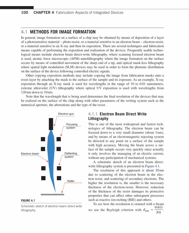
100 CHAPTER 4 Fabrication Aspects of Integrated Devices
4.1 METHODS FOR IMAgE FORMATIONIn general, image formation on a surface of a chip may be obtained by means of deposition of a layer of a photosensitive material – photo-resist, or a material sensitive to an electron beam – electron-resist, or a material sensitive to an X-ray and then its exposition. There are several techniques and fabrication means capable of performing the exposition and realization of the devices. Frequently usable techno-logical means include electron beam direct-write lithography, where scanning focused electron beam is used, atomic force microscopic (AFM) nanolithography where the image formation on the surface occurs by means of controlled movement of the sharp end of a tip, and optical mask-less lithography where spatial light modulation (SLM) devices may be used in order to form the photonic distribution on the surface of the device following controlled electric signals.
Other copying exposition methods may include copying the image from fabrication masks onto a resist layer by attaching the mask to the surface of the sample and its exposure. As an example, X-ray exposition through an X-ray mask is used for wavelengths in the range of 10 to 0.01 nanometers, extreme ultraviolet (UV) lithography where optical UV exposition is used with wavelengths from 120 nm down to 10 nm.
Note that the wavelength that is being used determines the final resolution of the devices that may be realized on the surface of the chip along with other parameters of the writing system such as the numerical aperture, the aberrations and the type of the resist.
4.1.1 Electron Beam Direct Write LithographyThis is one of the most widespread and fastest tech-nologies of lithography. The electron beam can be focused down to a very small diameter (about 3 nm), and by means of an electromagnetic rejecting system be directed to any point on a surface of the sample with high accuracy. Moving the beam across a sur-face of the sample occurs very quickly since actually it only involves the managing of an electric current, without any participation of mechanical systems.
A schematic sketch of an electron beam direct-write lithography system is presented in Figure 4.1.
The resolution of this approach is about 30 nm due to scattering of the electron beam in the elec-tron resist, and scattering of secondary electrons. The higher the resolution is, the smaller is the necessary thickness of the electron-resist. However, reduction of the thickness of the resist damages its protective properties that can affect other subsequent processes such as reactive ion etching (RIE) and others.
To see how the resolution is otained with e-beam
we use the Rayleigh criterion with dNAmin.
=0 61λ
.
Electron gun
Focusingsystem
Deflectingsystem
Wafer
Electron beam
FIgURE 4.1
Schematic sketch of electron beam direct-write lithography.

101
For electrons we define the de Broglie wavelength: λ = =h
P
h
mE2 resolution, where h is
Planck’s constant, m is the electron mass and E is the kinetic energy. Hence the minimum resolv-able feature is:
d
h
NA mEmin
.=
0 61
2 (4.1)
The depth of focus is:
D
h
NA mE= ±
2 22 (4.2)
With the SEM, typical electron energies are ~20 keV which give λ = 0 0086. nm. Hence even with NA as small as 0.01 we get: dmin .= 0 52 nm, that is atomic resolution. The depth of focus is: D = ±43nm. In practice these values are larger due to lens aberrations and electron-scattering mech-anisms. Due to the high magnification achievable, take for example M = 103, the depth of field will be: ≈ = =2 86 10 862 6DM nm mm. This is the axial range in the image space at which the detec-tor can be positioned without significant deterioration of the image. This can be compared with opti-cal microscopy where this is usually only a few mm.
The time that is needed to record a single mask can change from several minutes up to several hours depending on the complexity and the size of the desired pattern. Besides that, the process of loading the sample into the e-beam writer itself can last approximately one hour since it is necessary to provide a vacuum inside the writing chamber. Generating the vacuum takes time and it depends on the quality of the vacuum pump.
The various applications of this technology include fabrication of masks for microelectronics, prototyping of diffractive elements, prototyping of photonics structures, prototyping of micro- and nanosystems, organic and bio-organic circuits, micro- and nanofluidics.
4.1.2 Atomic Force Microscopic NanolithographyIn the measuring mode, a cantilever with a very sharp tip is brought into very close proximity of a surface with very small force, commensurable with the force of pushing away one atom. The force is measured with a laser interferometer or a position sensor based on the triangulation principle, and feedback signal from the optical detector is used by a control unit to control the cantilever’s posi-tion. In this case a raster motion in the lateral directions is used. The triangulation principle may be explained easily when looking at Figure 4.2A.
The deflection of the cantilever of length l by δz causes a change in the reflection angle of: δα δ≈ z l/ , which in terms of the horizontal deflection of the beam δx on the folding mirror plane is given by: δα δ≈ x L/ m, where Lm is the folding mirror distance from the cantilever. Hence:
δ δxL
lz≈
m , and the gain factor in the mirror plane is: GL
lmm≈
. If the mirror is inclined by an
angle to the horizontal, and the detector is at distance Lmd from the mirror, then the gain factor on
4.1 Methods for Image Formation

102 CHAPTER 4 Fabrication Aspects of Integrated Devices
the detector plane is: GL
l≈tan where
L L L= +m md /tan . Typically L ≈ 5cm, l ≈ 100m and π≈ /4, so a gain factor of at least G ~ 500 can be obtained. The contribu-tion due to the height change of the cantilever was ignored here because it is too small compared to the angular contribution (equal to 2δ α z tan tan ). This means a 1 nm vertical deflection of the canti-lever is translated into a 500 nm lateral shift of the beam on the PSD which can be easily measured.
For nanolithography, lateral motion of the cantilever must be programmable (lithography mode). A schematic sketch of the system is seen in Figure 4.2B. The capabilities of this machine include anodic oxidation of silicon, anodic oxida-tion of metal layer pre-coated on the sample surface, selective oxidation of organic functional groups,
scribing of a polymer coating on the sample surface and dip pen nanolithography (see Figure 4.3), AFM lithography-scratching and scanning tunneling microscopy (STM) lithography.
There are several applications capable of using the proposed fabrication, including solid-state nanoresists, molecular electronics (organic and bio-organic circuits), high-density optical memory, crystallization (colloidal crystals), bio-structures, nanoprinted catalysts, ultra-high-density oligonucleo-tide arrays – gene chips, sequencing, pharmaceutical screening, micro- and nanofluidics, ultra-small, sensitive selective sensors and cryptography.
4.1.3 Optical Mask-Less LithographyThis method is based on utilization of SLM which is an electro-modulated device capable of con-trolling the amount of light that is transmitted or reflected in each one of its pixels. Since the pixel
(A)
(B)
Control unit
Cantilever
Fee
db
ack
Lase
r
Sample
α
PSD
Foldingmirror Laser beam
Simirror
Sample
Tip
α
CantileverFixed end
CantileverFree end
FIgURE 4.2
(A) Schematic of the operation principle of the AFM in the measuring mode based on optical triangulation using position sensitive detector (PSD). (B) Schematic sketch of AFM.
Chemical
FIgURE 4.3
Dip pen nanolithography.

103
size of such modulators is relatively large (about 10 microns), its image is projected on the sample with a demagnification factor of approximately 200. The resolution of this approach is not high and it depends on the wavelength of the illumination source. Nevertheless, this is a very low-cost technol-ogy since the tuning of masks is very simple and no fabrication of masks is required (see Fig. 4.4).
The advantages of this approach include computer-assisted, fast image formation, reduced time from design to market, plurality of copies on the same photo-resist is possible, and depreciation of manufacturing.
The approach is mainly applicable for microelectronics, micro- and nanofluidics, and fabrication of optical waveguides.
4.1.4 Copying Exposition MethodsBy this technology we refer to X-ray lithography and X-ray exposition with wavelengths in the range of 10 to 0.01 nm. The short wavelength of the X-ray radiation provides an opportunity for reproduc-tion in a layer of elements of very small size. Absorbing mask with the desired pattern is placed in immediate proximity of the sample having the photo-resist on top of it. Direct contact is not required because of the low diffraction occurring with X-ray radiation due to its small wavelength.
The mask itself consists typically of gold or compounds of tantalum or tungsten on a membrane that is transparent to X-rays (typically of silicon carbide or diamond). The fabrication process of this kind of masks is a standard microelectronic process that consists of e-beam writing, chemical etching or plasma etching processes (see schematic sketch of Fig. 4.5).
In X-ray lithography, the resolution is limited not by diffraction of the X-ray radiation, but rather by the area of dispersion of the photoelectrons and the secondary electrons that are being ionized by the X-ray radiation. Typical resolution is 15 nm. The approach has negligible spurious scattering. Other tools used for nanolithography, such as UV photons and electrons, undergo significant spuri-ous scattering, leading to exposure in undesired positions. The main applications include nanoscale lithography, molecular electronics (organic and bio-organic circuits), micro- and nanofluidics, ultra-small and sensitive selective sensors.
FIgURE 4.4
Optical mask-less lithography.
X-ray
X-ray mask
Secondary electronsAbsorber
FIgURE 4.5
X-ray lithography.
4.1 Methods for Image Formation

104 CHAPTER 4 Fabrication Aspects of Integrated Devices
4.1.5 Extreme Ultraviolet Lithography (EUV)This lithography is performed at a wavelength of 13.5 nm. Such a photolithography process is possible only in a vac-uum since any environment can absorb the radiation. With EUV lithography, the resolution is limited by diffrac-tion of the extreme UV radiation, and by the area of dis-persion of the photoelectrons and the secondary electrons that are ionized by the extreme UV radiation. The mask – extreme UV absorber – is coated with a multilayer reflective mir-ror pattern. The projection system for the EUV lithography is very complicated. EUV radiation from “laser plasma cluster jet source” is projected onto the mask, and reflected from a reflective pattern on top of the mask. The beam reflected from the mask goes through several stages of reflections from aspherical mirrors in order to scale down the image of the pattern. The scaled picture is projected on top of the photo-resist layer. For this method, geo-metrical tolerances of all the parts are very important. In Figure 4.6 one can see a schematic sketch of the projection system.
The typical resolution that may be obtained by this approach is 22 nm. Possible applications are nanoscale lithography, mole-
cular electronics (organic and bio-organic circuits), micro- and nanofluidics, ultra-small and sensitive selective sensors.
4.2 METHODS TO PATTERN SURFACES4.2.1 Chemical EtchingThis technique includes etching of the surface of a material in corrosive fluids or gases. For different types of materials, different kinds of chemical etchers may be used. Various types of materials can be etched – metals, dielectrics, semiconductors, etc. This method should be applied when the depth of etching is much smaller than the lateral size of the elements.
In nano fabrication technologies one may need to etch thin intermediate layers, mask layers, elec-trodes, or to modify the surface structure. This technology is applicable when low aspect ratio of the nanostructure is sufficient. The resolution at low aspect ratio is very high. It is mainly applicable to fabrication of masks for microelectronics, prototyping of diffractive optical elements, prototyping of photonics structures, prototyping of micro- and nanosystems, organic and bio-organic circuits, micro- and nanofluidics.
4.2.2 Deep Reactive-Ion Etching (DRIE)In this approach, a highly anisotropic etch process is used to create deep, steep-sided holes and trenches in wafers, with aspect ratios of 20:1 or more. It uses chemically reactive plasma to remove material deposited on wafers. The plasma is generated under low pressure (vacuum) by an electro-magnetic field. High-energy ions from the plasma attack the wafer surface and react with it.
Mask
Substrate
FIgURE 4.6
Extreme ultraviolet lithography.

105
There are two main technologies for high-rate DRIE: cryogenic and Bosch, although the Bosch process is the only recognized production technique. Both Bosch and cryo processes can fabricate 90° (truly vertical) walls, but often the walls are slightly tapered, e.g. 88° or 92° (“retrograde”).
Another mechanism is sidewall passi-vation: SiOxFy functional groups (which originate from sulfur hexafluoride and oxygen etch gases) condense on the sidewalls, and protect them from lateral etching. As a combination of these processes deep vertical structures can be made. The Bosch process, also known as pulsed or time-multiplexed etching, repeatedly jumps between two modes of operation to achieve nearly vertical structures.
A standard, nearly isotropic plasma etch contains some ions which attack the wafer from a nearly vertical direction (for silicon, this often uses sulfur hexafluoride, SF6) and a deposition of a chemically inert passivation layer (for instance, C4F8 source gas yields a substance similar to Teflon). Each phase lasts for several seconds.
The passivation layer protects the entire substrate from further chemical attack and prevents fur-ther etching. However, during the etching phase, the directional ions that bombard the substrate attack the passivation layer at the bottom of the trench (but not along the sides). They collide with it and sputter it off, exposing the substrate to the chemical etchant. These etch/deposit steps are repeated many times and result in a large number of very small isotropic etch steps taking place only at the bottom of the etched pits.
To etch through a 0.5 mm silicon wafer, for example, 100–1000 etch/deposit steps are needed. The two-phase process causes the sidewalls to undulate with an amplitude of about 100–500 nm. The time cycle can be adjusted: short cycles yield smoother walls, and long cycles yield a higher etching rate. A schematic sketch of the process can be seen in Figure 4.7.
This technology is applicable mainly when a high aspect ratio (about 1:20) of the nanostructure is needed. Resolution at high aspect ratio is approximately equal to (thickness of structure) (aspect ratio).
The main applications are prototyping of diffractive optical elements, prototyping of photon-ics structures, prototyping of micro- and nanosystems, organic and bio-organic circuits, micro- and nanofluidics, ultra-small and sensitive selective sensors.
4.2.3 Nanoimprint LithographyThis is a novel method of fabricating nanometer-scale patterns. It is a simple nanolithography process with low cost, high throughput and high resolution. It creates patterns by mechanical deformation of imprint resist and subsequent processes. The imprint resist is typically a monomer or polymer for-mulation that is cured by heat or UV light during the imprinting. Adhesion between the resist and the template is controlled to allow proper release. The process is schematically sketched in Figure 4.8.
This technology is used for fabrication of diffractive optical elements, information storage units like laser disks, molecular electronics (organic and bio-organic circuits), micro- and nanofluidics. The technology is applicable for mass production, when the nanostructure can be continuous, i.e. to
Silicon substrateProtection layer
FIgURE 4.7
DRIE process.
4.2 Methods to Pattern Surfaces
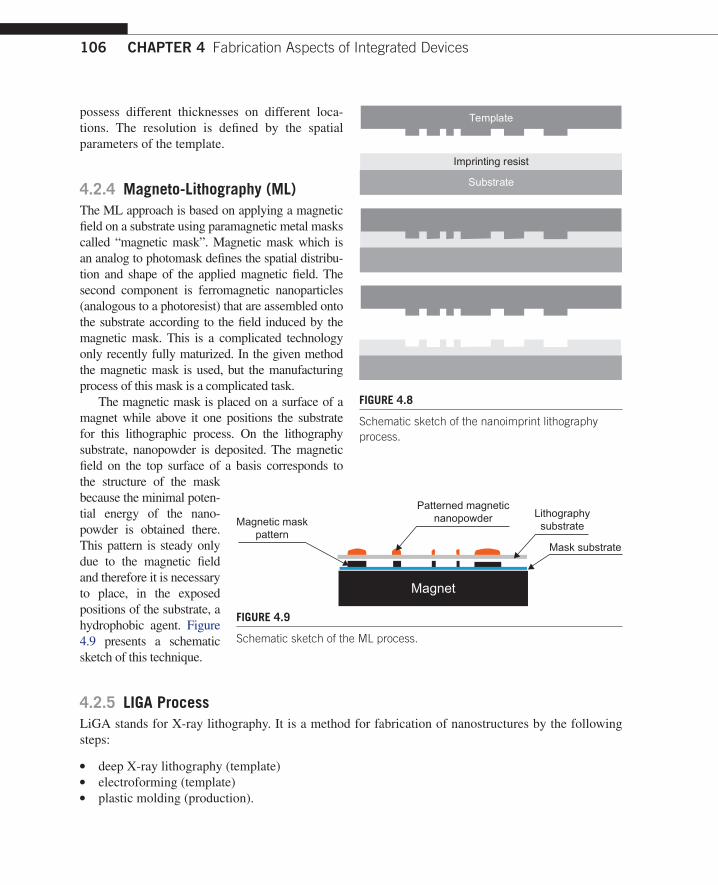
106 CHAPTER 4 Fabrication Aspects of Integrated Devices
possess different thicknesses on different loca-tions. The resolution is defined by the spatial parameters of the template.
4.2.4 Magneto-Lithography (ML)The ML approach is based on applying a magnetic field on a substrate using paramagnetic metal masks called “magnetic mask”. Magnetic mask which is an analog to photomask defines the spatial distribu-tion and shape of the applied magnetic field. The second component is ferromagnetic nanoparticles (analogous to a photoresist) that are assembled onto the substrate according to the field induced by the magnetic mask. This is a complicated technology only recently fully maturized. In the given method the magnetic mask is used, but the manufacturing process of this mask is a complicated task.
The magnetic mask is placed on a surface of a magnet while above it one positions the substrate for this lithographic process. On the lithography substrate, nanopowder is deposited. The magnetic field on the top surface of a basis corresponds to the structure of the mask because the minimal poten-tial energy of the nano-powder is obtained there. This pattern is steady only due to the magnetic field and therefore it is necessary to place, in the exposed positions of the substrate, a hydrophobic agent. Figure 4.9 presents a schematic sketch of this technique.
4.2.5 LIgA ProcessLiGA stands for X-ray lithography. It is a method for fabrication of nanostructures by the following steps:
l deep X-ray lithography (template)l electroforming (template)l plastic molding (production).
Substrate
Imprinting resist
Template
FIgURE 4.8
Schematic sketch of the nanoimprint lithography process.
Magnet
Mask substrate
Lithographysubstrate
Patterned magneticnanopowderMagnetic mask
pattern
FIgURE 4.9
Schematic sketch of the ML process.

107
This method is suitable for fabrication of nanostructures by steps of deep X-ray lithogra-phy, electroforming and plastic molding. This technology is suitable for low-cost mass pro-duction of micro-components.
Template fabrication in the LIGA process is done using X-ray lithography. But it is nec-essary to remember that the X-ray lithography only copies the mask to the template. Therefore, in all cases the formation of a picture starts from electron beam writing or from AFM lithography done over the mask.
When the X-ray mask is ready, the image of the mask is copied on the X-ray resist. Synchrotron radiation is used to transfer the lat-eral structural information from the mask into a plastic layer coated on top of the metal surface, normally polymethylmethacrylate (PMMA).
Exposure to radiation modifies the plastic material in such a way that it can be removed with a suit-able solvent, leaving behind the structure of the non-irradiated plastic (the “shadowed areas”) as the primary structure. The open locations on the surface are filled with metal, by means of electroform-ing. The X-ray resist is now removed. The procedure is described in Figure 4.10.
Now, when the template is fabricated, it is possible to make various nanostructures with low cost and a fast fabrication process while maintaining high accuracy. This may be possible by molding, nanoimprinting or other mass production methods.
This technology is applicable for mass production, when the nanostructure can be continuous. Its resolution is defined by the resolution of the mask and by the resolution of the e-beam writer.
This method is applicable for mass production of diffractive optical elements, mass production of photonics structures, mass production of micro- and nanosystems, organic and bio-organic circuits and micro- and nanofluidics.
4.2.6 Deposition with Lift-OffMany nanostructures can be fabricated by addition of a metal or an oxide layer on the electron resist pat-tern which is followed by lift-off stripping of the electron resist. There are many fields in surface nano chemistry that may be applied when the nano device is very thin, e.g. as thin as several molecular layers. These devices work due to surface charge modification, modification of the wetting properties of sur-faces, surface patterning using self-assembled mono layers (SAMs) etc.
First, by means of each one of the well-known methods of lithography, the desired image is transferred to the photo resist positioned on the substrate (see Fig. 4.11A). Then, the entire surface is coated with the desired material. It is possible to put liquid materials by wetting, and many solid materials by means of vacuum coating technologies. For example the case of wetting is seen in Figure 4.11B. The result obtained after drying is seen in Figure 4.11C. The next step that is described in Figure 4.11D includes removal of the resist.
PMMA
Metal substrate
(A)
(B)
(C)
FIgURE 4.10
(A) X-ray lithography. (B) Electroforming. (C) Removing the X-ray resist.
4.2 Methods to Pattern Surfaces

108 CHAPTER 4 Fabrication Aspects of Integrated Devices
This method provides very high resolution, but it is useful only for low aspect ratio applications, like surface chemistry, surface biology and others. Among its applications are molecular electronics – organic and bio-organic circuits, high-density optical memory, crystallization (colloidal crystals and bio-structures), nanoprinted catalysts, ultra-high-density oligonucleotide arrays – gene chips, sequenc-ing, pharmaceutical screening, micro- and nanofluidics, ultra-small, sensitive selective sensors and cryptography.
4.2.7 Focused Ion Beam (FIB)This is a method to pattern surfaces without the need for the image formation step. The FIB machine utilizes a focused beam of gallium ions that are operated at low-beam currents for imaging and at high-beam currents for site-specific milling.
Usually gallium is chosen because it is easy to build a gallium liquid metal ion source (LMIS). In gallium LMIS, gallium metal is placed in contact with a tungsten needle and heated. Gallium wets the tungsten, and a huge electric field (greater than 108 volts/cm) causes ionization and field emission of the gallium atoms. These ions are then accelerated to an energy of 5–50 KeV and then focused onto the sample by electrostatic lenses.
A modern FIB can deliver tens of nanoamps of current to a sample, or can image the sample with a spot size of the order of a few nm. The schematic sketch of this approach is seen in Figure 4.12. As seen the principle of the FIB is similar to the e-beam machine in that there is a source of ions then beam accelaration, directing and focusing components.
Liquid metalion source
Focusingsystem
Deflectingsystem
Wafer
Ion beam
FIgURE 4.12
Schematic sketch of the LMIS FIB.
Substrate
Resistpattern
Moistened surface
(A)
(B)
(C)
(D)
FIgURE 4.11
(A) Lithography. (B) Surface coating. (C) Drying. (D) Resist removal.

109
The characteristics of this approach include localized material removal on sub-100 nm scale, local-ized deposition of conducting and insulating layers in direct writing mode and process control by high-resolution secondary electron imaging.
The main applications include nanostructuring, mask and integrated circuit (IC) repairing, direct three-dimensional micro- and nanomachining, prototyping of photonics structures, prototyping of micro- and nanosystems, fast failure analysis and circuit modification, fabrication of solid-state nano-pores and nanostructuring using ion-induced self-organization processes.
4.3 APPLICATIONS OF NANOPHOTONICS AND NANOTECHNOLOgIESBelow we list several of the nanophotonic-related applications which can be realized by nanotechnol-ogy fabrication.
4.3.1 BiochipsA biochip is a collection of miniaturized test sites (microarrays) arranged on a solid substrate that permits many tests to be performed in parallel at the same time in order to achieve higher throughput. Biochips can also be used to perform techniques such as electrophoresis or polymerase chain reaction (PCR) using micro-fluidics technology.
4.3.2 Implantable Medical DevicesNanotechnology capabilities may be used for realizing implantable devices for medical applications. Some of those devices are directly related to integrated nanophotonic means. The types of devices that are currently being developed include:
l Implantable patient I.D./information microchipsl Implantable cardioverter-defibrillators and pacemakersl Implantable visual sensory aids and hearing devicesl Implantable stimulators – brain/nerves/bladder, etc.l Implantable drug administration and pain control devicesl Implantable sensors and/or active monitoring devicesl Nano generators for heart-related medical treatmentl Nanoporous ceramic membranesl Prosthetic devices such as neural prosthetic devices or biological control of prosthetic devicesl Electronic pills that can collect data from a patient’s body and wirelessly send it to a nearby devicel Surgical and medical devices, e.g. nano-amorphous coatings for medical instrumentsl Implantable biosensors for trauma monitoring in the event of mass casualties.
4.3.3 Artificial OrgansAn artificial organ is a man-made device that is implanted into, or integrated onto, a human to replace a natural organ, for the purpose of restoring a specific function or a group of related functions so the
4.3 Applications of Nanophotonics and Nanotechnologies

110 CHAPTER 4 Fabrication Aspects of Integrated Devices
patient may return to as normal a life as possible. The replaced function does not necessarily have to be related to life support, but often is.
Nano- and micro-machining techniques are the important core technology for the development of the artificial internal organs due to the limited available space. Various kinds of artificial internal organ development are ongoing and include artificial esophagus, artificial sphincter, artificial heart, ventricular assist devices, artificial myocardium system and epilepsy control machine.
4.3.4 Molecular MotorsMolecular motors are biological molecular machines that are the essential agents of movement in liv-ing organisms. Generally speaking, a motor may be defined as a device that consumes energy in one form and converts it into motion or mechanical work. Many protein-based molecular motors harness the chemical free energy released by the hydrolysis of adenosine triphosphate (ATP) in order to per-form mechanical work.
One important difference between molecular motors and macroscopic motors is that unlike macro-scopic motors the molecular motors operate in a thermal bath, an environment where the fluctuations due to thermal noise are significant.
4.3.5 Molecular ElectronicsMolecular electronics is an interdisciplinary theme that spans physics, chemistry, and materials sci-ence. The unifying feature of this area is the use of molecular building blocks for the fabrication of electronic components, both passive (e.g. resistive wires) and active (e.g. transistors). Molecular electronics provides a means to extend Moore’s law beyond the foreseen limits of small-scale conven-tional silicon integrated circuits.
4.3.6 BiosensorsBiosensors are powerful tools aimed at providing selective identification of toxic chemical com-pounds at ultra-low trace levels in industrial products, chemical substances, environmental samples (e.g. air, soil and water) or biological systems (e.g. bacteria, virus or tissue components) for biomedi-cal diagnosis. Combining the exquisite specificity of biological recognition probes and the excellent sensitivity of laser-based optical detection, biosensors are capable of detecting and differentiating big/chemical constituents of complex systems in order to provide unambiguous identification and accu-rate quantification.
Examples of such sensors are cell-based neurotoxicity array biosensors, electronic NOSE (natural olfactory sensor emulator) for trauma monitoring, DNA biochips for brain tumor cancer diagnostics and prognostics, sub-cellular monitoring using nano-biosensors and nano-beacons, antibody-based fluoro-immuno-sensors, cancer diagnostics using laser-induced fluorescence, etc.
4.3.7 NanosensorsAs a direct continuation of the previously discussed application, the field of nanosensors includes explor-ing the sanctuary of an individual living cell. The combination of nanotechnology, biology, advanced
111
materials and photonics opens the possibility of detecting and manipulating atoms and molecules using nanodevices which have the potential for a wide variety of medical uses at the cellular level.
Nanosensors include acoustic and ultrasound techniques for monitoring brain injuries, plasmon-ics which refers to the research area of enhanced electromagnetic properties of metallic nanostruc-tures, hyper-spectral surface-enhanced Raman imaging for monitoring the intracellular distribution of molecular species associated with biological abnormalities and localization of drugs and other cellu-lar components within cells, near-field scanning optical microscopy (NSOM), etc.
Currently optical nanobiosensors are integrated into nanoscale devices consisting of a biological recognition molecule coupled to the optical transducing element such as an optical nanofiber inter-faced to a photometric detection system. Those devices are capable of providing specific quantitative, semi-quantitative or qualitative analytical information using biological recognition elements (e.g., DNA, protein) in direct spatial contact with a solid-state optical transducer element [1].
4.3.8 Solar CellsPlasmonic excitation in metal nanostructures is a promising way of increasing the light absorp-tion in thin-film solar cells. Enhancements in photocurrent have been observed for a wide range of semiconductors and solar cell configurations. When silver particles were deposited on 1.25 m thick silicon-on-insulator solar cells overall photocurrent increased by 33%. In addition several designs of nanophotonic structures have been proposed and demonstrated to improve light collection efficiency. In fact the light scattering and trapping by the nanoparticles is one of the mechanisms that enhances the light collection efficiency. The other mechanism for enhancement is related to the near-field enhancement which by the end means larger local concentration of light. This topic is under extensive study and was reviewed recently by several investigators [2].
References [1] I. Abdulhalim, M. Zourob, A. Lakhtakia, Overview of optical biosensing techniques, in Handbook
of Biosensing and Biochips , R.S. Marks, C.R. Lowe, D.C. Cullen, H.H. Weetall, I. Karube (Eds.), John Wiley and Sons, 2007; ISBN 978-0-470-01905-4.
[2] K.R. Catchpole, A. Polman, Plasmonic solar cells, Opt. Express 16 (2008) 21793–21800.
References

113Integrated Nanophotonic Devices. DOI:© 2010 Elsevier Inc. All rights reserved.
10.1016/B978-1-4377-7848-9.00005-72010
CHAPTER OUTLINE HEAD
5.1 Hybrid Opto-Electronic Approaches ..................................................................................................1145.1.1 Electro-Optic-on-Chip Bragg Modulator ...................................................................... 1145.1.2 Photo Initiated On-Chip Modulator ............................................................................ 120
5.1.2.1 Device Operation Modes .........................................................................................1205.1.2.2 Fabrication Process ................................................................................................1225.1.2.3 Experimental Characterization and Interpretation .....................................................125
5.2 All-Optical Plasma Dispersion Effect-Based Approach .......................................................................1275.2.1 Technical Description ............................................................................................... 1285.2.2 Experimental Characterization ................................................................................... 129
5.3 Particle Trapping-Based Modulation .................................................................................................1365.3.1 Introduction ............................................................................................................ 1365.3.2 All-Optical Nanomodulator, Sensor, Wavelength Converter, Logic Gate and
Flip-Flop ................................................................................................................. 1365.3.2.1 Theoretical Background ..........................................................................................1375.3.2.2 Fabrication of Devices .............................................................................................1385.3.2.3 Devices and Simulation Results ..............................................................................1395.3.2.4 Preliminary Experimental Validations .......................................................................141
5.3.3 Electro-Optical Modulator ......................................................................................... 1445.3.3.1 Simulations .............................................................................................................1445.3.3.2 Fabrication .............................................................................................................1475.3.3.3 Experimental Testing ...............................................................................................147
5.3.4 Tunable Nanodevices Fabricated by Controlled Deposition of Gold Nanoparticles Via Focused Ion Beam .............................................................................................. 1495.3.4.1 Patterning Method ..................................................................................................1495.3.4.2 Experimental Result ................................................................................................149
5.3.5 Self-Assembly of Nanometric Metallic Particles for Realization of Photonic and Electronic Nanotransistors ........................................................................................ 152
5.3.6 Design and Fabrication of 1X2 Nanophotonic Switch ................................................... 1545.3.6.1 Numerical Simulations ............................................................................................1555.3.6.2 Fabrication and Realization .....................................................................................159
5.4 All-Optical Integrated Micrologic Gate ..............................................................................................1595.4.1 Operation Principle .................................................................................................. 1615.4.2 Fabrication .............................................................................................................. 1625.4.3 Experimental Testing ................................................................................................ 163
Non-Conventional Modulation Schemes 5
CHAPTER

114 CHAPTER 5 Non-Conventional Modulation Schemes
In this chapter we intend to present several non-conventional silicon-based integrated circuits realizing optical modulators as well as other functionalities such as logic gates. Although the presented concepts are in the state of pure research and yet far from being industrially implemented, they show the potential as well as a different point of view of how to allocate existing resources for achieving the desired goal.
5.1 HyBRID OPTO-ELECTRONIC APPROACHEs5.1.1 Electro-Optic-on-Chip Bragg ModulatorFollowing Eq. 2.16 the refractive index n and the absorption coefficient vary due to the change in con-centration of electrons and holes. Proper external voltage that is applied over the gate of the MOS capac-itor can cause an inversion, i.e. generation of mobile carriers that accumulate near the surface between the oxide and the semiconductor. In p-type silicon, the free carriers in the inversion layer are electrons. The concentration of those free carriers is high. The free carrier density at the surface, ns, is given by:
n n xn
N
q x
kT
n
Nsi
a
i
as= = =
=( )
= [ ]( ) exp
( )exp ,0
02 2
(5.1)
where s is the potential at the interface between the silicon and the oxide (also called surface poten-tial), q/kT (q is the charge of the electron, k is the Boltzmann constant and T is the temperature), Na is the concentration of the acceptors, and ni is the intrinsic concentration of free charges in silicon.
The device presented generates an MOS capacitor in which the semiconductor is the single-mode sili-con core that guides the light and the metal contact is the periodically patterned electrode [1]. The device uses the effect of the high concentration of free carriers in the inversion layer and the fact that the inversion is axially periodic due to the way the electrodes are constructed in order to enhance the modulation ratio and its effect over the beam that is traveling through the single-mode core. The overview of the proposed device is seen in Figure 5.1. The horizontal as well as the vertical units are in meters. The axial period of the patterned electrode fits the Bragg condition for the wavelength of the information photons:
=
2neff
(5.2)
where is the central wavelength of the beam and neff is the effective refraction index of silicon that satisfies π = 2 0neff / , where is the wave number in the propagation axis parallel to the waveguide. In order to reduce photonic losses the electrodes are realized with indium-tin-oxide (ITO) which is an optically transparent and electrically conductive material.
5.5 Polarizing and spectrally selective Photonic Device Based Upon Dielectric Nanorods ........................1655.5.1 Fabrication Process .................................................................................................. 1655.5.2 Experimental Testing ................................................................................................ 1675.5.3 Preliminary Results and Discussion ........................................................................... 169
References ............................................................................................................................................170

115
The design and simulation of the proposed concept was done using COMSOL Multiphysics. COMSOL Multiphysics is commercial software that solves partial differential equations via the finite ele-ment method. TM mode in 2-D was solved for a wavelength of 1.55 m as the optical information carrier.
The simulation parameters follow a silicon waveguide width of 200 nm and height of 450 nm with refractive index of 3.48. The inversion layer thickness is 10 nm the thickness of the oxide having a refractive index of 1.45 is 50 nm. Those dimensions were chosen to enable low mode overlap between the silicon waveguide and the ITO on one hand while maintaining high surface potential on the other hand. The assumed acceptor concentration was 4 × 1015 cm−3. Note that the 50 nm thickness of the oxide was carefully chosen according to the tradeoff between the overlapping of the optical mode and the inversion layer versus the surface potential. While a wide SiO2 region extends the overlap of the optical mode with the inversion layer, the applied surface potential, which defines the free electron concentration, will be reduced.
The 10 nm width of the inversion layer was computed as follows: the position at which the elec-tron density reduces to 25% of its maximum value at the surface was estimated. Denoting this con-centration as nx one can use Eq. 5.1 to determine the potential x that is obtained at x which is the position of the end of the inversion layer. To calculate x one may use the following relation:
xA
p
ne ep
p
x s
= ⋅
−
− −1 20
0
2 2
(5.3)
Single modeinput light
λ/4 inversion layers generated when voltage is applied
SiO2
SiO2
Λ
λ/4 inversion layers generated when voltage applied
x
y
z
0.5
3
phi_s(6) = 0.935 Surface: Magnetic field,z component [A/m]
2.5
2
1.5
1
0.5
0
−0.5
−1
−1.5
−2
−2.5
−3
1 1.5 2 2.5 3 3.5 4 4.5 5 5.5 6 6.5 7×10−6
×10−7
−1.5
−1
−0.5
0
0.5
1
1.5
Max: 1.996
7.5Min: −1.513
FIGURE 5.1
The overview of the proposed device: Light propagating through the proposed structure.
5.1 Hybrid Opto-Electronic Approaches

116 CHAPTER 5 Non-Conventional Modulation Schemes
where
AkT
q LL
q pdd
s
p
=⋅
≡⋅ ⋅
2
0
, ε
(5.4)
with np0, pp0 as the concentration of the mobile electrons and holes respectively in the p-type semi-conductor in steady state.
Figures 5.2A and 5.2B present the simulation for the propagation of the magnetic component of the field through the device. The 200 nm silicon waveguide in the middle is guiding a single mode
(C)y [m] – Waveguide cross section
0 200 nm 400 nm−200 nm−400 nm
HZ mode profile
Mag
netic
fiel
d [A
/m]
0
0.2
0.4
0.6
0.8
1
Inversionlayer overlap
(A)
0 1 2 3 4
×10−6
×10−5
−0.5
0
0.5
1
1.5
−2
−1
0
1
2
phi_s(1) = 0 Surface: Magnetic field,z component [A/m]
(B)
−0.5
0
0.5
1
−1
0 1 2 3 4
×10−6
×10−5
−2
−1
0
1
2
phi_s(6) = 0.935 Surface: Magnetic field,z component [A/m]
1.5
FIGURE 5.2
Numerical simulation of the propagated magnetic field. (A) The control voltage is OFF. (B) The control voltage is ON. (C) The cross-section of the propagated mode.
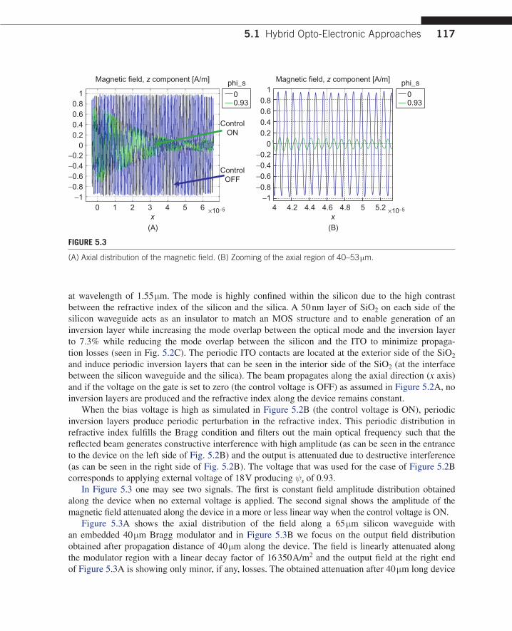
117
at wavelength of 1.55 m. The mode is highly confined within the silicon due to the high contrast between the refractive index of the silicon and the silica. A 50 nm layer of SiO2 on each side of the silicon waveguide acts as an insulator to match an MOS structure and to enable generation of an inversion layer while increasing the mode overlap between the optical mode and the inversion layer to 7.3% while reducing the mode overlap between the silicon and the ITO to minimize propaga-tion losses (seen in Fig. 5.2C). The periodic ITO contacts are located at the exterior side of the SiO2 and induce periodic inversion layers that can be seen in the interior side of the SiO2 (at the interface between the silicon waveguide and the silica). The beam propagates along the axial direction (x axis) and if the voltage on the gate is set to zero (the control voltage is OFF) as assumed in Figure 5.2A, no inversion layers are produced and the refractive index along the device remains constant.
When the bias voltage is high as simulated in Figure 5.2B (the control voltage is ON), periodic inversion layers produce periodic perturbation in the refractive index. This periodic distribution in refractive index fulfills the Bragg condition and filters out the main optical frequency such that the reflected beam generates constructive interference with high amplitude (as can be seen in the entrance to the device on the left side of Fig. 5.2B) and the output is attenuated due to destructive interference (as can be seen in the right side of Fig. 5.2B). The voltage that was used for the case of Figure 5.2B corresponds to applying external voltage of 18 V producing s of 0.93.
In Figure 5.3 one may see two signals. The first is constant field amplitude distribution obtained along the device when no external voltage is applied. The second signal shows the amplitude of the magnetic field attenuated along the device in a more or less linear way when the control voltage is ON.
Figure 5.3A shows the axial distribution of the field along a 65 m silicon waveguide with an embedded 40 m Bragg modulator and in Figure 5.3B we focus on the output field distribution obtained after propagation distance of 40 m along the device. The field is linearly attenuated along the modulator region with a linear decay factor of 16 350 A/m2 and the output field at the right end of Figure 5.3A is showing only minor, if any, losses. The obtained attenuation after 40 m long device
4−1
−0.8−0.6−0.4−0.2
00.20.40.60.8
1
−1−0.8−0.6−0.4−0.2
00.20.40.60.8
Magnetic field, z component [A/m] Magnetic field, z component [A/m] phi_s
00.93
1
4.2 4.4 4.6x
(A) (B)
4.8 5 5.20 1 2 3x
4 5 6 ×10−5 ×10−5
phi_s
00.93
ControlON
ControlOFF
FIGURE 5.3
(A) Axial distribution of the magnetic field. (B) Zooming of the axial region of 40–53 m.
5.1 Hybrid Opto-Electronic Approaches

118 CHAPTER 5 Non-Conventional Modulation Schemes
is of 1:10 in field and 1:100 in intensity. This attenuation (20 dB) is obtained with external voltage of 18 V producing s of 0.93 (see Eq. 5.1).
Figure 5.4 presents the Poynting vector propagating in the device for the case of no modulation (non-attenuated signal) and for external voltage in its ON state, i.e. with mod-ulation command (the two attenuated signals plotted one on opt of the other). One may see that external voltage yielding s of 0.93 results, after a device of only 20 m, in attenuation of 13 dB in intensity (in the amplitude of vector Poynting).
The modulation depth is strongly affected by the voltage applied on the silicon oxide interface. The greater the voltage, the higher is
the change in the refraction index n that is produced in the periodic inversion layers. Therefore for a given and desired contrast of modulation, the length of the device is to be determined by the maximal allowed level of the applied modulation voltage.
As seen from Figure 5.4, the propagation of the Poynting vector for external voltage producing s of 0.93 and 0.94 yields significantly different modulation contrast: changing s from 0.93 to 0.94 changes the obtained modulation contrast, after 20 m of propagation through the device, by an addi-tional factor of 4.
In the simulations shown in Figure 5.5 the spectral response of the proposed device was tested and its performance was compared with controllable ring resonator as proposed by Ref. [62].
In Figure 5.5A the Bragg-based modulator was simulated (when the modulation is ON) and its spectral response after propagation length of 30 m and external voltage producing s of 0.92 was presented. One may see that an extinction ratio of about 7 dB with spectral bandwidth of about 15 nm is obtained. In Figure 5.5B the ring resonator with the parameters appearing in Ref. [62] (ring dia-meter of 10 m and Q of 7700) was simulated. This resonator which obtained similar extinction ratio had much narrower spectral bandwidth of less than 0.1 nm (which is about 12.5 GHz). Thus, the pro-posed device can operate with larger spectral bandwidth and may fit better to the DWDM optics com-munication grid.
Note that although the ring resonator had Q factor of 7700 (it required an effectively long opti-cal path to obtain the extension ratio of 7 dB) its area is larger than the area occupied by the proposed technique (80 m2 for the ring resonator in comparison to 9 m2 for the proposed Bragg-based device).
Note also that the translation between s and the required external voltage is such that s of 0.92, 0.93 and 0.94 is obtained with external voltage of approximately 15, 18 and 22 volts respectively. This was computed using the relations taken from Ref. [2].
The inherent tradeoff of the device is between its modulation depth and its length as well as power consumption and modulation speed. The operating voltages can be reduced with a longer device to obtain the same modulation depth. However, a DC offset that can be constantly applied can reduce the
phi_s
−13 dB
120 00.930.94
100
80
60
40
20
0
Hz*
Ey_
emw
e [W
/m2 ]
Hz*Ey_emwe [W/m2]
−20
−40
−60−0.5 0 0.5 1 1.5
x �10−52 2.5 3 3.5 4
FIGURE 5.4
Poynting vector propagation.
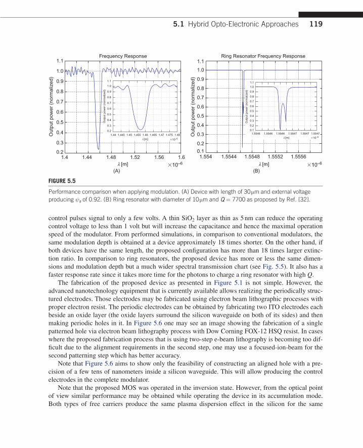
119
control pulses signal to only a few volts. A thin SiO2 layer as thin as 5 nm can reduce the operating control voltage to less than 1 volt but will increase the capacitance and hence the maximal operation speed of the modulator. From performed simulations, in comparison to conventional modulators, the same modulation depth is obtained at a device approximately 18 times shorter. On the other hand, if both devices have the same length, the proposed configuration has more than 18 times larger extinc-tion ratio. In comparison to ring resonators, the proposed device has more or less the same dimen-sions and modulation depth but a much wider spectral transmission chart (see Fig. 5.5). It also has a faster response rate since it takes more time for the photons to charge a ring resonator with high Q.
The fabrication of the proposed device as presented in Figure 5.1 is not simple. However, the advanced nanotechnology equipment that is currently available allows realizing the periodically struc-tured electrodes. Those electrodes may be fabricated using electron beam lithographic processes with proper electron resist. The periodic electrodes can be obtained by fabricating two ITO electrodes each beside an oxide layer (the oxide layers surround the silicon waveguide on both of its sides) and then making periodic holes in it. In Figure 5.6 one may see an image showing the fabrication of a single patterned hole via electron beam lithography process with Dow Corning FOX-12 HSQ resist. In cases where the proposed fabrication process that is using two-step e-beam lithography is becoming too dif-ficult due to the alignment requirements in the second step, one may use a focused-ion-beam for the second patterning step which has better accuracy.
Note that Figure 5.6 aims to show only the feasibility of constructing an aligned hole with a pre-cision of a few tens of nanometers inside a silicon waveguide. This will allow producing the control electrodes in the complete modulator.
Note that the proposed MOS was operated in the inversion state. However, from the optical point of view similar performance may be obtained while operating the device in its accumulation mode. Both types of free carriers produce the same plasma dispersion effect in the silicon for the same
(A) (B)
1.4
1.0
Out
put p
ower
(no
rmal
ized
)
0.2
0.3
0.4
0.5
0.6
0.7
0.8
0.9
1.1
1.44 1.48 1.52 1.56 1.6λ [m] �10–6
Frequency Response
Out
put p
ower
(no
rmal
ized
)
1.44 1.445 1.45 1.455 1.46 1.465 1.47 1.475 1.48
λ [m]
0.2
0.3
0.4
0.5
0.6
0.7
0.8
0.9
1.0
1.1
Ring Resonator Frequency Response
Out
put p
ower
(no
rmal
ized
)
0.1
0.2
0.3
0.4
0.5
0.6
0.7
0.8
0.9
1.0
1.1
1.554 1.5544 1.5548 1.5552 1.5556
λ [m] �10–6
Out
put p
ower
(no
rmal
ized
)
1.5546 1.5546 1.5546 1.5547 1.5547 1.5547
�10–6�10–6
0.2
0.1
0.3
0.4
0.5
0.6
0.7
0.8
0.9
1.0
1.1
λ [m]
FIGURE 5.5
Performance comparison when applying modulation. (A) Device with length of 30 m and external voltage producing s of 0.92. (B) Ring resonator with diameter of 10 m and Q = 7700 as proposed by Ref. [32].
5.1 Hybrid Opto-Electronic Approaches

120 CHAPTER 5 Non-Conventional Modulation Schemes
change in concentration. To illustrate this, Figure 5.7 presents the change in the refraction index due to free holes and free electrons. One may see that the change is more or less the same and thus there is no significant difference in the optical effect made by the two types of free carriers.
Nevertheless, it is known that the majority of free carriers have faster response times than minor-ity carriers. Although this may be solved in various electronic “tricks”, in most cases in silicon it is preferable to work with majority carriers, i.e. in accumulation mode.
5.1.2 Photo Initiated On-Chip ModulatorIn this subsection we present the realization of a hybrid type of modulator in which the information is electronic while the control commands that determine whether this information will go through are photonics. The usage of photonic control command has the advantage of realizing faster response times since no electronic delay constant of RC is generated. The name of the proposed working con-cept is Semiconductor On Insulator (SOI) Photo Activated Modulator (PAM).
5.1.2.1 Device Operation Modes5.1.2.1.1 The SOI-PAM Without Illumination – Open (ON) StateAs depicted in Figure 5.8A the device consists of an information channel (n-type silicon) supplied with source and drain potentials which are denoted as VS and VD (the source is connected to ground). The channel is insulated from the substrate by a 150-nm-thick buried oxide layer. A negative gate potential VG is applied to the bottom side of the p-type substrate such that a negatively charged depletion layer appears under the buried oxide layer. Consequently, a positively charged depletion layer is generated inside the n-type channel (source terminal is connected to ground) as shown in
Concentration [cm–3]10170
0.01
0.02
0.03
0.04
Cha
nge
in r
efra
ctio
n in
dex
0.05
0.06
0.07
0.08
0.09ElectronsHoles
1018 1019 1020
FIGURE 5.7
The change in the refraction index due to free holes and free electrons.
1 µm
Si
SiO2
FIGURE 5.6
Pre-fabrication feasibility.
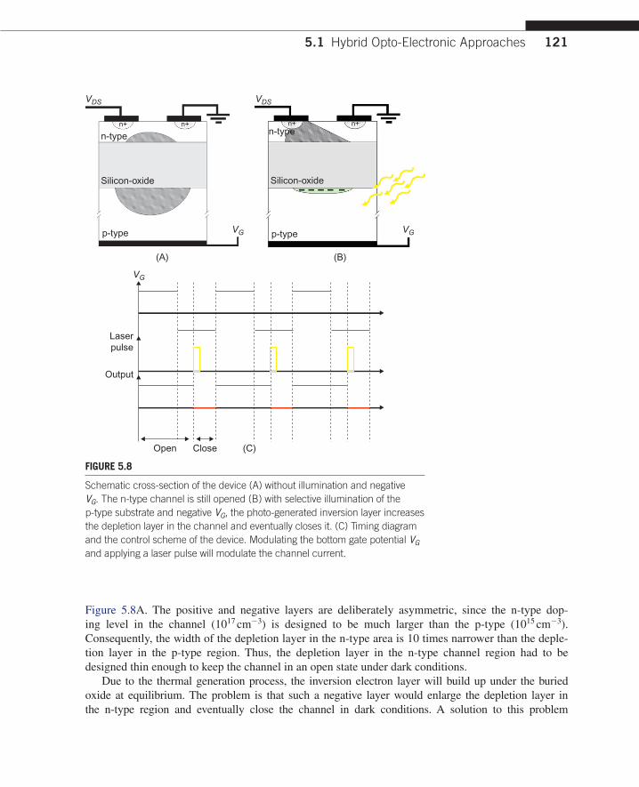
121
Figure 5.8A. The positive and negative layers are deliberately asymmetric, since the n-type dop-ing level in the channel (1017 cm−3) is designed to be much larger than the p-type (1015 cm−3). Consequently, the width of the depletion layer in the n-type area is 10 times narrower than the deple-tion layer in the p-type region. Thus, the depletion layer in the n-type channel region had to be designed thin enough to keep the channel in an open state under dark conditions.
Due to the thermal generation process, the inversion electron layer will build up under the buried oxide at equilibrium. The problem is that such a negative layer would enlarge the depletion layer in the n-type region and eventually close the channel in dark conditions. A solution to this problem
5.1 Hybrid Opto-Electronic Approaches
VDS
n-type
Silicon-oxide
p-type VG
n+ n+
VDS
n-type
Silicon-oxide
p-type VG
n+ n+
VG
Laserpulse
Output
Open Close
(A) (B)
(C)
FIGURE 5.8
Schematic cross-section of the device (A) without illumination and negative VG. The n-type channel is still opened (B) with selective illumination of the p-type substrate and negative VG, the photo-generated inversion layer increases the depletion layer in the channel and eventually closes it. (C) Timing diagram and the control scheme of the device. Modulating the bottom gate potential VG and applying a laser pulse will modulate the channel current.

122 CHAPTER 5 Non-Conventional Modulation Schemes
consists from applying a rapid modulation of the gate potential VG creating a deep depletion layer in the p-type area under the buried oxide. Since the inversion layer could not be sustained under these non-equilibrium conditions, the device behaves like an MOS capacitor in its deep depletion state [3,4].
5.1.2.1.2 The SOI-PAM Under Illumination – Closed (OFF) StateIn the presented device, the closed state occurs when the modulated gate voltage VG is negative. By synchronously illuminating the p-type area, the free photo-generated electron concentration can be significantly and instantly increased (see Fig. 5.8B) until the inversion state is reached. As a result, the voltage drop on the p-type silicon is reduced, consequently the voltage drop on the n-type layer is increased. As a result, the depletion layer in the n-type channel is widely extended and eventually closes the channel. Under these conditions, the “dynamic” inversion layer is sustained by applying external illumination.
That inversion layer is sustained until positive voltage is applied on the gate contact. Once the illumi-nation is decreased, thermal generation takes place and eventually creates an inversion layer that could also close the channel. However, if the modulation rate of VG is high enough the thermal generation would not be efficient because of its relatively long time response constant. So, the device remains in deep depletion till the next illumination pulse. This principle reminds us of effects encountered in CCD devices.
A time diagram describing the timing and the control scheme of the proposed device is depicted in Figure 5.8C.
5.1.2.2 Fabrication ProcessThe device requires a very thin n-type (SOI) layer with p-type substrate. The starting material is an SOI wafer with silicon layer thickness of about 30 nm and n-type doping of 1017 cm−3. The thickness of the buried insulator oxide is about 150 nm and the p-type silicon substrate has a doping concentra-tion of 1015 cm−3.
First of all, thin layers of oxide and nitride are grown and deposited respectively on the SOI wafer. After the photolithography step and etch of the oxide–nitride layers, the surrounding silicon is fully oxidized down to the buried oxide by the LOCal Oxidation of Silicon (LOCOS) process. This step creates the desired thick oxide that isolates the channel from the lateral photo-generated current.
The next step is to connect the external source and drain voltages to their respective areas in the channel. This connection is ensured by depositing a polysilicon layer using a Low-Pressure Chemical Vapor Deposition process (LPCVD) followed by doping the polysilicon layer with a very high phos-phor concentration. Indeed, direct deposition of aluminum on the n-type channel would lead to a non-ohmic Schottky contact. Subsequently, Phosphor doped Silicon Glass (PSG) is grown on the polysilicon layer. Then, a thermal annealing is performed in order to diffuse the phosphor down to the channel through the polysilicon layer, making n+ ohmic contact. Illustrations of the device are shown before and after the PSG and polysilicon etch steps in Figures 5.9A and 5.9B, respectively.
One can see a zoom image of the single device (Fig. 5.9) in Figure 5.10A. A corresponding tilted image obtained by Scanning Electron Microscopy (SEM) is presented in Figure 5.10B. The nitride and the Al are not seen in the figure since they are too thin.
The illumination should close the information channel in order to limit the absorption in silicon. In order to enable a laser illumination to reach the p-type substrate under the buried oxide, a V-groove is etched by an anisotropic wet KOH technique [5,6]. The groove area is defined by photolithography
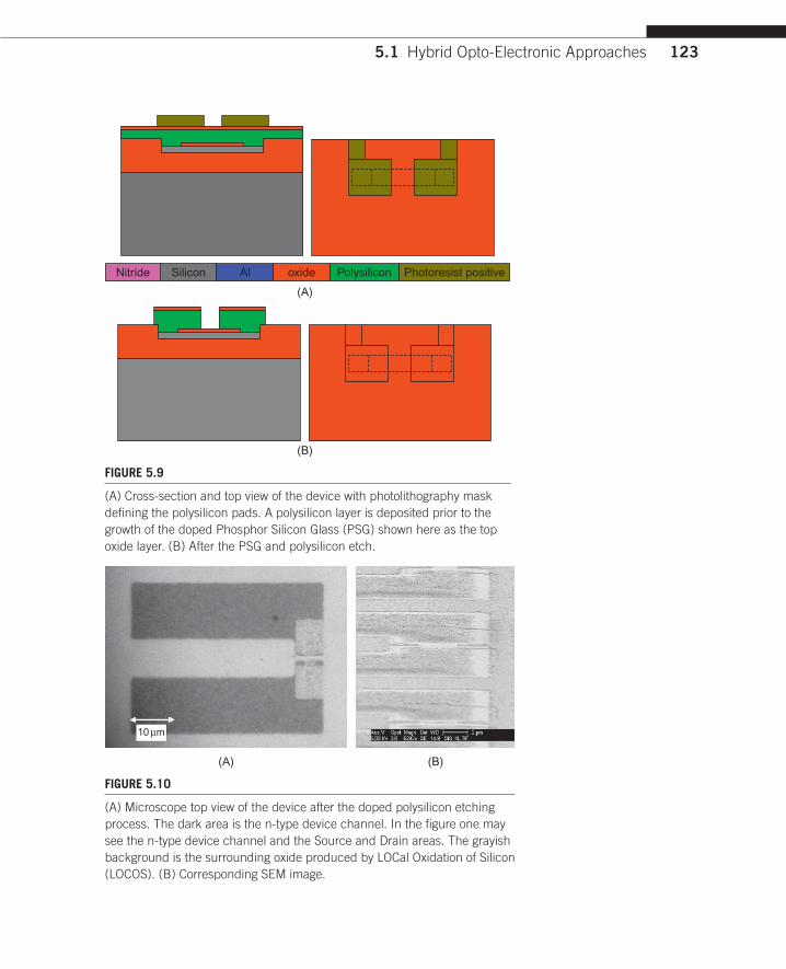
123
(A)
(B)
Nitride Silicon Al oxide Polysilicon Photoresist positive
FIGURE 5.9
(A) Cross-section and top view of the device with photolithography mask defining the polysilicon pads. A polysilicon layer is deposited prior to the growth of the doped Phosphor Silicon Glass (PSG) shown here as the top oxide layer. (B) After the PSG and polysilicon etch.
5.1 Hybrid Opto-Electronic Approaches
10 µm
(A) (B)
FIGURE 5.10
(A) Microscope top view of the device after the doped polysilicon etching process. The dark area is the n-type device channel. In the figure one may see the n-type device channel and the Source and Drain areas. The grayish background is the surrounding oxide produced by LOCal Oxidation of Silicon (LOCOS). (B) Corresponding SEM image.
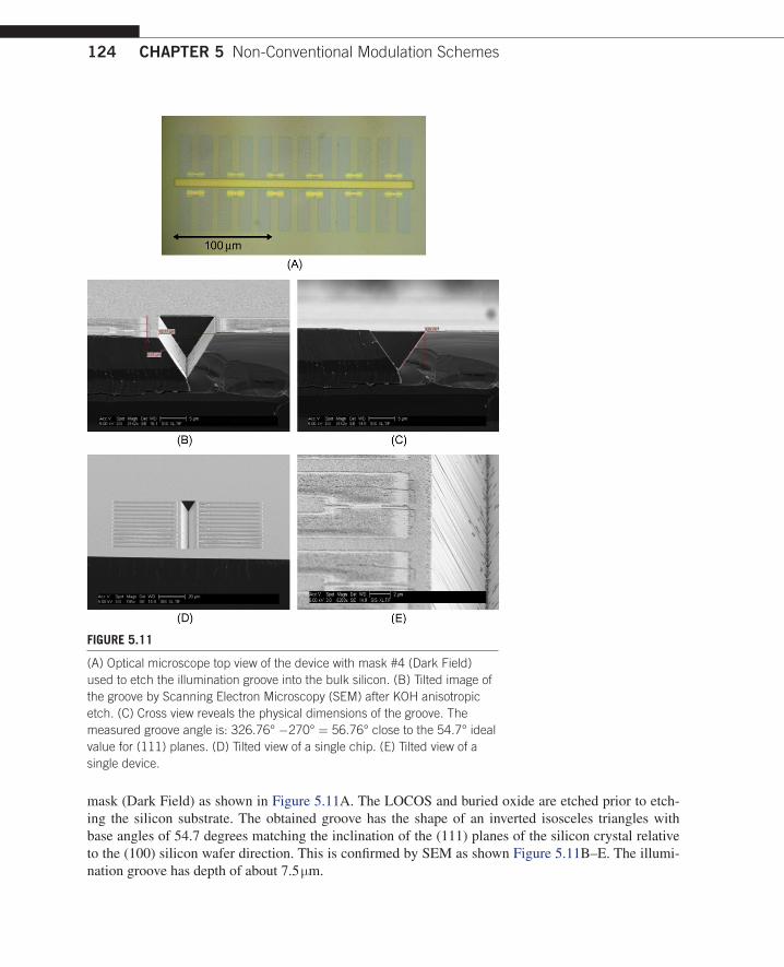
124 CHAPTER 5 Non-Conventional Modulation Schemes
mask (Dark Field) as shown in Figure 5.11A. The LOCOS and buried oxide are etched prior to etch-ing the silicon substrate. The obtained groove has the shape of an inverted isosceles triangles with base angles of 54.7 degrees matching the inclination of the (111) planes of the silicon crystal relative to the (100) silicon wafer direction. This is confirmed by SEM as shown Figure 5.11B–E. The illumi-nation groove has depth of about 7.5 m.
FIGURE 5.11
(A) Optical microscope top view of the device with mask #4 (Dark Field) used to etch the illumination groove into the bulk silicon. (B) Tilted image of the groove by Scanning Electron Microscopy (SEM) after KOH anisotropic etch. (C) Cross view reveals the physical dimensions of the groove. The measured groove angle is: 326.76° −270° = 56.76° close to the 54.7° ideal value for (111) planes. (D) Tilted view of a single chip. (E) Tilted view of a single device.

125
After opening holes for contacts into the silicon oxide, aluminum lines connecting the polysilicon doped pads to peripheral pads of the chip were defined. This was done by wet aluminum etching. Photoresist removal and backside metallization complete the process. A perspective drawing and an optical microscope top view of the completed chip are given in Figure 5.12.
5.1.2.3 Experimental Characterization and InterpretationThe device was packaged on a DIP socket. Electrical characterization was performed using a com-mercial test-fixture. A pulse generator is connected to the gate back-contact while the drain contact was connected to a constant power supply (+3 V). The source is maintained at common ground potential. The drain current behavior is monitored using a multichannel digital oscilloscope connected to a serial resistance of 90 Kohm. The low and high levels of the gate pulse were set to –3 V and +3 V, respectively.
5.1 Hybrid Opto-Electronic Approaches
Top illuminationPolysilicon padembedded in oxide
Channel embeddedin oxide
Aluminum interconnectdeposited on oxide
Buried oxideV-groove
p-type silicon substrate
Back side metallization
(A)
(B)
FIGURE 5.12
(A) Perspective view of the final device with the side groove allowing top illumination. (B) Optical microscope top view of the completed chip.

126 CHAPTER 5 Non-Conventional Modulation Schemes
By using a green diode laser triggered and modulated by the pulse generator, the influence of the laser pulse illumination on the drain current can be measured and compared to a dark situation.
For a pulse frequency of 50 KHz, the following behavior was observed (see Fig. 5.13A):
1. During the short (1 s) positive gate level (+3 V), the drain current is instantly raised to the high level (5 A). Indeed, in this case, all the minority electrons in the silicon substrate near the bottom
−2 −1 0 1 2 3 4
� 10−5
� 10−5 � 10−5
−1
0
1
2
3
4
5
6
7
I D[µ
A]
−3
–3
0
3
Time [sec]
V[V
]
VG
Illumination
ID without the illumination
ID with the illumination
(A)
0 0.5 1 1.5 2 0 0.5 1 1.5 20
0.2
0.4
0.6
0.8
1
1.2
1.4
1.6
1.8
2
Time [sec]
I D[µ
A]
ID without the illumination
ID with the illumination
Illumination
10-4
10-3
10-2
100
Time [sec]
I D[µ
A]
ID without the illumination
ID with the illumination
Illumination
(B)
FIGURE 5.13
Experimental characterization of the fabricated device. (A) Experimental results obtained when applying periodic pulses on VG and illuminating the device in the negative level of VG. (B) Zoom to the measurements obtained in one period. Left: linear scale. Right: logarithmic scale.

127
of the buried oxide layer recombine instantly with the injected majority holes. Moreover, the short pulse width prevents the formation of a thermal inversion layer in the p-type substrate in the dark condition. Consequently the channel is still opened.
2. During the long (19 s) negative gate level (–3 V) width and in dark condition the drain current is decreased steeply to a low but non-zero level (1 A). By applying a laser pulse illumination of 10 s width having a 5 s delay relative to the raising edge of gate pulse, a significant reduction of the drain current by two orders of magnitude to practical zero level is observed (see Fig. 5.13B). a. In the dark, the drain current steep drop is due to the instant expansion of the positive depleted
layer in the n-type channel. This layer is induced by the deep-depletion negative layer located in the p-type substrate below the buried oxide that is instantly created by the negative gate level. However, this extension is not sufficient to close the channel completely, leading to the 1 A dark current. Since the pulse is at relatively high frequency (50 kHz), the slow thermal generation of the electron inversion layer cannot contribute to close the channel in the dark condition.
b. During illumination, the inversion layer can be generated instantly due to high rate of the pho-tonic process, so the induced expansion of the positive depleted layer is now sufficient to close the n-channel tighter.
5.2 ALL-OPTICAL PLAsMA DIsPERsION EFFECT-BAsED APPROACHIn this subsection we present a nano-scale miniaturized waveguide Mach–Zehnder interferometer (MZI) realized on a silicon chip. By illuminating the MZI structure with visible light, one varies the silicon (Si) refraction index and consequently the Si absorption coefficient for an infra-red (IR) infor-mation beam passing through it. The visible light illumination is the control command that turns the modulator to its ON and OFF states. In our case, the structure is illuminated in a spatially non-uniform way (e.g. by illuminating through a scattering medium and projecting speckles on the MZI), there-fore breaking the symmetry or the balance between the two arms of the interferometer. The advantage of this approach is that it results in a high contrast, since when the arms are balanced, no output is obtained, whereas even the slightest misbalance will produce an output signal. Therefore, a very small scale device can produce the desired outcome. This approach differs from the one in which external visible illumination is applied directly on the optical waveguide that guides the IR beam [7], where one needs a long interaction length to obtain a high contrast, because there is no balancing mechanism.
The use of visible light to vary the absorption of Si was previously applied [63] mainly to ring resonators. In contrast, the approach being presented here includes:
l Design of a nano-scale device much smaller than in previous concepts using light-induced Si absorption changes (device area of ∼ 1 m2 instead of hundreds of square microns).
l Usage of spatially non-uniform illumination to obtain a high-contrast modulator with better performance than a device based on direct illumination on a waveguide as in Ref. [7].
l Since there is no usage in a high-finesse resonator, the presented device is less sensitive to wavelength shifts and to spectral transmission and its operation rate is no longer connected to the time required for the optical response to reach steady state but rather to material-related effects (although in general in Si, the free electron lifetime is usually longer than the lifetime of photons inside the resonator).
5.2 All-Optical Plasma Dispersion Effect-Based Approach

128 CHAPTER 5 Non-Conventional Modulation Schemes
Therefore, the presented concept attempts to overcome the disadvantage of realizing optical switching by using relatively long structures [8,9] based on changing the refractive index in an MZI, by using a ring resonator coupled to a waveguide [62,64] or by using extremely high laser powers in a large or non-planar structure [8] through which the modulated light is being guided.
Note that there are other modulation approaches that have been demonstrated with III–V com-pound semiconductors [9–11] but not in silicon. Other concepts for realizing a fast (but not nano-size) electro-optical modulator in a silicon wafer may also be seen in Refs. [12–14].
The designed all-optical modulator having an area of less than ∼1 m2 presented herein is very small and it is becoming comparable to the dimensions of transistors obtained in micro-electronics. Note that ring resonator solutions such as the one presented in Ref. [62] require a ring with a diameter of more than 10 m although some designs based upon nano-cavities have been suggested as well [15].
In order to demonstrate experimental performance, a larger modulator containing an MZI built from two 4 m by 1 m beam splitters connected via waveguides with a width of 200 nm was fabri-cated. The overall area of the device was less than 10 m2. The signal was carried by 1.55 m light and the modulation control was by 532 nm light. The modulation control illuminated the beam split-ters from above in an asymmetrical manner, which produced mobile electrons and holes that affect the refractive index n and absorption coefficient of silicon [63,65]. For a given change in electron concentration there is a change in the absorption coefficient as well as a change in the refractive index. This absorption misbalances the two arms of the interferometer such that in destructive interference the two arms will still show opposite phase but different amplitude, therefore providing positive output energy. The overall interaction length in this device is three orders of magnitude shorter that that in high-finesse ring resonator-based devices (e.g. Ref. [62]) or conventional waveguides.
5.2.1 Technical DescriptionAs outlined, the idea is to design a nano-scale miniaturized MZI and to vary its absorption coefficient by illuminating it with spatially non-uniform visible light. Although the device designed, fabricated and experimentally tested included an MZI with dimensions of less than 10 m2 (about 9 microns by 1 micron), a more compact design based on the same concept having dimensions of less than 2 by 0.5 m (i.e. area of ∼1 m2) is presented. This device operates as an all-optical modulator in which the information is IR-light-guided through the device and the control is visible light. Experimentally, the device is being illuminated from above with visible light at 532 nm, using an appropriate laser and a scattering surface. This illumination generates speckles (non-uniform spots of spatial interfer-ence) on top of the MZI structure. The speckles have dimensions close to the visible wavelength (i.e. ∼0.5 m), creating spatial non-uniformity that breaks the balance between the two arms of the MZI and hence realizing an ON/OFF control command. The imbalance is obtained due to the change of the refractive index n and the absorption coefficient as explained above.
Figure 5.14A shows at the top a schematic sketch of the fabricated device including the waveguides used in order to couple light into it from the tunable fiber laser, and at the bottom a device with visible light illuminated from above [66]. Another modular format (proposed but not yet imple-mented) is shown in Figure 5.14B, in which the visible control light is guided in an oxide or photo-resist layer up to the beam splitter of the interferometer. The lighter lines are silicon waveguides guiding the IR information beam, while the darker waveguide is the oxide or the photo-resist. Figure 5.14B also shows two options for the interferometer. The lower drawing resembles a conventional MZI configuration, while the upper one is a miniaturized configuration.

129
5.2.2 Experimental CharacterizationThe 10 m2 device was fabricated on an SOI chip with a 200-nm-thick active (upper) Si layer. A light coupling waveguide having a diameter of 10 m and a funnel structure was fabricated at the edge of the wafer. The funnel has a shape that decreases gradually in diameter until it reaches the position on the silicon chip where the device itself is located (see Fig. 5.14A). At this point the funnel has a diameter of 200 nm, assuring generation of a single mode in the silicon MZI arms. A special fiber-to-waveguide system was designed and fabricated to couple the IR light from an IR laser to the 10 m diameter waveguide. The coupling was done through a polarization-maintaining fiber. The light- coupling system included a tapered fiber that focuses the light beam into a spot of 5 m with a polari-zation perpendicular to the surface of the wafer. The exit of the MZI device was designed to mirror the entrance, i.e. as an inverted funnel, starting from a core of 200 nm and gradually increasing in width to 10 m at the edge of the wafer. From there, the exit waveguide was coupled through a multi-mode fiber (with a core of 105 m) to an IR detector. The scanning electron microscope (SEM) image of the fabricated device including the input and output funnels may be seen in Figure 5.16.
Figure 5.15A (bottom) shows an SEM view of the interferometer device and the two funnels (on the right). The 200-nm waveguides are shown close up on the left. Figure 5.15B shows a zoom SEM
InterferometerSi 200 nm (SM)Si 10 µm (MM)
Si
Si
Si
Si 500 µm
200 nm
10 µm
200
nm
SiO2
SiO2
Input light Output light
(A) (B)
IR Light
IR Light
VisibleControl
VisibleControl
FIGURE 5.14
Schematic sketch of the designed device. (A) Present implementation. (B) Proposed implementation.
5.2 All-Optical Plasma Dispersion Effect-Based Approach
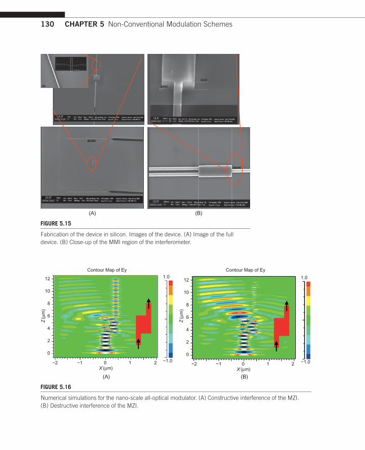
130 CHAPTER 5 Non-Conventional Modulation Schemes
Contour Map of Ey
12
10
8
6
4
2
0
−2 −1 0X (µm)
1 2 −1.0
1.0Contour Map of Ey
12
10
8
6
4
2
0
−2 −1 0X (µm)
Z(µ
m)
Z(µ
m)
1 2 −1.0
1.0
(A) (B)
FIGURE 5.16
Numerical simulations for the nano-scale all-optical modulator. (A) Constructive interference of the MZI. (B) Destructive interference of the MZI.
(A) (B)
FIGURE 5.15
Fabrication of the device in silicon. Images of the device. (A) Image of the full device. (B) Close-up of the MMI region of the interferometer.

131
view of one of the two beam splitters of the interferometer device. As mentioned, the overall length of this device is about 9 microns. Although this is small enough, the presented design concept can be applied for smaller devices as well. Figure 5.16 shows numerical simulations for the same MZI having dimensions of less than one square micron. Figure 5.16A shows the constructive interference state of the MZI and Figure 5.16B shows its destructive interference state. The difference between the constructive and the destructive conditions was obtained by adding spatially non-uniform absorption, which broke the balance between the two interfering beams within the MZI. The wavelength that was used in the simulation was 1.55 m. The waveguide was fabricated in silicon.
Note that the device presented in Figure 5.16 is a multi-mode interference (MMI) device, i.e. in the region of interference the waveguide is wider and the single-mode condition is no longer fulfilled. The interference between the multiple spatial modes is responsible for having the destructive output.
When the balance is broken, the interference between the multiple modes is such that energy is obtained at the device output. At the output of the MMI device, we go back into the single-mode waveguide and therefore some energy is back-reflected. The MMI is also wavelength-dependent, but this dependence is not as strong as resonators with high finesse.
Figure 5.17 shows results of an experimental characterization of the fabricated device. The figure shows measurements of the spectral response of the fabricated device, under illumination from above by a speckle pattern at 532 nm. One can see that the interferometer has a transmission peak (construc-tive interference) at approximately 1546 nm. The device is wavelength-dependent due to the MMI
5.2 All-Optical Plasma Dispersion Effect-Based Approach
1500 1520 1540 1560 1580 1600 1620 16400
0.5
1
1.5
2
2.5
3
3.5
Wavelength [nm]
Nor
mal
ized
out
put p
ower
Control light ONControl light OFF
FIGURE 5.17
Measurements of the spectral response of the fabricated device while illuminated by speckles at 532 nm.

132 CHAPTER 5 Non-Conventional Modulation Schemes
0 0.2 0.4 0.6 0.8 1 1.2 1.4 1.6
�10−3
0
0.2
0.4
0.6
0.8
1
1.2
1.4
1.6
Time [Sec]
Vol
t
Laser response
D.C 5%D.C 10%D.C 15%D.C 20%D.C 25%
(B)
(A)
0 50 100 150 200 250 300 350 400 450 500–3.5
–3
–2.5
–2
–1.5
–1
–0.5
0
0.5
1
1.5
Time [µsec]
Pow
er C
hang
e (%
)
Temporal response vs. wavelength
1540 nm1543 nm1548 nm1550 nm1555 nm1556 nm1564.5 nm
FIGURE 5.18
(A) Measurements of the temporal response of the device. The visible illumination was at 532 nm with pulses with a duty cycle of 5%. The various grey levels designate information wavelengths. (B) The temporal response of the visible modulation laser for various duty cycles (designated as D.C. at the right part of the figure).

133
structure and the substrate refractive index. However, the bandwidth is still as wide as 10 nm (while for instance with a resonator having a free spectral range of 100 nm and a finesse of 1000, the width is less than 0.1 nm).
Note that the spectral response does not change significantly after application of the illumination, which indicates that indeed the relevant effect occurring due to the external illumination is related to misbalanced absorption rather than to significant variation of the relative phase between two interfer-ing optical paths (which would have caused a shift in the spectral chart).
Figure 5.18A shows the measured temporal response of the device. It shows that a response rate above 1 MHz is indeed feasible. The visible illumination applied to the device was at 532 nm with pulses with duty cycle of 5%. The various lines designate the wavelength of the information. One may see that following the results of Figure 5.17, at a wavelength in which the interferometer pro-duces output (constructive interference as shown in Fig. 5.18A at 1543 nm), the illumination causes an attenuation of the output IR information signal. At a wavelength where no constructive interfer-ence exists, such as 1556 nm, one sees that the control light breaks the balance between the two arms expected to create destructive interference and therefore the output signal is high (when the illumina-tion is ON). Another reason for the high energy output at a destructive interference wavelength is due to scattering and back-coupling of the visible light to the detector. Note that this indicates that the real attenuation caused by the illumination (the “control” command) is even stronger, since it also over-comes the back-coupling of the scattered light.
Note that 1 MHz is not the true limit for the operation rate, because the true response rate was not measured due to equipment limitations. The limit of 1 MHz was imposed by the maximal spectral content obtained using the modulation rate of the available visible laser, rather than the true limit for the operation rate of the device itself. In Figure 5.18B one sees the measure of the pulses that the vis-ible laser can produce when being modulated at various duty cycles. One sees that those pulses can-not go below the microsecond limit even for a duty cycle of 5%.
Figure 5.19 shows the difference between the case of illumination with visible light (at 532 nm and a duty cycle of 5%) over the waveguide core versus direct illumination over the interferometer. One sees that illumination over the interferometer device produces about 2.5 times stronger contrast in comparison with direct illumination over the waveguide itself. This result emphasizes one of the advantages of this concept that uses an interferometer rather than just a simple waveguide.
Figure 5.20 shows a mapping of the power required in order to activate the all-optical modulator. The figure shows the measurements of the effect of the visible illumination power on the contrast of the modulation of the IR information beam (at 1546 nm). The current supplied to the visible 532 nm Nd:YAG laser is given in mA; 400 mA is the minimum current required to obtain the modulation effect.
Figure 5.21 shows the required optical power of the illumination laser in units of actual optical power rather than in units of current supplied to the laser driver. As seen from the chart, the minimal activating average power for the presented experimental setting (e.g. the power of the coupled light) is 0.2 mW. Note that this measurement was done using a visible laser operated at a frequency of 400 Hz with a duty cycle of 5%. Therefore, the average power in the continuous case will be 4 mW. The laser illuminated a spot area of more than 2000 m2. When the illumination is concentrated on an area of the nano-scale device having dimensions of less than 1 m2 (e.g. spot of 0.5 × 0.5 m2) the required power for this setting will be 500 nW.
5.2 All-Optical Plasma Dispersion Effect-Based Approach

134 CHAPTER 5 Non-Conventional Modulation Schemes
0 50 100 150 200 250 300 350 400 450 5000.965
0.97
0.975
0.98
0.985
0.99
0.995
1
1.005
Time [µsec]
Nor
mal
ized
pow
er
Waveguide / interferometer illumination effect
Waveguide illuminatedDevice illuminated
FIGURE 5.19
Measurements of the difference between the case of illumination (with visible light at wavelength of 532 nm and duty cycle of 5%) over a waveguide edge in comparison with illumination directly over the interferometer.
0 50 100 150 200 250 300 350 400 450 500–6
–5
–4
–3
–2
–1
0
Time [µsec]
Abs
orpt
ion
(%)
Illumination power effect
1298 [mA]
662 [mA]
1009 [mA]
528 [mA]
808 [mA]
400 [mA]
FIGURE 5.20
Measurements of the effect of visible illumination power on the contrast of the modulation of the IR information beam (at 1546 nm). The current supplied to the visible Nd:YAG laser is in mA; 400 mA is the minimal current required to obtain the modulation effect in the experimental setting.

135
Figure 5.22 presents a picture of the silicon device illuminated from above with a green laser while IR light is being coupled into it. The pic-ture also shows the projected speckle pattern that eventually generates the spatial non-uni-formity responsible for the discussed operation principle.
Note that although the described device is a modulator realized in a planar waveguide, a sim-ilar approach may be realized in fiber form. For instance, following the approach described in Ref. [16], silicon wires can be inserted into pho-tonic crystal fibers as well as regular fibers.
Figure 5.23 shows a fabrication attempt for such devices. Figure 5.23A shows a cross-sec-tion of a photonic crystal fiber with a silicon rod. Figure 5.23B shows the cross-section of a regu-lar fiber with a silicon core. Figure 5.23C shows
a side view of the fiber of Figure 5.23B showing the continuity of the silicon rod. In both Figures 5.23A and 5.23B, light was coupled to the silicon rods.
0 0.5 1 1.5 2 2.50
1
2
3
4
5
6
Illumination power [mW]
Abs
orpt
ion
(%)
FIGURE 5.21
The optical power of the visible modulating laser required to modulate the IR radiation passing through the optical waveguide.
5.2 All-Optical Plasma Dispersion Effect-Based Approach
Illumination from above
The device
Coupling light to device 1 µm
Projected specklepattern
FIGURE 5.22
The device illuminated from above while light is being coupled into it. In the right part one may see the projected speckle pattern responsible for the modulation due to the spatial non-uniformity.

136 CHAPTER 5 Non-Conventional Modulation Schemes
5.3 PARTICLE TRAPPING-BAsED MODULATION5.3.1 IntroductionThere is a recent need for a modulator that will allow a direct communication between the electronic computers and the optical links of communication. Furthermore, the internal on-board metal connec-tions existing today are facing their physical boundaries while an optical on-board communication may allow faster modulation rates [17]. Integration between the standard microelectronics, based on silicon CMOS technology, and micro-scale optical devices is a necessary condition for a high-speed optical on-board communication. In order to realize an electro-optical modulator on silicon chip, one has to overcome the weak electro-optical interaction in silicon. As previously presented, some have dealt with this issue by producing very long structures [8], others have made short devices using ring resonators [62], which have a high finesse and narrow spectral response.
The devices described in this subsection do not use the inherent electro-optical properties of sili-con but rather are based upon an implantation of a nano gold particle to modulate or to sense light. Thus, they also exhibit nanoscale dimensions.
5.3.2 All-Optical Nanomodulator, sensor, Wavelength Converter, Logic Gate and Flip-FlopIn this subsection shift and control in the position of a gold nanoparticle by using a special type of optical tweezers realized by guiding and confining light in a nano-size void structure in which the nanoparticle is placed [18] is demonstrated. The nano-size void is positioned in an air gap between two MMI regions of silicon waveguide. This segment is the core module in all the devices proposed in this subsection. The two input light beams that are coupled from both sides of the MMI regions interfere with each other and generate standing waves. The relative phase between the two coupled beams hav-ing opposite direction of propagation is controllable and therefore also the position of the fringes of the generated standing waves. Evanescent tails coming from the guided standing waves are interfered in the void and allow control of the position of a metallic nanoparticle that is being trapped in the void.
2 µm wide Si wire
180 µm
(A)
Si rod
10 µm Si core
220 µm
(B)
Si rod
(C)
FIGURE 5.23
(A) Photonic crystal fiber with silicon rod. (B) Regular fiber with silicon core. (C) Side view of the fiber of (B) showing the continuity of the silicon rod.
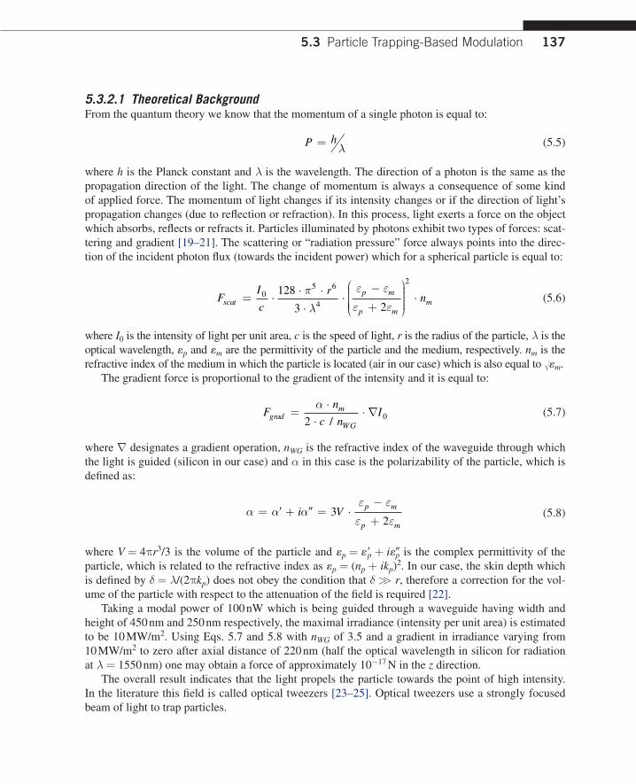
137
5.3.2.1 Theoretical BackgroundFrom the quantum theory we know that the momentum of a single photon is equal to:
P h=
(5.5)
where h is the Planck constant and is the wavelength. The direction of a photon is the same as the propagation direction of the light. The change of momentum is always a consequence of some kind of applied force. The momentum of light changes if its intensity changes or if the direction of light’s propagation changes (due to reflection or refraction). In this process, light exerts a force on the object which absorbs, reflects or refracts it. Particles illuminated by photons exhibit two types of forces: scat-tering and gradient [19–21]. The scattering or “radiation pressure” force always points into the direc-tion of the incident photon flux (towards the incident power) which for a spherical particle is equal to:
FI
c
rnscat
p m
p mm= ⋅
⋅ ⋅
⋅⋅
−
+
⋅0
5 6
4
2128
3 2
π
ε ε
ε ε
(5.6)
where I0 is the intensity of light per unit area, c is the speed of light, r is the radius of the particle, is the optical wavelength, p and m are the permittivity of the particle and the medium, respectively. nm is the refractive index of the medium in which the particle is located (air in our case) which is also equal to m.
The gradient force is proportional to the gradient of the intensity and it is equal to:
F
n
c nIgrad
m
WG
=⋅
⋅⋅ ∇
2 0/
(5.7)
where ∇ designates a gradient operation, nWG is the refractive index of the waveguide through which the light is guided (silicon in our case) and in this case is the polarizability of the particle, which is defined as:
ε ε
ε ε= + = ⋅
−
+ i V p m
p m
32
(5.8)
where V = 4r3/3 is the volume of the particle and p = p + ip is the complex permittivity of the particle, which is related to the refractive index as p = (np + ikp)
2. In our case, the skin depth which is defined by = /(2kp) does not obey the condition that >> r, therefore a correction for the vol-ume of the particle with respect to the attenuation of the field is required [22].
Taking a modal power of 100 nW which is being guided through a waveguide having width and height of 450 nm and 250 nm respectively, the maximal irradiance (intensity per unit area) is estimated to be 10 MW/m2. Using Eqs. 5.7 and 5.8 with nWG of 3.5 and a gradient in irradiance varying from 10 MW/m2 to zero after axial distance of 220 nm (half the optical wavelength in silicon for radiation at = 1550 nm) one may obtain a force of approximately 10−17 N in the z direction.
The overall result indicates that the light propels the particle towards the point of high intensity. In the literature this field is called optical tweezers [23–25]. Optical tweezers use a strongly focused beam of light to trap particles.
5.3 Particle Trapping-Based Modulation

138 CHAPTER 5 Non-Conventional Modulation Schemes
5.3.2.2 Fabrication of DevicesThe fabrication of submicron resolution pattern on silicon wafers while preserving improved aspect ratio is not a simple task but it is required for the realization of the proposed device. The high aspect ratio is required because of the structure of the nanometric void as well as in order to have efficient coupling of light from input optical fiber to the silicon waveguides.
The problem that we aim to address here is that the maximal aspect ratio of conventional electron resists (used for plasma etching) limits the obtainable spatial resolution. In the etching process both the electron resist mask as well as the silicon surface are being etched together. But conventional elec-tron resists are not stable in the plasma and therefore a thick electron resist layer is needed. This limits the resultant transversal resolution that may be realized. Below a novel approach allowing construc-tion of devices with increased obtainable resolution is presented. The proposed technique includes the following steps (it is schematically described in Fig. 5.24):
l Deposition of very thin layer (e.g. 50 nm) of electron resist on top of silicon on insulator (SOI) wafer (Fig. 5.24A).
l E-beam writing on the electron resist layer (schematically described by Fig. 5.24B).l Developing the electron resist layer (schematically described by Fig. 5.24B).
(A) (B)
(C) (D)
(E) (F)
FIGURE 5.24
(A) SOI wafer with deposited electron resist. (B) After e-beam writing and developing. (C) After metal deposition. (D) After lift-off process. (E) After plasma etching. (F) After metal removal.

139
l Metal deposition by sputtering process (e.g. about 20–30 nm in its thickness). See Figure 5.24C.l Lift-off of the electron resist layer together with the deposited metal (Fig. 5.24D).l Plasma etching process (schematically described by Fig. 5.24E).l Metal removal process (schematically described by Fig. 5.24F).
In Figure 5.25A and 5.25B the fabrication of the discussed device is presented. The fabrication is done using the process described in Figure 5.24. The two MMI regions as well as a slit between them are enlarged in Figure 5.25B. The particle is trapped in this slit. The device has two inputs of light from both sides of the MMI regions.
As previously mentioned the relative phase between the two inputs to the MMI regions deter-mines the position of the interference fringes which trap the nanoparticle. Figure 5.25C presents this in a numerical simulation. On the right side of Figure 5.25C one may see how indeed the control of the relative phase between the two inputs (the two inputs can also be generated by inputting light only from one side and using the back reflections from the edge of the device as the second input) shifts the intensity peaks of the standing waves. The numerical simulations of Figure 5.25C were performed using OptiFDTD which is a well-known and a proven software that solves the partial wave equa-tion via the finite element method. In the simulation we used the 2-D, TM mode and wavelength of 1.55 m for the input light signal.
Particles that are trapped by those intensity peaks will be shifted together with them. Because we are dealing with standing waves the generated gradient is relatively large (see Eq. 5.7) and therefore also the forces applied on the trapped particle.
5.3.2.3 Devices and Simulation ResultsThe basic configuration for the modulator, sensor, logic gate as well as flip-flop devices is presented in Figure 5.26. Two inputs control the position of the gold nanoparticle. This nanoparticle scatters the reference beam or transmits it to the output waveguide. This is an all-optical modulation operation where input light affects the amplitude of another input light.
In the case of a sensor application the output channel is the photonic output of the sensor which provides photonic readout corresponding to the phase difference between the two input channels to which one should couple the external light that it aims to sense. Since the sensing principle is not based upon absorption of photons, a multispectral infra-red sensor may be realized on a silicon chip since a wide range of different wavelengths will be coupled to the MMI-based device and control the position of the particle. A single wave-length reference at a different and preferable wavelength will be sensed according to the position of the nanoparticle.
Similarly in the case of a wavelength converter we may use 1 as the wavelength for the input channels and 2 as the wavelength of the reference beam. That way the input chan-nels containing information carried over optical carrier of 1
5.3 Particle Trapping-Based Modulation
Light input 1
Light input 2Interferometer Narrow slit
1 µm
(B)
(A)
(C)
FIGURE 5.25
(A, B) The fabricated device. (C) Numerical simulation for the generation of controllable standing waves in the slit between two MMI regions where the particle is being trapped.
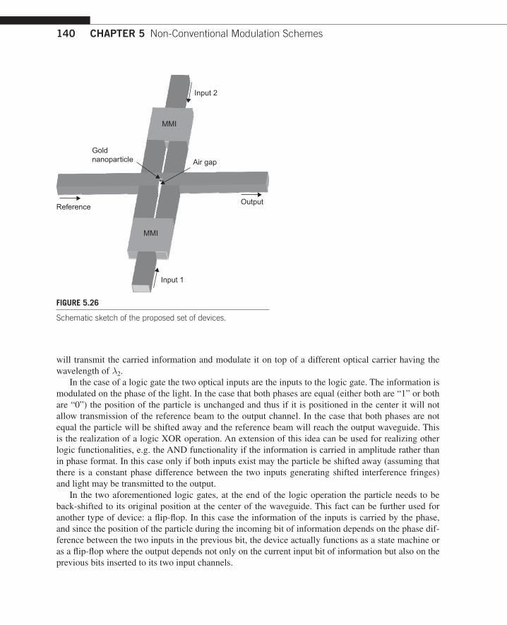
140 CHAPTER 5 Non-Conventional Modulation Schemes
will transmit the carried information and modulate it on top of a different optical carrier having the wavelength of 2.
In the case of a logic gate the two optical inputs are the inputs to the logic gate. The information is modulated on the phase of the light. In the case that both phases are equal (either both are “1” or both are “0”) the position of the particle is unchanged and thus if it is positioned in the center it will not allow transmission of the reference beam to the output channel. In the case that both phases are not equal the particle will be shifted away and the reference beam will reach the output waveguide. This is the realization of a logic XOR operation. An extension of this idea can be used for realizing other logic functionalities, e.g. the AND functionality if the information is carried in amplitude rather than in phase format. In this case only if both inputs exist may the particle be shifted away (assuming that there is a constant phase difference between the two inputs generating shifted interference fringes) and light may be transmitted to the output.
In the two aforementioned logic gates, at the end of the logic operation the particle needs to be back-shifted to its original position at the center of the waveguide. This fact can be further used for another type of device: a flip-flop. In this case the information of the inputs is carried by the phase, and since the position of the particle during the incoming bit of information depends on the phase dif-ference between the two inputs in the previous bit, the device actually functions as a state machine or as a flip-flop where the output depends not only on the current input bit of information but also on the previous bits inserted to its two input channels.
Input 2
Input 1
Reference
Air gap
MMI
MMI
Output
Goldnanoparticle
FIGURE 5.26
Schematic sketch of the proposed set of devices.

141
Note that in the logic gate application in order to allow cascading ability one needs to match the modulation formats of the two inputs with the format of the output channel. Thus, when the input information is using a phase format for the information while the output is an amplitude format, proper conversion must be performed. One simple way of doing such a conversion is by using an interferometer. One input to such an interferometer will be the output of the device and the other input will be a reference beam. The output of the interferometer will be phase information that corresponds to the input amplitude information [67].
In order to numerically demonstrate the photonic concept of modulation, the software “COMSOL Multiphysics” was used.
As previously mentioned, the conceptual sketch of the device is seen in Figure 5.26. A hole of air of 80 nm × 265 nm is being produced inside the reference waveguide between the two MMI regions. On the left side we have the reference beam that propagates along the waveguide and is coupled to the output of the device. On the upper and lower part we have the two photonic inputs that control the position of the gold nanoparticle inside the air gap.
In the numerical simulation an electromagnetic wave at wavelength of 1.55 m is excited and propagates along the reference waveguide until it approaches the output of the device. All silicon waveguides in Figure 5.26 consist of a channel waveguide with dimensions of 450 nm width and 250 nm height. In the simulation a gold nanoparticle (conductivity of = 3 × 10⁷ S/m) with diameter of 80 nm was used.
It was demonstrated that changing the position of the gold nanoparticle inside the air gap can drastically modify the output power flow. Figure 5.27A presents the refractive index of the simu-lated device. Figure 5.27B presents the power flow distribution along the device including the air gap (when there is no nanoparticle). Figures 5.27C and 5.27D present the power flow distribution along the device while the gold nanoparticle is being placed in the lower and upper part of the air gap, respectively.
One may see that the output extinction ratio being obtained for the two positions of the nanoparti-cle is about 8 dB. The nanoparticle was shifted 265 nm between its two positions. Note that due to its nanometric dimensions as well as the small value of the required shift, relatively high response rates of above 1 GHz may be obtained [26].
5.3.2.4 Preliminary Experimental ValidationsThis subsection presents the experimental demonstration for the common core of the proposed set of devices. It is experimentally shown how two optical inputs can indeed shift the trapped nanoparticle.
Note that gold nanoparticles have found broad applications in nanomaterials and nanobiotechnol-ogy [27]. In optical trapping studies, gold nanoparticles have been investigated as superior handles relative to polystyrene (PS) beads because of gold’s high polarizability which could lead to higher trap efficiency [28]. Such a large polarizability also offers the crucial added benefit of enhanced detection. The trapping forces on gold nanoparticles in the Rayleigh regime (diameter << wavelength) are significantly larger than on latex beads of similar size.
In this experiment unconjugated colloidal gold particles, which are produced with a very tight size distribution, were used. The nanoparticles are in a water solution and the overall net charge on the colloidal particle surfaces is negative. In order to connect these particles to the surface, an organic layer was used. It is called poly-L-lysine which is positively charged and thus acts as an adhesive
5.3 Particle Trapping-Based Modulation

142 CHAPTER 5 Non-Conventional Modulation Schemes
layer. First, poly-L-lysine was deposited on the SOI wafer which is electrostatically connected to the surface and after drying the residues, a few microliters of gold nanoparticles solution were dropped on it. The negative charge was electrically connected to the positive charge of the poly-L-lysine. This approach allowed very simple control of the particles’ density.
A 30-nm-diameter particle was experimentally implanted in the void. Experimentally the particle was shifted using an atomic force microscope (AFM) tip until it fell into the designated void. The procedure of pushing the particle with the tip is seen in Figure 5.28. The pushed particle is marked in the figure with a white arrow. The steps are numbered in the figure. In the last step (step #5) when the particle is already inside the void, we added in the right side of the image a 3-D chart of the particle as it was measured by the AFM.
Then, the particle was trapped by one of the high-intensity evanescent fringes while by changing the relative phase between the two inputs to the chip one could experimentally modify the
1.5 3
0.7
0.6
0.5
0.4
0.3
0.2
0.1
0.7
0.6
0.5
0.4
0.3
0.2
0.1
0.7
0.6
0.5
0.4
0.3
0.2
0.1
2.5
2
1.5
1Min: 1.00
Max: 3.48
Max: 0.750 Max: 0.744
Max: 0.747
1
0.5
0
0µm ×10−6
×10−6×10−6
×10−6 ×10−6
µm µm
Surface: Refractive indexSurface: Power flow, time
average, norm [W/m2]
Surface: Power flow, timeaverage, norm [W/m2]
Surface: Power flow, timeaverage, norm [W/m2]
0.5 1 1.5 2 2.5 3 3.5 4
Min: 3.355e−180
µm ×10−6
0.5
(A) (B)
(C) (D)
1 1.5 2 2.5 3 3.5 4Min: 5.676e−18
0µm ×10−6
0.5 1 1.5 2 2.5 3 3.5 4
Min: 2.098e−50
µm ×10−6
0.5 1 1.5 2 2.5 3 3.5 4
−0.5
−1
1.5
1
0.5
0µm
−0.5
−1
1.5
1
0.5
0
µm
−0.5
−1
1.5
1
0.5
0
−0.5
−1
FIGURE 5.27
Numerical simulations. (A) Scheme of the refractive index of the simulated device. (B) Power flow distribution along the device including the air gap. (C, D) The power flow distributions along the device while the gold nanoparticle ( = 3 × 10⁷ S/m) is placed in the lower and upper parts of 265 nm long air gap, respectively.

143
location of the fringes and the position of the particle (similarly to what occurs with optical tweezers). It was demonstrated that power of approximately only 100 nW inside the waveguide was sufficient to shift the particle to the other side of the trapping void (the void tunnel has length of about 1 m) as presented in Figure 5.29, where one may see the position of the trapped particle before and after the coupling of light to the device. Since light is capable of moving the particle, the proposed device can be used as an all-optical nanomodulator or as the core module for sensor, wavelength converter, logic gate or a flip-flop.
5.3 Particle Trapping-Based Modulation
2 1
34
5
Void
500 nm
FIGURE 5.28
Pushing the nanoparticle into the designated void using an AFM tip.
Before After
FIGURE 5.29
Experimentally obtained images. Before and after coupling light to the device.
144 CHAPTER 5 Non-Conventional Modulation Schemes
5.3.3 Electro-Optical ModulatorHere the operation principle is based on a design of a capacitor. A single-mode silicon waveguide is leading the wave into an SiO2 wider region; a nano air hole has been produced inside the SiO2 and two gold contacts are placed at each side of the capacitor to enable electrical field within the SiO2 region; finally a charged nano gold particle is displaced within the air gap by the electric field gener-ated in the capacitor [26].
When one couples light from an external light source like a tapered fiber carrying a 1.55 micron signal into the single-mode silicon waveguide, the output energy is strongly correlated to the position of the gold particle inside the air gap. When external voltage is applied on the capacitor’s contacts, the inner electrical field is attracting or repelling the charged nano gold particle. When the gold parti-cle is placed inside the optical path, most of the energy is being scattered and absorbed by the highly conductive particle and therefore the output energy is substantially decreased.
5.3.3.1 SimulationsTo verify the assumption and to design an efficient electro-optical modulator COMSOL Multiphysics was used to solve the partial wave equations for the proposed device:
∇× ∇×( ) − −( ) =− ε εr z r zE j k E1
0 02 0/
(5.9)
where r is the relative magnetic permeability, Ez is the transverse z component of the electric field, r is the dielectric coefficient, is the conductivity, is the angular frequency of the propagated light, k0 = 2/0 with 0 being the wavelength and 0 is a constant which is the permittivity of free space. In the simulations 2D, TM mode was used with 1.55 microns as the wavelength of the input signal.
Figure 5.30 illustrates the power distribution along the device from the input single-mode (SM) silicon waveguide, through the modulator and to the output waveguide. The figure presents the abso-lute value of the Poynting vector with the input power normalized to 1. Figure 5.30A shows the distri-bution when the nano gold particle is positioned at the lower part of the air gap. It clearly appears that the overlap between the optical mode and the nano gold particle is low, therefore most of the signal is not affected by the particle while the power passes input to output with low losses.
However, the dots appearing in the figure are related to the standing wave that is generated from the back reflection due to the large differences in the refraction indices between silicon (3.48) and SiO2 (1.45) with the presence of a conductive gold particle ( = 3 × 10⁷). This difference in refrac-tion indices also changes the period of the wave. From the standing wave one can extract that the SWR (standing wave ratio) is 1.25 which implies a reflection coefficient of 11%. The metallic con-tacts are separated from the silicon waveguide by a 200-nm layer of SiO2. The silica layer prevents the discharging of the gold particle as well as reduces losses introduced by skin effect/overlap between the optical mode and the highly conductive metallic electrodes.
Figure 5.30B shows the power distribution when the charged nano gold particle is displaced to the upper part of the air gap. Since the overlap between the optical mode and the particle is high, most of the energy is scattered, absorbed and reflected and the output power is substantially reduced. The standing wave in the input waveguide shows an SWR of 4.4 and a reflection coefficient of 63%.

145
Figures 5.30C and 5.30D present the cross-section of the power at the middle of the waveguide and through the modulator. The periodic signal at the input silicon waveguide is generated due to the reflection that causes the standing wave. One can see the change in reflection when the particle is manipulated to the higher part of the air gap. The output power demonstrates an expected modulation depth of 6 dB. When one integrates over the Poynting vector along the whole structure with/without the presence of the gold particle it is easily seen that losses of 0.82 dB are introduced by the nanoparti-cle. The metallic contacts in this specific design (of specific width and length for the silica layer) actu-ally introduce gain of the output energy with respect to a non-reflective/absorptive material. Due to the diffraction angle produced at the interface between the silicon and silica waveguide, the metallic
5.3 Particle Trapping-Based Modulation
8
1.62.42.2
21.81.61.41.2
10.80.60.40.2
1.4
1.2
1
0.8
0.6
0.4
0.2
00 0.1 0.2 0.3 0.4 0.5 0.6 0.7 0.8 0.9 1
6
4
2
0
−2
−4
−0.5 −0.3 −0.1 0.1 0.3 0.5 0.7 0.9 1.1 1.3−0.5 −0.3 −0.1 0.1 0.3 0.5 0.7
(A) (B)
(C) (D)
0.9 1.1 1.3
8
1.6
2
1.5
1
0.5
1.4
1.2
1
1.8
0.6
0.4
0.2
6
4
2
0
−2
−4
×10−6[m]
×10−5[m]0 0.1 0.2 0.3 0.4 0.5 0.6 0.7 0.8 0.9 1
×10−5[m]
×10−6[m]
×10−7[m] ×10−7[m]
Surface: abs(Hy_emwe*Ez) [W/m2)ab
s(H
y_em
we*
Ez)
[W/m
2 )
abs(
Hy_
emw
e*E
z) [W
/m2 )
Poynting vector, particle out Poynting vector, particle in
Surface: abs(Hy_emwe*Ez) [W/m2)
y
x
FIGURE 5.30
Numerical simulations. The Poynting vector distribution is presented in (A) and (B) when the nano gold particle is at the lower and upper part of the air gap, respectively. (A) shows a high transmission coefficient when the particle is set outside of the air gap and a low overlap between the optical mode and the particle. (B) simulates the scatterings, back-reflections and absorption that substantially reduce the output energy when the particle is set within the optical path. (C) and (D) depict the Poynting vector cross-section along the waveguide and through the modulator. The output energy is almost 1 at the OFF mode and 0.3 at the ON mode.

146 CHAPTER 5 Non-Conventional Modulation Schemes
contacts which are almost perpendicular to the wave help in reflecting the energy back to the output waveguide rather than to absorb it.
The chip design that is presented in Figure 5.31A is engineered to enable an in-plane coupling for both the input and the output signals. Therefore a unique Si funnel that changes the refractive index gradually from 60 nm to 450 nm was designed [29]. A curved silicon waveguide is leading the single-mode radiation at a wavelength of 1.55 microns into the modulator located at the top of the arc (perpendicular to the input fiber to disable noises and direct coupling between the input and output). The conductive wires lead to the contact pads placed far from the device to enable flexibility and simplified probing capabilities. External micro-electro-probing will apply various voltages in order to manipulate the position of the gold particle.
HSQ box
Electricalcontacts
SiO2 buried layer
(B)
30 µm 58 nm
154 nm
82 nm
Air gap
Electricalcontacts
Si funnel waveguides
Au markers
450nm single
mode Siwaveguides
(A)HSQ resist masking layer
FIGURE 5.31
(A) The chip design introduces a funnel which is a silicon waveguide that is used as a coupler and a medium for mode matching between external tapered fiber and internal single silicon (SM) waveguides. The modulator is positioned at the top of the SM silicon waveguide arc. Large electrical contacts are placed to enable simple operation and connection of micro-electro probes. (B) SEM images of the fabricated device; enlarged images of the modulator and the Si funnel tip.
147
5.3.3.2 FabricationThe device previously described was fabricated on a 200 nm Si/2 m SiO2 SOI wafer by means of three aligned electron beam lithographic processes using a LEICA-VISTEC EBPG-5 100 KeV machine. Having defined the aligning markers using optical lithography followed by the deposition of 10 nm Ti/60 nm Au by thermal evaporation and lift-off, the first step in the patterning of the sin-gle-mode waveguides was accomplished. This has achieved writing the waveguide structures on a 150-nm-thick negative resist (Dow Corning FOX-12 HSQ resist, dose 1000 C/cm2 for the lower-resolution structures) which has been used as a masking layer for the subsequent silicon etching by means of chlorine-based 5-min reactive ion etching (RIE) process (Cl2 30 sccm, Ar 20 sccm, RF power 170 W, pressure 100 mTorr, self bias 140 V using an Oxford Plasmalab 80 machine).
For the second step, i.e. the realization of the insulating container box for the metal nanoparticle, the HSQ resist was used again which after exposure and development becomes similar to silica (SiOx, where x is between 1.5 and 2). The third step, which included the realization of the electrical con-tacts, has been obtained again by an aligned electron beam lithography on a 1-m-thick positive resist (micro-resist UVIII, dose 22 C/cm2) followed by the deposition of a 10 nm Ti/60 nm Au metallic bilayer by evaporation and lift-off. The details of the obtained device are presented in Figure 5.31B.
5.3.3.3 Experimental TestingIn order to position the nano gold particle in the air gap, the same steps as described in subsection 5.3.2.4 have been accomplished. Colloidal gold unconjugated particles, which are produced with a size distribution of 30 nm ± 3 nm, were used.
A non-feedback method of the AFM (atomic force microscope) was used to displace a single nan-oparticle from the SiO2 to the air gap. Figures 5.32A and 5.32B show a nano gold particle that is positioned right on the edge of the nano air gap a moment before it was pushed inside. A parallel approach to be used for a chip containing many such modulators can allow positioning plurality of particles in the gaps by a unique polymer that connects exclusively on the one hand to the gold parti-cle and on the other hand to a unique material. Following a process of lithography may allow removal of this material from the chip except from the air gap locations which eventually will yield a selective assignment of the particles only to the gaps in a parallel methodology.
By using micro-electro-probing, various voltages in the range of several volts were applied on the SiO2 capacitor to manipulate the position of the particle in the air gap by changing the inner electrical field.
The best results that were received for several devices were obtained for voltages around a 10 V DC input. Much lower voltages and time-dependent pulses are yet to be examined. In Figures 5.32C and 5.32D one may see the single nano gold particle that is located in the air gap before and right after applying the electric field.
Measured shift of at least 20 nm in the air gap was demonstrated. This shift allows modulating the light that goes right through the device. Since the modulation rate is determined by the required shift of the nanoparticle while this shift should be small (only a few tens of nanometers) and since the par-ticle has high mobility inside the air gap due to the contracting polymer, a high modulation rate and very low-power dissipation are expected from this approach.
The estimation of the modulation rate can be derived from the time it takes for a charged spheri-cal particle to pass a given distance between the capacitor’s plates due to the applied electrical
5.3 Particle Trapping-Based Modulation

148 CHAPTER 5 Non-Conventional Modulation Schemes
force. Assuming a simplified model in which the particle has zero initial velocity the time estima-tion is:
TL
a
Ldm
VQR
Ld
VV= = =
2 2 2
3 0 0
ε
(5.10)
where L is the length of the shift, a is the acceleration of the particle, d is the distance between the capacitor plates, m is the mass of the particle, V is the applied voltage on the capacitor electrodes, Q is the charge of the particle, R is the radius of the particle, is the mass density of the particle, V0 is the voltage at which the particle was charged and 0 = 8.85 × 10⁻¹² F/m. For a gold particle with R = 15 nm, = 19 300 kg/m3 and d = 150 nm, L = 30 nm, that was charged at V0 = 200 V while applying a voltage of V = 10 V on the capacitor, one obtains T = 0.85 ns.
Air hole
Particles
Before
After
(A)
(B)
(C)
(D)
1.6 µm 1.1 µm
1.00.8
0.70.6
0.40.3
1.41.2
1.00.8
0.60.4
0.2
9
0.80.7
0.60.4
0.30.1
1.61.4
1.21.0
0.80.6
0.40.2
300 nm 200 nm
100 nm
80 nm
80 nm425 nm
FIGURE 5.32
AFM images demonstrating a randomly scattered deposition of nano gold particles near the air gap (A and B) and a single gold particle which was shifted by 20 nm in the air gap due to inner electrical field that was applied by external voltage connected to the electrical contacts of the modulator (C and D).
149
5.3.4 Tunable Nanodevices Fabricated by Controlled Deposition of Gold Nanoparticles Via Focused Ion BeamManipulation of nanoparticles with dimensions starting from few tens and up to few hundreds of nanom-eters can be used for photonic sensing and modulation applications [26]. Therefore, a mass production process allowing the deposition of the nanoparticles is a prerequisite requirement for those devices.
Several methods have been employed to produce deposition of nanoparticles on a surface using the atomic force microscope (AFM) tip in order to apply pulses of voltage into an insulating films [30,31], printing technique that uses electrostatic force to pattern PMMA (polymethyl methacrylate) [32], electrostatic force generated by p–n junction [33] and lithography process that uses conductive flexible poly-dimethyl-siloxane (PDMS) stamp to create charged substrates [34]. Another common method uses poly-L-lysine (PLL) which is a positive organic layer in order to coat the substrate and make an intermediary between the negative nanoparticles and the substrate. The linking between the surface and the poly-L-lysine as well as between the poly-L-lysine and the nanoparticles is based upon electrostatic bonding.
In this subsection we introduce a technique for significantly simplified deposition of charged nanoparticles at specific patterns based upon focused ion beam (FIB) technology. This technique is suitable for mass production fabrication and thus may allow large-scale realization of various nano-photonic modulators such as those mentioned in Ref. [26]. The main advantages of this technology are by having both high speed and precision deposition. In this subsection we will also discuss the fabrication procedure as well as the preliminary experimental characterization of a tunable device using a trapped nanoparticle [35].
5.3.4.1 Patterning MethodThe desired patterns were created using FIB with a gallium ion source. Patterning is performed by accelerating concentrated gallium ions to a specific area on the chip, which etches off any exposed surface. Positive gallium ions will also be implanted into the top few nanometers of the surface and therefore will create the basis for bonding with the nanoparticles. This trapped positive charge attracts the gold nanoparticles which are negatively charged as part of their fabrication process.
Figure 5.33 presents a schematic sketch of the system in which the desired pattern is created (inset). The imaging resolution and therefore the deposition resolution are determined by the FIB’s sputter limited signal-to-noise ratio of about 6 nm.
The proposed method was experimentally successfully applied to silicon oxide wafers, but can be extended to any other insulated material.
5.3.4.2 Experimental ResultIn the experiments, an unconjugated gold colloidal in an aqueous suspension was used. The diameters of the particles that were used were 200 nm and 30 nm while the standard deviation of the size distri-bution was less than 10% of the average.
In Figure 5.34 a resolution pattern with different spaces between two adjacent squares is realized. The width of the squares is 3 m with depth of 0.5 m. This pattern was created with ion beam hav-ing the following parameters: magnification of 2500, beam current of 0.28 nA and a high voltage of 5 KV. Following the patterning, 30-nm gold nanoparticles were deposited for 30 minutes, rinsed with purified HPLC water, dried with nitrogen and finally imaged topographically by scanning electron
5.3 Particle Trapping-Based Modulation
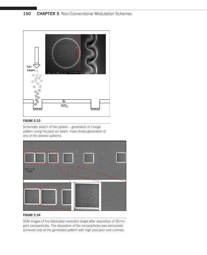
150 CHAPTER 5 Non-Conventional Modulation Schemes
FIGURE 5.33
Schematic sketch of the system – generation of charge pattern using focused ion beam. Inset shows generation of one of the desired patterns.
FIGURE 5.34
SEM images of the fabricated resolution target after deposition of 30-nm gold nanoparticles. The deposition of the nanoparticles was exclusively achieved only at the generated pattern with high precision and contrast.
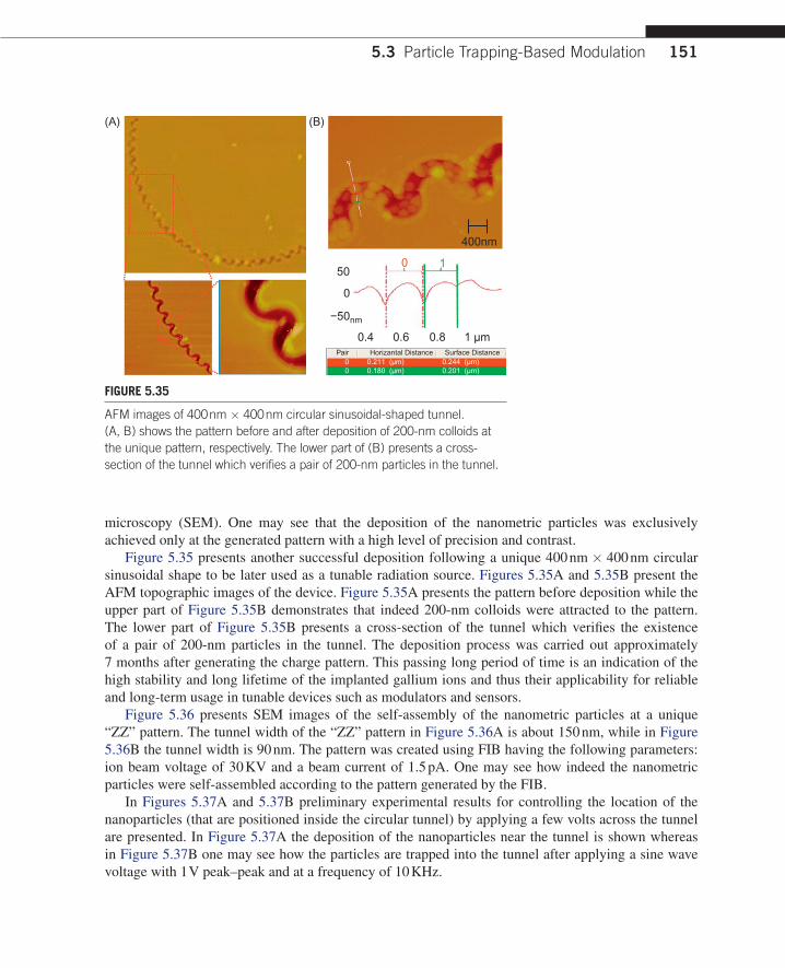
151
microscopy (SEM). One may see that the deposition of the nanometric particles was exclusively achieved only at the generated pattern with a high level of precision and contrast.
Figure 5.35 presents another successful deposition following a unique 400 nm × 400 nm circular sinusoidal shape to be later used as a tunable radiation source. Figures 5.35A and 5.35B present the AFM topographic images of the device. Figure 5.35A presents the pattern before deposition while the upper part of Figure 5.35B demonstrates that indeed 200-nm colloids were attracted to the pattern. The lower part of Figure 5.35B presents a cross-section of the tunnel which verifies the existence of a pair of 200-nm particles in the tunnel. The deposition process was carried out approximately 7 months after generating the charge pattern. This passing long period of time is an indication of the high stability and long lifetime of the implanted gallium ions and thus their applicability for reliable and long-term usage in tunable devices such as modulators and sensors.
Figure 5.36 presents SEM images of the self-assembly of the nanometric particles at a unique “ZZ” pattern. The tunnel width of the “ZZ” pattern in Figure 5.36A is about 150 nm, while in Figure 5.36B the tunnel width is 90 nm. The pattern was created using FIB having the following parameters: ion beam voltage of 30 KV and a beam current of 1.5 pA. One may see how indeed the nanometric particles were self-assembled according to the pattern generated by the FIB.
In Figures 5.37A and 5.37B preliminary experimental results for controlling the location of the nanoparticles (that are positioned inside the circular tunnel) by applying a few volts across the tunnel are presented. In Figure 5.37A the deposition of the nanoparticles near the tunnel is shown whereas in Figure 5.37B one may see how the particles are trapped into the tunnel after applying a sine wave voltage with 1 V peak–peak and at a frequency of 10 KHz.
5.3 Particle Trapping-Based Modulation
50
0.4 0.6
400nm
(A) (B)
0 1
0.8 1 µm
−50nm
0
0.211 (µm) 0.244 (µm)0Pair Horizantal Distance Surface Distance
0.180 (µm) 0.201 (µm)0
FIGURE 5.35
AFM images of 400 nm × 400 nm circular sinusoidal-shaped tunnel. (A, B) shows the pattern before and after deposition of 200-nm colloids at the unique pattern, respectively. The lower part of (B) presents a cross-section of the tunnel which verifies a pair of 200-nm particles in the tunnel.
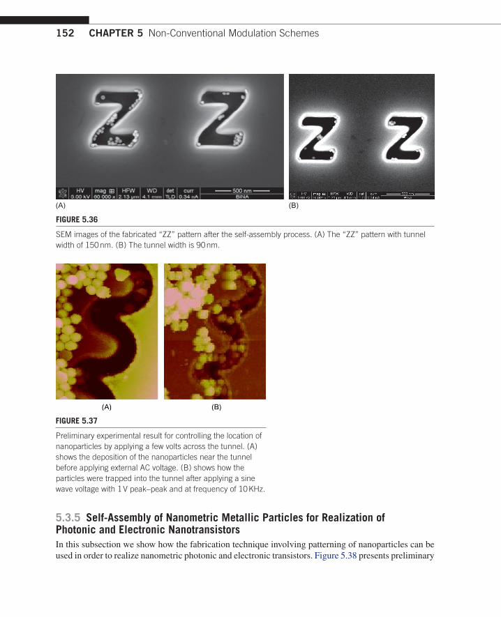
152 CHAPTER 5 Non-Conventional Modulation Schemes
5.3.5 self-Assembly of Nanometric Metallic Particles for Realization of Photonic and Electronic NanotransistorsIn this subsection we show how the fabrication technique involving patterning of nanoparticles can be used in order to realize nanometric photonic and electronic transistors. Figure 5.38 presents preliminary
(A) (B)
FIGURE 5.36
SEM images of the fabricated “ZZ” pattern after the self-assembly process. (A) The “ZZ” pattern with tunnel width of 150 nm. (B) The tunnel width is 90 nm.
FIGURE 5.37
Preliminary experimental result for controlling the location of nanoparticles by applying a few volts across the tunnel. (A) shows the deposition of the nanoparticles near the tunnel before applying external AC voltage. (B) shows how the particles were trapped into the tunnel after applying a sine wave voltage with 1 V peak–peak and at frequency of 10 KHz.
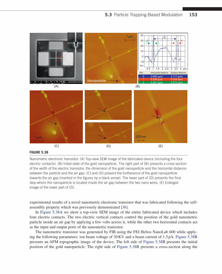
153
experimental results of a novel nanometric electronic transistor that was fabricated following the self-assembly property which was previously demonstrated [36].
In Figure 5.38A we show a top-view SEM image of the entire fabricated device which includes four electric contacts. The two electric vertical contacts control the position of the gold nanometric particle inside an air gap by applying a few volts across it, while the other two horizontal contacts act as the input and output ports of the nanometric transistor.
The nanometric transistor was generated by FIB using the FEI Helios NanoLab 600 while apply-ing the following parameters: ion beam voltage of 30 KV and a beam current of 1.5 pA. Figure 5.38B presents an AFM topographic image of the device. The left side of Figure 5.38B presents the initial position of the gold nanoparticle. The right side of Figure 5.38B presents a cross-section along the
5.3 Particle Trapping-Based Modulation
Nanoparticle
1 µm
1 µm
(A)
(C) (D) (E)
(B)
200 nm
40
30
20
10
0
–10
nm
Pair Horizontal distance Surface distance
0.5
0 2.695 (µm) 2.717 (µm)1 0.205 (µm) 0.219 (µm)2 0.257 (µm) 0.273 (µm)
1 1.5 2 2.5 3 3.5 4 µm
20
1
FIGURE 5.38
Nanometric electronic transistor. (A) Top-view SEM image of the fabricated device (including the four electric contacts). (B) Initial state of the gold nanoparticle. The right part of (B) presents a cross-section of the width of the electric transistor, the dimension of the gold nanoparticle and the horizontal distance between the particle and the air gap. (C) and (D) present the furtherance of the gold nanoparticle towards the air gap (marked in the figures by a black arrow). The lower part of (D) presents the final step where the nanoparticle is located inside the air gap between the two nano wires. (E) Enlarged image of the lower part of (D).

154 CHAPTER 5 Non-Conventional Modulation Schemes
width of the electronic transistor (denoted in the figure as pair #2) as well as verifying that indeed a 200-nm particle was positioned in an initial position with proper proximity to the air gap (denoted in the figure as pair #1). The horizontal distance between the initial state of the nanoparticle and the air gap was 2.695 m and it is denoted in the figure as pair #0.
The AFM tip was used in order to locate the gold nanoparticle inside the designated air gap. The furtherance of the gold nanoparticle toward the air gap was carried out using the mechanical “Nano manipulation” mode having the following parameters: x–y velocity of 0.1 m/s, z velocity of 10 nm/s and the z distance was selected to be –220 nm. The procedure of pushing the nanoparticle into the air gap is seen in Figures 5.38C and 5.38D. Figure 5.38E presents an enlarged image of the lower part of Figure 5.38D, where the gold nanoparticle is already located inside the air gap. The position of the gold nanoparticle is denoted in the figure by a black arrow.
The AFM measurements and imaging were carried out using the Nanoscope V Multimode scan-ning probe microscope. All images were obtained using the tapping mode with a single LTSP silicon probe (force constant of 48 N/m, Digital Instruments). The resonance frequency of this cantilever was approximately 167 kHz while the scan angle was maintained at 0°. The images were captured in the retrace direction with a scan rate of 0.5 Hz. The image resolution is 256 samples/line. After obtaining the measurements, the “planefit” and “flatting” functions were applied to each image of the sample. The dimensions of the particles were determined by an analysis of the phase and height of the extracted AFM images that were collected simultaneously using the Nanoscope Software Version 7.3.
In order to verify the assumption that indeed the nanoparticle was inserted into the air gap and that the proposed nanotransistor is functional, the R–V (resistance–voltage) curves for two possible cases were measured. The R–V curves were generated using the Agilent B1500A semiconductor device analyzer. The Y-axis on the left and right sides of Figure 5.39 presents the resistivity and the current flow of the device as a function of the voltage that was applied across the vertical pair of electrodes, respectively.
Figures 5.39A and 5.39B present the R–V curves where the gold nanoparticle is located outside and inside the air gap, respectively. One may see that when the particle is shifted and positioned inside the air gap between the two nanowires (by the two control electrodes) the current increases versus the applied voltage, i.e. the electric current is able to flow along the device. When the nano-particle is shifted away from the air gap (by applying the proper voltage across the control nanowire electrodes) the current remains zero, i.e. no current flow is measured through the device.
Note that in Figure 5.39 the R–V curve is presented by the left Y-axis. The I–V (current–voltage) plot is presented right Y-axis. The horizontal X-axis is the same for both plots.
Due to the self-assembly property of the nanoparticles that was previously demonstrated one may fabricate plurality of such nanotransistor devices in parallel on top of the same chip.
5.3.6 Design and Fabrication of 1X2 Nanophotonic switchIn this subsection we present the design and the fabrication of a 1X2 nanophotonic switch. The switch is a photonic T-junction in which a gold nanoparticle is being positioned in the junction using the tip of an atomic force microscope (AFM) [37].
The proposed 1X2 switch has the ability to control the direction of the wave that propagates along a photonic structure. The selectivity of the direction is determined by a gold nanoparticle having dimensions of a few tens of nanometers. This particle can be shifted. The shift of the gold nanoparticle can be

155
achieved by applying voltage or by illuminating it with a light source. The shift of the particle inside the air gap directs the input beam once to the left output of the junction and once to its right output.
Three types of simulations were used in order to realize the photonic T-junction and they are as follows: photonic crystal structures, waveguide made out of PMMA and a silicon waveguide.
5.3.6.1 Numerical SimulationsThe proposed device has a T-junction shape. In the 2-D simulations, TE “in-plane” mode analysis at a wavelength of 1.55 m was used. The electromagnetic wave is excited and propagates along the main waveguide until it approaches the 90 degrees “Y coupler”. A hole of air gap is being produced at the splitting point. The silicon waveguides consist of a channel waveguide with dimensions of 450 nm width and 250 nm height. Choosing the proper position of a nanoparticle in the junction can change the output channel through which the light is output. All simulations in this section were performed using two numerical softwares: R-Soft and COMSOL Multiphysics, which both solved the Maxwell equations for radiation propagation using Finite-Difference Time-Domain (FDTD) and Finite Element Method (FEM) approaches, respectively.
120K
00 200m
V1 (V) 100 m/div400m 600m 800m 1
1.5n
I1 (A)
100u/div2u
4u
6u
8u9u
R (
ohm
)
(B)
V1 (V) 100 m/div(A)
00
R (
ohm
)50
0M
/div
2G
4G
6G
7.9G
200m 400m 600m 800m
10m
0
I1 (A)
1
FIGURE 5.39
R–V curves of the device. (A) and (B) present the R–V curves of the nanometric device where the gold nanoparticle is being placed outside and inside the air gap, respectively.
5.3 Particle Trapping-Based Modulation
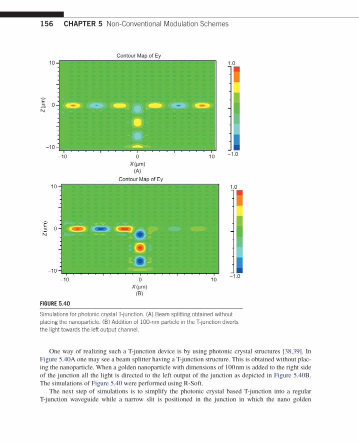
156 CHAPTER 5 Non-Conventional Modulation Schemes
One way of realizing such a T-junction device is by using photonic crystal structures [38,39]. In Figure 5.40A one may see a beam splitter having a T-junction structure. This is obtained without plac-ing the nanoparticle. When a golden nanoparticle with dimensions of 100 nm is added to the right side of the junction all the light is directed to the left output of the junction as depicted in Figure 5.40B. The simulations of Figure 5.40 were performed using R-Soft.
The next step of simulations is to simplify the photonic crystal based T-junction into a regular T-junction waveguide while a narrow slit is positioned in the junction in which the nano golden
Contour Map of Ey10
0
−10
−10 0X (µm)
Z(µ
m)
10−1.0
1.0
Contour Map of Ey10
0
−10
−10 0X (µm)
(A)
(B)
Z(µ
m)
10 −1.0
1.0
FIGURE 5.40
Simulations for photonic crystal T-junction. (A) Beam splitting obtained without placing the nanoparticle. (B) Addition of 100-nm particle in the T-junction diverts the light towards the left output channel.

157
particle ( = 3 × 10⁷ S/m) is placed. In Figure 5.41A one may see the simulation of such a device while the waveguide is made out of PMMA material (refraction index of about 1.6). The readout of the two outputs (the left and the right arms of the T-junction) versus the position of the nanoparticle is seen in Figure 5.41B. The size of the particle is 100 nm. The units of the horizontal axis of Figure 5.41B are in microns and thus one may see that shifting the particle a distance of about 400 nm switches the output from the left to the right arm of the T-junction device. One may see that an extinction
5.3 Particle Trapping-Based Modulation
X (µm)(A)
0
5
6
7
8
9
10
2 4 6 8 10
Z(µ
m)
–1.0
1.0
Particle position4.5
0.0
0.1
Mon
itor
outp
ut
0.2
4.6 4.7 4.8 4.9 5.0 5.1 5.2 5.3 5.4 5.5
(B)
FIGURE 5.41
Waveguide-based T junction. (A) Simulations for switching the output channel in a PMMA waveguide. (B) The same simulation as in (A) versus the position of the 100-nm particle.

158 CHAPTER 5 Non-Conventional Modulation Schemes
ratio of 1:17 (12 dB) may be obtained in the proposed device. The simulations of Figure 5.41 were performed using R-Soft.
The basic configuration of photonic structures (e.g. modulator, sensor and logic gate) is already based on silicon waveguide; therefore, in order to adapt the device for silicon a modification to the T-junction is made as depicted in Figure 5.42. The simulations in this part were carried out using COMSOL Multiphysics that solves the second-order partial differential wave equation (Eq. 6.9). The boundary condition at the input of the device was selected in such a way that the Poynting vector is equal to 1. The external boundary conditions were selected to be scattered (each one of them with a proper direction of scattering), while the internal boundary conditions were selected to be in “continuity”
−1
−2
−1
0
1
2
0 1 2 3 4 5 1
1.5
2
2.5
3
�10–6
�10–6
Min: 1.00
Min: 3.48Surface: Refractive index
(A)
−1 −0.5
3
2.5
2
1.5
1
0.5
0
−0.5
−1
−1.5
−2
−2.50 0.5 1 1.5 2 2.5 3 3.5 4 4.5 5 5.5
0.1
0.2
0.3
0.4
0.5
�10–6
�10–6
Min: 1549e–5
Min: 0.552Surface: Power flow, time average,norm (W/m2)
(B)
−1−0.5
3
2.5
2
1.5
1
0.5
0
−0.5
–1
−1.5
–2
−2.50 0.5 1 1.5 2 2.5 3 3.5 4 4.5 5 5.5
0.1
0.2
0.3
0.4
0.5
�10–6
�10–6
Min: 0.554Surface: Power flow, time average,norm (W/m2)
(C)−1−0.5
3
2.5
2
1.5
1
0.5
0
−0.5
–1
−1.5
−2
−2.50 0.5 1 1.5 2 2.5 3 3.5 4 4.5 5 5.5
0.1
0.2
0.3
0.4
0.5
�10–6
�10–6
Min: 5.406e–8
Min: 0.551Surface: Power flow, time average,norm (W/m2)
(D)Min: 3.639e–10
FIGURE 5.42
Numerical simulation. (A) Refractive index of the simulated device. (B) The power flow distribution along the “Y coupler” without the particle. (C and D) The power flow distribution along the “Y coupler” waveguide while the gold nanoparticle ( = 3 × 10⁷ S/m) is placed in the lower and upper part of the air gap, respectively.
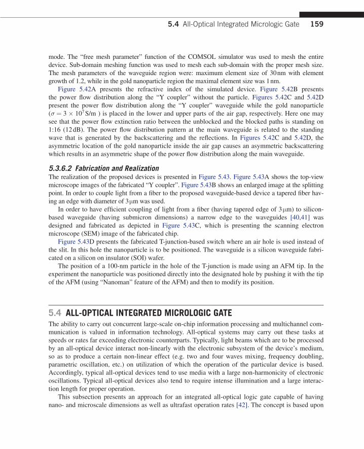
159
mode. The “free mesh parameter” function of the COMSOL simulator was used to mesh the entire device. Sub-domain meshing function was used to mesh each sub-domain with the proper mesh size. The mesh parameters of the waveguide region were: maximum element size of 30 nm with element growth of 1.2, while in the gold nanoparticle region the maximal element size was 1 nm.
Figure 5.42A presents the refractive index of the simulated device. Figure 5.42B presents the power flow distribution along the “Y coupler” without the particle. Figures 5.42C and 5.42D present the power flow distribution along the “Y coupler” waveguide while the gold nanoparticle ( = 3 × 10⁷ S/m ) is placed in the lower and upper parts of the air gap, respectively. Here one may see that the power flow extinction ratio between the unblocked and the blocked paths is standing on 1:16 (12 dB). The power flow distribution pattern at the main waveguide is related to the standing wave that is generated by the backscattering and the reflections. In Figures 5.42C and 5.42D, the asymmetric location of the gold nanoparticle inside the air gap causes an asymmetric backscattering which results in an asymmetric shape of the power flow distribution along the main waveguide.
5.3.6.2 Fabrication and RealizationThe realization of the proposed devices is presented in Figure 5.43. Figure 5.43A shows the top-view microscope images of the fabricated “Y coupler”. Figure 5.43B shows an enlarged image at the splitting point. In order to couple light from a fiber to the proposed waveguide-based device a tapered fiber hav-ing an edge with diameter of 3 m was used.
In order to have efficient coupling of light from a fiber (having tapered edge of 3 m) to silicon- based waveguide (having submicron dimensions) a narrow edge to the waveguides [40,41] was designed and fabricated as depicted in Figure 5.43C, which is presenting the scanning electron microscope (SEM) image of the fabricated chip.
Figure 5.43D presents the fabricated T-junction-based switch where an air hole is used instead of the slit. In this hole the nanoparticle is to be positioned. The waveguide is a silicon waveguide fabri-cated on a silicon on insulator (SOI) wafer.
The position of a 100-nm particle in the hole of the T-junction is made using an AFM tip. In the experiment the nanoparticle was positioned directly into the designated hole by pushing it with the tip of the AFM (using “Nanoman” feature of the AFM) and then to modify its position.
5.4 ALL-OPTICAL INTEGRATED MICROLOGIC GATEThe ability to carry out concurrent large-scale on-chip information processing and multichannel com-munication is valued in information technology. All-optical systems may carry out these tasks at speeds or rates far exceeding electronic counterparts. Typically, light beams which are to be processed by an all-optical device interact non-linearly with the electronic subsystem of the device’s medium, so as to produce a certain non-linear effect (e.g. two and four waves mixing, frequency doubling, parametric oscillation, etc.) on utilization of which the operation of the particular device is based. Accordingly, typical all-optical devices tend to use media with a large non-harmonicity of electronic oscillations. Typical all-optical devices also tend to require intense illumination and a large interac-tion length for proper operation.
This subsection presents an approach for an integrated all-optical logic gate capable of having nano- and microscale dimensions as well as ultrafast operation rates [42]. The concept is based upon
5.4 All-Optical Integrated Micrologic Gate

160 CHAPTER 5 Non-Conventional Modulation Schemes
stimulated emission in pumped gain medium [43]. The technique utilizes the dependence of a signal propagating through a stimulated emission medium (herein called gain medium) on the gain. This dependence is typically non-linear with respect to the gain. The idea is that an input signal controls the gain of the medium since the gain depends on the number of photons in the medium. Increasing the number of photons reduces the gain. The reference beam is passing through the gain medium and
(A) (B)
(C)
(E)
(D)
FIGURE 5.43
Fabricated “Y coupler”. (A) Top-view microscopic image of the overall fabricated device. (B) Enlarged image shows the input waveguide which splits into a pair of waveguides. (C and D) SEM images of the lower and upper encompass areas (shown in B) that define the coupling of light from fiber to the silicon waveguide and the fabrication of the T-junction itself, respectively. (E) Placing the particle in the slit (the particle is marked with a white arrow). The left part is an upper view of the particle and the right part is the 3-D mesh.

161
is coupled to the output of the device. Since the amplification of the medium is directly proportional to the logic inputs, a Boolean logic operation may be realized at the output of the device. Because a stimulated emission is involved the response rate of the operation mechanism is very short (an imme-diate response).
5.4.1 Operation PrincipleThe schematic sketch (see Fig. 5.44) for the basic all-optical logic gate contains a gain medium which is pumped continuously from the external source (not present in Fig. 5.44). The gain medium described in Figure 5.44 is quantum dots (QD) where the fabrication process of the proposed chip is described in Section 5.4.2. Note however that any gain medium can be used instead of QD. The refer-ence beam is a continuously present beam. Output wave = Reference × G, where G is the gain factor of the gain medium. There are also two input signals to the logic gate. Those signals are used as the control signal for the gain medium. If the control signal exists, the gain factor G is suppressed and the output beam exiting the gain module is equal to zero. Only in the case when both of the control signals are zero (Input1 and Input2 are both “0”) will one have an amplified output beam coming from the output of the medium. This is a logical function “NOR”.
Mathematically the gain of a gain medium depends on the energy passing through it (in our case the pumping is always on) as follows:
=+
0
1I
Isat
(5.11)
5.4 All-Optical Integrated Micrologic Gate
100 µm
Gain medium QD waveguide
Reference signalOutput
Input 2Input 1
2µm
FIGURE 5.44
Microscope image of the fabricated nanophotonic device. On the upper left corner one may see the SEM image of the fabricated QD waveguide.

162 CHAPTER 5 Non-Conventional Modulation Schemes
where is the gain per unit length [overall gain G = exp(L) where L is the length of the gain medium], I is the energy in the gain medium and Isat is the saturation energy level. From this equation it is simple to see that increasing the energy in the gain medium I correspondingly reduces the overall gain.
The operation rate of the all-optical gate is very fast since, as seen in the rate equations for the amplification medium (see Eqs. 5.12 and 5.13), the stimulated emission is a very fast process and basically depends only on the pumping power and the intensity developed in the medium and not only on the spontaneous relaxation times:
d
d
N
tR
NN N Wp
2 2
22 1= − − −
( ) ( )
(5.12)
where N2 and N1 are the populations of the two levels between which the amplification is generated, Rp is the rate of pumping to the upper energetic level, 2 is the relaxation time related to the spontane-ous processes, and W is related to the stimulated emission process which is proportional to the inten-sity that is developed inside the medium:
W G I( ) ( )
=
3
(5.13)
where is a constant, is the frequency, G is the gain spectral response and I is the intensity in the gain medium.
5.4.2 FabricationThe realization of an integrated all-optical circuit based upon gain medium can be obtained for instance by constructing optical waveguides in quantum dots (QD) photoresist [44,45]. The gain material is constantly pumped and thus, following the rate equations of a gain medium, input signals passing through the medium at wavelength corresponding to the gain/absorption spectral characteris-tics will evoke immediate stimulated emission.
The microscope image of fabricated photonic chip following the above-specified description may be seen in Figure 5.44 (SEM image of the edge of the waveguide is seen in the upper left corner). The waveguide is made out of QD where on the left side one may see two logic inputs and on the right the reference beam is input. This reference is coupled to the right side of the chip where the output detec-tor is located. The inputs affect the gain of the gain medium which controls the level of the reference beam that is going to the output. This yields, as previously explained, optical logic NOR gate.
The integrated chip option for realizing the proposed approach may include realization of the gain medium by fabricating ZrO2 film (that was used as photo-resist) doped with CdSe@ZnS QDs which have a significant gain factor [44,45] over small interaction length. This fabrication process was applied to generate the chip seen in Figure 5.44.
The X-ray diffraction (XRD) spectra of QD-doped zirconia thin films at different annealing temperatures are seen in Figure 5.45. A clear transition from amorphous to partially crystalline is observed above 400°C.
Due to the low fill-factor of QDs in the sample (< 1% by volume) an effective medium model was not needed to account for the effect of the QD dispersion. Due to condensation of the matrix, a significant

163
increase in the refractive index of the film and a concordant decrease in thickness were consist-ently observed with increasing annealing temperature. For example, following heat treatment at only 100°C, the average film refractive index and thickness (thin film of ZrO2) was found to be 1.60 and 81 nm, while after annealing at 300°C these values changed to 1.75 and 39 nm.
5.4.3 Experimental TestingAlthough a chip was fabricated (Fig. 5.44), for the preliminary results of the experimental investiga-tion optical semiconductor amplifiers (OSA) [46,47] were used as the gain medium while the input signals are input through optical fibers. The bits of one of the input channels are delayed in com-parison to the other. The purpose of the delay is to generate relative shift of half the pulse in order to demonstrate that even if the pulses are superimposed one on top of the other and the overall ampli-tude is increased, the output of the proposed device remains the same (due to the saturation of the gain medium). This is one of the very important advantages gained by the proposed approach. In the experimental investigation the modulation rate was 15 MHz and the pulse width was 15 ns. As previ-ously mentioned the OSA gain medium was constantly pumped.
In Figure 5.46 one may see the measurements of input A, input B, both inputs together and the obtained output for that case respectively (going from the lower signal sequences presented in Fig. 5.46, upwards). From the results seen in Figure 5.46 one may conclude that only when both inputs A and B are zero is the output “1”, otherwise it is “0”. This is exactly the realization of the logic NOR gate operation. Note that the output channel as it is presented in Figure 5.46 and which was captured by the scope was deliberately shifted in the time axis, a shift of about 15 ns. This shift in the time axis was done in order to correct (or compensate) the temporal delay of about 15 ns (marked in the figure) that was generated due to the difference between the lengths of the cable that was used when connect-ing the input signals and the cable connecting the output of the device to the scope channels.
5.4 All-Optical Integrated Micrologic Gate
27
(101)0
50
100
150
200
(002) (110)
100D200D300D400D500D
30 33 36 392θ (°)
Sig
nal i
nten
sity
(re
lativ
e)
FIGURE 5.45
XRD spectra of QD-doped zirconia thin films at different annealing temperatures.
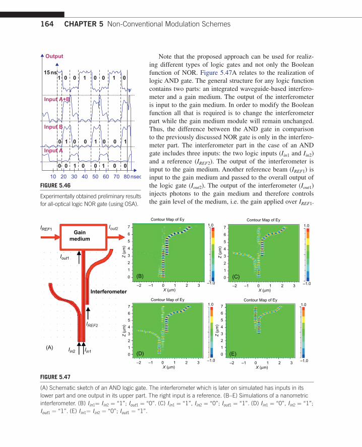
164 CHAPTER 5 Non-Conventional Modulation Schemes
Note that the proposed approach can be used for realiz-ing different types of logic gates and not only the Boolean function of NOR. Figure 5.47A relates to the realization of logic AND gate. The general structure for any logic function contains two parts: an integrated waveguide-based interfero-meter and a gain medium. The output of the interferometer is input to the gain medium. In order to modify the Boolean function all that is required is to change the interferometer part while the gain medium module will remain unchanged. Thus, the difference between the AND gate in comparison to the previously discussed NOR gate is only in the interfero-meter part. The interferometer part in the case of an AND gate includes three inputs: the two logic inputs (Iin1 and Iin2) and a reference (IREF2). The output of the interferometer is input to the gain medium. Another reference beam (IREF1) is input to the gain medium and passed to the overall output of the logic gate (Iout2). The output of the interferometer (Iout1) injects photons to the gain medium and therefore controls the gain level of the medium, i.e. the gain applied over IREF1.
15 ns
Input A+B
Output
Input B
Input A
0 0 1 0 0 1 0 0
10010010
1 0 0 1 0 0 1 0
10 20 30 40 50 60 70 80 nsec
FIGURE 5.46
Experimentally obtained preliminary results for all-optical logic NOR gate (using OSA).
Gainmedium
IREF1
Iout1
Iin1Iin2
Interferometer
(A)
Contour Map of Ey
7
6
5
4
3
2
1
0
–2 –1 0 1 2 3
Z (
µm)
X (µm)
(B)–1.0
1.0Contour Map of Ey
7
6
5
4
3
2
1
0
–2 –1 0 1 2 3
Z (
µm)
X (µm)
(C)–1.0
1.0
Contour Map of Ey
7
6
5
4
3
2
1
0
–2 –1 0 1 2 3
Z (
µm)
X (µm)
(D)–1.0
1.0Contour Map of Ey
7
6
5
4
3
2
1
0
–2 –1 0 1 2 3
Z (
µm)
X (µm)
(E)–1.0
1.0
Iout2
IREF2
FIGURE 5.47
(A) Schematic sketch of an AND logic gate. The interferometer which is later on simulated has inputs in its lower part and one output in its upper part. The right input is a reference. (B–E) Simulations of a nanometric interferometer. (B) Iin1= Iin2 = “1”; Iout1 = “0”. (C) Iin1 = “1”, Iin2 = “0”; Iout1 = “1”. (D) Iin1 = “0”, Iin2 = “1”; Iout1 = “1”. (E) Iin1= Iin2 = “0”; Iout1 = “1”.

165
This results in obtaining the desired output from the device for proper combinations of the two logic inputs to the gate.
Figures 5.47B–E present the simulations of the interferometer device. All simulations presented in this section were done using numerical software of R-Soft using a Finite Difference Time Domain (FDTD) numerical approach in order to solve Maxwell’s equations. As seen from the simulations, the interferom-eter is designed such that its output is equal to IREF2 −Iin1 − Iin2 (which is needed to obtain the AND func-tionality) while the energy of IREF2 is twice the energy of the two inputs such that only when both of them are present does the output of the interferometer become zero, which means that the output of the overall device (i.e. the output of the gain medium) is logic one (i.e. a functionality of logic AND gate).
5.5 POLARIzING AND sPECTRALLy sELECTIVE PHOTONIC DEVICE BAsED UPON DIELECTRIC NANORODsIntegrated photonic devices having polarizing or spectrally selective capabilities may be very applica-ble as part of a photonic chip to be used for optical communication applications where controlling and modifying the spectral [48,49] and especially the polarization state of light [50,51] plays a major role.
Nanostructures have been intensively studied in the last few decades due to their great potential and applicability for electronic and photonic devices. In recent years, ZnO nanostructures [52] have been of particular focus, because of their special properties. ZnO is an n-type semiconductor with a wide band-gap of 3.3 eV, a high refractive index of 2.3, optical transparency, electrical conductivity and piezo electricity [53]. The nanostructure has a diameter and length which can be much smaller than the wavelength of visible light. Such a configuration has useful optical, chemical and electrical properties while being non-toxic, inexpensive and chemically stable [54].
In this subsection we present a simple approach for fabricating dielectric ZnO nanorods having controllable dimensions, which can be easily adapted for mass production. An air slit can be used as an optical waveguide since the beam propagating in the slit will be bounced back from the nanorods surrounding the slit. The rods surrounding the slit act as an optical waveguide cladding, confining the light in the slit. The confined light is reflected with a known polarization as well as spectral selectiv-ity. The dimension of the nanorods surrounding the air gap waveguide determines the polarization and spectral properties of the light that remains guided. Thus, the main contribution described by this subsection is in introducing a novel approach for realizing on-chip photonic devices that can be used as a waveguide polarizer or spectral filter [55].
5.5.1 Fabrication ProcessThe ZnO nanorods were prepared on three different types of substrates: bare glass, fluorine-doped tin oxide (FTO) and indium tin oxide (ITO). The substrate was rinsed with deionized water, acetone and ethanol. Then a thin layer of ZnO was deposited on the substrate by radio frequency (RF) magnetron-sputtering. The sputtering condition consisted of 100 watt RF power and 15 mTorr pressure of argon for 10 minutes. After the sputtering, there was no change in the optical transparency of the substrate.
For subsequent growth of highly oriented ZnO nanorods the coated substrate was immersed in baths of two different concentrations. The baths consisted of a solution of 0.01 M zinc nitrate hexahy-drate Zn(NO3)2·6H2O (Sigma-Aldrich) and 0.4 M sodium hydroxide NaOH (Sigma-Aldrich) which
5.5 Polarizing and Spectrally Selective Photonic Device

166 CHAPTER 5 Non-Conventional Modulation Schemes
will be described as high concentration, or a solution of 0.001 M zinc nitrate Zn(NO3)2·6H2O and 0.01 M sodium hydroxide NaOH which is described as low concentration. In both cases the solvent was deionized water at 70°C [56].
During the deposition, the solution was stirred on a hot plate. The resulting films were rinsed with deionized water and then with ethanol for 10 minutes in a sonicator bath [57]. After each 60 minutes of deposition, the solution was replaced by a fresh one. The indication that showed the end of the reaction in a given solution was that the solution changed its color from transparent to white.
The chemical reactions in the creation of ZnO nanorods [58] are described in Eq. 5.14:
Zn OH Zn OH
Zn OH ZnO H O
ZnO H O ZnO s
+ − −
− −
−
+ →→ +
+ → +
24
2
42
22
2
22
2
2
2
( )
( )
( ) 22OH−
(5.14)
In the fabrication process, it was possible to control the dimensions of the nanorods by chang-ing the deposition time in the chemical bath. The results show that growth for 20–120 minutes in the chemical bath yields rods of 150–4200 nm in length with a diameter of 25–170 nm. In Table 5.1 one can see a summary of the various parameters used for the fabrication process and the resulting lengths and diameters of the nanorods.
The c-axis of sputtered ZnO crystals was preferentially oriented perpendicular to the substrate [59]. Figure 6.48A shows an X-ray diffraction (XRD) pattern of as-grown ZnO nanorods on bare glass. The intensities of the ZnO peak are very sharp, strong and between 2 = 34° and 35°, which corresponded to the (0 0 2) orientation of ZnO nanorods. Thus, one may conclude that high-quality hexagonal single-crystal ZnO nanorods are formed, and this is also shown by the inset SEM image in the right upper corner of Figure 5.48A. For comparison, the XRD measurement of ZnO nano powder is presented in Figure 5.48B.
For the characterization of the size, length and concentration of the obtained nanorods, a focused ion beam (FIB) FEI Helios 600 system was employed. High-resolution SEM (HR-SEM) cross- sectional images of ZnO nanorods which were obtained for different reaction times (20, 40, 60 min-utes growth in a low concentration and 60, 120, 180, 240 minutes at the high concentrations) are shown in Figure 5.49.
Table 5.1 Concentration of Zinc Ion and Hydroxide which are Required for Optimal Growth of the Nanorods
Zinc Ion (M) NaOH (M) Time Deposition (min) Length (nm) Diameter (nm)
0.001 0.1 20 150 25
0.001 0.1 40 250 50
0.001 0.1 60 500 65
0.01 0.4 30 600 50
0.01 0.4 60 1000 70
0.01 0.4 120 2500 120
0.01 0.4 180 3500 150
0.01 0.4 240 4200 170
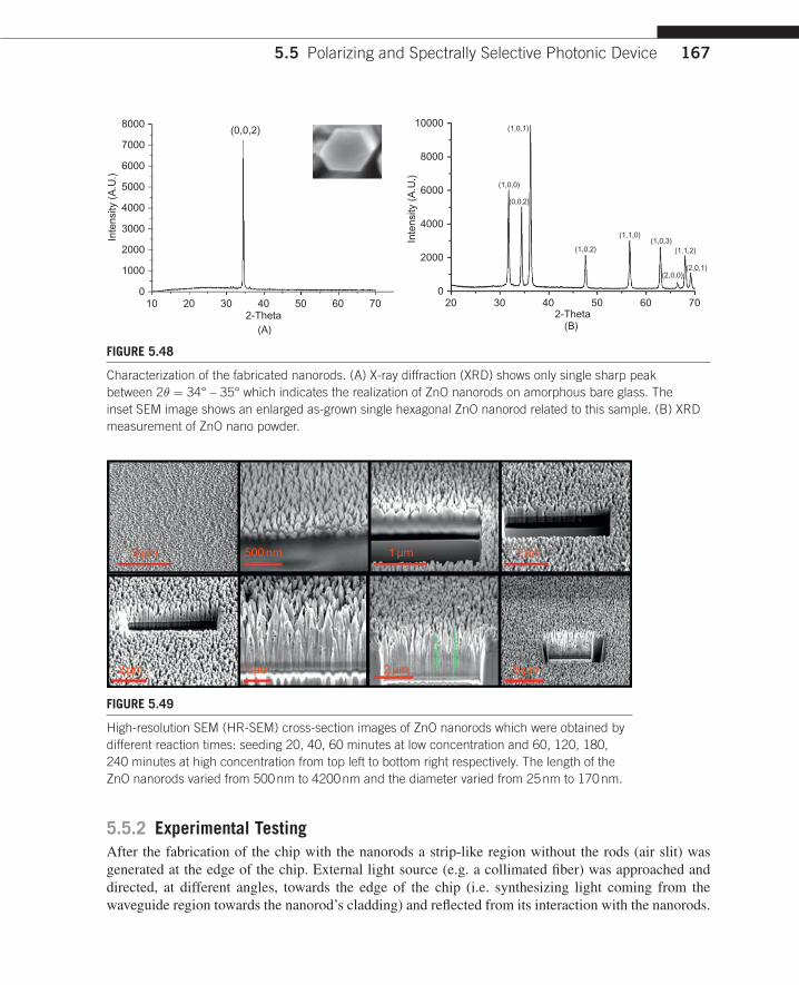
167
5.5.2 Experimental TestingAfter the fabrication of the chip with the nanorods a strip-like region without the rods (air slit) was generated at the edge of the chip. External light source (e.g. a collimated fiber) was approached and directed, at different angles, towards the edge of the chip (i.e. synthesizing light coming from the waveguide region towards the nanorod’s cladding) and reflected from its interaction with the nanorods.
5.5 Polarizing and Spectrally Selective Photonic Device
100
1000
2000
3000
4000
Inte
nsity
(A
.U.)
5000
6000
7000
8000(0,0,2)
(A) (B)
20 30 402-Theta 2-Theta
50 60 70 200
2000
4000
6000
Inte
nsity
(A
.U.)
8000
(1,0,1)
(1,0,0)
(0,0,2)
(1,0,2)
(1,1,0)(1,0,3)
(1,1,2)
(2,0,1)(2,0,0)
10000
30 40 50 60 70
FIGURE 5.48
Characterization of the fabricated nanorods. (A) X-ray diffraction (XRD) shows only single sharp peak between 2 = 34° – 35° which indicates the realization of ZnO nanorods on amorphous bare glass. The inset SEM image shows an enlarged as-grown single hexagonal ZnO nanorod related to this sample. (B) XRD measurement of ZnO nano powder.
3 µm 500 nm
2 µm 1 µm
1 µm
2 µm
2 µm
5 µm
FIGURE 5.49
High-resolution SEM (HR-SEM) cross-section images of ZnO nanorods which were obtained by different reaction times: seeding 20, 40, 60 minutes at low concentration and 60, 120, 180, 240 minutes at high concentration from top left to bottom right respectively. The length of the ZnO nanorods varied from 500 nm to 4200 nm and the diameter varied from 25 nm to 170 nm.
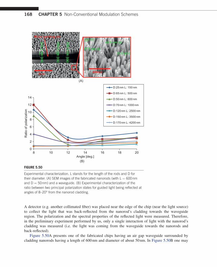
168 CHAPTER 5 Non-Conventional Modulation Schemes
A detector (e.g. another collimated fiber) was placed near the edge of the chip (near the light source) to collect the light that was back-reflected from the nanorod’s cladding towards the waveguide region. The polarization and the spectral properties of the reflected light were measured. Therefore, in the preliminary experiment performed by us, only a single interaction of light with the nanorod’s cladding was measured (i.e. the light was coming from the waveguide towards the nanorods and back-reflected).
Figure 5.50A presents one of the fabricated chips having an air gap waveguide surrounded by cladding nanorods having a length of 600 nm and diameter of about 50 nm. In Figure 5.50B one may
0
2
4
6
8
10
12
14
8 10 12 14 16 18 20
Rat
io o
f pol
ariz
atio
n
Angle [deg.]
D:25 nm L: 150 nm
D:65 nm L: 500 nm
D:50 nm L: 600 nm
D:70 nm L: 1000 nm
D:120 nm L: 2500 nm
D:150 nm L: 3500 nm
D:170 nm L: 4200 nm
2µm 400nm
Wave guiding slit
(B)
(A)
FIGURE 5.50
Experimental characterization. L stands for the length of the rods and D for their diameter. (A) SEM images of the fabricated nanorods (with L = 600 nm and D = 50 nm) and a waveguide. (B) Experimental characterization of the ratio between two principal polarization states for guided light being reflected at angles of 8–20° from the nanorod cladding.

169
see a summary of the polarization-selective properties of such a waveguide. The reflection measure-ments were performed by launching an incident linearly polarized light beam along the axis of the waveguide while slightly changing the incident angle. The measurements plotted in this figure are the ratio between the two principal reflected polarization states, obtained on various fabricated chips with nanorods having different dimensions, versus the reflection angle in degrees. Since the waveguides have a anumerical aperture of NA = 0.35, the relevant range of reflected angles is up to about 12 degrees and this also was the angular range for which the reflected light was measured. The exper-iment was performed with red light at a wavelength of 633 nm.
In Figure 5.51 the same measurements were repeated but this time using unpolarized white light incident on the waveguide from a collimated fiber source with a divergence less than 1 mrad. The reflected light was collected by a similarly collimated fiber and measured through a spectrometer. The measurement thus provides the spectral reflection curves of devices on chips having different nanorod parameters. The curves correspond to spectral measurements of reflected light for incident angle of 10 degrees. All values in Figure 5.51 are in arbitrary intensity units.
5.5.3 Preliminary Results and DiscussionIt was shown that waveguides surrounded by plane cladding nanorods exhibit polarization and spec-tral selectivity which is dependent on the physical dimensions of the nanorods. In order to obtain such selectivity one needs to fabricate nanorods having lengths below the optical wavelength since the selectivity is enhanced when the length is reduced. Therefore, fabricating a waveguide with cladding nanorods whose length is shorter than the wavelength can be used as a polarizer (as seen from Fig. 5.50). Following a numerical estimation, the propagation length inside the waveguides that is required to obtain a polarization ratio above 10 for all relevant angular ranges is only a few tens of microns.
5.5 Polarizing and Spectrally Selective Photonic Device
a) L:500 nm, D:65 nm
b) L:600 nm, D:50 nm
c) L:1000 nm, D:70 nm
d) L:2500 nm, D:120 nm
e) L:3500 nm, D:150 nm
f) L:4200 nm, D:170 nm
e
df
bc
a
3000
10
20
30
40
50
60
70
80
90
100
400 500 600Wavelength (nm)
Ref
lect
ion
(%)
700 800 900 1000
FIGURE 5.51
Experimental characterization of the spectral reflection curve, for angle of incident of 10 degrees, for chips with cladding nanorods having different dimensions. L stands for the length of the rods and D for their diameter.
170 CHAPTER 5 Non-Conventional Modulation Schemes
The spectral reflection was also shown to be dependent on the physical dimensions of the nano-rods. Especially visible in Figure 5.51 was the generated dip in spectral reflection at a wavelength of about 380 nm, for chips with rods having lengths below 1000 nm and diameter below 70 nm, or the peak at 500 nm that was significantly attenuated in the chip with rods having a length of 500 nm (diameter 65 nm). For the dip at a wavelength of 380 nm the reflection value was varied by a factor 6 and at the peak at wavelength of 500 nm the reflection value was varied by a factor of 9. Therefore such waveguides can also act as spectral filters.
The proposed structure was demonstrated as an in-plane waveguide. In order to also obtain vertical confinement of the guided light, the following fabrication procedure is proposed: first to coat a stripe of metallic layer on top of the chip. Then the nanorods will be grown everywhere on the chip except where the stripe is located (this will happen naturally by itself when applying the same growth procedure). This generated stripe will later become our waveguide. The generated metallic layer will be used as a mirror. Another chip having only the metallic layer (and no nanorods) will be placed on special verti-cal spacers on top of the first chip. Both chips will be aligned such that the two metallic layers will be one above the other. The nanorods will confine the light in its in-plane interaction while the mirrors will confine the light in the vertical axis. In the future one may use ZnO nanorods for surface enhanced spec-troscopies by coating their tips with metals as was done [60] with quantum dots and nanorods [61–67].
References [1] O. Limon, L. Businaro, Z. Zalevsky, Miniaturized Bragg modulator on a silicon chip, J. Nano Photonics 3
(2009) 031760. [2] S.M. Sze, Physics of Semiconductor Devices, John Wiley & Sons, New York, 1981 pp. 367–369. [3] D. Abraham, Z. Zalevsky, A. Chelly, J. Shappir, M. Rosenbluh, Silicon on insulator photo-activated modu-
lator, Microelectronics J. 39 (2008) 1429–1432. [4] D. Abraham, Z. Zalevsky, A. Chelly, J. Shappir, Fabrication of vertically positioned silicon on insulator
photo-activated modulator, PNFA 7 (2009) 190–197. [5] K. Biswas, S. Kal, Etch characteristics of KOH, TMAH and dual doped TMAH for bulk micromachining of
silicon, Microelectronics J. 37 (2006) 519–525. [6] A. Chelly, Y. Cohen, A. Sa’ar, J. Shappir, Pyramid-shaped silicon photodetector with subwavelength aper-
ture, IEEE Trans. Electron. Devices 49 (2002) 986–990. [7] S. Stepanov, S. Ruschin, Modulation of light by light in silicon-on-insulator waveguides, Appl. Phys. Lett.
83 (2003) 5151–5153. [8] H.K. Tsang, C.S Wong, T.K. Liang, I.E. Day, S.W. Roberts, A. Harpin, et al., Optical dispersion, two-photon
absorption and self-phase modulation in silicon waveguides at 1.5 m wavelength, Appl. Phys. Lett. 80 (2002) 416–418.
[9] M. Fetterman, C.P. Chao, S.R. Forrest, Fabrication and analysis of high-contrast InGaAsP–InP Mach–Zehnder modulation for use at 1.55 m wavelength, IEEE Photon. Technol. Lett. 8 (1996) 69–71.
[10] O. Leclerc, C. Duchet, P. Brindel, M. Goix, E. Grard, E. Maunand, et al., Polarisation-independent InP push–pull Mach–Zehnder modulation for 20 Gbit/s soliton regeneration, Electron. Lett. 34 (1998) 1011–1013.
[11] V. Van, T.A. Ibrahim, K. Ritter, P.P. Absil, F.G. Johnson, R. Grover, et al., All-optical nonlinear switching in GaAs–AlGaAs microring resonators, IEEE Photon. Technol. Lett. 14 (2002) 74–76.
[12] C.K. Tang, G.T. Reed, Highly efficient optical phase modulator in SOI waveguides, Electron. Lett. 31 (1995) 451–452.
171
[13] D. Marris-Morini, X. Le Roux, D. Pascal, L. Vivien, E. Cassan, J.M. Fedeli, et al., High speed all-silicon optical modulator, J. Lumin. 121 (2006) 387–390.
[14] D. Marris, E. Cassan, L. Vivien, Response time analysis of SiGeSi modulation-doped multiple-quantum-well structures for optical modulation, J. Appl. Phys. 96 (2004) 6109–6112.
[15] S.F. Preble, V.R. Almeida, M. Lipson, Optically controlled photonic crystal nanocavity in silicon, SPIE 49th Annual Meeting, Proceedings of SPIE vol. 5511 (2004) 10–17 .
[16] Z. Zalevsky, A.K. George, F. Luan, G. Bouwmans, P. Dainese, C. Cordeiro, et al., Photonic crystal in-fiber devices, Opt. Eng. 44 (2005) 125003.
[17] C. Luo, J.D. Joannopoulos, S. Fan, Nonlinear photonic crystal micro devices for optical integration, Opt. Lett. 28 (2003) 637–639.
[18] A. Shahmoon, Y. Abraham, O. Limon, L. Bitton, A. Frydman, Z. Zalevsky, All-optical nano modulator, sen-sor, wavelength converter, logic gate and flip flop based on manipulated gold nanoparticle, J. Nanophotonics (in print).
[19] L.N. Ng, B.J. Luff, M.N. Zervas, J.S. Wilkinson, Forces on a Rayleigh particle in the cover region of a pla-nar waveguide, J. Lightwave Technol. 18 (2000) 388–400.
[20] L.N. Ng, B.J. Luff, M.N. Zervas, J.S. Wilkinson, Propulsion of gold nanoparticles on optical waveguides, Opt. Commun. 208 (2002) 117–124.
[21] K.C. Neuman, S.M. Block, Optical trapping, Rev. Sci. Instrum. 75 (2004) 2787–2809. [22] K. Svoboda, S.M. Block, Optical trapping of metallic Rayleigh particles, Opt. Lett. 19 (1994) 930–932. [23] P.A. Maia Neto, H.M. Nussenzveig, Theory of optical tweezers, Europhys. Lett. 50 (2000) 702–708. [24] A. Casaburi, G. Pesce, P. Zemánek, A. Sasso, Two- and three-beam interferometric optical tweezers, Opt.
Commun. 251 (2005) 393–404. [25] A. Mazolli, P.A. Maia Neto, H.M. Nussenzveig, Theory of trapping forces in optical tweezers, Proc. R. Soc.
Lond. A 459 (2003) 3021–3041. [26] O. Limon, L. Businaro, A. Gerardinoc, L. Bittond, A. Frydmand, Z. Zalevsky, Fabrication of electro optical
nano modulator on silicon chip, Microelectron. Eng. 86 (2009) 1099–1102. [27] M.C. Daniel, D. Astruc, Gold nanoparticles: assembly, supramolecular chemistry, quantum-size-related
properties, and applications toward biology, catalysis, and nanotechnology, Chem. Rev. 104 (2003) 293–346.
[28] P.M. Hansen, V.K. Bhatia, N. Harrit, L. Oddershede, Expanding the optical trapping range of gold nanopar-ticles, Nano Lett. 5 (2005) 1937–1942.
[29] V.R. Almeida, R.R. Panepucci, M. Lipson, Nanotaper for compact mode conversion, Opt. Lett. 28 (2003) 1302–1304.
[30] P. Mesquida, A. Stemmer, Maskless nanofabrication using the electrostatic attachment of gold particles to electrically patterned surfaces, Microelectron. Eng. 61–62 (2002) 671–674.
[31] N. Naujoks, A. Stemmer, Localized functionalization of surfaces with molecules from solution using elec-trostatic attraction, Microelectron. Eng. 67–68 (2003) 736–741.
[32] H.O. Jacobs, S.A. Campbell, M.G. Steward, Approaching nanoxerography: The use of electrostatic forces to position nanoparticles with 100 nm scale resolution, Adv. Mater. 14 (2002) 1553–1557.
[33] D.H. Tsai, S.H. Kim, T.D. Corrigan, R.J. Phaneuf, M.R. Zachariah, Electrostatic-directed deposition of nanoparticles on a field generating substrate, Nanotechnology 16 (2005) 1856.
[34] M. Kang, H. Kim, B. Han, J. Suh, J. Park, M. Choi, Nanoparticle pattern deposition from gas phase onto charged flat surface, Microelectron. Eng. 71 (2004) 229–236.
[35] A. Shahmoon, O. Limon, O. Girshevitz, Y. Fleger, H.V. Demir, Z. Zalevsky, Tunable nano devices fabricated by controlled deposition of gold nanoparticles via focused ion beam, Microelectron. Eng. 87 (2010) 1363–1366.
[36] A. Shahmoon, O. Limon, O. Girshevitz, Z. Zalevsky, Self assembly of nano metric metallic particles for realization of photonic and electronic nano transistors, Int. J. Mol. Sci. 11 (2010) 2241–2252.
References
172 CHAPTER 5 Non-Conventional Modulation Schemes
[37] A. Shahmoon, M. Birenboim, A. Frydman, Z. Zalevsky, Design and fabrication of 1X2 nano photonic switch, J. Nanotechnology (2010) Article ID 953212.
[38] T.T. Alkeskjold, J. Lægsgaard, A. Bjarklev, D.S. Hermann, J. Anawati, J. Broeng, et al., All-optical modula-tion in dye-doped nematic liquid crystal photonic bandgap fibers, Opt. Exp. 12 (2004) 5857–5871.
[39] M.F. Yanik, S. Fan, M. Soljacic, J.D. Joannopoulos, All-optical transistor action with bistable switching in a photonic crystal cross-waveguide geometry, Opt. Lett. 28 (2003) 2506–2508.
[40] P.E. Barclay, K. Srinivasan, O. Painter, Design of photonic crystal waveguides for evanescent coupling to optical fiber tapers and integration with high-Q cavities, J. Opt. Soc. Am. B 20 (2003) 2274–2284.
[41] P.E. Barclay, K. Srinivasan, M. Borselli, O. Painter, Efficient input and output fiber coupling to a photonic crystal waveguide, Opt. Lett. 29 (2004) 697–699.
[42] A. Rudnitsky, M. Nathan, M. Nazarathi, B. Larom, A. Martucci, L. Businaro, et al., Micro scale photonic integrated all-optical logic gate. Proc. 35th Micro and Nano Engineering Conference (MNE), O-NANO-20 (September 2009).
[43] Z. Zalevsky, A. Rudnitsky, Devices and methods for optical signal control, Patent application #12/401, 779 (2007).
[44] J.J. Jasieniak, I. Fortunati, S. Gardin, R. Signorini, R. Bozio, A. Martucci, et al., Highly efficient amplified stimulated emission from CdSe–CdS–ZnS quantum dot doped waveguides with two-photon infrared optical pumping, Adv. Mater. 20 (2007) 69–73.
[45] J.J. Jasieniak, J. Pacifico, R. Signorini, A. Chiasera, M. Ferrari, A. Martucci, et al., Luminescence and amplified stimulated emission in CdSe–ZnS-nanocrystal-doped TiO2 and ZrO2 waveguides, Adv. Funct. Mater. 17 (2007) 1654–1662.
[46] Y. Kim, J.H. Kim, Y.M. Jeon, S. Lee, D.H. Woo, S.H. Kim, et al., All-optical flip-flop based on optical bistability in an integrated SOA/DFB-SOA, in: A. Sawchuk (Ed.), Optical Fiber Communications Conference (Vol. 70 of OSA Trends in Optics and Photonics), Optical Society of America (2002) paper TuF5.
[47] H. Ono, M. Yamada, M. Shimizu, S-Band EDFA with multistage configuration design, characterizations and gain tilt compensation, J. Lightwave Tech. 21 (2003) 2240–2247.
[48] M. Djavid, A. Ghaffari, M.S. Abrishamian, Coupled-mode analysis of photonic crystal add-drop filters based on ring resonators, J. Opt. Soc. Am. B 25 (2008) 1829–1832.
[49] Z. Wang, T. Sang, L. Wang, H. Jiao, Y. Wu, J. Zhu, et al., Narrowband multichannel filters and integrated optical filter arrays, Appl. Opt. 47 (2008) C1–C8.
[50] C.H. Chen, L. Pang, C.-H. Tsai, U. Levy, Y. Fainman, Compact and integrated TM-pass waveguide pola-rizer, Opt. Express 13 (2005) 5347–5352.
[51] T. Findaldy, B. Chen, D. Booher, Single-mode integrated-optical polarizers in LiNbO3 and glass wave-guides, Opt. Lett. 8 (1983) 641–643.
[52] R. Triboulet, The scope of the ZnO growth, Proc. SPIE 4412 (2001) 1–8. [53] G. Agarwal, R.F. Speyer, Current change method of reducing gas sensing using ZnO varistors,
J. Electrochem. Soc. 145 (1998) 2920–2925. [54] N. Beermann, L. Vayssieres, S.E. Lindquist, A. Hagfeldt, Photoelectrochemical studies of oriented nanorod
thin films of hematite, J. Electrochem. Soc. 147 (2000) 2456–2461. [55] S. Buhbut, A. Rudnitsky, M. Rosenbluh, A. Zaban, Z. Zalevsky, Polarizing and spectrally selective photonic
device based upon dielectric nanorods, Microelectron. Eng. 87 (2010) 1319–1322.[56] R.B. Peterson, C.L. Fields, B.A. Gregg, Epitaxial chemical deposition of ZnO nanocolumns from NaOH,
Langmuir 20 (2004) 5114–5118. [57] L. Vayssieres, K. Keis, S.E. Lindquist, A. Hagfeldt, Purpose-built anisotropic metal oxide material: 3D
highly oriented microrod array of ZnO, J. Phys. Chem. B 105 (2001) 3350–3352. [58] B. Liu, H.C. Zeng, Room temperature solution synthesis of mono-dispersed single-crystalline ZnO nano-
rods and derived hierarchical nanostructures, Langmuir 20 (2004) 4196–4204.
173
[59] B. Renee, C.L. Fields, B.A. Gregg, Epitaxial chemical deposition of ZnO nanocolumns from NaOH solu-tions, Langmuir 20 (2004) 5114–5118.
[60] T. Mokari, E. Rothenberg, I. Popov, R. Costi, U. Banin, Selective growth of metal tips onto semiconductor quantum rods and tetrapods, Science 18, 304 (2004) 1787–1790.
[61] S.E. Habas, P. Yang, T. Mokari, Selective growth of metal and binary metal tips on CdS nanorods, J. Am. Chem. Soc. 130 (2008) 3294–3295.
[62] V.R. Almeida, C.A. Barrios, R.R. Panepucci, M. Lipson, All-optical control of light on a silicon chip, Nature 431 (2004) 1081–1083.
[63] R.A. Soref, B.R. Bennett, Kramers-Kronig analysis of E-O switching in silicon, in: M.A. Mentzer, S. Sriram (Eds.), Integrated Optical Circuit Engineerng IV, Proc. SPIE 704 (1986) 32–37.
[64] Q. Xu, B. Schmidt, S. Pradhan, M. Lipson, Micrometre-scale silicon electro-optic modulator, Nature 435 (2005) 325–327.
[65] R.A. Soref, B.R. Bennett, Electro-optical effects in Silicon, IEEE J. Quantum. Electron. 23 (1987) 123–129.
[66] O. Limon, A. Rudnitsky, Z. Zalevsky, M. Nathan, L. Businaro, D. Cojoc, A. Gerardino, All-optical nano modulator on a silicon chip, Opt. Exp. 15 (2007) 9029–9039.
[67] Z. Zalevsky, A. Rudnitsky, M. Nathan, Nano photonic and ultra fast all-optical processing modules, Opt. Exp. 13 (2005) 10272–10284.
References
175Integrated Nanophotonic Devices. DOI:© 2010 Elsevier Inc. All rights reserved.
10.1016/B978-1-4377-7848-9.00006-92010
CHAPTER OUTLINE HEAD
6.1 Introduction ....................................................................................................................................1756.2 SPR Phenomena ..............................................................................................................................177
6.2.1 Propagating Surface Plasmons ................................................................................... 1776.2.1.1 Surface Plasmons at the Interface of Semi-Infinite Metal–Dielectric .........................1776.2.1.2 Effects of the Finite Metal Film Thickness ................................................................1816.2.1.3 The 2 × 2 Abeles Matrix Approach for the Optics of Multilayers ...............................1866.2.1.4 The Field Distribution Calculation ............................................................................188
6.2.2 Localized SPR .......................................................................................................... 1906.2.2.1 Absorption and Scattering by Metal Nanospheres ....................................................1906.2.2.2 Absorption and Scattering by Anisotropic Nanoparticles ..........................................1936.2.2.3 Field Enhancement and Surface-Enhanced Optical Effects ......................................1966.2.2.4 Enhanced Optical Transmission Through Nanoapertures in Metals ..........................200
6.3 Applications of Plasmonics ..............................................................................................................2056.3.1 Sensing ................................................................................................................... 205
6.3.1.1 Definitions Related to Optical Sensors .....................................................................2056.3.1.2 Evanescent Field Sensing .......................................................................................2066.3.1.3 Sensing with PSPR .................................................................................................2076.3.1.4 Recent Developments in PSPR Sensing ..................................................................2196.3.1.5 Sensing with LSPR and Nanostructure Design .........................................................2216.3.1.6 Surface-Enhanced Spectroscopies ..........................................................................2276.3.1.7 Sensing with EOT ....................................................................................................227
6.3.2 Light Concentration and Photovoltaics ........................................................................ 2316.4 Future Directions .............................................................................................................................232References ............................................................................................................................................233
Plasmonics 6CHAPTER
6.1 INTRODUCTIONA new field of research has emerged recently called “plasmonics” that deals with surface plasmon res-onance (SPR)-related science and technology. The objective of this chapter is to acquaint the reader with the principles of the SPR phenomenon and its applications, particularly in sensing. The SPR is a quantum electromagnetic (EM) phenomenon arising from the interaction of light with free elec-trons at a metal–dielectric interface emerging as a longitudinal EM wave in a two-dimensional gas of charged particles such as free electrons in metals. Under certain conditions the energy carried by the photons is transferred to collective excitations of free electrons, called surface plasmons (SPs), at that interface. This transfer of energy occurs only at a specific resonance wavelength of light when

176 CHAPTER 6 Plasmonics
the momentum of the photon matches that of the plasmon [1]. The SPs excited are strongly localized across the interface, and may be considered classically as EM surface waves that propagate along the interface and decay exponentially with distance normal to the interface. SPR is responsible for a dip in reflectance at the specific wavelength, the dip resulting from the absorption of optical energy in the metal. Since SP waves are tightly bound to metal–dielectric interfaces penetrating around 10 nm into the metal (the so-called skin depth) and typically more than 100 nm into the dielectric (depend-ing on the wavelength), they concentrate EM waves in a region that is considerably smaller than their wavelength, a feature that suggests the possibility of using SPs for the fabrication of nanoscale phot-onic circuits operating at optical frequencies [2]. This constitutes an important area of research, since surface-plasmon-based circuits are known to merge the fields of photonics and electronics at the nano-scale, thereby enabling them to overcome the existing difficulties related to the large size mismatch between the micrometer-scale bulky components of photonics and the nanometer-scale electronic chips.
There are two main types of SPs with respect to their propagation characteristics along the inter-face: extended or propagating and localized. The propagating SP is considered as more classical since it has been known for a longer time. However, the latest advancements in nanotechnology have made the fabrication of structures with nm-scale features feasible, thus the localized SPR has become a sub-ject of immense interest during the last two decades. Localized SPs are excited in metallic structures with lateral dimensions less than half the wavelength of the exciting EM wave. A third type of plas-mons may be mentioned called long-range SPR (LRSPR) which exists in thin metal films or stripes characterized by low attenuation and traveling along the surface for distances up to a few mm in the visible or even a few cm in the infrared. This latter type might have applications in active photonic components and highly sensitive sensors; however, the research on LRSPR is still in its early days.
In the case of propagating SPR (PSPR), plasmons propagate along the interface between metal and dielectric, for distances of the order of microns to tens and even hundreds of microns and decay evanescently in the z direction normal to the interface with 1/e decay length of the order of half the wavelength (~200 nm for wavelengths in the visible range). The interaction between the metal sur-face-confined EM waves and the molecular layer of interest leads to shifts in the plasmon resonance, which can be observed in three modes: (a) angle resolved, (b) wavelength shift, and (c) imaging. In the first two modes, one measures the reflectivity of light from the metal surface as a function of either wavelength (at constant incidence angle) or as a function of incidence angle (at constant wave-length). The third mode uses light of both constant wavelength and incidence angle to interrogate a two-dimensional region of the sample, mapping the reflectivity of the sample as a function of posi-tion. In each of these modes one can measure intensity, phase or polarization change.
For the case of localized SPR (LSPR), light interacts with particles much smaller than the inci-dent wavelength. This leads to a plasmon that oscillates locally around the nanoparticle with frequency known as the LSPR. Similar to PSPR, the LSPR is sensitive to changes in the local dielectric envi-ronment. Typically, researchers measure changes in the local dielectric environment through LSPR wavelength-shift measurements, although a variant of angle-resolved sensing for the LSPR is also pos-sible. Both PSPR and LSPR can provide thermodynamic and real-time kinetic data for binding proc-esses. Moreover, although PSPR spectroscopy provides much higher sensitivity to changes in the bulk refractive index than LSPR spectroscopy, the response of the two techniques becomes compa-rable when measuring short-range (in the nm vicinity of the metal surface) changes in the refractive index owing to a molecular adsorption layer. This is a result of the much smaller sensing volume offered by the LSPR sensors, as the EM-decay length is 40–50 times shorter than that of the PSPR sensors.

177
Moreover, advances in synthetic and lithographic fabrication techniques allow researchers to tune the localized resonance wavelength through the visible, near infrared, and into the infrared regions of the EM spectrum, by varying shape, size, and material of the nanoparticles that support the LSPR. This offers additional flexibility when designing LSPR sensing experiments.
The PSPR biosensors have been widely applied in a diverse range of fields, including molecu-lar recognition and disease immunoassays, etc. Even though conventional SPR biosensors are more sensitive than other label-free devices, they are still unable to achieve the direct detection of small molecular (few hundreds of daltons) interactions or low molecular concentrations (physiological concentration) on the surface of the biosensor. Consequently, various proposals have been devel-oped to enhance the sensitivity or resolution of biosensors by using different SPR modes or detec-tion methods. Also, various LSPR biosensors have been proposed which employ the strong UV–Vis absorption band of the metal nanoparticles to yield an area mass detection limit of 100–1000 pg/mm2. However, this detection capability is poorer than that of conventional PSPR biosensors by an order of at least 100 times. On the other hand the local EM field enhancement near nanostructures causes huge enhancement of other spectroscopic signals such as surface-enhanced Raman scattering (SERS) and surface-enhanced fluorescence (SEF). These spectroscopic techniques provide another important sensing parameter which is specificity. The enhancement factor depends strongly on the shape of the nanostructure and the type of the metal.
6.2 SPR PHENOmENA6.2.1 Propagating Surface PlasmonsPropagating SP waves are excited with TM-polarized EM waves when the component of the k-vector
along the metal–dielectric interface matches the SP k-vector. The con-dition of TM polarization is needed to generate the charge distribution on the metal–dielectric interface. In the mentioned case the electric field has a component perpendicular to the interface. The SP phe-nomenon can easily be understood, and its main characteristics can be determined by solving Maxwell’s equation to the boundary-value problem. We start our discussion by considering SPs on the interface of semi-infinite metal and dielectric then the effect of the finite thick-ness of the metal film will be considered.
6.2.1.1 Surface Plasmons at the Interface of Semi-Infinite Metal–DielectricConsidering the geometry in Figure 6.1, that consists of two semi-infinite media with dielectric constants εm, εs representing metal on dielectric substrate. By assuming TM plane and harmonic electromag-netic fields in the metal and the substrate with the appropriate waves:
E r t E E
H r t H
j xj zjk z i k x t
j yjk
zj xj, ( , , )
, ( , , )
| | ( )( ) =( ) =
− −
−
0
0 0
e e
e
zzj xjz i k x t| | ( )e −
(6.1)
x
z
metal ε m
dielectric sample ε s
++ +++ +++− − − − − − −−
y
FIgURE 6.1
Metallic thin film and dielectric layer with nm m= ε and ns s= ε complex refractive indices respectively, and separated by the z axis, supporting SPW at the interface in the metal side.
6.2 SPR Phenomena

178 CHAPTER 6 Plasmonics
where j m s=( )metal , substrate , kzj is the z component of the wave vector (k-vector) in medium j, and kxj is the x component of the wave vector. is the radial frequency of the radiation. Substituting the fields from Eq. (6.1) into Maxwell’s equations and applying the continuity conditions
H H E Eym ys xm xs= =; and using the relation k kczj xj j
2 22
+ =
ε
lead to:
k kzm
m
zs
sε ε+ = 0
(6.2)
where εj is the relative permittivity of medium j and c is the speed of light in vacuum. Using this relation and the phase-matching condition k k kxm xs x= = , the following expression is found for kx which is equal to the SP wave vector kSP for the SP wave to be excited:
k kx SPm s
m s
= =+
21 2
πλ
ε εε ε
/
(6.3)
This is also known as the dispersion relation of the propagating SP. The value on the left-hand side of Eq. 6.3 represents the surface plasmon wave vector. Since in the range of optical frequencies, Re εm{ } <( )0 and assuming that the imaginary parts of both εm and εs are small, a purely real SP
wave vector can be obtained when Re ε εm s{ } < − allowing long-range SP propagation. Hence to conclude, the conditions for the SPR excitation are:
1. Incident light is TM polarized.2. The real part of the dielectric constant of the metal and the dielectric are of opposite sign and sat-
isfy: Re ε εm s{ } < − .3. Wave vector of the incident light is large enough to satisfy the momentum matching k kx SP= .
To derive the dispersion relation explicitly and present it graphically, the simplified Drude model
for the metal dispersion ε
mp= −12
2 with p being the plasma frequency, may, be substituted in
Eq. 6.3 to give:
ε
ε
2 2 2 2 4 2 2 21
21
12 1
1= + +
− + −
p x
sp p x
s
k c k c + +
k cxs
4 42
11
ε
(6.4)
or in the normalized form:
ε εn
sn n
snk k k2 2 2 41
21 1
11 2 1
11= + +
− + −
+ +
112
εs
(6.5)

179
where here we used n p= / and k k cn x p= / /( ) , representing a normalized frequency and wave vector with the normalization being to the plasma frequency and plasmon wave vector k cp p= / .
On the other hand, the wave vector of light falling on the metallic film satisfies the dispersion line of a photon in free space = ck0 (where k0 is the k vector in a vacuum) or in terms of the normalized quantities: γn n pk n= /( sin ) where np,γ are the refractive index of the incidence medium and the propagation angle in it. The slope of this line is 1/( sin )np γ which for light incident from a vacuum always lies on the left of the dispersion line of the plasmon for any frequency (see Fig. 6.2). Hence a light beam that hits the metal surface from air will never excite the plasmon at the metal interface unless the photon momentum is enhanced in order to fulfill the matching with the SP momentum, and an intersection between the two lines is obtained. The intersection represents the resonance phenom-enon and defines an operating point in which the frequency and the wave vector of both the exciting light and the plasmon are determined. Note that the SP dispersion curve asymptotically approaches 1 1/ + εs . Hence the frequency εp s/ 1+ represents the surface plasmon frequency which is smaller by 1+ εs than the bulk plasma frequency.
There are several techniques for enhancing the wave vector to excite the SP wave as shown in Figure 6.3: (A) prism coupling on the top of the metallic film, in which the wave vector is enhanced by the prism refractive index, known as Kretschmann configuration; (B) prism coupling with a thin air gap between bulk metal and the prism in what is known as Otto configuration, in which the wave vector is enhanced by the prism refractive index and the coupling occurs via evanescent waves since the air gap is thinner than the light penetration depth; (C) coupling through diffraction gratings, in which the wave vector is enhanced by the diffraction; (D) waveguide coupling; (E) fiber coupling; and (F) nano probe coupling. In (E–F) the coupling mechanism is based on the evanescent waves either within a waveguide interface or in the near field.
Perturbation in the substrate refractive index causes a change in the intersection point and conse-quently a shift in the resonance wavelength for a fixed incidence angle or a shift in the incidence angle for a fixed wavelength because: k nx p= 2π γ λsin / . Figure 6.2 demonstrates clearly the sensing mech-anism in the Kretschmann configuration. A small increase in the analyte (substrate) refractive index modifies the plasmon’s dispersion curve, and the resonance is obtained at a larger wavelength when the incidence angle is fixed by the light dispersion line. On the other hand if we want to keep the wavelength fixed, the slope of the incident light should be changed by increasing the incidence angle.
The two important parameters affecting the performance are the penetration depth of the electro-magnetic field inside the dielectric or the metal and the propagation length along the surface. The field penetration depth is determined by 1/ Im kzj{ } which from the previous treatment is given by:
δλπ
ε ε
εs ms mr
s mr,
,
= ⋅+
−2 2
(6.6)
As an example for silver in the visible range λ = 600 nm we have εmr =− 14 14. , thus giving δ λs = ≈0 316 0 19. . m using water and a sample with εs = 1 769. . On the other hand in the near infrared (NIR) at λ = 1550 nm we have εmr = −115 5. which is much larger than εs = 1 769. , thus giving a penetration depth of about δ λs = ≈0 96 1 48. . m . Hence the penetration depth in the near IR (NIR) range is larger by a factor of 8 than that in the visible range, although the wavelength ratio is only 2.5. The reason for that is the difference in the real part of the metal dielectric function. Note
6.2 SPR Phenomena

180 CHAPTER 6 Plasmonics
that the penetration depth inside the metal is smaller than that in the sample by the factor ε εmr s/ which is very large, hence the penetration depth in the metal is only a few to tens of nm.
The propagation length of the extended SP along the surface is defined as the distance at which the intensity decays to 1/e of its maximum value, hence is equal to 1 2/ Im kx{ } and found to be:
Lxmr
mi
s mr
s mr
= ⋅ ⋅+⋅
λπεε
ε εε ε2
2 3 2/
(6.7)
The imaginary part of the metal dielectric constant at λ = 1550 nm is εmi = 12 3. and hence Lx ≈ ≈72 111λ m for εs=1 769. . For the visible (λ = 600 nm) on the other hand, εmi = 0 96. giving Lx ≈ ≈11 5 6 9. .λ m.
0
0.2
0.4
0.6
0.8
1
0
ab
c
d
21.510.5
kn = kx / kp
ωn
= ω
/ωp
1 + εs1/
FIgURE 6.2
(a) Dispersion curve for free photon incident into the metal from vacuum at incidence angle of 60 degrees. (b) Dispersion curve for photon emerging from incidence medium with refractive index 1.73, and with incidence angle equals 60 degrees. (c) Dispersion relation of SP at the interface between metal and air (as a sample). (d) Dispersion relation of SP generated at the interface between metal and a substrate with a refractive index of water of 1.33. For a fixed incidence angle, changes in the substrate refractive index demand a corresponding change in the wavelength to maintain resonance, or alternatively a modification in the incidence angle for fixed wavelength. The frequency is normalized to the plasma frequency p , and the x component of the light wave vector is normalized to the plasma wave number kp .
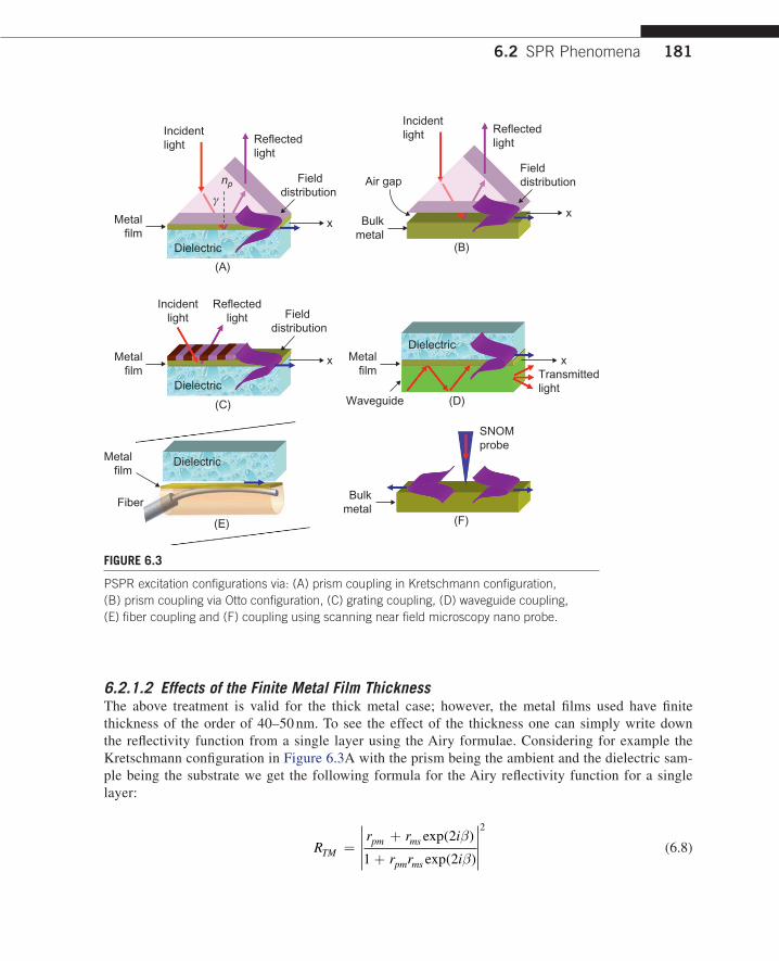
181
6.2.1.2 Effects of the finite Metal film thicknessThe above treatment is valid for the thick metal case; however, the metal films used have finite thickness of the order of 40–50 nm. To see the effect of the thickness one can simply write down the reflectivity function from a single layer using the Airy formulae. Considering for example the Kretschmann configuration in Figure 6.3A with the prism being the ambient and the dielectric sam-ple being the substrate we get the following formula for the Airy reflectivity function for a single layer:
Rr r i
r r iTMpm ms
pm ms
=+
+
exp( )
exp( )
2
1 2
2
(6.8)
Fielddistribution
Dielectric
Metalfilm
Incidentlight
γ
Reflectedlight
x
(A)
Fielddistribution
Bulkmetal
Incidentlight Reflected
light
x
(B)
Air gap
Field distribution
Dielectric
Metalfilm
Incidentlight
Reflectedlight
x
(C) Waveguide
Metalfilm Transmitted
light
x
(D)
Dielectric
Dielectric
Fiber
Metalfilm
(E)
Bulkmetal
(F)
SNOMprobe
np
FIgURE 6.3
PSPR excitation configurations via: (A) prism coupling in Kretschmann configuration, (B) prism coupling via Otto configuration, (C) grating coupling, (D) waveguide coupling, (E) fiber coupling and (F) coupling using scanning near field microscopy nano probe.
6.2 SPR Phenomena

182 CHAPTER 6 Plasmonics
where = k dzm m is the single-pass phase factor through the metal film and rlj are the Fresnel reflection coefficients from medium j m s= , when the light is incident from medium l p m= , , with the subscript p standing for prism. For TM waves the Fresnel coefficients may be expressed as:
rk k
k kljzl l zj j
zl l zj j
=/ /
/ /
ε ε
ε ε
−
+
(6.9)
where k k kzj j x= −ε 02 2 . Figure 6.4 shows reflectivity curves versus the incidence angle in the
prism at different metal film thicknesses showing that there is an optimum thickness at which RTM min = 0.
The dispersion relation of the single-layer system is determined by the poles of the reflectivity function, hence it is given by:
1 2 0+ =r r ipm ms exp or( )
(6.10)
( )( )
( )(
k k k k
k k k kzp p zm m zm m zs s
zp p zm m zm m zs
/ / / /
/ / / /
ε ε ε εε ε ε+ + +− − εε s i)exp( )2 0=
(6.11)
0
0.2
0.4
0.6
0.8
1
45 60 75 90
Incidence angle (deg)
TM
ref
lect
ivity
38nm
48 nm
58 nm
FIgURE 6.4
TM reflectivity versus incidence angle for Kretchmann configuration at different metal film thicknesses using wavelength 653 nm, prism index of 1.515 (BK7), water analyte (substrate) with index of 1.33. The metal index used is: 0.14 + 4.2i.
183
This equation can be split into two dispersion relations describing two surface plasmons excited at both sides of the metal film. Since kzm is mainly imaginary then is mainly imaginary and for thick enough metal Eq. 6.11 yields the following two equations:
k kzp p zm m/ /ε ε+ = 0
(6.12)
k kzm m zs s/ /ε ε+ = 0 (6.13)
These two dispersion relations are similar to relation (2) and therefore represent two SP waves excited at the two metal film interfaces having radial frequencies of:
εSP
p
p1
1=
+
(6.14)
εSP
p
s2
1=
+
(6.15)
For the case of thin metal film surrounded by the same medium of dielectric constant εs the two equations are:
ε ε ε
+ +
− −
= + =
=
: Im( ) Im( ) tanh(Im( ) )
: Im(
L k k k d
L kmr zs s zm zm m
mr
/2 0
zzs s zm zm mk k d) Im( )coth(Im( ) )+ =ε /2 0
(6.16)
The symmetry in both sides of the film causes the two plasmons to have the same SPR frequency. The upper branch is an asymmetric mode (with respect to z = 0) while the lower branch is symmetric. The asymmetric mode then has zero energy at the center of the metal film while the symmetric mode has its maximum at the center of the metal film at z dm= /2. As a result the latter gets absorbed quickly while the former propagates for longer distance along the interface forming what is called long-range surface plasmon (LRSP).
In order to excite the additional SPR a dielectric layer has to be inserted between the prism and the metal film having an index less than that of the prism as shown in the inset in Figure 6.5. Figure 6.5B shows the single SPR and double SPR excitations for this geometry with and without the buried dielectric layer respectively. Note that the single SPR dip location is not sensitive to the insertion of the buried dielectric layer. This is because for this plasmon the energy is concen-trated mainly on the metal–analyte interface. In order to show further at which interface each of the SPRs are excited, the effect of the variation of the refractive index of the analyte na and the buried dielectric layer index nb on the double SPR spectrum was calculated and is shown in Figure 6.7. In each case only one SPR dip is affected but not the other, thus proving that the first dip is excited
6.2 SPR Phenomena
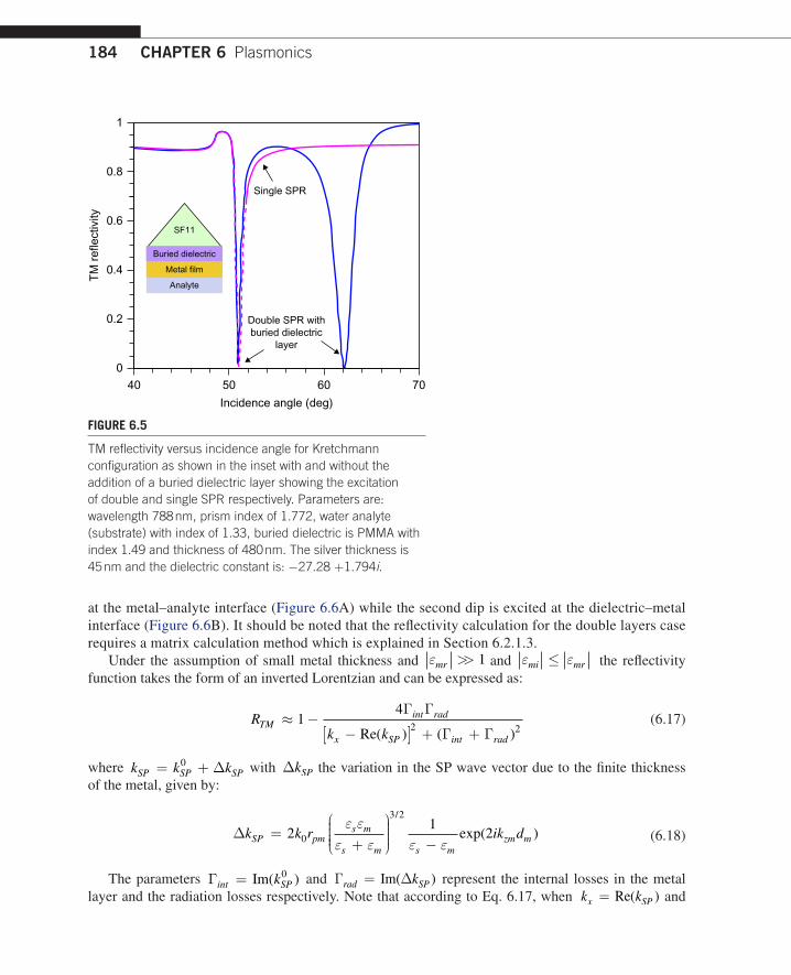
184 CHAPTER 6 Plasmonics
at the metal–analyte interface (Figure 6.6A) while the second dip is excited at the dielectric–metal interface (Figure 6.6B). It should be noted that the reflectivity calculation for the double layers case requires a matrix calculation method which is explained in Section 6.2.1.3.
Under the assumption of small metal thickness and εmr >> 1 and ε εmi mr≤ the reflectivity function takes the form of an inverted Lorentzian and can be expressed as:
Rk k
TMint rad
x SP int rad
≈ −−[ ] + +
14
2 2
Γ Γ
Γ ΓRe( ) ( )
(6.17)
where k k kSP SP SP= +0 ∆ with ∆kSP the variation in the SP wave vector due to the finite thickness of the metal, given by:
∆k k r ik dSP pms m
s m s mzm m=
+
−
21
20
3 2ε εε ε ε ε
/
exp( )
(6.18)
The parameters Γint SPk= Im( )0 and Γ ∆rad SPk= Im( ) represent the internal losses in the metal layer and the radiation losses respectively. Note that according to Eq. 6.17, when k kx SP= Re( ) and
0
0.2
0.4
0.6
0.8
1
40 50 60 70
Incidence angle (deg)
TM
ref
lect
ivity
Double SPR withburied dielectric
layer
Single SPR
SF11
Buried dielectric
Metal film
Analyte
FIgURE 6.5
TM reflectivity versus incidence angle for Kretchmann configuration as shown in the inset with and without the addition of a buried dielectric layer showing the excitation of double and single SPR respectively. Parameters are: wavelength 788 nm, prism index of 1.772, water analyte (substrate) with index of 1.33, buried dielectric is PMMA with index 1.49 and thickness of 480 nm. The silver thickness is 45 nm and the dielectric constant is: −27.28 +1.794i.

185
Γ Γint rad= the reflectivity becomes zero and the plasmon is excited. When only the wave vector matching is satisfied, k kx SP= Re( ), the minimum reflectivity level at the dip becomes:
RTMint rad
int radmin
( )≈ −
+1
42
Γ Γ
Γ Γ
(6.19)
In Figure 6.4 the effect of the wave vector mismatch on the reflectivity due to slight variation of the metal film thickness is shown. Note that according to Eq. 6.18, the effect of the metal thickness is to
0
0.2
0.4
0.6
0.8
1
40 50 60 70
Incidence angle (deg)
TM
ref
lect
ivity
nb = 1.49
na = 1.37 nb = 1.49
na = 1.33
(A)
0
0.2
0.4
0.6
0.8
1
40 50 60 70
Incidence angle (deg)
TM
ref
lect
ivity na = 1.33
nb = 1.49
na =1.33 nb =1.53
(B)
FIgURE 6.6
Effect of variation of the index of the analyte na (A) and the buried dielectric layer nb on the double SPR spectrum. In each case only one SPR dip is affected but not the other, thus proving that the first dip is excited at the metal–analyte interface while the second dip is excited on the dielectric–metal interface. Other parameters are the same as in Figure 6.5.
6.2 SPR Phenomena

186 CHAPTER 6 Plasmonics
add phase accumulation via the optical path length of the metal film. Hence the effect on kSP is an interference effect which is minimized when Re ∆kSP{ } = 0, that is the total phase of ∆kSP is ( )2 1 2m − π/ with m being an integer. This indicates that the optimum SPR is obtained when a cavity-like mode is excited in the thin metal film, a fact that can be understood also from the existence of a pole in the reflectivity function, which is a neces-sary condition for the excitation of a surface wave.
At the optimum, Eq. 6.3 is satisfied, which in the Kretschmann configuration one can write k k nx p= 0 sinγ giving the following expression for the resonance angle:
γε εε ε
=+
arcsin1
1 2
np
mr s
mr s
/
(6.20)
For grating coupling (Figure 6.3C) with the light incident at an angle γ from an incidence medium with index ni we have: k k n mGx i= +0 sin γ where G = 2π/ is the grating vector. The wave vector matching condition then becomes:
n mimr s
mr s
sin γλ ε ε
ε ε+ =
+
1 2/
(6.21)
where m here is the diffraction order.For the calculation of the reflectivity from the double layer problem we used the Abeles charac-
teristic matrix approach. This approach is very useful for multilayered structures and therefore we describe it in detail below.
6.2.1.3 the 2 × 2 Abeles Matrix Approach for the optics of MultilayersConsider the general case of a plane EM wave interacting with a stack of N − 1 layers as shown in Figure 6.7 so that there are N interfaces. The layers are homogeneous and isotropic with plane bounda-ries, and the optical properties of each layer j are characterized completely by two constants which are functions of wavelength, e.g. the dielectric constant ε j and the magnetic permeability µ j so that the refractive index is nj j j= ε µ .
The plane of incidence is taken to be the xz-plane and the z axis is the direction of stratification. For TM wave, H Hx z= = 0 and Ey = 0 . The non-vanishing components of the field vectors into each layer j are of the form:
HE
yj yj j
xj xj
x z t H z i k x t
x z t E z i k
( , , ) ( )exp ( )
( , , ) ( )exp (
= −{ }=
0
0
α
α jj
zj zj j
x t
x z t E z i k x t
−{ }= −{ }
α
)
( , , ) ( )exp ( )E 0
(6.22)
n1, d1
n2, d2
X
Y
Z
nN−1, dN−1
n0Z1 = 0
Z2
Z3
ZN−1
ZN
nN
θ0
θN
FIgURE 6.7
Schematic of a multilayer system composed of (N – 1) homogeneous and isotropic media with N interfaces bounded by two semi-infinite homogeneous, isotropic media.

187
Here H z E z E zyj xj zj( ), ( ), ( ) are the amplitudes of the appropriate fields into layer j that are in general complex functions of z; α θj j jn= sin with θ j being the propagation angle. According to Snell’s law one can write:
α θ α θj j jn const n= = = =sin sin0 0 (6.23)
From Maxwell’s equations H z E zyj xj( ), ( ) satisfy the following first-order system of differential equations [3]:
d
dz
H
E
ik z
ik zz
yj
xj jj−
=
⋅ −
0 0
0
2
ε
µα
ε
( )
( )( )
⋅−
0
H
E
yj
xj
(6.24)
Eqs. 6.24 are obtained from decomposition of Maxwell’s equations into six scalar equations for the field components. The amplitudes of the electric field E z E zxj zj( ), ( ) are related by means of the equation:
α εj xj j zjE z E⋅ + ⋅ =( ) 0
(6.25)
Direct integration of the differential equations system (Eq. 6.24) for the homogeneous case yields the well-known Abeles matrix form solution connecting the tangential field amplitudes at the entrance of each layer to the field amplitudes at a distance z inside the layer:
H
EM
H z
E z
i
qyj
xj
jyj
xj
jj
0
0−
= ⋅
−
=
−( )
( )
cos si nn
sin cos
( )
( )
j
j j j
yj
xjiq
H z
E z−
⋅−
(6.26)
H Eyj xj0 0, are the amplitudes of H Eyj xj, respectively at the appropriate boundary z Z j= of layer j,
M j is called the characteristic matrix for the layer j and it is determined by the optical properties and the layer thickness where:
θµ
εθj j j j j
j
jjk n d q= =0 cos , cos
(6.27)
For a multilayered structure the field amplitudes at the first boundary are connected to those at the last one by the total characteristic matrix:
H
EM
H
EM M
y
x
TOTyN
xN
TOT jj
j N1
0
10
0
01−
= ⋅
−
==
=
,−−
∏1
(6.28)
6.2 SPR Phenomena

188 CHAPTER 6 Plasmonics
The complex reflection and transmission coefficients r and t respectively can be expressed in terms of the elements of the total characteristic matrix of the whole system Mij:
rM M q q M M q
M M q q M M qN N
N N
=+ ⋅ ⋅ − + ⋅+ ⋅ ⋅ + + ⋅
( ) ( )
( ) ( )11 12 0 21 22
11 12 0 21 22
ttq
M M q q M M qN N
=⋅
+ ⋅ ⋅ + + ⋅2 0
11 12 0 21 22( ) ( )
(6.29)
For TE polarization all the expressions for the characteristic matrix and reflection or transmission
coefficients are valid simply by replacing the expression for qjj
jj= ⋅
µ
εθcos with pj
j
jj= ⋅
ε
µθcos
and the field column for TE is E
H
yj
xj
. The energy reflection coefficient is R r= 2 while the energy
transmission coefficient is:
T tN
N
=
Re
cos
cos
η θη θ
0
0
2
(6.30)
where ηµ
εjj
j
= is the impedance of medium j. In a similar manner for the single-layer case, for
multilayered structure, the poles of the reflectivity function determine the SPR locations and by equat-ing the denominator of r to zero one can derive the dispersion relation.
6.2.1.4 the field Distribution CalculationThe EM field distribution inside the metal or the dielectric is of high importance as it teaches us where most of the energy is concentrated. If the energy is mostly in the metal the plasmon will be absorbed within a short distance, while if the energy is mostly in the dielectric, it will propagate for a longer distance along x and its interaction with the dielectric will be maximized. Using the same nomenclature as in the previous subsection the following three-step algorithm was developed by Shalabney and Abdulhalim [4]:
Step 1: Calculating the reflection coefficient from the whole structure according to Eq. 6.29.Step 2: Calculating the field within the first layer:
H z
E zP z
r H
r E
y
x
yinc
xinc
1
11
1
1
( )
( )( )
−
= ⋅
+( )
−( )
≤ ≤, Z z Z1 2
(6.31)
where P z1( ) is given by:
P zk n z
i
qk n z
iq k n z1
0 1 11
0 1 1
1 0 1 1
( )cos cos sin cos
sin cos c
=( ) ( )
( )
θ θ
θ oos cosk n z0 1 1θ( )
(6.32)
and the incident fields are related by the relation: E q Hxinc
yinc= 0 .
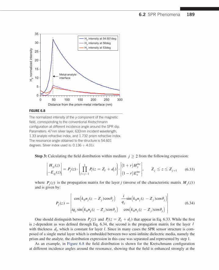
189
Step 3: Calculating the field distribution within medium j ≥ 2 from the following expression:
H z
E zP z P z Z d
yj
xjj l l l
l j
( )
( )( ) ( )
−
= ⋅ = +
= −∏
1
1⋅+( )
−( )
≤ ≤ +
1
11
r H
r EZ z Z
yinc
xinc j j,
(6.33)
where P zj ( ) is the propagation matrix for the layer j (inverse of the characteristic matrix M zj ( ) ) and is given by:
P zk n z Z
i
qk n z Z
iq k nj
j j jj
j j j
j
( )cos ( )cos sin ( )cos
sin
=−( ) −( )0 0
0
θ θ
jj j j j j jz Z k n z Z( )cos cos ( )cos−( ) −( )
θ θ0
(6.34)
One should distinguish between P zj ( ) and P z Z dl l l( )= + that appear in Eq. 6.33. While the first is z-dependent as was defined through Eq. 6.34, the second is the propagation matrix for the layer l with thickness dl, which is constant for layer l. Since in many cases the SPR sensor structure is com-posed of a single metal layer which is embedded between two semi-infinite dielectric media, namely the prism and the analyte, the distribution expression in this case was separated and represented by step 1.
As an example, in Figure 6.8 the field distribution is shown for the Kretschmann configuration at different incidence angles around the resonance, showing that the field is enhanced strongly at the
0
5
10
15
20
25
30
35
0 50 100 150 200 250 300
Distance from the prism-metal interface (nm)
Hy
norm
aliz
ed in
tens
ity
Hy intensity at 54.601deg
Hy intensity at 56deg
Hy intensity at 53deg
Metal-analyteinterface
FIgURE 6.8
The normalized intensity of the y component of the magnetic field, corresponding to the conventional Kretschmann configuration at different incidence angle around the SPR dip. Parameters: 47 nm silver layer, 633 nm incident wavelength, 1.33 analyte refractive index, and 1.732 prism refractive index. The resonance angle obtained to the structure is 54.601 degrees. Silver index used is: 0.136 + 4.01i.
6.2 SPR Phenomena

190 CHAPTER 6 Plasmonics
resonance. This field enhancement is a result of the confinement of the field to a small region near the surface when the plasmon is excited. Another example is shown in Figure 6.9 for the case of double SPR excitation as in Figure 6.5, show-ing that for the first resonance (smaller resonance angle) the field is enhanced at the metal–analyte interface while for the second resonance it is enhanced at the buried dielectric–metal interface.
6.2.2 Localized SPRWhen the metal is composed of subwavelength structural units such as nanoparticles or containing nanoholes, array of lines, etc., the SP wave can-not propagate more than the size of this structural unit, hence it becomes localized. One of the most attractive aspects of these collective excitations is their use to concentrate light in subwavelength structures and to enhance transmission through periodic arrays of subwavelength holes in opti-cally thick metallic films. SPs are tightly bound to metal–dielectric interfaces penetrating around
10 nm into the metal (the so-called skin depth) and typically more than 100 nm into the dielectric (depending on the wavelength). SPs at the optical wavelengths concentrate light in a region that is considerably smaller than their wavelength, a feature that suggests the possibility of using surface–plasmon polaritons for the fabrication of nanoscale photonic circuits operating at optical frequencies. In addition the possibility of manufacturing such nanobeds in planar form makes them remarkably important for biosensing towards biochip application.
6.2.2.1 Absorption and Scattering by Metal NanospheresThe simplest case is a metallic sphere of radius R embedded in a medium with dielectric constant εd. Since the magnitude of the electric field seems static around the nanoparticle in the limit of R<<λ, Maxwell’s equations can be solved in the quasi-static approximation. The solution of the Laplace equation for the static potential inside the sphere is [5,6]:
φ θ ϕ θ ϕ( , , ) ( , ),r a r Y r Rlml
lmm l
l
l
= ≤ ≤=−=
∞
∑∑0
0
(6.35)
where r, ,θ ϕ are the radial, polar and azimuthal coordinates accordingly; Y lm ( , )θ ϕ is the spherical harmonic function. Outside the sphere the solution is:
φ θ ϕ θ ϕ( , , ) ( , ),r br
Y r Rlm l lmm l
l
l
= ≥+
=−=
∞
∑∑ 11
0
(6.36)
0
10
20
30
40
50
0 150 300 450 600 750 900
Distance from the prism interface (nm)
Hy
norm
aliz
ed in
tens
ity
Hy−50.945degHy−62.14deg
Dielectricmetal interface
Metalanalyteinterface
FIgURE 6.9
The normalized intensity of the y component of the magnetic field, corresponding to the Kretschmann configuration with double SPR excitation by adding buried dielectric layer as in Figure 6.5. The resonance angles for each SP wave are indicated in the figure. Parameters are the same as in Figure 6.5.

191
The solutions in Eqs. 6.35 and 6.36 vanish at the center of the sphere and at infinity accordingly. The continuity condition on the surface for the potential and its derivative ε∂ ∂ϕ/ r leads to the following dispersion relation:
εε
m
d
l
l++=
10
(6.37)
Using the Drude form for metal dispersion we get:
εl p
d
l
l l=
+ +
( )1
1 2/
(6.38)
where l is a positive integer. The case with the lowest-order mode l = 1 describes the dipole active mode which is the most significant for small spheres. On the other hand, for the case of a large sphere, higher-order modes are significant, that is l → ∞, the resonance frequency becomes ε∞ = +p d/ 1 , which is just the SP frequency for the case of semi-infinite metal–dielectric interface.
For the lowest-order case, the form of the EM field outside the sphere will be:
E x y z E z a Ez
r
z
rxx yyout
m d
m d
( , , ) = −−+
⋅ ⋅ − +0
30 3 52
3ˆˆ
ˆ ˆε εε ε
++( )
zz
(6.39)
where E0 is the applied field magnitude which is polarized in the z direction in this case. The EM field displaces the free electron cloud and produces uncompensated charges near the particle surface and corresponding opposing forces (as in Figure 6.10). The optical resonance related to these oscil-lations is called the localized SPR (LSPR). The origin of the term “surface” is from the knowledge that the oscillations are caused by the polarization of the particle surface, and because the generated
−−−
−−−
+++
−−−
+++
+++
−−−
+++
Electron cloud
Metal sphere
Applied electric field
Time
FIgURE 6.10
Oscillations of free electrons at the surface of a nanosphere due to applied electric field with arbitrary polarization.
6.2 SPR Phenomena

192 CHAPTER 6 Plasmonics
electric field is larger near the particle surface and decays far from the surface, which makes it similar to the evanescent field at flat interface in the propagating SPR case. In the general case, the frequency of the collective oscillations does not coincide with the applied wave frequency and is determined by many factors, the electron concentration, electron effective mass, the particle shape and size, interac-tion between particles, and the influence of the environment. However, for the elementary description of the nanoparticles plasmon resonance it is sufficient to use the usual dipole approximation, and the Drude model.
Within the dipole approximation the absorption and scattering of light by a small particle are determined by the electrostatic polarizability of the particle α0 , which can be calculated using the metal optical permittivity ε m ( ), the medium dielectric constant εd , and the particle geometrical dimensions [7]:
απε εε ε
ε εε ε0
33
4 2 2=
−+
=
−+
Vam d
m d
m d
m d
(6.40)
Using the renormalized polarizability to be consistent with the energy conservation law, the inte-grated absorption and scattering cross-sections are calculated based on Mie scattering theory to be:
C C Ck
ak kext abs sca
d m
m d
= + =( )−
⋅ + ≅12 8
34
3 2
2 4 2π ε ε
ε εα
πα π α
ImIm( )
(6.41)
here k d=2π ε
λ is the wave number in the medium, and the static and renormalized polarizabilities
(α0 and α) are related by:
αα
φ α=+ ⋅ ⋅−
03
01 ( )ka a
(6.42)
where the function φ ka ka i ka( ) ≅ −( ) − ( )2 32
3 takes into account the radiative decay.
The constants C C Cabs sca ext, , are the absorption, scattering and total cross-sections respectively. The results above are calculated with Mie scattering formalism for spherical particles. Below we will distinguish between the static polarizability and the renormalized polarizability. In the static case the extinction cross-section will be [8]: C kext ≅ =( )4 0π α αIm . One can see from the latter expression that the extinction spectrum has a strong resonance when:
ε εm res d=( ) = −2
(6.43)
Although the well-known Drude model describes the permittivity of bulky metal, we will use it for estimating the resonance frequency:
ε ε
γm ibp
bi( ) = −
+( )
2
(6.44)
193
where εib is the contribution of the interband electronic transitions and γb is the volume decay con-stant. Unlike the case of extended SPR, here we consider the exact Drude model because the metal permittivity has a main role in determining the LSPR frequency. Substituting Eq. 6.44 into Eq. 6.43 with the assumption that the significant contribution to the extinction spectrum is caused by absorp-tion, we can express the effective absorption cross-section by the resonance frequency and the metal characteristics:
C aka
absd
d ib
p b b
b res
=+
⋅+
+ − +π
ε
ε ε
γ γ
γ 2
2
2 2
2 2 2 2
12
2( )
( )( )
( )
/
rres b4 2 2⋅ γ /
(6.45)
where the resonance frequency res and the corresponding resonance wavelength λres are given by:
ε ελ λ ε εres
p
ib dres p ib d=
+= ⋅ +
22; (6.46)
Here λp is the plasma wavelength, λπp
p
c=
2. It was demonstrated [9,10] that near the resonance, the
absorption spectrum can be approximately reduced to a Lorenzian profile for the purpose of compari-son between small metallic nanoparticle permittivity and the same metallic bulk permittivity.
Since the Drude model mainly uses the Maxwell equations and the boundary conditions, it is con-sidered as a classical approach to describe the permittivity function of the metal and the dependence on the angular frequency. This model is usually used for bulk samples and it becomes problematic for very small particles. In this context, many studies were done on adjusting the classical model also to small nanoparticles. The modification was done by means of correction function added to the permit-tivity function which considers the dependence on the particle size [11–14]. A comprehensive study was done recently in several review articles [7,15,16].
6.2.2.2 Absorption and Scattering by Anisotropic NanoparticlesSo far we have considered the case of a small metallic sphere. In the general case the LSPR can be excited in many other structures and shapes [17]. In most cases metal particles are not isolated and not purely spherical. The fact that metallic particles aggregate and form a large and more compli-cated structure does not change their strong absorption and scattering properties that we mentioned above; the difference may be the number of the absorption peaks within the frequency range. One of the most general descriptions of a smooth and regular shape is an ellipsoid with three axes a b, and c a b c ( )≥ ≥ . If b c= , the ellipsoid becomes a prolate spheroid (cigar shape), and if a b= the ellipsoid becomes oblate spheroid (pancake shape). In a similar manner we can define polarizability for the structure in each direction of the major axes of the ellipsoid. Namely the polarizability that an applied electric field produces depends on the polarization direction of the external applied field, and consequently the resonance wavelength is determined for each axis i, when the electric field is polar-ized along that particular axis:
απ ε ε
ε ε εim d
i m d d
abc
L=
−−( ) +
4
3
(6.47)
6.2 SPR Phenomena

194 CHAPTER 6 Plasmonics
where Li is a form factor of axis i when the electric field is polarized along this axis and αi is the polarizability corresponding to the same axis. The geometrical factors Li obey the follow-ing rules 0 1≤ ≤Li and L L La b c+ + = 1 when considering the axes a, b, and c. For a sphere
L L La b c= = =1
3 due to spherical symmetry and then Eq. 6.40 is satisfied. The absorption cross-
section when the applied field is polarized parallel to the i axis will then be:
C kabs i= ( )Im α
(6.48)
Now, there are peaks in the absorption spectra when ε εd miL
= −
11
[18]. Since 0 1≤ ≤Li ,
the term 1
Li
yields a wide range of frequencies (see Figs. 6.11–6.13). Similar behavior for nanodiscs
and nanorods can be obtained because they are the limits of oblate and prolate spheroids respectively. Furthermore, one can describe the response of structures in terms of ellipsoids with various shapes. In Figures 6.11, 6.12 and 6.13 several examples of the absorption cross-section are shown for spheres, prolate and oblate spheroids respectively.
One can design the resonance frequency by tailoring the shape and the size of the nanoparticles. In Figures 6.12 and 6.13, the absorption cross-section was calculated for silver nanospheroids with vari-ous shapes and sizes. The peak can be red-shifted or blue-shifted compared with the peak of a sphere by controlling the size and the shape of the spheroid. The geometrical factors Li can be analytically calculated for standard smooth particles like spheres, spheroids, ellipsoids, and cylinders. In the work that was done by Stoner [19], the geometrical factors for ellipsoids were calculated, and the elliptic
0
0.2
0.4
0.6
0.8
100 200 300 400 500 600 700Wavelength (nm)
Abs
orpt
ion
cros
s se
ctio
n (µ
m2 )
Silver
Gold
FIgURE 6.11
Absorption cross-section for silver and gold spheres. Both silver and gold spheres are with 100-nm diameter and embedded in air; the y axis is normalized to 10–12 m2.

195
0
10
20
30
40
50
60
70
0
0.5
1
1.5
2
2.5
3
100 300 500 700 900Wavelength (nm)
L = 500 nm S = 100 nm
L = 550 nm S = 75 nm
L = 500 nm S = 75 nm
L = 500 nm S = 100 nm
L = 550 nm S = 75 nm
L = 500 nm S = 75 nm
ExcitationExcitation
Cab
s fo
r sh
ort a
xis
(µm
2 )
Cab
s fo
r lo
ng a
xis
(µm
2 )
FIgURE 6.12
Absorption cross-section calculated using 7.47 and 7.48 for prolate silver spheroids in air with different axis lengths. L indicates the long axis of the spheroid and S indicates the short axis of the spheroid. For each combination of long and short axes, the absorption was calculated for both the polarization parallel to the long axis (solid curves) and parallel to the short axis (dashed curves).
0
20
40
60
80
100
120
140
160
180
0
2
4
6
8
10
12
100 300 500 700 900
Wavelength (nm)
Cab
s fo
r lo
ng a
xis
(µm
2 )
Cab
s fo
r sh
ort a
xis
(µm
2 )
ExcitationExcitation
L = 500 nm S = 100 nm
L = 550 nm S = 75 nm
L = 500 nm S = 75 nm
L = 500 nm S = 100 nm
L = 550 nm S = 75 nm
L = 500 nm S = 75 nm
FIgURE 6.13
Absorption cross-section calculated using 6.47 and 6.48 for oblate silver spheroids in air. For each spheroid, the absorption was calculated for both the polarization parallel to the long axis (solid curves) and parallel to the short axis (dashed curves). The right vertical scale corresponds to the long axis polarization, and the left vertical scale corresponds to the short axis polarization. Same other parameters as in Figure 6.12.
6.2 SPR Phenomena

196 CHAPTER 6 Plasmonics
integrals can be explicitly solved for spheroids. In the case of prolate spheroid with a being the major
long axis and b c= the equatorial short axes, we define eb
a≡ −
1
2
, and then the appropriate
geometrical factors will be:
L
e
e e
e
eL L La b c a=
− +−
−
= = −
1 1
2
1
11
1
21
2
2ln ( )and
(6.49)
where La is the geometrical factor when the excitation polarization is along the major long axis, and L Lb c= are the geometrical factors when the excitation is along the equatorial short axes b or c . In the case of oblate spheroid, when a b= are the equatorial long axes, and c is the short polar axis, if we
define ec
a≡ −
1
2
, the appropriate factors will be:
Le
e
ee L L Lc a b c= −
−
= = −1
11 1
21
2
2 1 2( )arcsin( ) ( )
/
and (6.50)
For other complicated geometries, researchers have developed numerical methods to calculate the form factors such as the discrete dipole approximation method and the finite-difference time-domain (FDTD) method. In these methods, the particle is represented as a large finite number of elements, each of which can interact with the applied electric field. In the case of discrete dipole approximation, this interaction is modeled in the frequency domain, whereas the finite-difference time-domain evalu-ates this interaction in the time domain. In addition to modeling the extinction spectrum of nanoparti-cles, several equations describe how the LSPR is used for sensing. For example, the LSPR extinction resonance frequency is sensitive to the medium dielectric constant εd (or refractive index, nd ) according to Eqs. 6.46–6.48. Thus, changes in the environment (by adding adsorbate layer for exam-ple) cause an appropriate shift in the resonance wavelength. The relationship between perturbations in the dielectric medium refractive index ∆nd and the sensitivity of the shift in the resonance wave-length ∆λres with respect to a change in the refractive index ∆nd of the adsorbate is given by:
Sn
Sd
lres
dbulk
dλ λ
λ= = −
−
−∆∆
12
exp
(6.51)
where S bulkλ− is the bulk refractive index response of the nanoparticles (sensitivity) and ld is the characteristic EM field decay. The latter equation matches most of the experiment results, and forms the bases of LSPR sensing mechanism.
6.2.2.3 field Enhancement and Surface-Enhanced optical EffectsAccording to Eq. 6.47, there are peaks in the absorption cross-section when:
ε εd mriL
= −
11
(6.52)

197
These peaks originate from the form of the polarizability, which is proportional to the local elec-tromagnetic field. Hence at the LSPR resonance there is a local field enhancement. Rigorous cal-culations indeed show field enhancement by three orders of magnitude in the nm vicinity of the nanoparticle and then decay exponentially within ld ≈ 10 100– nm. One can visualize this pheno-menon by considering the nanoparticle as localizing the electric field of a dipole field centered in the sphere, which then decays with the dipole decay law away from the surface in all directions. In this sense, the nanoparticle acts as an antenna which amplifies the intensity of the scattered light.
These local field enhancements cause enhancements in different optical phenomena such as sec-ond harmonic generation (SHG), surface-enhanced fluorescence (SEF) and surface-enhanced Raman scattering (SERS). Since in these optical phenomena the output intensity depends on the excitation field to some power, their signal is enhanced considerably. For example, for SERS the intensity is pro-portional to the fourth power of the field E
4; one then can obtain enhancement of the order of 1012.
Fluorescence intensity is on the other hand proportional to E2, so that the maximum enhancement
factor can be 106, although experiments reported much less than this factor (up to 1000 at most) because fluorescent dyes are chemically affected by their metallic neighborhood in addition to bleach-ing which takes place within a short time when the excitation field is enhanced.
6.2.2.3.1 SERSThe signal enhancement is so dramatic that very weak Raman peaks that are unnoticeable in sponta-neous Raman spectra can appear prominently enough in SERS spectra. Some trace contaminants can also contribute additional peaks. Moreover, because of chemical interactions with metal surfaces, cer-tain peaks that are strong in conventional Raman spectra might not be present in SERS spectra at all. The non-linear character of signal intensity as a function of the concentration complicates things even further. Very careful consideration of all physical and chemical factors must be made while interpret-ing SERS spectra, which makes it extremely impractical.
Although a complete understanding of SERS has not been achieved yet, two main mechanisms are widely accepted. The first, called chemical enhancement, involves enhancement of polarizability of the analyte molecule that may occur because of a charge-transfer effect or chemical bond forma-tion between the metal surface and the analyte molecules. The second is due to the enhanced electro-magnetic field produced at the surface of the metal when the wavelength of the incident light matches the SPR wavelength of the metal. Molecules adsorbed or in close proximity to the metal surface expe-rience an exceptionally large electric field. Because the Raman effect is proportional to the fourth power of the field amplitude, the efficiency is enhanced by factors as large as 1014. Molecular vibra-tional modes normal to the metal surface are most strongly enhanced in comparison to other vibra-tional modes. Electromagnetic simulations confirm that the electric field can be enhanced [20,21] by a factor of 103 and so the Raman signal is enhanced by a factor of 1012.
The SPR intensity is dependent on many factors, including the wavelength of the incident light and the morphology of the metal surface. The Raman excitation wavelength should match the plasma wavelength of the metal, which is about 382 nm for a 5-m silver particle but can be as high as 600 nm for larger ellipsoidal silver particles. The plasma wavelength shifts to 650 nm for copper and gold, the other two metals that are used for SERS at wavelengths in the range from 350–1000 nm. The best modality for SPR excitation is the use of either a nanoparticle (<100 nm diameter) or an atomically rough surface.
6.2 SPR Phenomena
198 CHAPTER 6 Plasmonics
The Raman scattering from a compound (or ion) adsorbed on or even within a few angstroms of a structured metal surface can be enhanced by factor of 103 to 1014 compared to the case when it is in a solution. SERS is strongest on a silver surface [22,23], but is observable on gold and copper surfaces as well, and it is now known that the shape of the nanoparticle plays a crucial role in determining the enhancement factor. The triangular-pyramid shape has been found to give the strongest enhancement. SERS was discovered with pyridine. Other aromatic nitrogen- or oxygen-containing compounds, such as aromatic amines or phenols, also display strong enhancement due to SERS. The enhancement can also be seen with other electron-rich analytes such as carboxylic acids. Although SERS allows easy observation of Raman spectra from solutions with concentrations in the micromolar (10–6) range, slow adsorption kinetics and competitive adsorption limit its application in analytical chemistry.
6.2.2.3.2 SEFSurface-enhanced fluorescence (SEF) has been known for more than a few decades now [24], but its potential was rediscovered during the last decade due to the emerging developments in the field of optics of metallic nanostructures [25,26]. SEF is fundamentally interesting because several effects play a role in it, and it can be achieved even with exciting photon energies far from the surface plas-mon resonance (SPR). SEF is a very useful phenomenon, with significant applications in biotechnol-ogy and life sciences, alongside surface-enhanced Raman scattering (SERS).
When a molecule is excited, there are a variety of processes which will return it to the ground state. If we consider three processes for returning to the ground state (radiationless energy loss, inter-system crossing through the triplet state, and emission of photons) then the efficiency of emission will be a function of the competing rates of these processes:
η =
+ +
K
K K Kf
f i x (6.53)
where η is efficiency or quantum yield which is a dimensionless quantity given by the ratio between the emitted photon and the number of absorbed photons. The rate constants K f i x, , designate those for fluorescence emission, without any radiation energy loss, and intersystem crossing, respectively. The average lifetime of the excited state is inversely related to the fluorescence emission rate: τ f fK= −1.
Surface-enhanced fluorescence (SEF) takes place in the proximity of metal structures. In the prox-imity of metals, the fluorophore radiative properties are modified and an increase in the spontaneous emission rate is observed, which is associated with a concomitant increase in the radiative quantum efficiency. This results from the shortening of the fluorescence lifetime, which enables faster cycling of the fluorophore. These are given by the following relationships:
ηns
f ns
f ns i x
K K
K K K K=
+
+ + +
(6.54)
τns
f nsK K=
+1
(6.55)

199
Here, ηns is the quantum yield, modified by the nanostructure, k f and ki are rate constants, Kns is the additional rate constant induced by the nanostructure and τns is the fluorophore lifetime modified by the nanostructures.
SEF is a very useful phenomenon with significant applications in biotechnology [25] and life sci-ences, alongside surface-enhanced Raman scattering (SERS). Several physicochemical effects [27–34] related to the behavior of fluorophores near nanoparticles have been brought into focus by the emerg-ing field of plasmonics. The effect of surfaces near an oscillating dipole on its emission properties was first investigated by Chance et al. [24], which led to the development of the Chance–Prock–Silbey (CPS) theory. The most important consequences of the CPS theory are as follows: (1) The reflected field from the nearby interface interferes with the emitted field and, therefore, can enhance or weaken the fluorescence depending on the distance between the dipole and the interface. (2) When the nearby surface is more reflective, the enhancement factor is larger. (3) Very close to a reflective surface, the excited molecule may decay non-radiatively by coupling to lossy modes, SPs or guided waves. This coupling may even quench the fluorescence when the molecule is touching the interface. (4) At small distances near a metallic surface, the lifetime decreases due to several competing relaxation proc-esses. (5) In SP cross emission (SPCE), one way to excite SEF, the excited SPs couple back to the radiative electromagnetic mode on the back side of a metal film [35] (Kretschmann configuration or rough metal surfaces). On top of these effects, localization of the electromagnetic field near nano tips, corners, holes, needles, etc. has been shown to produce large SEF by factors up to a few hundred in what is known as the lightning nano-antenna effect [36].
The quantum efficiency of the photoluminescence (PL) from a bulk noble metal is very low (typi-cally 10−10). However, in a similar manner to LSPR and SERS, when fluorophores (fluorescent analyte molecules) are in close proximity to metal nanoparticles [37], the fluorescence intensity is enhanced and the fluorescence lifetime is lowered [38–41]. These surface-enhanced-fluorescence (SEF) effects occur because the excited fluorophores interact with freely mobile electrons in the metal, thereby resulting in increased rates of radiative decay; similar interactions with the LSPR have been the subject
(a) (b)
Photobleaching
Heat
Emission offluorescent light
Excitingphoton
*
Molecule
Exc
itatio
n
Energy losslifetime 1fs–1ns
Photonemission
FIgURE 6.14
Fluorescence effect: (A) a molecule is excited by light; (B) schematic explanation of excitation and emission processes; excitation from the ground state, decay to the nearest energy level and eventually photon emission via returning to the ground state.
6.2 SPR Phenomena
200 CHAPTER 6 Plasmonics
of theoretical analysis and are closely related to the SERS mechanisms [42–44]. The effect is now known as the lightning rod effect. SEF has been demonstrated on different fluorophores and suggested as a method to enhance in vivo imaging [45]. Enhancement of fluorescence has also been reported on nanoscale ZnO platforms [46]. A red shift for the PL maximum was observed with increasing aspect ratio of the gold nanorods and PL efficiency found to increase with the square of aspect ratio [47]. Rough metal surfaces can be regarded as an ensemble of randomly oriented hemispheroids of nanom-eter size, and SPR arising from them amplifies the local fields, thereby resulting in the enhancement of photoluminescence. It has been reported that quenching of luminescence occurs when metal nano-particles are in close proximity to the fluorophores (dyes or semiconductor nanoparticles), whereas enhancement in luminescence is observed when metal nanoparticles are located farther away from the fluorophores [48]. The fluorophore emission intensity depends on the distance between the metal and the fluorophore in a complex fashion. At very close distances (less than several nm), the fluorophore experiences significant non-radiative decay components, and consequently the emission is strongly quenched. At intermediate distances (e.g. for Ag around 5 nm), the non-radiative decay process sub-sides and the enhancement effect begins to dominate, producing the overall fluorescence amplification peak, which, for spherical metal nanoparticles, reaches a typical value of the order of 10. For longer distances (10 nm and above), the amplification tapers off, eventually reaching unity.
6.2.2.4 Enhanced optical transmission through Nanoapertures in MetalsIn 1998 Ebbesen et al. [49] presented experimental results showing that periodic arrays of subwave-length holes in a metal film can exhibit enhanced optical transmission (EOT) spectra with peak maxima corresponding to a surprising amount of transmission in comparison with expectations based on Bethe theory [50]. Bethe theory is an analytical treatment of light transmission by a hole in a per-fect metal that cannot support SP excitations. Recently it was shown by Gordon [51] that in a periodic array of nanoapertures in metal film, Bethe theory predicts almost 100% transmission at certain wave-lengths. Hence SP excitation of SPs is not necessarily required for the existence of EOT.
This extraordinary optical transmission (EOT) phenomenon is also very sensitive to the nature of any substrate placed over the holes. A simple theoretical model was presented [52] recently to study the effect of a substrate on the resonance of an aperture in a thin metal film. The transmitted energy through an aperture is shown to be governed by the coupling of aperture waveguide mode to the incoming and the outgoing electromagnetic waves into the substrate region. Transmission of polarized light through subwavelength slit apertures was studied [53] in the visible and near infrared range wavelengths. The authors examined the roles played by the slit apertures, such as length, depth, period and number of slits. Birefringence aspects from plasmonic nanoslit arrays were also studied [54]. The phase of the TE wave shifts ahead because of its low propagation constant. On the other hand, the phase of the TM wave is retarded due to the propagation of surface plasmons. The opposite phase shift forms a giant birefringence.
In the case of a metal film with a periodic array of nanoholes, light transmission much larger than that predicted by classical diffraction theory has been achieved. The enhanced transmission can be larger than normally expected through a large number of nanoholes, suggesting that even the photons impinging between the nanoholes can be transmitted. The incident light is diffracted by the nanoholes to produce evanescent waves [55]. The evanescent waves diffract while tunneling through the nano-holes, resulting in their interference with the incident waves. Although the exact origin of the EOT is not fully understood and still under investigation, the accepted view is that surface plasmons enhance

201
the field associated with the evanescent waves, thereby resulting in the enhancement of the transmitted light intensity. So far two main types of EOT peaks have been identified: plasmon-type EOT and cavity- mode-type resonant EOT. SP wave-type EOT peaks appear only with TM waves; however, the cavity-mode-type EOT peaks can appear also with TE polarization. As an example we consider the case of 1D periodic array of nanoslits as shown in Figure 6.15.
The EM simulations of periodic structures are performed rigorously these days using a variety of techniques. The problem is solved numerically using several numerical approaches such as the rig-orous coupled wave analysis (RCWA) theory [56–61], the C-method [62], the Fourier factorization approach [63], the fast Fourier factorization approach [64], the finite difference time domain (FDTD) method [65], the eigen waves or the exact modal method [66,67], the S- and R-matrix methods [68], and the scattering matrix approach [69]. Figure 6.16 shows transmission spectra through an array of nanoslits in silver film on glass substrate showing two kinds of EOT peaks for TM polarization with no signs of EOT for TE polarization. The first EOT peak around 615 nm is sensitive to variations in the ambient index while the second peak around 670 nm is not sensitive to the ambient index. It was shown recently by Karabchevsky et al. [70] that it is sensitive to the substrate index variations, hence proposing that two surface plasmons are involved, one on the ambient–metal interface and one on the metal–substrate interface. In a similar manner to the grating coupled SPR excitation, the wave vector matching condition is:
2 2 22 2
2 2
1 2πλ
θπ π
λn m
n n
n na
m a s
m a s
sin ,
,
± =+
/
(6.56)
θ
λ,θ
Λ
h
Wna
ns
nm
Ambient
Substrate
FIgURE 6.15
Cross-section of periodic 1D array of metal nanoslits between ambient and substrate.
0
0.1
0.2
0.3
0.4
0.5
550 600 650 700 750
Wavelength (nm)
Tra
nsm
issi
on
na = 1.32
TE
na = 1.33
na = 1.34
TM
FIgURE 6.16
Theoretically calculated transmittance at normal incidence through nanoslits in silver on glass substrate. Light is incident from an ambient with variable index as shown. The slits are 45 nm wide, the thickness is 45 nm and the period is 450 nm.
6.2 SPR Phenomena

202 CHAPTER 6 Plasmonics
where θ is the incidence angle, m is the diffraction order, and nm is the real part of the refractive index of the metal. On the right-hand side na or ns are used depending on whether the SP is excited on the ambient–metal interface or on the metal–substrate interface. At normal incidence the EOT peaks are then expected to obey the following relation based on Eq. 6.56:
λmm a s
m a sm
n n
n n=
+
2 2
2 2
1 2
,
,
/
(6.57)
Karabchevsky et al. [70] have shown that indeed the two EOT peaks follow this relation where for the first one na has to be used while for the second peak ns needs to be used. It was also shown that the equation holds for higher-order modes m > 1 as well. Hence each EOT peak may be designated by the symbol Pmj where m stands for the diffraction order and j a s= , stands for the ambient or substrate. To demonstrate this in Figure 6.18 the shift of the second peak P s1
with the substrate index is shown using the same geometry as in Figure 6.17.
The field distribution is important to show as field enhancement has another importance for surface- enhanced spectroscopies and other properties of the nanophotonic device. Figure 6.18 shows the z component field distribution over a single period of a structure with 650 nm pitch, 60 nm space width and 50 nm silver metal height.
0
10
20
30
40
50
60
70
250 350 450 550 650 750 850
Wavelength (nm)
Tra
nsm
issi
on (
%)
ns = 1
ns = 1.2
ns = 1.4
ns = 1.6
FIgURE 6.17
Theoretically calculated transmittance at normal incidence through nanoslits in silver on glass substrate. Light is incident from an air ambient while the substrate index is variable as shown. The slits are 45 nm wide, the thickness is 45 nm and the period is 450 nm.

203
Note that for P a1 the field is localized at the space–metal interfaces along the space, which is why it is sensitive to the ambient index because the space is filled with the same material as the ambient. On the other hand for P s1 , the field is mainly localized at the metal–substrate interface, which explains why it is sensitive to the substrate index.
The fact that the metal film has only 45 nm thickness plays an important role in the generation of double SP waves, just the same as with the PSPR case when the metal film is finite. For large metal thickness in the PSPR case only one SPR exists while the other decays strongly; however, for the EOT case, the penetration of the field through the nanoapertures can excite the second SP wave on the metal–substrate interface. On the other hand the thick metal starts to act as a cavity and additional EOT peaks appear known as cavity mode resonances. In Figure 6.19, simulations are presented on the same structure used to generate Figure 6.16 except that the metal height is now 200 nm. As we can see from this comparison between the two figures, the same two plasmon modes appearing in Figure 6.16 are not affected significantly in their location, however their height is smaller, which is understood as a result of the stronger absorption in thick metal. However, in addition to the plasmonic peaks there is an additional EOT peak in Figure 6.19 appearing at around 1030 nm, which is interpreted as a cavity mode. Since the spaces are filled with a material having the same index as the ambient, then varying the index of the ambient varies the peak location following the relation:
λres
effhn
m=
2
(6.58)
0P1a, λres = 657 nm P1s, λres = 943 nm
100
200
300
400
500
600
x (n
m)
0
100
200
300
400
500
600x
(nm
)
z (nm)−40
Metal-substrateinterface
Metal-ambientinterface
−20 0
2
4
6
8
10
12
z (nm)−40
Metal-substrateinterface
Metal-ambientinterface
−20 0
2
4
6
8
(A) (B)
FIgURE 6.18
Distribution of E z at the resonance wavelengths corresponding to the two EOT peaks: (A) P a1 and (B) P s1 . Silver grating with pitch = 650 nm, space width W = 60 nm and metal thickness of 50 nm. The substrate is SiO2 while the ambient is air.
6.2 SPR Phenomena

204 CHAPTER 6 Plasmonics
This relation originates from the Fabry–Perot transmission resonance condition with neff being some effective index and m is the interference order. When the Fresnel phase is taken into account, Eq. 6.58 becomes:
λ
π
π φreseff
Fresnel
hn
m=
−
4
2 (6.59)
where φFresnelms
ms
r
r=
−tanIm( )
Re( )1
is the Fresnel phase where at normal incidence rn n
n nmss m
s m
=−−
is the reflectivity amplitude from the metal (m)–substrate (s) interface.Several approaches have been proposed to calculate the effective index. One of them uses
the waveguide dispersion relation, considering the space as a waveguide medium between two semi- infinite metallic plates:
tanh k W nn
neff a
a eff m
m eff a
02
2
2
2−( ) = − −
−ε
ε ε
ε ε
(6.60)
For the case of space width much smaller than the wavelength, Eq. 6.60 can be approximated to the following form:
n n n neff a a m2 2 2
22 21
21 1
4= + + + −( )
η
η
(6.61)
0
10
20
30
40
50
60
70
80
450 650 850 1050 1250 1450Wavelength (nm)
Tra
nsm
issi
on (
%)
P1a P1s
Cavity modena = 1.32na = 1.34na = 1.36
FIgURE 6.19
Simulated EOT from the same structure used to generate Figure 6.16 except that the metal height is now 200 nm.

205
where η = 2 20
2n k wna m/ . For the parameters of the structure we used the values of the effective index neff ≈ −2 1 5. in the spectral range 500–1000 nm. The Fresnel phase at 1000 nm is φFresnel ≈ 0 5. rad, hence based on Eq. 6.59 giving: neff ≈ 2 3. . The discrepancy between the two values of the effective index is a result of two facts: one is that the mode is not exactly a planar waveguide mode so that Eq. 6.60 is not completely valid and secondly the Fresnel phase calculated for a plane wave is an approxi-mation as the shape of the mode needs to be considered.
6.3 APPLICATIONS OF PLASmONICS6.3.1 Sensing6.3.1.1 Definitions Related to optical SensorsAn optical sensor is a device that can measure variations in an external perturbation. Usually it con-sists of three elements: the external perturbator, the optical signal transducer and the detection ele-ment. Figure 6.20 illustrates the concept.
Sensitivity in the context of optical sensors may be defined as the rate of change of the measurand y (the measured parameter) in response to a small variation in external perturbation in parameter x. The sensitivity is then defined formally as follows:
S
y
xy =∆∆
(6.62)
This way the spectral or angular sensitivity of SPR sensors for refractive index variations is defined as:
S
nS
nSPR SPR
λ θλ θ
= =∆∆
∆∆
[ ]; [deg ]nm/RIU /RIU
(6.63)
The detection limit of a sensor is another important parameter and sometimes it is confused with the sensitivity. Assuming the sensor has a precision δy in the measurand then the minimum variation in x that can be measured is called the detection limit and will be given by the following:
δδ
xy
Sy
=
(6.64)
Detector
Optical transducer
Externalpurterbator
Photons
FIgURE 6.20
Diagrammatic description of an optical sensor.
6.3 Applications of Plasmonics
206 CHAPTER 6 Plasmonics
Figure 6.21 illustrates these definitions showing PSPR reflectivity curve versus angle or wave-length. The precision in determining the minimum is a function of the noise of the system as well as the width of the SPR dip. The sensitivity itself is not influenced by the system noise or the width of the dip; however, the detection limit is directly related through Eq. 6.64. In principle if one has a very low noise system with very low δθ or δλ, then the requirement on the sensitivity of the sensor becomes moderate. The opposite is also true, as if one has a high sensitivity sensor then the require-ment on the system noise becomes moderate. Although nowadays detectors, nanopositioners and goniometers can exhibit very low noise, their cost becomes higher, the higher their precision. Hence increasing the sensitivity of sensors can reduce the cost of the sensing system.
Specificity is the ability of the sensor to identify the source of the external perturbation. For exam-ple, PSPR sensors can measure refractive index variations but cannot identify what caused them. In order to have this ability usually a chain of PSPR sensors is built with special treatment of their sur-faces so that each pixel attracts a specific type of molecule. Sensors based on spectroscopy on the other hand, such as Raman and infrared absorption, are specific because spectroscopic signatures are specific to each material.
Reliability is a measure of the stability and accuracy of the sensor. A sensor that gives measure-ments that vary with time or depend on the environmental conditions is not reliable.
6.3.1.2 Evanescent field SensingSince the SPR is accompanied by an enhanced evanescent field in the metal–analyte interface region, the sensor sensitivity for a perturbation in the analyte is determined by the field distribution in this region. According to Abdulhalim [71], the shift in the wave vector is proportional to the overlap inte-gral, which in turn is proportional to the interaction volume Vin:
δ
δε
εk
kE E r
E E r
i
i f
V
i i
V
in≈
⋅ ⋅ ⋅
⋅ ⋅ ⋅
∫
∫2
*
*
d
d
(6.65)
where E ki i, are the electrical field and its wave vec-tor before the variation in the analyte refractive index took place, while E f is the field after the index pertur-bation and δk is the associated shift in the wave vec-tor due to a change from ε to ε δε+ in the analyte dielectric constant. Since δk expresses the change in the incidence angle or alternatively the change in the wavelength, then δ δεk/ represents the sensitivity of the sensor, which is proportional to the overlap integral in the numerator of Eq. 6.65 normalized to the total energy. Hence to maximize the sensitivity one needs to maximize this integral, which can be accomplished by increasing the interaction volume, that is the eva-nescence depth, the SP propagation length along the
RTM
δθ, δλ
∆θ, ∆λ
θ, λ
FIgURE 6.21
Schematic plot of the PSPR reflectivity versus incidence angle or wavelength and its variation in response to some external variable such as the refractive index of an analyte adjacent to the metal surface.

207
surface or by increasing the field intensity in the ana-lyte region. This approach is considered a pioneering concept that provides physical interpretation to the sensitivity enhancement which can be achieved by different techniques as will be discussed in the fol-lowing sections. As was shown earlier, the EM field is enhanced at the metal–dielectric interface where the SPR is excited and penetrates more inside the dielec-tric than in the metal, as shown in Figure 6.22. The field enhancement and the large penetration in the analyte are two important key factors to explain why the SPR sensitivity is large in response to the analyte index variations.
6.3.1.3 Sensing with PSPRAs the SP wave is excited, it propagates along the sur-face in the x direction and gets absorbed after a certain propagation length. Resonance is then realized as a dip in the reflectivity spectrum (see Figure 6.23). When the wavelength is fixed, the angular sensitivity is defined as the ratio between the incidence angle shift and the
Ezm0 Eza0
1Eza0e ⋅
1Ezm0e
⋅
Ez
z
Metal
Dielectric
δa
δm
FIgURE 6.22
Schematic of the field distribution inside the dielectric (analyte) and within the skin depth in the metal.
0
0.2
0.4
0.6
0.8
1
400 600 800 1000 1200
Ref
lect
ivity
Wavelength (nm)
0
0.2
0.4
0.6
0.8
1
1.2
45 50 55 60 65
Ref
lect
ivity
Incidence angle (deg)
(A) (B)
na = 1.35na = 1.33
na=1.35na=1.33
FIgURE 6.23
(A) Reflectivity profile as a function of the incidence angle for a fixed wavelength. The metal film thickness, incident light wavelength, and the prism refractive index are respectively: d nm p= = =50 633 1 732nm nm ; ; .λ . (B) Reflectivity as a function of wavelength for:θi m pd n= = =55 50 1 732deg; ; . nm . The shifts in (A) and (B) correspond to analyte index variation of δna = 0 02. .
6.3 Applications of Plasmonics

208 CHAPTER 6 Plasmonics
analyte refractive index. If the incidence angle is kept fixed, the spectral sensitivity is the ratio between the wavelength shift and the analyte refractive index change:
S
nfor fixed wavelength S
nfor fixed angle
a aθ λ
θ λ≡ ≡
d
d
d
d ( ); ( )
(6.66)
Expressions for the angular and spectral sensitivities [72] for both the Kretschmann configuration and the gratings configuration based on the wave vector matching condition are easily derived:
1. For the prism coupling configuration:
Sn n n n n
S
mr mr
mr a mr a p a p
mr
mr
θ
λ
ε ε
ε ε
εελ
=⋅ −
+( ) ⋅ −( ) − ⋅
=⋅ ⋅
2 2 2 2 2
2
12
d
dnn
n
n
nna
mr a
p
pmr a
3 2 2+⋅⋅ ⋅ +( )ελ
εd
d
(6.67)
εmr is the real part of the metal dielectric constant, na is the analyte refractive index, np is the
prism refractive index, d
d
d
d
ελ λmr pn
, are the metal and the prism dispersions respectively.
2. For the grating coupling configuration:
Sn n
S
m
n
Ga
mr
mr a
G
a
θ
λ
θε
εθ
λ
=+( )
−
=
1 3 2
2 3 2cos
( )sin
/
/
++
⋅+
+⋅ +
⋅
ε
ε ε
ε ε
mr
mr a
a
mr a
a
mr mr a
n
n
n
m n
n
2
2
2
3
2 3 22
/
dd
d
ελmr
(6.68)
The SPR phenomenon is accompanied with evanescent field which decays exponentially into both the metal and the analyte regions. The field enhancement adjacent to the interface explains physically the high sensitivity of the device to perturbations in the sample refractive index.
Some of the reflectance profile shape parameters depend on the metal layer features such as the minimum of the dip in the reflectivity profile RTM min, the full width at half maximum ∆RTM and
209
the sensitivity of the sensor as was defined in Eq. 6.67. Furthermore, the protection layer usually added to the metal film for the stability of the sensor was not considered in calculating the R pro-file. Usually this layer is considered a very important characteristic when the sensor performances need to be evaluated. To increase the signal-to-noise ratio (SNR), the thickness of the metal film is chosen in such a way that Rmin ≈ 0. The corresponding value of the metal layer thickness dm can be estimated using numerical calculations. For silver and gold this value is of the order of 47 nm and 51 nm respectively in the visible range ( nm)≈ 633 and decreases with increasing wavelength.
Absorption in the metal layer influences significantly the width of the reflectance dip ∆RTM [73–75]. Since the dissipation in metals is determined mainly by the imaginary part of the refractive index nmi, one may choose a metal type with low imaginary part to reduce the dissipation and conse-quently to obtain narrower dip. Silver and gold are noble metals that satisfy this condition; aluminum on the other hand has a large imaginary part and exhibits wider dips compared to silver and gold. As a result, increasing the thickness of aluminum layer causes the dip to disappear and a peak appears at the onset to the total internal reflection (TIR). Moreover, roughness of the surface causes the SP to scatter and change direction; as a result the dip becomes wider. Optimizing the metal layer was per-formed [76] to improve the sensor performances by computational means. A low temperature anneal-ing procedure (at ≈ 120°C) was shown [77] to provide optimum parameters of the thin gold film in view of its application as a physical transducer in optical biosensors.
When considering the effect of the metal type on the sensitivity of the SPR sensors, a small confu-sion usually appears while distinguishing between silver- and gold-based sensors. A comparison was reported [78] in which it was determined that silver-based sensors have higher sensitivity than gold-based counterpart sensors. The last statement is not sweeping and it is valid for spectral sensitivity, with the interpretation that silver has a higher real part of the dielectric permittivity than gold, thus its sensitivity is higher. On the other hand, if we consider the angular sensitivity of the sensor we see that the opposite is valid, that is gold-based SPR sensors have a higher angular sensitivity. This was clari-fied later [72] as can be seen in Figure 6.24.
If the dispersion of the prism is neglected one can use the approximate formula of the spectral sensitivity:
S
n
mr
amr
λεελ
≅2 2
3 d
d
(6.69)
Hence in the spectral regions where the dispersion is small, the spectral sensitivity becomes high such as in the IR. Using silver as the transducer layer has the advantage of high spectral sen-sitivity but with poor chemical resistance as it will deteriorate easily upon contact with the atmos-phere or some chemicals. As such, gold is commonly used as the transducer metallic layer due to its stable performance and high chemical resistance. As a compromise between high sensitivity and chemical stability, a bimetallic-based SPR sensor is possible to use [79]. The device in Figure 6.25 is made of a bimetallic silver–gold layer with a 21 nm silver and 23 nm gold layer, thus prom-ising a chemical stability with reasonable sensitivity comparable to that of single gold or single silver films.
6.3 Applications of Plasmonics
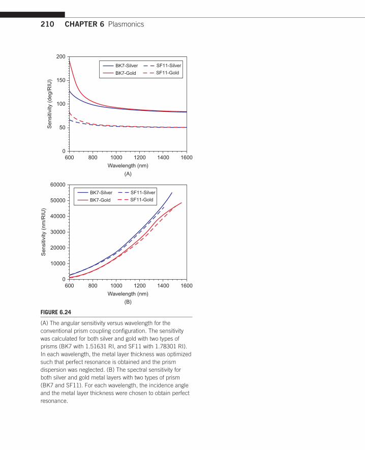
210 CHAPTER 6 Plasmonics
6000
50
100
150
200
BK7-Silver
BK7-Gold
SF11-Silver
SF11-Gold
800 1000
Wavelength (nm)
(A)
(B)
Sen
sitiv
ity (
deg/
RIU
)S
ensi
tivity
(nm
/RIU
)
1200 1400 1600
BK7-Silver
BK7-Gold
SF11-Silver
SF11-Gold
600 800 1000
Wavelength (nm)
1200 1400 16000
10000
20000
30000
40000
50000
60000
FIgURE 6.24
(A) The angular sensitivity versus wavelength for the conventional prism coupling configuration. The sensitivity was calculated for both silver and gold with two types of prisms (BK7 with 1.51631 RI, and SF11 with 1.78301 RI). In each wavelength, the metal layer thickness was optimized such that perfect resonance is obtained and the prism dispersion was neglected. (B) The spectral sensitivity for both silver and gold metal layers with two types of prism (BK7 and SF11). For each wavelength, the incidence angle and the metal layer thickness were chosen to obtain perfect resonance.
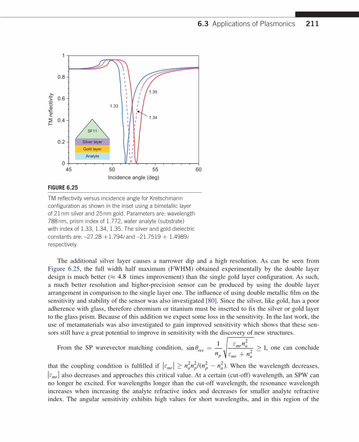
211
The additional silver layer causes a narrower dip and a high resolution. As can be seen from Figure 6.25, the full width half maximum (FWHM) obtained experimentally by the double layer design is much better (≈ 4 8. times improvement) than the single gold layer configuration. As such, a much better resolution and higher-precision sensor can be produced by using the double layer arrangement in comparison to the single layer one. The influence of using double metallic film on the sensitivity and stability of the sensor was also investigated [80]. Since the silver, like gold, has a poor adherence with glass, therefore chromium or titanium must be inserted to fix the silver or gold layer to the glass prism. Because of this addition we expect some loss in the sensitivity. In the last work, the use of metamaterials was also investigated to gain improved sensitivity which shows that these sen-sors still have a great potential to improve in sensitivity with the discovery of new structures.
From the SP wavevector matching condition, sin ,θε
εres
p
mr a
mr an
n
n=
+≥
11
2
2 one can conclude
that the coupling condition is fulfilled if εmr a p p an n n n≥ −2 2 2 2/( ). When the wavelength decreases, εmr also decreases and approaches this critical value. At a certain (cut-off) wavelength, an SPW can no longer be excited. For wavelengths longer than the cut-off wavelength, the resonance wavelength increases when increasing the analyte refractive index and decreases for smaller analyte refractive index. The angular sensitivity exhibits high values for short wavelengths, and in this region of the
0
0.2
0.4
0.6
0.8
1
45 50 55 60
Incidence angle (deg)
TM
ref
lect
ivity
1.35
1.34
1.33
SF11
Silver layer
Gold layer
Analyte
FIgURE 6.25
TM reflectivity versus incidence angle for Kretschmann configuration as shown in the inset using a bimetallic layer of 21 nm silver and 25 nm gold. Parameters are: wavelength 788 nm, prism index of 1.772, water analyte (substrate) with index of 1.33, 1.34, 1.35. The silver and gold dielectric constants are: –27.28 +1.794i and –21.7519 + 1.4989i respectively.
6.3 Applications of Plasmonics

212 CHAPTER 6 Plasmonics
spectrum the sensitivity is governed by a singularity occurring when εmr a p p an n n n= −2 2 2 2/( ). For long wavelengths, the angular sensitivity does not vary considerably with the wavelength. If an angular SPR sensing device operates far from the cut-off, the sensitivity can be approximately expressed as:
Sn n na p a
θθ
≡ =−
d
d
12 2( )
(6.70)
Therefore, the angular sensitivity at high wavelengths depends mainly on the refractive index con-trast between the prism and the analyte and increases with decreasing contrast. Actually the relation-ship between the sensitivity and the prism refractive index does not only exist in the region of high wavelengths, but it is also valid at smaller wavelength. Furthermore, this relationship is valid for spec-tral sensitivity as well as angular sensitivity. This correlation can be seen through the expression of spectral sensitivity and Figure 6.24, in which the sensitivity for two types of prisms is shown.
Sensitivity enhancement of the spectral biosensor by modifying the prism refractive index was also presented [81], showing that sensitivity is modulated by the refractive index of the sensing prism of the spectral SPR biosensors with the same incidence angle. The sensitivity of a spectral SPR bio-sensor with fused silica prism (1.458 refractive index at 589 nm) was 1.6 times higher than that with a BK7 prism (1.517 refractive index at 589 nm) at the same incidence angle 46 2. °. The authors attributed the enhancement in the spectral sensitivity not to the direct influence of the prism refractive index in the expression of the spectral sensitivity, but to the difference in the resonance wavelength obtained. The resonance wavelength for the BK7 prism is smaller than that of the fused silica prism, and since the sensitivity scales monotonically with the operation wavelength the sensitivity will be much higher with smaller prism refractive index. Physically, the authors interpreted the increase in the sensitivity as the increase in the penetration depth of the evanescent field for the prism with the smaller refractive index. Although the penetration depth scales with the operation wavelength [82], the effect of increasing the penetration depth on sensitivity enhancement is still inadequate because in the case that was discussed by Yuk the thickness of the proteins layer is very thin, typically ≤10 nm. Furthermore, increasing the wavelength is accompanied not only by a larger penetration depth, but also by depletion in the field intensity at the interface between the metal and the dielectric. Sensitivity enhancement by modifying the prism refractive index under angular interrogation was also consid-ered. In this paper [83], the role of prism material in sensor design was described both theoretically and experimentally. The analyses were carried out by using three prisms with different refractive indices and the reflection spectra were studied under the angular interrogation mode. The experimen-tal values of angular sensitivity increase from 94 46. deg /RIU to 204 41. deg /RIU on changing the refractive index of the prism from 1.597 to 1.456 without changing the other parameters.
The adverse affects of working with low-refractive-index prisms are relatively low dynamic range of the sensor and a large FWHM of the SPR reflection spectra, which must also be considered before selecting the prism material. The authors did not give an explicit interpretation of the enhancement in the sensitivity due to decreasing the prism refractive index. Overall, the choice of prism material proves to be a vital design parameter and is significant for tuning and optimizing the sensor’s performance.
The addition of a thin dielectric layer with a high refractive index on top of the metal layer is another approach to improve the SPR sensor sensitivity. We emphasize that the added layer is very thin (typically 10 nm) and with high refractive index. One should distinguish this case from the case

213
of coupled plasmon-waveguide resonance (CPWR). CPWR biosensors incorporate a thick waveguide layer (typically 500 nm) beneath the surface of the Kretschmann-based SPR biosensor [84,85]. Unlike the conventional SPR biosensors, whose reflectivity demonstrates a dip only in the TM mode, the interference in the waveguide layer causes a dip both in the TE and TM modes in the CPWR device [86]. Although CPWR sensors exhibit sharp dips and improve significantly the SNR of the measurement, their sensitivity is less than that of conventional SPR devices by an order of magnitude since the biosensing surface is located at a considerable distance from the SPs which exist on the interface between the metal and the waveguide layer [87,88].
The contribution of a thin dielectric top layer to the sensitivity enhancement of SPR sensor was reported for the first time by Lahav et al. [89]. The nearly guided wave SPR (NGWSPR) sensor is similar to the conventional SPR sensor with the addition of a thin Si layer between the metal layer and the cover material to be sensed. The thickness is not thick enough to support a guided mode (see Fig. 6.27). The introduction of a thin ZrO2 layer or other hard dielectrics on top of the silver film for the purpose of protection are possible; however, these layers are usually with smaller index than Si. In the NGWSPR the dielectric layer that was used is Si with thickness of about 10 nm as the refractive index of the silicon is relatively high.
Since the silver has a poor chemical stability, the silicon layer that was added to the sensor pro-tects the metal layer as well as significantly improving its sensitivity. The sensitivity in the NGWSPR case was 4 times larger than the sensitivity of the SPR sensor and 1.5 times larger than the sensitivity when the ZrO2 layer is used. The origin of the enhancement mechanism is in the combination between the SPR phenomenon and the NGWSPR configuration which enables the surface plasmons to spread along the dielectric layer. When the dielectric layer has a large refractive index it can support guided waves for smaller thicknesses. Being thin enough causes a larger fraction of the evanescent field to be in the analyte region. Hence together with the fact that the wave is partially guided (below the cut-off of TM mode), the whole interaction volume is larger, thus increasing the sensitivity. This can be understood from the fact that the sensitivity is related to the overlap integral of the electrical inten-sity in the analyte region which in turn is proportional to the interaction volume [71]. From Figure 6.26 one can see that silicon causes the largest enhancement for the electric field at the interface of the analyte and allows a maximum overlap integral [90].
As mentioned earlier, the surface plasmon can be excited by gratings as well as by prism coupling. By adding a corrugation (grating) to the metal, two things can be accomplished: the grating provides the required momentum matching to the incident light and couples it to the surface plasmons; and sec-ondly, the gratings can perturb the propagation of the surface plasmon. There are two configurations used for grating coupling: direct and indirect. In the direct configuration the light is incident directly onto the metal–dielectric interface from the dielectric side [91], while in the indirect configuration the light is incident through a prism [92,93] (see Fig. 6.27A). The indirect configuration caught the inter-est of many researchers because it allows us to couple light to the surface plasmon by the TIR config-uration and then to perturb it by adding the grating [94,95]. Surface plasmons propagating along the grating vector will experience back reflections. If the period of the grating corresponds to the Bragg condition then a band gap will form where no plasmons are permitted to propagate. Mainly, the band gap is used to control the surface plasmon propagation direction similar to the use of waveguides and photonic crystals in telecommunications. In the context of biosensing, Alleyne et al. [96] showed theoretically that the surface plasmons on the edge of the band gap experience an increased sensitivity to bulk index changes in the dielectric above the grating.
6.3 Applications of Plasmonics

214 CHAPTER 6 Plasmonics
By choosing various gratings with different heights and periods, the authors maintained the band gap to be near the wavelength excitation. By designing the operating point of the sensor to be near the band gap, the sensitivity was improved by a factor of 6 compared with the sensitivity of the conven-tional SPR sensor with flat metallic layer (see Fig. 6.27).
An extinction-based transmission-type SPR sensor is also plausible and has been extensively inves-tigated to study spectral out-coupling of surface plasmons excited in nanostructures often using a wave-length-scanning setup. One of the significant limitations of this coupling is the transmission power efficiency to associate them with other external devices. By using the Kretschmann configuration with a dielectric grating on a silver film, an out-coupling efficiency of 50% was presented and proved experi-mentally by Ref. [97], 68% was obtained by Ref. [98], and theoretically 72% was predicted [99].
Numerical investigation of the transmission-type SPR sensor with dielectric and metallic gratings was performed in Ref. [100]. They showed that a metallic grating has the advantage of narrower transmission peaks and a high sensitivity compared with a dielectric grating but with lower maximum transmittance. A similar comprehensive work was done by Bin et al. [101] in which they investigated transmission-type SPR sensor with metallic dielectric mixed gratings, compared to the conventional dielectric gratings-based structure. It was found that the transmittance efficiency and the FWHM of the transmission curve can be modulated by increasing or decreasing the metallic part. Therefore, the appropriate proportion of the metal
2nd metalinterface
0
Fiel
d in
tens
ity |E
x|2
0
5
10
15
20
25
30
35
40
45
502nd Siinterface
2nd ZrO2interface
SPR
GWSPR
50 100Distance from the prism-metal interface (nm)
150 200
Metal film
Dielectric film
Analyte
θp
250
FIgURE 6.26
Schematic illustration of the NGWSPR configuration. Electric field intensity distribution versus the distance from prism–metal interface for three cases: conventional SPR configuration with no top layer and 43 nm silver layer with 1.33 analyte refractive index, 20 nm thickness of ZrO2 layer with 2.1517 refractive index on the top of 43 nm silver layer and with 1.33 analyte refractive index, 10 nm Si layer on top of 43 nm silver. For the three cases the wavelength is 633 nm and the prism refractive index is 1.73205. (Reproduced from reference [91].)

215
part will induce enhancement factor of the sensor merit (see Fig. 6.28). Furthermore, this structure will also bring enhancement of resonant angle shift, which can be explained by plasmonic interpretation based on a surface-limited increase of interaction area and excitation of localized surface plasmons (LSPs).
The long-range SPR (LRSPR) biosensors based on Kretschmann configuration comprise four basic layers, namely the prism, the dielectric buffer layer, the metal layer, and the analyte. In these devices, the thin metal layer is separated from the prism by an additional dielectric buffer layer [102–105], as shown in Figure 6.5. If the dielectric constant of the dielectric buffer layer is very similar to that of the intended analyte, and is lower than that of the prism, a symmetric environment is achieved on either side of the metal thin film. Ideally the dielectric constants of the dielectric buffer layer and the analyte will be equal, i.e. ε εb a= . If the thickness of the thin metal layer is such that k dzm m⋅ << 1, the resulting symmetric configuration causes the same surface plasmon frequency to exist on both sides of the thin metal layer, and interaction then takes place between the electromagnetic fields of both surfaces.
Silver
P h
t
Substrate:Glass
1
0.8
(A) (B)
(C) (D)
0.6
0.4
0.2
Ref
lect
ivity
Angle of incidence (deg) Sample index
Sen
sitiv
ity ∆
θ/R
IU
0 0
100
200
300
400
500
600
700
60 1.33 1.332 1.334 1.336 1.338 1.3465 70 75 80 85
Flat surface Flat surfaceh = 20 nm
h = 40 nmt = 30 nm
ρ = 300 nm
t = 40 nmρ = 300 nm
t = 40 nmρ = 274 nm
t = 30 nmρ = 270 nm
90
Indirect grating
ATR
t = 50 nmρ = 300 nm t = 50 nm
ρ = 244 nm
FIgURE 6.27
(A) Combined TIR and indirect grating coupled SPR. (B) The surface grating structures. (C) Reflectivity dips for a flat surface and two gratings (both with t = 50 nm) with sample index values from 1.33 to 1.34. The asterisk shows the curve minima (D) sensitivity versus sample index for a flat surface (black solid line) and various gratings. The grey curves represent grating with h = 20 nm and h = 40 nm. The period required to keep the band edge near λ = 850 nm is also noted. (Reproduced from reference [96].)
6.3 Applications of Plasmonics

216 CHAPTER 6 Plasmonics
Following Eq. 6.16, the dispersion relation for + represents the short-range surface plasmon fre-quency while that for − denotes the long-range surface plasmon frequency mode. These modes are characterized by greater and lesser loss, respectively. Compared to the conventional SPR biosensor, the propagation length of the long-range surface plasmon in increased by a factor of approximately 10 times. The incident beam energy is more concentrated, and the depth-to-width ratio of the reso-nance dip is increased. The reflectivity minimum at a lower angle has a smaller half-width and hence indicates the long-range surface plasmon mode, while the dip at a higher angle is indicative of the short-range surface plasmon mode. In Ref. [106] it was shown that for specific combinations of metal thickness and buffer layer thickness, the magnitude of the sensitivity can be extremely high, of the order of 1 105× nm/RIU, when the buffer layer was made of Teflon AF-1600, compared with a sen-sitivity of 1 4 104. × nm/RIU for a conventional prism-coupled wavelength-interrogation SPR sensor
Refractive index of analyte
Res
onan
t pea
k sh
ift (
deg)
1.33
4.0DielectricMetallic-dielectric
3.5
3.0
2.5
2.0
1.5
1.0
0.5
0.0
1.34 1.35 1.36
Incidence angle (deg)30
Tran
smitt
ance
0.0
0.2
0.4
0.6Ag 20nm+PMMA 90nm
Ag10nm+PMMA 100nm
PMMA 110nm
40 50 60 70
ReflectIncident(A) (B)
(D)(C)
BK7 substrate
Ag flim
DielectricgratingsSuperstrate
Transmission
θ T
θ 1
Λ
Ag gratingsdf
dmgddg
1.5
1.3
1.1
0.90 5 10
Height of Ag part (nm)
Enh
ance
men
t fac
tor
15 20 25
FIgURE 6.28
(A) Schematic of metallic–dielectric mixed gratings based SPR structure. (B) Transmittance curves (1T) for air substrate as a function of incidence angle. The grating thickness is fixed at 110 nm with three different proportions between metal and dielectric (110 nm PMMA, 10 nm metal and 100 nm PMMA, 20 nm metal and 90 nm PMMA). (C) Influence of the Ag part on enhancement factor of sensor merit in air substrate. The metal height varies from 0 to 25 nm when the total grating height is fixed at 110 nm. (D) Resonant peak shift of conventional dielectric gratings (110 nm PMMA) in comparison with a dielectric–metallic mixed one with 20 nm Ag and 20 nm PMMA. (Reproduced from reference [101].)
217
operating at 850 nm. In Ref. [107] it was shown that just a slight improvement is achieved in the LRSPR device compared to the conventional SPR configuration with spectral interrogation, and a lesser sensitivity when the angular interrogation is considered. The difference between the last two studies is attributed to the fact that in the latter the authors focused upon the variation in refractive index and thickness of the biomolecular layer, whereas in the former work the researchers considered variations in the refractive index of the buffer layer solution. The wavelength interrogation induces variations in the dielectric constants of the sensor layers (metal layer, buffer layer, analyte) which have a significant effect on the symmetric environment of the LRSPR biosensor. Even though the LRSPR sensor has a slightly higher sensitivity and a much narrower dip than the conventional SPR sen-sors, its requirement of a symmetric configuration is a significant drawback in environmental detec-tion of various biomolecules, and hence tends to restrict its use in practical biosensing applications. By exploiting the very narrow dip in the LRSPR configuration and advanced photonic components Slavik and Homola [108] reported an SPR sensor with very low detection limit (about 2 5 10 8. × − ). Within another experimental study [109], an SPR sensor based on spectroscopy of LSPR for detection of large analytes such as latex beads and bacteria was reported. In the LSPR sensor a spectral sensitiv-ity of 59 000, nm/RIU was measured which is about 8-fold higher than the sensitivity of conventional SPR sensors when the resonance was obtained close to 850 nm.
Under our previous definition of the angular sensitivity, the sensitivity decreases when increas-ing the operation wavelength. In general the performance of any SPR sensor is determined in terms of two aspects. First, the shift in resonance angle ( )δθres for a given change ( )δna in the sensing layer refractive index should be as large as possible. Second, the full width at half-maximum (FWHM) corresponding to the SPR curves ( )δθHM should be as small as possible so that the error in determin-ing the resonance angle is minimal. Taking these aspects into account, many researchers defined a performance parameter called intrinsic sensitivity ( )Si . The parameter ( )Si is directly proportional to the shift in resonance angle ( )δθres and is inversely proportional to the average FWHM ( )δθHM of two SPR curves (see Fig. 6.29). Mathematically, the intrinsic sensitivity of the sensor is:
Si
res
HM
=δθδθ
(6.71)
When adopting the last definition of the sensitivity, the behavior of the sensitivity versus wave-length will take a different form. If we consider that the imaginary parts of the dielectric constants of both the metal and the analyte are not negligible, the plasmon wave vector will include an imaginary part which affects mainly the width of the dip, while the real part determines the position and the shift in the resonant angle. Increasing wavelength reduces the angle shift as well as the dip width. Since the influence of increasing wavelength on the curve width is larger than its influence on the resonance shift, the intrinsic sensitivity was found to be larger in the IR region [110]. Additional def-initions were taken to SPR sensor’s sensitivity; for example in Ref. [111] the sensitivity was defined as the change in the reflectivity per change in the analyte refractive index: ∂ ∂R nTM a/ . Under this definition, maximum sensitivity is achieved at some angle that corresponds to SPR dip with the larg-est slope, where reflectivity sharply drops from unity to almost zero (see Fig. 6.30). However, under the basic concept of sensitivity that is the shift in the incidence angle per change in the analyte refractive index, the sensitivity evidently decreases in the MIR and IR regions comparable to the visible range.
6.3 Applications of Plasmonics

218 CHAPTER 6 Plasmonics
0
0.2
0.4
0.6
0.8
1
48 50 52 54 56 58 60Incidence angle (deg)
Ref
lect
ivity
633 nm, na = 1.325
633 nm, na = 1.335
2000 nm, na = 1.325
2000 nm, na = 1.335
FIgURE 6.30
Reflectivity of SPR sensor in the visible versus the IR range. The reflectivity was calculated at 633 nm and 2000 nm wavelength for two values of the analyte refractive index (1.325, 1.335). The silver layer thickness was optimized to obtain perfect resonance (47 nm at 633 nm wavelength and 25 nm at 2000 nm wavelength); the prism refractive index is 1.732.
0
0.2
0.4
0.6
0.8
1
1.2
53 54 55 56Incidence angle (deg)
Ref
lect
ivity
na = 1.325
na = 1.335
δθres
δθHM
FIgURE 6.29
Illustration of the FWHM ( )δθHM and shifting ( )δθres of two SPR curves in response to slightly different analyte refractive index ( )δna . The prism refractive index is 1.732, wavelength 633 nm, the metal layer is silver with 43 nm thickness and the sensing layer is water with 1.33 RI.

219
The advantages of operating at larger wavelengths according to Ref. [112] are: (1) Penetration depth of the surface plasmon in the visible range is very short. This is beneficial for studying very thin layers, but detrimental for studying cells and cell cultures. The surface plasmon in IR penetrates much deeper and is more appropriate for studying cells. (2) Spectroscopy, since many biomolecules have specific absorption bands in the IR range, performing multi-wavelength SPR measurements allow these biomolecules to be identified selectively. (3) Long-range propagation, the propagation distance of the SP waves is determined by the ratioλε εmr mi
2 / . The propagation length increases extremely in the IR range due to the large ratio between εmr
2 and the imaginary part of the metal dielectric constant ( )εmi , e.g. the propagation length equals 0.154 mm at 633 nm wavelength, and 2.88 mm at 2 m wave-length. Although SPR sensor in the IR region has the advantages above, its angular sensitivity is still smaller than its counterpart in the visible range (assuming the analyte dispersion is negligible) and the multiplicity of the sensitivity definitions is still questionable. However, if the dispersion of the analyte was taken into account, one can exploit the absorption of the sensed media at high wave-lengths to enhance sensitivity. Another experimental study [113] reported significant enhancement in the SPR sensor sensitivity in the mid IR region (about five times greater than in visible) when they detected CO2. They attributed this enhancement to the absorption of CO2 at 4 4. m, which was the operation wavelength in their experiments. While all the previous discussions in this section were on angular sensitivity, one can see in Figure 6.24B that the spectral sensitivity has an opposite behavior from the angular sensitivity. Because the spectral sensitivity is mainly determined by the real part of the metal dielectric constant and the metal dispersion, it increases when increasing wavelength.
Moreover, using a prism with strong normal dispersion d
d
np
λ<
0 may cause an additional contribution
to the sensitivity enhancement in the IR range. A silicon prism was used [114,115] to modify the dispersion relation of the incident light from the ambient in order to improve the sensor performances and miniaturize the structure dimensions.
6.3.1.4 Recent Developments in PSPR SensingDue to the intensive advances in extraordinary optical materials, many researchers’ interest in the excitation of surface plasmons from engineered nano materials, and consequently investigating the effect of such materials on the sensitivity of biosensors, are based on these structures. The use of met-amaterials was proposed recently [116] for plasmon resonance sensors at microwave frequencies. The work deals with a surface plasmon sensor making use of an isotropic and homogeneous metamaterial. However, there are some practical issues, including the questions of how to construct such metama-terials, and what the effects of anisotropic characteristics are. Since most metamaterials are known to be highly dispersive and lossy, the sensitivities need to be carefully studied. It is also important to investigate how to construct practical broadband, low-loss metamaterials. The use of porous materials to the purpose of SPR biosensors has also been under the investigation of many groups. A new design was presented [117] for an optical sensor based on porous silicon (PS) structures. The presented con-figuration contains a low-index (high-porosity) porous silicon layer above the silicon substrate that provides evanescent coupling to a waveguide resonance arising from the high-index (low-porosity) porous silicon resonator layer (see Fig. 6.31). The coupling and resonator layers play the role of metal film in the SPR device. Since the target material can be placed inside the resonator, precisely where the excited resonance fields are the strongest, the scattering losses in PS structures are much less than
6.3 Applications of Plasmonics
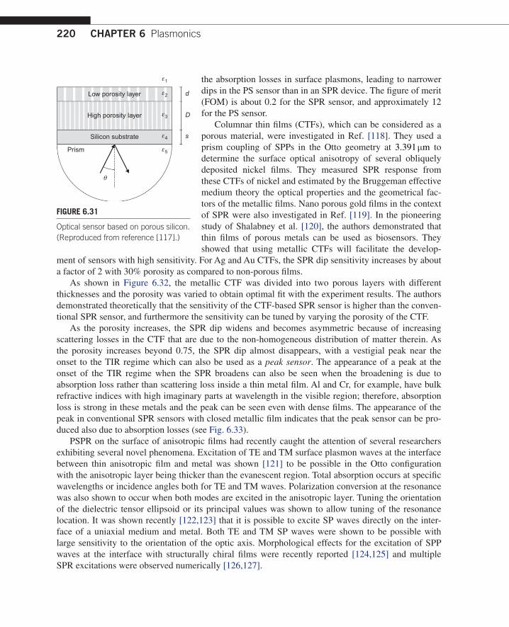
220 CHAPTER 6 Plasmonics
the absorption losses in surface plasmons, leading to narrower dips in the PS sensor than in an SPR device. The figure of merit (FOM) is about 0.2 for the SPR sensor, and approximately 12 for the PS sensor.
Columnar thin films (CTFs), which can be considered as a porous material, were investigated in Ref. [118]. They used a prism coupling of SPPs in the Otto geometry at 3 391. m to determine the surface optical anisotropy of several obliquely deposited nickel films. They measured SPR response from these CTFs of nickel and estimated by the Bruggeman effective medium theory the optical properties and the geometrical fac-tors of the metallic films. Nano porous gold films in the context of SPR were also investigated in Ref. [119]. In the pioneering study of Shalabney et al. [120], the authors demonstrated that thin films of porous metals can be used as biosensors. They showed that using metallic CTFs will facilitate the develop-
ment of sensors with high sensitivity. For Ag and Au CTFs, the SPR dip sensitivity increases by about a factor of 2 with 30% porosity as compared to non-porous films.
As shown in Figure 6.32, the metallic CTF was divided into two porous layers with different thicknesses and the porosity was varied to obtain optimal fit with the experiment results. The authors demonstrated theoretically that the sensitivity of the CTF-based SPR sensor is higher than the conven-tional SPR sensor, and furthermore the sensitivity can be tuned by varying the porosity of the CTF.
As the porosity increases, the SPR dip widens and becomes asymmetric because of increasing scattering losses in the CTF that are due to the non-homogeneous distribution of matter therein. As the porosity increases beyond 0.75, the SPR dip almost disappears, with a vestigial peak near the onset to the TIR regime which can also be used as a peak sensor. The appearance of a peak at the onset of the TIR regime when the SPR broadens can also be seen when the broadening is due to absorption loss rather than scattering loss inside a thin metal film. Al and Cr, for example, have bulk refractive indices with high imaginary parts at wavelength in the visible region; therefore, absorption loss is strong in these metals and the peak can be seen even with dense films. The appearance of the peak in conventional SPR sensors with closed metallic film indicates that the peak sensor can be pro-duced also due to absorption losses (see Fig. 6.33).
PSPR on the surface of anisotropic films had recently caught the attention of several researchers exhibiting several novel phenomena. Excitation of TE and TM surface plasmon waves at the interface between thin anisotropic film and metal was shown [121] to be possible in the Otto configuration with the anisotropic layer being thicker than the evanescent region. Total absorption occurs at specific wavelengths or incidence angles both for TE and TM waves. Polarization conversion at the resonance was also shown to occur when both modes are excited in the anisotropic layer. Tuning the orientation of the dielectric tensor ellipsoid or its principal values was shown to allow tuning of the resonance location. It was shown recently [122,123] that it is possible to excite SP waves directly on the inter-face of a uniaxial medium and metal. Both TE and TM SP waves were shown to be possible with large sensitivity to the orientation of the optic axis. Morphological effects for the excitation of SPP waves at the interface with structurally chiral films were recently reported [124,125] and multiple SPR excitations were observed numerically [126,127].
Low porosity layer
High porosity layer
Silicon substrate s
D
d
Prism ε5
ε4
ε3
ε2
ε1
θ
FIgURE 6.31
Optical sensor based on porous silicon. (Reproduced from reference [117].)

221
6.3.1.5 Sensing with LSPR and Nanostructure DesignThe most common method for LSPR sensing is the wavelength-shift measurement, in which the change in the maximum (or minimum) of the extinction curve is monitored as a function of changes in the local dielectric environment caused by analyte adsorption. This relationship is described in Eq. 6.41, and has been demonstrated for a number of systems in which either the bulk-solvent refractive index or the length of a molecular adsorbate (i.e., a linear alkane chain) is changed. In this equation, the sensitivity to the bulk refractive index ( )S bulkλ− plays an important role in determining the total response of the LSPR. This sensitivity depends on various factors such as size and shape of the nano-particles; in the following section we discuss the effect of the particle’s shape and design on the sens-ing process.
(A) (B)
h
αd
(D)(C) Laser diodeat 653 nm
Lens
BK7prism
Polarizer
Indexmatchingfluid
CTF
Glasssubstrate
Rotationstage
Photodiodewithamplifier
0
Sen
sitiv
ity (
deg/
RIU
)
100
125
150
175
200
225
220
0.05 0.1 0.15
P1 = P2 = 0
P1 = 0P1 = 0.1P1 = 0.2P1 = 0.3
Porosity of 2nd layer0.2 0.25 0.3
Oscilloscope
φ
θ
FIgURE 6.32
(A) Silver columnar thin films (top view). (B) Silver columnar thin film (cross-section). (C) Schematic of the Kretschmann configuration using CTF as the metal film. (D) Simulation results to demonstrate the sensitivity enhancement as the porosity deceases. Calculated sensitivity when the porosity of the first layer (thinner layer) is kept fixed as indicated in the legend while the porosity of the thicker layer is varied from 0 to 0.3. (Reproduced from reference [120].)
6.3 Applications of Plasmonics

222 CHAPTER 6 Plasmonics
Apparently, the resonance position is not dependent on the particle size as can be seen by Eq. 6.46 for a sphere and Eq. 6.48 for arbitrary smooth particle and only variation in the intensity of SPR band with particle size is observed. However, experimentally the SPR bandwidth as well as band posi-tion is observed to depend on the nanoparticle size. In the modification to the Mie theory, Drude and Sommerfeld considered that the relative permittivity of the nanoparticle depends on the size ε ( , )R in lieu of ε ( ). The real and the imaginary parts of the modified relative permittivity are given by [128,129]:
ε ε
′ ( ) = −
+ib
p
d
2
2 2 (6.72)
and
ε
″ ( )
( )=
⋅
+p d
d
2
2 2 (6.73)
where εib is the high-frequency limit of ε ( ), arising from response of the core electrons (electrons in completely filled bands); d is the relaxation or damping frequency which represents collisions of electrons with the lattice (phonons) and defects; and p is the bulk plasmon frequency. The depend-ence of the relative permittivity on the particle radius R was introduced by assuming that the particle
1
Simulationair
Simulationwater
Experimentair
Airsimulation
AirExperimentWaterExperiment
Watersimulation
Experimentwater
0.9
0.8
Ref
lect
ance
for
p-po
lariz
atio
n
0.7
0.6
0.5
0.4
0.3
0.2
0.1
020 30 40 50 60 70 80
φ (deg)
90
FIgURE 6.33
Measured/simulated data for p-polarization reflectance R versus the angle φ when the dense/non-porous (p = 0) metal film is 8 nm thick and made of Cr. The curves exhibit a broad dip and a sharp and symmetric peak due to the absorption in bulk Cr. The analyte sensed is either air or water (refractive index = 1.33). (This graph is reproduced from reference [120].)
223
size is smaller than the mean free path of conduction electrons. The damping frequency d is related to the mean free path of conduction electrons in bulk metal Rbulk and Fermi velocity of electrons v f by:
d
f
bulk
v
R=
(6.74)
When R becomes smaller than the mean free path, surface scattering is dominant. This surface scattering results in the peak broadening and induces a 1/R dependence of the SPR bandwidth. In this case, the mean free path Reff becomes size-dependent according to:
1 1 1
R R Reff bulk
= + (6.75)
One can see from Eqs. 6.47–6.49 that the metal particle’s shape dictates the spectral signature of its plasmon resonance; the ability to change this parameter and study the effect on LSPR response is a very important experimental challenge. The development of increasingly sophisticated lithographic and chemical methods now allows the routine production of a wide variety of complex NPs and their assemblies [130].
In contrast to the size of the nanoparticle, a change in shape produces larger shifts and modification in the LSPR band. In a theoretical study of the LSPR bulk sensitivity behavior, which was presented in Ref. [131], the authors used the discrete dipole approximation (DDA) to calculate the electrody-namic response of an arbitrary nanoparticle to a plane wave excitation. By investigating the correlation between the extinction spectra of the particle and the aspect ratio, material properties, and resonance wavelength, interesting results were obtained. The resonance wavelength increases with increasing aspect ratio [132,133], and the sensitivity has a positive correlation with the resonance wavelength. The calculations were fitted with analytical approximations which demonstrated that bulk sensitivity was basically dependent on resonance wavelength, particle material dispersion, and the medium refrac-tive index. Figure 6.34 demonstrates the correlation between resonance wavelengths for cylinders, discs, and hallow nanoshells made from gold with various aspect ratios. Figure 6.34D shows the linear dependence of the bulk sensitivity on the resonance wavelength. The nanotriangles of Ag synthesized using nanosphere lithography (NSL) were used [134] as an LSPR biosensor that monitors the interac-tion between a biotinylated surface and free streptavidin or anti-biotin in solution. LSPR sensor for detection of Salmonella bacteria was demonstrated [135] showing that due to the small contact area between the nanoparticle and the bacteria and the short-range interaction of the local electric field, the plasmon peak shift induced by such a system is about 2–4 nm, regardless of the concentration of the bacteria. A multireflections-based device was used in Ref. [136] to study the LSPR response of gold nanoparticles on a glass substrate to changes in sucrose concentration as an analyte. The authors found that multireflections of the incident beam at the glass–nanoparticles interface improve the sensitivity of the detection process.
In addition to the effects of the medium, the dependence of the nanoparticle surface plasmon reso-nance on the interaction between proximal nanoparticles has also been studied in detail [137,138]. When noble metal nanoparticles come in close proximity, the plasmon resonance oscillations on the individual nanoparticles are coupled. For light polarized parallel to the interparticle axis, this coupling
6.3 Applications of Plasmonics

224 CHAPTER 6 Plasmonics
results in a red shift in the plasmon resonance, which increases with decreasing interparticle separa-tion. A pair of gold nanospheres was used [139] as a model coupled-particle system for investigating the effect of the separation distance between the particles on the LSPR response.
Similar to isolated nanoparticles, Figure 6.35 shows that for coupled nanoparticle pairs there is a red shift in the plasmon resonance of the two-particle system as the medium refractive index is increased. The rate at which the plasmon resonance red shifts in response to a given refractive index change increases rapidly as the interparticle separation in the nanosphere pair is decreased. The
500
Sca
tterin
g ef
ficie
ncy
Sca
tterin
g ef
ficie
ncy
0
1
2
3
4
5
6
8(A) (B)
(C) (D)
6
4
2
0
Sca
tterin
g ef
ficie
ncy
20
15
10
5
0
∆λ*/
∆n
0
100
200
300
400
500
600
550 600 650Wavelength (nm)
700 750 800 500
650600 700 800 700 750 800
550 600 650Peak wavelength (λ*)
Wavelength (nm)Wavelength (nm)
700 750 800
FIgURE 6.34
(A) Scattering spectra of gold nanocylinders in media of refractive index 1.33 (thick lines) and 1.41 (thin lines). Cylinders are 20 nm in diameter and 40 (solid lines), 50 (dashed lines) or 60 (dotted lines) nm in length. (B) Scattering spectra of gold nanodiscs in media of refractive index 1.33 (thick lines) and 1.41 (thin lines). Discs are 12 nm in height and 60 (solid lines), 80 (dashed lines) or 100 (dotted lines) nm in diameter. (C) Scattering plasmon bands of three hollow gold nanoshells in media of refractive index 1.33 (thick lines) and n = 1.41 (thin lines). The particles have core radii of 5 (solid lines), 30 (dashed lines) and 50 nm (dotted lines) and 15 nm thick gold shells. Note that sensitivities are calculated under the assumption that the refractive index of the interior, ncore, varies identically with that of the external medium. (D) Sensitivity of scattering LSP peak wavelength to bulk refractive index as a function of peak wavelength. Sensitivities of gold nanodiscs (open squares), nanocylinders (dashes) and hollow nanoshells (open circles) of size parameters less than 0.77 are shown. (Reproduced from reference [131].)

225
sensitivity was found to be very strongly dependent on the separation between the coupled particles as can be seen from Figure 6.35, where D in Figure 6.36 is the particle diameter and d is the interparticle surface- to-surface separation.
A wide variety of nanoparticle shapes were pro-posed as an LSPR sensor, like rings [140], dots [141], stars [142], nanobottles [143] and many other shapes. A very important aspect in shape modification is the field enhancement associated with the structure design. As mentioned before, the field enhancement in the vicin-ity of the nanoparticles plays a very significant role in improving sensitivity when this structure is used as a biosensor and this phenomenon has a key application in surface-enhanced spectroscopy like surface-enhanced Raman scattering (SERS) and surface-enhanced fluor-escence (SEF). When the nanostructure has more cor-ners, more resonance wavelengths can be excited and more hot spots can be obtained at these resonance wavelengths. In U-shaped structures that were pre-sented [144], more resonance wavelengths in the visible range were excited compared to parallel nanorods. The electrons in the parallel nanorod structure can oscillate
630(A) (B)
600
570
60
40
20
0
540
510
1.0
90 nmInter-particle separation
65 nm40 nm25 nm10 nm6 nm4 nm
1.1 1.2
Refractive index
Pla
smon
res
onan
cem
axim
um (
nm)
1.3 1.4 1.5 1.6 1.0 1.1 1.2Refractive index
Pla
smon
shi
ft (n
m)
1.3 1.4 1.5 1.6
FIgURE 6.35
(A) Plasmon resonance wavelength maximum and (B) coupling-induced resonance wavelength red shift for a pair of 40 nm gold nanospheres as a function of the medium refractive index for different interparticle separations. The plasmon resonances were simulated for light polarized along the interparticle axis. The solid lines are straight-line fits. (Reproduced from reference [139].)
180
160
140
120
100
80
Sen
sitiv
ity (
nm/R
IU)
0.0 0.5 1.0 1.5 2.0 2.5
s/D
FIgURE 6.36
Plasmon resonance sensitivity ( )∆ ∆λSP mn/ in the gold nanosphere pair plotted as a function of the interparticle separation in units of the particle diameter s D/ . The sensitivity increases near exponentially with decreasing s D/ as seen from the fit (solid line) to the single-exponential decay ( exp( ))y y a x= + ⋅ −0 /τ where τ = ±0 18 0 04. . . The error bars represent the error in the straight line fits in Figure 6.24A. (Reproduced from reference [139].)
6.3 Applications of Plasmonics

226 CHAPTER 6 Plasmonics
within the individual nanorods, while in the U-shaped structure the bottom rod builds a path to connect the two vertical nanorods, and further plasmons can be excited.
As one can see from Figure 6.37, for a parallel nanorod structure just two resonance wavelengths can be excited (at 0 359. m and 0 341. m), while in the U-shaped structure an additional three wave-lengths appear (at 0 820. m, 0 579. m and 0 485. m). When illuminating the U-shaped nanostructure
Ek
Ek
(b) λP = 0.579 µm
(a) λTDM = 0.359 µm
1
2
3
4
5
2
3
4
5
6Ek
(a) λP = 0.820 µm
3
4
5
6
5
(A) (B)
(C) (D)
4
3
2
Qex
t
1
00.4 0.6
l = 2
l = 1Ek
l = 3
Wavelength λ (µm)0.8 1.0
uλTQM
uλTDM
c
FIgURE 6.37
(A) Calculated extinction spectra of the U-shaped nanostructure. (B) E field enhancement contours (log )10 γ of the parallel-nanorod structure at wavelength λ = 0 359. m, a characteristic resonance wavelength to parallel nanorods. (C) E field enhancement contours log10 γ( ) of the U-shaped structure at wavelength λ = 0 820. m, a
resonance wavelength that excited in the U-shaped structure. (D) E field enhancement contours (log )10 γ of the U-shaped structure at wavelengthλ = 0 579. m, a resonance wavelength that excited in the U-shaped structure. (Reproduced from reference [144].)

227
with these wavelengths, a larger enhancement to the local field and more hot spots are obtained. The local field enhancement is expressed by γ ≡ E E
20
2/ , where E is the local electric field and E0 is
the incident field. The resonances can be tuned by controlling the dimensions of the nanostructures, which makes it a very useful tool in biosensing and enhanced spectroscopy.
6.3.1.6 Surface-Enhanced SpectroscopiesThe interaction between light and nanoparticles causes other optical signals to be enhanced such as surface-enhanced Raman scattering (SERS) and surface-enhanced fluorescence (SEF). SERS is a very sensitive spectroscopy that allows the detection of organic molecules adsorbed on noble metal sub-strates (silver, gold, copper) at sub-micromolar concentration. Vibrational Raman spectra from single hemoglobin molecules attached to 100-nm-sized immobilized Ag particles [145]. Since SERS depends strongly on the local field to the fourth power ( E
4dependence) in the vicinity of an adsorbate mol-
ecule [146,147] to the surface, one can significantly enhance the SERS intensity by enhancing the field near the scattering molecules. It was found [148] that by engineering the nanoparticle structure size and shape to yield resonance wavelength that suitably located between the exciting laser and the Raman frequency, one can obtain large enhancement factors of Raman scattering signals. The effects of the nanostructure features (substrate material, nanoparticle material, nanoparticle size, nanoparticle shape, etc.) on the SERS enhancement were intensively investigated during the last few years [149–151]. In Ref. [152] it was shown that a surface plasma wave (SPW), propagating along a metal surface, embedded with regularly arranged nanoparticles, undergoes surface-enhanced Raman scattering from molecules adsorbed over the particles. A significant scattered wave is detected if a relative relationship between the particle arrangement period, Raman frequency and the surface plasmon wave is satisfied. In Figure 6.38, the effects of the temperature and the substrate rotation during the deposition on SERS spectra are demonstrated.
The potential of SEF was rediscovered during the past decade due to the emerging developments in the optics of metallic nanostructures [153]. SEF is a very useful phenomenon with significant applications in biotechnology and life sciences [154]. Localization of the electromagnetic field near nanotips, corners, holes, needles, etc. has been shown to produce large SEF by factors of up to a few hundreds in what is known as the lightning nanoantenna effect [36].
Surface-enhanced fluorescence from porous, metallic sculptured thin films (STFs) was demon-strated for sensing of bacteria in water by Abdulhalim et al. [155]. Enhancement factors larger than 15 were observed using STFs made of silver and aluminum with respect to their dense film coun-terparts. The STFs used are assemblies of tilted, shaped, parallel nanowires prepared with several variants of the oblique-angle-deposition technique (OAD). They examined the effect of the substrate material, constituent rod material, porosity, and the rod tilt angle on the enhancement factor of SEF. Enhancement of SEF from porous, metallic STFs was applied to biosensing in water. The main SEF mechanisms, according to the authors, are believed to be the lightning nanoantenna effect and the dipole–dipole interaction. This observation makes STFs potential candidates as SEF nanobeds for biosensing and bioimaging. In Figure 6.39, one can see the advantage of such sculptured films on their counterpart closed and flat films.
6.3.1.7 Sensing with EotOne of the heavily investigated types of optical sensing mechanisms these days is based on enhanced optical transmission (EOT) through nanoapertured metallic thin films. These structures are planar and
6.3 Applications of Plasmonics

228 CHAPTER 6 Plasmonics
operating at normal incidence, thus the possibility of producing and operating them in large arrays to provide what is called a biochip. The EOT phenomenon is based on localized surface plasmon reso-nances (LSPRs) excited at the surface of the nanoapertures [156,157], although there is some debate on whether the SP wave is localized or propagating in the EOT case [158]. The sensing mechanism is based on the existence of evanescent field inside the analyte which is affected by the variation of the refractive index of the analyte. A comparative study was performed [159,160], which verifies higher sensitivity of nanoslits over nanohole-based structures and therefore nanoslits are better candidates for sensing designs. Hence the sensitivity depends on the strength of this field and on its extent within the analyte, called the penetration depth. Since with LSPR phenomena the field is enhanced strongly in the nm vicinity of the nanofeature, the sensitivity of LSPR-based sensors has been shown recently [161] to exceed that of extended SPR sensors when the index variations are occurring only in the nm vicinity of the nanofeature. To detect bulk variations in the analyte and pollutants with few microns size such as bacteria, the deep penetration of the field in the analyte is important; however, the sensitivity in this case is lower than the case of extended SPR sensors. In the visible range of the spectrum the enhanced
18000
10000
20000
30000
40000
50000
60000
1500Raman shift (cm−1)
Ram
an in
tens
ity (
arb.
uni
t)
1200 900 60016
4815
7515
11
1361
1311
1180
774
612
1(d)
1(c)
1(b)1(a)
500 nm 500 nm
500 nm 500 nm
1(d)1(c)
1000
2000
3000
4000
5000
6000
Ram
an in
tens
ity (
arb.
uni
t)
1800 1500Raman shift (cm−1)
1200 900 600
1648
1575
1511 13
6113
11
1180
774 61
2
1(b)
1(a)
(A)
(B)
FIgURE 6.38
Growth morphology of Ag thin films by GLAD at various conditions: (1a) at 120°C without substrate rotation; (1b) at 120°C and substrate rotation at 0.2 rpm; (1c) at −40°C without substrate rotation; (1d) at −40°C and substrate rotation at 0.2 rpm. (A) Raman spectra of R6G on Ag thin films consisting of (a) joined nanorods shown by Figures 7.1A and 1B, and (b) separated Ag nanorods shown by Figures 7.1C and 7.1D, respectively, at a concentration of 1 10 6× − mol/L. (Reproduced from reference [149].)

229
local field extends only to a range of about 50–100 nm inside the analyte; hence it will not sense the whole volume of a bacteria cell for example. This problem is well known in the traditional prism-coupled SPR sensors even though extended SP waves have a relatively larger propagation length along the surface of the order of 1m [162]. Long-range SPR configurations were proposed [163] to resolve this problem. Sensors based on EOT strongly depend on the detailed structure of the nanomaterial. It is well known that the aperture size and type of the metallic nanostructures have different contributions to the extraordinary transmission [164–167].
To describe the concept we focus on the case of a one-dimensional (1D) periodic array of nanoslits, although the same idea applies to other periodic structures in metals such as a 2D array of nanoholes. Figure 6.40A shows the general 1D structure and the geometrical parameters. When the nanoslit structure is irradiated by TM polarized light at normal incidence one obtains resonant transmission peaks as shown in Figure 6.40B. The resonance wavelength is found from the k-vector matching condition of SPR exist-ence, k kx sp= , which at normal incidence and first-order diffracted wave gives:
λε εε εSP
m a
m a
≈+
Re (6.76)
where ε ε εm mr mii= + is the metal dielectric constant and εa is the dielectric constant of the analyte. Equation 6.76 is valid for the first resonance peak and for thick metal film; however, it is used as well for estimating the SPR location for thin metal films as the thickness of the metal film has negligible effect on the k-vector of the plasmon.
The sensitivity of the sensor is measured in nm per refractive index units (nm/RIU), defined [168] as the slope of the variation λSP with the analyte index na a= ε , and can be derived from Eq. 6.76:
Ssp
a
m
m a SPa
m
mSP
m
a
a=
+ −∂∂−
∂∂
λ
ε
ε
ε ε λεεελ
λεεελ
Re( ) . .0 5 0 5
(6.77)
(A) (B)
500
400
300
200
100
0550 600 650
Wavelength (nm)
Sig
nal (
coun
ts)
700 750 800 850
Ag
(C) 200 nm
Ag-Ref
Ag-STF
AI-RefAI
FIgURE 6.39
Fluorescence images from (A) Ag nanorod STF and (B) a dense Ag film immersed in an aqueous solution of luminescent E. coli. (C) Typical SEF spectra from an Ag-nanorod STF and an Al-nanorod STF and from the corresponding reference films. Inset: SEM micrograph of an Ag nanorod STF showing the highest enhancement factor. (Reproduced from reference [155].)
6.3 Applications of Plasmonics
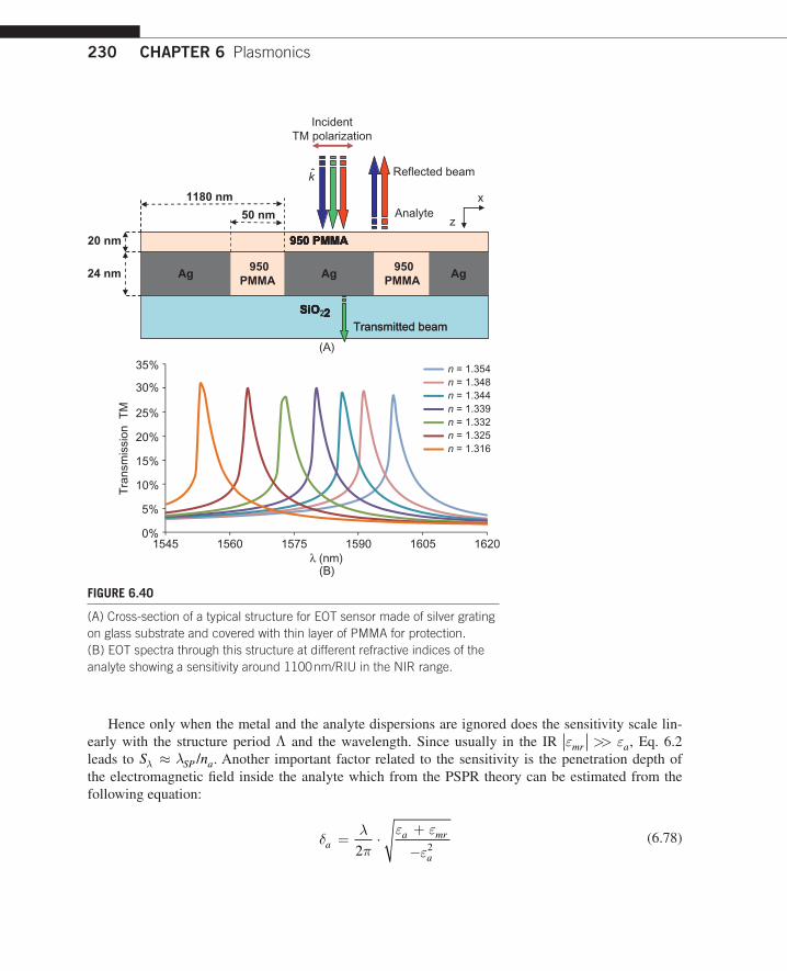
230 CHAPTER 6 Plasmonics
Hence only when the metal and the analyte dispersions are ignored does the sensitivity scale lin-early with the structure period and the wavelength. Since usually in the IR ε εmr a>> , Eq. 6.2 leads to S nSP aλ λ≈ / . Another important factor related to the sensitivity is the penetration depth of the electromagnetic field inside the analyte which from the PSPR theory can be estimated from the following equation:
δλπ
ε ε
εa
a mr
a
= ⋅+
−2 2 (6.78)
SiO 2
950 PMMA
1180 nm
50 nm
k
IncidentTM polarization
Transmitted beam
Reflected beam
(A)
x
zAnalyte
SiO 2
950 PMMA
SiO 2
950 PMMA20 nm
24 nm
SiO 2
950 PMMA
SiO2
Ag Ag Ag
950 PMMA
950PMMA
950PMMA
Transmitted beam
0%
5%
10%
15%
20%
25%
30%
35%
1545 1560 1575 1590 1605 1620
Tra
nsm
issi
on T
M
λ (nm)
n = 1.354n = 1.348n = 1.344n = 1.339n = 1.332n = 1.325n = 1.316
(B)
FIgURE 6.40
(A) Cross-section of a typical structure for EOT sensor made of silver grating on glass substrate and covered with thin layer of PMMA for protection. (B) EOT spectra through this structure at different refractive indices of the analyte showing a sensitivity around 1100 nm/RIU in the NIR range.

231
For example, for silver at λ = 1550 nm we have εmr =−115 5. which is much larger than εa = 1 769. , thus giving a penetration depth of about δ λa = ≈0 96 1 48. . m. For the visible range, λ= 600 nm, on the other hand we have εmr =−14 14. , thus giving δ λa = ≈0 316 0 19. . m. Hence the pen-etration depth in the near IR (NIR) range is larger by a factor of 8 than that in the visible range, although the wavelength ratio is only 2.5. The reason for that is the difference in the real part of the metal dielectric function. Hence larger sensitiv-ities can be obtained by designing EOT sensors with resonances in the infrared range. Figure 6.41 shows the sensitiv-ity and wavelength versus the pitch of the grating over a wide range of wave-lengths. Experimental demonstration for water pollution sensing was presented by
Karabchevsky et al. [169,170] in the visible range of the spectrum.
6.3.2 Light Concentration and PhotovoltaicsOne of the important and emerging nanophotonic applications of plasmonic structures is in enhancing the efficiency of solar cells. As is well known, a major limitation in all thin-film solar cell technolo-gies is that their absorbance of near-bandgap light is ineffective, in particular for the indirect-band-gap semiconductor silicon. Therefore, designing a new structured solar cell that can trap light inside in order to increase the absorptance is very important. For example, light trapping is possible to achieve by forming a wavelength-scale texture on the substrate and then depositing the thin-film solar cell on top, increasing the photocurrent [171]. Metallic nanostructures on top of the semiconductor solar cell can serve this purpose for the same reason of trapping due to scattering but also due to the local field enhancement associated with plasmon excitation. In a pioneering work [172] it was shown that an enhancement in the photocurrent of a factor of 18 could be achieved for a 165-nm-thick silicon-on-insulator photo-detector at a wavelength of 800 nm using silver nanoparticles on the surface of the device. Metal nanoparticles were also shown [173] to increase the efficiency of light-emitting diodes by a factor of 7 for thin silicon-on-insulator light-emitting diodes. Following these works sev-eral researchers started to use metallic nanoparticles to enhance the efficiency of solar cells. In Ref. [174], they obtained 80% enhancement by depositing gold nanoparticles on highly doped wafer-based solar cells, at wavelengths around 500 nm. Conversion efficiency enhancement of 8% was observed [175] using gold nanoparticles on thin-film amorphous silicon solar cells. Silver nanoparticles depos-ited on 1.25-m-thick silicon-on-insulator solar cells and planar wafer-based cells gave overall
0
5
10
15
20
25
0 5 10 15 20Pitch (µm)
Sen
sitiv
ity o
r w
avel
engt
h
λ-first resonance (µm)
Sensitivity (µm/RIU)
FIgURE 6.41
Simulated sensitivity () and resonance wavelengths () versus the pitch of the same structure shown in Figure 6.40A.
6.3 Applications of Plasmonics

232 CHAPTER 6 Plasmonics
photocurrent increases of 33% and 19% respectively [176]. Enhancement in other types of solar cells was also reported [177–180].
In order to understand the origin of the enhancement and design optimum nanostructures rigorous electromagnetic calculations are required to show the contribution of each of the two main mecha-nisms: light trapping and enhanced plasmonic absorption. Light trapping and concentration are per-haps two related phenomena and both play a role in solar cell efficiency enhancement. For spherical metal nanoparticles on substrates with high index it was shown that the scattering takes place mostly in the direction of the substrate. The topic is under extensive investigation by many research groups and several review articles have already been published [181–183].
6.4 FUTURE DIRECTIONSAccording to the number of papers being published and their multidisciplinary nature in the field of plasmonics, it is expected that the field will have a huge impact on our daily life in several aspects: (i) highly sensitive miniature biosensors in array configuration acting as lab-on-chip for point health-care applications, environmental monitoring, food safety and security from dangerous hazards; (ii) solar cells with enhanced efficiency, thus lowering the cost of solar cells, an important factor in taking decisions by governments as whether to go solar or not; (ii) improved photonic devices such as modulators, detectors, tunable filter, and photonic circuits using long-range surface plasmons; (iii) super-resolved imaging useful for molecular imaging and nanolithography; (iv) cancer treatment with metal nanoparticles based on local heating; (v) light concentration for solar cells, scanning opti-cal microscopy and non-linear optical applications; and (vi) data transfer in nanowires since plas-mons can carry the information in metal nanowires, integrating them into nanoelectronic circuits, they can bring to us high capacity of information transfer. In this sense plasmon waves behave on metals much like light waves behave in glass, meaning that the future “plasmonic engineers” can employ all the same ingenious tricks such as multiplexing or sending multiple waves that photonic engineers use to cram more data down a cable. The potential of plasmonics right now is mainly limited by the fact that plasmons typically can travel only several millimeters before they get absorbed. Chips, meanwhile, are typically about a centimeter across, so plasmons are unable yet to go the whole dis-tance. Improvement of the traveling distance of long-range plasmons is a challenge perhaps using new designs or more pure metals or metallic alloys with the correct properties.
The design problem of metal nanostructures is now resolved using robust commercially available electromagnetic simulation software in three dimensions. Hence more complex designs with advanced functionality will emerge in the future. As an example the use of metamaterials near the plasmon reso-nance is essential for devices at visible frequencies. The flexibility in the design of metamaterials may point towards the possible use of composite structures for plasmonic applications. Another blossoming area is quantum plasmonics, which emerges in the limit of closely coupled metallic structures.
In applications in the biofield there is a need for more work on biofunctionalization of metallic nanoparticles and nanostructures for the specific sensing application. Protection from environments that cause oxidation is also needed without deteriorating the plasmonic properties. For structures that will go inside the body, biocompatibility is needed for long-term use.
The manufacturability of these structures is becoming mature in different ways such as chemical means, nanolithography, direct writing and deposition of thin films. All this combined with the explosion

233
of information technology, computing power, miniature detection devices such as spectrometers, cam-eras and lenses is expected to bring a true revolution in the photonics industry. For example, miniature Raman spectrometers are available today at a reasonable price which when combined with nanostruc-tures to obtain high SERS signals can provide a powerful tool for monitoring and sensing. Although research is still required in the field it is ongoing extensively, the time is approaching for the photon-ics industry to start commercializing products based on plasmonic devices. This will help researchers become exposed to true plasmonic industrial problems, which by the end will help the industry itself in a feedback loop fashion.
References [1] H. Raether, Surface Plasmons on Smooth and Rough Surfaces and on Gratings, Springer Verlag, 1988. [2] E. Ozbay, Plasmonics: merging photonics and electronics at nanoscale dimensions, Science 311 (2006)
189–193. [3] M. Born, E. Wolf, Principles of Optics, sixth ed., Pergamon Press, 1986, pp. 51–66. [4] A. Shalabney, I. Abdulhalim, Electromagnetic fields distribution in multilayer thin film structures and the
origin of sensitivity enhancement in surface plasmon resonance sensors, Sens. Actuators A 159 (2010) 24–32.
[5] J.D. Jackson, Classical Electrodynamics, third ed., Academic Press, 1998. [6] U. Kreibig, M. Vollmer, Optical Properties of Metal Clusters, Springer, Berlin, 1995. [7] N.G. Khlebtsov, Optics and biophotonics of nanoparticles with a plasmon resonance, Quantum Electronics
38 (6) (2008) 504–529. [8] H.C. Van de Hulst, Light Scattering by Small Particles, Dover, New York, 1981. [9] W.T Doyle, Absorption of light by colloids in alkali halide crystals, Phys. Rev. 111 (1958) 1067–1072. [10] R.H. Doremus, Optical properties of small gold particles, J. Chem. Phys. 40 (1964) 2389. [11] H. Romer, C. von Fragstein, Z. Physik 163 (1961) 27. [12] U. Kreibig, M. Vollmer, Optical Properties of Metal Clusters, Springer-Verlag, Berlin, 1995. [13] W.T. Doyle, A. Agarwal, J. Opt. Soc. Am. 55 (1965) 305. [14] W.T. Doyle, Phys. Rev. B 39 (1989) 9852. [15] J.M. Pitarke, V.M. Silkin, E.V. Chulkov, P.M. Echenique, Theory of surface plasmons and surface-plasmon
polaritons, Rept. Prog. Phys. 70 (2007) 1–87. [16] A.V. Zayats, I.I. Smolyaninov, A.A. Maradudin, Nano-optics of surface plasmon polaritons, Phys. Rep. 408
(2005) 131–314. [17] J.M. Montgomery, T.W. Lee, S.K. Gray, Theory and modeling of light interactions with metallic nanostruc-
tures, J. Phys.: Condens. Matter 20 (2008) 323201 (11pp). [18] E. Fort, S. Gresillon, Surface enhanced fluorescence, J. Phys. D: Appl. Phys. 41 (2008) 13001 (31pp). [19] E.C. Stoner, The Demagnetizing Factors for Ellipsoid, vol. 36, 1945, No. 263.[20] V.M. Shalaev, Nonlinear Optics of Random Media, Springer, Berlin, Germany, 2000. [21] D.A. Genov, A.K. Sarychev, V.M. Shalaev, A. Wei, Resonant field enhancements from metal nanoparticle
arrays, Nano Lett. 4 (2004) 153–158. [22] T.M. Cotton, J.-H. Kim, G.D. Chumanov, Application of surface-enhanced Raman spectroscopy to biologi-
cal systems, J. Raman Spectroscopy 22 (2005) 729–742. [23] G.C. Schatz, R.P. Van Duyne, Electromagnetic mechanism of surface-enhanced spectroscopy, in:
M.J. Chalmers, P.R. Griffiths (Eds.), Handbook of Vibrational Spectroscopy, Wiley, Chichester, UK, 2002. [24] R.R. Chance, A. Prock, R. Silbey, Molecular fluorescence and energy transfer near interfaces, Adv. Chem.
Phys. 37 (1978) 1–65.
References

234 CHAPTER 6 Plasmonics
[25] K. Aslan, I. Gryczynski, J. Malicka, E. Malveeva, J.R. Lakowics, C.D. Geddes, Metal-enhanced fluores-cence: an emerging tool in biotechnology, Curr. Opin. Biotechnol. 16 (2005) 55–62.
[26] E. Fort, S. Gresillon, Surface enhanced fluorescence, J. Phys. D: Appl. Phys. 41 (2008) 013001. [27] J.R. Lakowicz, Y. Shen, S. D’Auria, J. Malicka, J. Fang, Z. Gryczynski, et al., Radiative decay engineering.
2. Effects of silver island films on fluorescence intensity, lifetimes, and resonance energy transfer, Anal. Biochem. 301 (2002) 261–277.
[28] E.M. Goldys, A. Barnett, F. Xie, K.D. Tomsia, I. Gryczynski, E.G. Matveeva, et al., Plasmon-enhanced fluorescence near metallic nanostructures: biochemical applications, Appl. Phys. A 89 (2007) 265–271.
[29] Y. Zhang, K. Aslan, M.J.R. Previte, C.D. Geddes, Metal-enhanced fluorescence from copper substrates, Appl. Phys. Lett. 90 (2007) 173116.
[30] J. Zhang, J. Malicka, I. Gryczynski, J.R. Lakowicz, Surface-enhanced fluorescence of fluorescein-labeled oligonucleotides capped on silver nanoparticles, J. Phys. Chem. B 109 (2005) 7643–7648.
[31] F. Xie, M.S. Baker, E.M. Goldys, Homogeneous silver-coated nanoparticle substrates for enhanced fluores-cence detection, J. Phys. Chem. B 110 (2006) 23085–23091.
[32] E. Matveeva, Z. Gryczynski, J. Malicka, I. Gryczynski, J.R. Lakowicz, Metal-enhanced fluorescence immunoassays using total internal reflection and silver island-coated surfaces, Anal. Biochem. 334 (2004) 303–311.
[33] J.H. Song, T. Atay, S. Shi, H. Urabe, A.V. Nurmikko, Large enhancement of fluorescence efficiency from CdSe/ZnS quantum dots induced by resonant coupling to spatially controlled surface plasmons, Nano Lett. 5 (2005) 1557–1561.
[34] F. Tam, G.P. Goodrich, B.R. Johnson, N.J. Halas, Plasmonic enhancement of molecular fluorescence, Nano Lett. 7 (2007) 496–501.
[35] T. Liebermann, W. Knoll, Surface plasmon field-enhanced fluorescence spectroscopy, Colloid Surf. A 171 (2000) 115–130.
[36] M. Moskovits, Surface-enhanced spectroscopy, Rev. Mod. Phys. 57 (1985) 783–826. [37] I.-Y.S. Lee, H. Suzuki, K. Ito, Y. Yasuda, Surface-enhanced fluorescence and reverse saturable absorption
on silver nanoparticles, J. Phys. Chem. B 108 (2004) 19368–19372. [38] J.R. Lakowicz, Radiative decay engineering: biophysical and biomedical applications, Anal. Biochem. 298
(2001) 1–24. [39] J.R. Lakowicz, Y. Shen, S. D’Auria, J. Malicka, J. Fang, Z. Gryczynski, et al., Radiative decay engineering.
2. Effects of silver island films on fluorescence intensity, lifetimes, and resonance energy transfer, Anal. Biochem. 301 (2002) 261–277.
[40] J.R. Lakowicz, Y. Shen, Z. Gryczynski, S. D’Auria, I. Gryczynski, Intrinsic fluorescence from DNA can be enhanced by metallic particles, Biochem. Biophys. Res. Commun. 286 (2001) 875–879.
[41] I. Gryczynski, J. Malicka, Y. Shen, Z. Gryczynski, J.R. Lakowicz, Multiphoton excitation of fluorescence near metallic particles: enhanced and localized excitation, J. Phys. Chem. B 106 (2002) 2191–2195.
[42] J. Yguerabide, E.E. Yguerabide, Light-scattering submicroscopic particles as highly fluorescent analogs and their use as tracer labels in clinical and biological applications, 1. theory, Anal. Biochem. 262 (1998) 137–156.
[43] K. Sokolov, G. Chumanov, T.M. Cotton, Enhancement of molecular fluorescence near the surface of colloi-dal metal films, Anal. Chem. 70 (1998) 3898–3905.
[44] J. Kummerlen, A. Leitner, H. Brunner, F.R. Aussenegg, A. Wokaun, Enhanced dye fluorescence over silver island films: analysis of the distance dependence, Mol. Phys. 80 (1993) 1031–1046.
[45] J. Malicka, I. Gryczynski, C.D. Geddes, J.R. Lakowicz, Metal-enhanced emission from indocyanine green: a new approach to in vivo imaging, J. Biomed. Opt. 8 (2003) 472–478.
[46] A. Dorfman, N. Kumar, J.-i. Hahm, Highly sensitive biomolecular fluorescence detection using nanoscale ZnO platforms, Langmuir 22 (2006) 4890–4895.
235
[47] M.B. Mohamed, V.V. Volkov, S. Link, M.B. El-Sayed, The ‘lightening’ gold nanorods: fluorescence enhancement of over a million compared to the gold metal, Chem. Phys. Lett. 317 (2000) 517–523.
[48] J. Zhang, J.R. Lakowicz, Enhanced luminescence of phenyl-phenalthridine dye on aggregated small silver nanoparticles, J. Phys. Chem. B 109 (2005) 8701–8706.
[49] T.W. Ebbesen, H.J. Lezec, H.F. Ghaemi, T. Thio, P.A. Wolff, Extraordinary optical transmission through sub-wavelength hole arrays, Nature 391 (1998) 667–669.
[50] H.A. Bethe, Theory of diffraction by small holes, Phys. Rev. 66 (1944) 163. [51] R. Gordon, Bethe’s aperture theory for arrays, Phys. Rev. A 76 (2007) 053806. [52] J.H. Kang, J.-H. Choe, D.S. Kim, Q-Han Park, Substrate effect on aperture resonances in a thin metal film,
Opt. Exp. 17 (2009) 15652–15658. [53] Y. Pang, C. Genet, T.W. Ebbesen, Optical transmission through subwavelength slit apertures in metallic
films, Opt. Commun. 280 (2007) 10–15. [54] Shen-Yu Hsu Kuang-Li Lee, En-Hong Lin, Ming-Chang Lin, Lee, Pei-Kuen Wei, Giant birefringence
induced by plasmonic nanoslit arrays, Appl. Phys. Lett. 95 (2009) 0131051–0131053. [55] A. Degiron, T.W. Ebbesen, The role of localized surface plasmon modes in the enhanced transmission of
periodic subwavelength apertures, J. Opt. A: Pure Appl. Opt. 7 (2005) S90–S96. [56] M.G. Moharam, E.B. Grann, D.A. Pommet, Formulation for stable and efficient implementation of the rig-
orous coupled-wave analysis of binary gratings, J. Opt. Soc. Am. A 12 (1995) 1068–1076. [57] P. Lalanne, G.M. Morris, Highly improved convergence of the coupled wave method for TM polarization,
J. Opt. Soc. Am. A 13 (1996) 779–784. [58] G. Granet, B. Guizal, Really efficient implementation of the coupled-wave method for metallic lamellar
gratings in TM polarization, J. Opt. Soc. Am. A 13 (1996) 1019–1023. [59] P. Lalanne, Improved formulation of the coupled-wave method for two-dimensional gratings, J. Opt. Soc.
Am. A14 (1997) 1592–1598. [60] G. Granet, Reformulation of the lamellar grating problem through the concept of adaptive spatial resolu-
tion, J. Opt. Soc. Am. A 16 (1999) 2510–2516. [61] L. Li, C. Haggans, Convergence of the coupled-wave method for metallic lamellar diffraction gratings, J.
Opt. Soc. Am. A 10 (1993) 1184–1189. [62] L. Li, J. Chandezon, G. Granet, J.P. Plumey, Rigorous and efficient grating-analysis method made easy for
optical engineers, App. Optics 38 (1999) 304–313. [63] L. Li, Use of Fourier series in the analysis of the discontinuous structures, J. Opt. Soc. Am. A 13 (1996)
1870–1876. [64] E. Popov, M. Neviere, Grating theory: new equations in Fourier space leading to fast converging results for
TM polarization, J. Opt. Soc. Am. A 17 (2000) 1773–1784. [65] H. Chu, Finite difference approach to optical scattering of gratings, Advanced Characterization Techniques
for Optics, Semiconductors, and Nanotechnologies, Angela Duparre and Bhanwar Singh, Editors, Proc. SPIE Vol. 5188, 358–370 (2003).
[66] L. Li, A modal analysis of lamellar diffraction gratings in conical mountings,”, J. Mod. Opt. 40 (1993) 553–573.
[67] L. Li, Multilayer modal method for diffraction gratings of arbitary profile, depth, and permittivity, J. Opt. Soc. Am. A10 (1993) 2501–2583. Addendum: J. Opt. Soc. Am. A11 (1994) 1685.
[68] L. Li, Formulation and comparison of two recursive matrix algorithms for modeling layered diffraction gratings, J. Opt. Soc. Am. A 13 (1996) 1024–1035.
[69] M. Auslender, S. Hava, Scattering-matrix propagation algorithm in full-vectorial optics of multilayer grating structures, Opt. Lett. 21 (1996) 1765–1767.
[70] A. Karabchevsky, M. Auslender, I. Abdulhalim, Dual localized surface plasmon excitation at the interfaces of periodic metallic nanostructures, in press (2010).
References

236 CHAPTER 6 Plasmonics
[71] I. Abdulhalim, Biosensing configurations using guided wave resonant structures, in: J. Wojtek, I. Bock, Gannot, S. Tanev (Eds.), NATO Science for Peace and Security Series B: Physic sand Biophysics, Optical waveguide sensing and imaging, Springer-Verlag, Netherlands, 2007.
[72] J. Homola, I. Koudela, S.S. Yee, Surface plasmon resonance sensors based on diffraction gratings and prism couplers: sensitivity comparison, Sens. Actuators B 54 (1999) 16–24.
[73] N.J. Harrick, Internal Reflection Spectroscopy, Harrick Scientific Corp, New York, 1987. [74] J.D.E. McIntyre, Optical properties of solids, in: B.O. Seraphin (Ed.), New Developments, North-Holland
Publishing Co., Amsterdam, 1967, pp. 555–630. [75] S. Ekgasit, Technique for an accurate estimation of the mean square electric field in ATR FT-IR spectros-
copy, S. Appl. Spectrosc. 52 (1998) 773–777. [76] J.V. Gent, P. Lambeck, H. Kreuwel, G. Gerritsma, E. Sudholter, D. Reinhoudt, T. Popma, Optimization of a
chemooptical surface plasmon resonance based sensor, Appl. Opt. 29 (19) (1990) 2843–2849. [77] B.A. Snopok, Optical biosensors based on the surface plasmon resonance phenomenon: optimization of the
metal layer parameters, Semiconductor Physics, Quantum Electronics & Optoelectronics 4 (2001) 56–69. [78] J. Homola, On the sensitivity of surface plasmon resonance sensors with spectral interrogation, Sens.
Actuators B 41 (1997) 207–211. [79] X.-C. Yuan, B.H. Ong, Y.G. Tan, D.W. Zhang, R. Irawan, S.C. Tjin, Sensitivity–stability-optimized surface
plasmon resonance sensing with double metal layers, J. Opt. A: Pure Appl. Opt. 8 (2006) 959–963. [80] P. Lecaruyer, M. Canva, J. Rolland, Metallic film optimization in a surface plasmon resonance biosensor by
the extended Rouard method, Appl. Opt. 46 (12) (2007) 2361–2369. [81] J.S. Yuk, D.G. Hong, J.W. Jung, S.H. Jung, H.S. Kim, J.A. Han, et al., Sensitivity enhancement of spec-
tral surface plasmon resonance biosensors for the analysis of protein arrays, Eur. Biophys. J. 35 (2006) 469–477.
[82] H. Raether, Surface Plasmons on Smooth and Rough Surfaces and on Gratings. Springer Tracts in Modern Physics, vol. 111, Springer, Berlin Heidelberg, New York, Chap. 1 (1988).
[83] G. Gupta, J. Kondoh, Tuning and sensitivity enhancement of surface plasmon resonance sensor, Sens. Actuators B 122 (2007) 381–388.
[84] Z. Salamon, H.A. Macleod, G. Tollin, Surface plasmon resonance spectroscopy as a tool for investigating the biochemical and biophysical properties of membrane protein system. I: Theoretical principles, Biochim. Biophys. Acta 1331 (1997) 117–129.
[85] Z. Salamon, H.A. Macleod, G. Tollin, Surface plasmon resonance spectroscopy as a tool for investigating the biochemical and biophysical properties of membrane protein system. II: Applications to biological sys-tems, Biochim. Biophys. Acta 1331 (1997) 131–152.
[86] S. Toyama, N. Doumae, A. Shoji, Y. Ikariyama, Design and fabrication of a waveguide-coupled prism device for surface plasmon resonance sensor, Sens. Actuators B 65 (2000) 32–34.
[87] Z. Salamon, G. Tollin, Optical anisotropy in lipid bilayer membranes: coupled plasmon-waveguide reso-nance measurements of molecular orientation, polarizability, and shape, Biophys. J. 80 (2001) 1557–1567.
[88] J.M. McDonnell, Surface plasmon resonance: towards an understanding of the mechanisms of biological molecular recognition, Curr. Opin. Chem. Biol. 5 (2001) 572–577.
[89] A. Lahav, M. Auslender, I. Abdulhalim, Sensitivity enhancement of guided wave surface plasmon resonance sensors, Opt. Lett. 33 (2008) 2539–2541, doi:10.1364/OL.33.002539.
[90] A. Lahav, A. Shalabaney, I. Abdulhalim, Surface plasmon sensor with enhanced sensitivity using top nano dielectric layer, J. Nanophotonics 3 (2009) 031501.
[91] M.J. Jory, P.S. Vukusic, J.R. Sambles, Development of a prototype gas sensor using surface plasmon reso-nance on gratings, Sens. Actuators B 17 (1994) 203–209.
[92] U. Schroter, D. Heitmann, Grating couplers for surface plasmons excited on thin metal films in the Kretschmann–Raether configuration, Phys. Rev. B 60 (1999) 4992–4999.
237
[93] M. Masale, The theory of attenuated total reflection by surface polaritons on one-sided corrugated thin films, Physica B 325 (2003) 385–393.
[94] Z. Zhaoming, T.G. Brown, Nonperturbative analysis of cross coupling in corrugated metal films, J. Opt. Soc. Am. A 17 (2000) 1798–1807.
[95] W.L. Barnes, T.W. Preist, S.C. Kitson, J.R. Sambles, Physical origin of photonic energy gaps in the propa-gation of surface plasmons on gratings, Phys. Rev. B 54 (1996) 6227–6244.
[96] Colin J. Alleyne, Andrew G. Kirk, Ross C. McPhedran, Nicolae-Alexandru P. Nicorovici, Daniel Maystre, Enhanced SPR sensitivity using periodic metallic structures, Opt. Express 15 (13) (2007) 8163–8169.
[97] S. Park, G. Lee, S.H. Song, C.H. Oh, P.S. Kim, Resonant coupling of surface plasmons to radiation modes by use of dielectric gratings, Opt. Lett. 28 (2003) 1870–1872.
[98] C. Lenaerts, F. Michel, B. Tilkens, Y. Lion, Y. Renotte, High transmission efficiency for surface plasmon resonance by use of a dielectric grating, Appl. Opt. 44 (2005) 6017–6022.
[99] S. Shen, E. Forsberg, Z. Han, S. He, Strong resonant coupling of surface plasmon polaritons to radiation modes through a thin metal slab with dielectric gratings, J. Opt. Soc. Am. A 24 (2007) 225–230.
[100] K.M. Byun, S.J. Kim, D. Kim, Grating-coupled transmission-type surface plasmon resonance sensors based on dielectric and metallic gratings, Appl. Opt. 46 (2007) 5703–5708.
[101] W. Bin, W.Q. Kang, High sensitivity transmission-type SPR sensor by using metallic–dielectric mixed gratings, Chin. Phys. Lett. 25 (5) (2008) 1668–1671.
[102] D. Sarid, Long-range surface plasma waves on very thin metal films, Phys. Rev. Lett. 47 (1981) 1927–1930.
[103] D. Sarid, R.T. Deck, A.E. Craig, R.K. Hickernell, R.S. Jameson, J.J. Fasano, Optical field enhancement by long-range surface plasma waves, Appl. Opt. 21 (1982) 3933–3995.
[104] R.T. Deck, D. Sarid, G.A. Olson, J.M. Elson, Coupling between finite electromagnetic beam and long-range surface-plasmon mode, Appl. Opt. 22 (21) (1983) 3397–3405.
[105] J.C. Quail, J.G. Rako, H.J. Simon, Long-range surface-plasmon modes in silver and aluminum films, Opt. Lett. 8 (1983) 377–379.
[106] G.G. Nenninger, P. TobisÏka, J. Homola, S.S. Yee, Long-range surface plasmons for high-resolution sur-face plasmon resonance sensors, Sens. Actuators B 74 (2001) 145–151.
[107] F.C. Chien, S.J. Chenb, A sensitivity comparison of optical biosensors based on four different surface plas-mon resonance modes, Biosens. Bioelectron. 20 (2004) 633–642.
[108] R. Slavik, J. Homola, Ultrahigh resolution long range surface plasmon-based sensor, Sens. Actuators B 123 (2007) 10–12.
[109] M. Vala, S. Etheridge, J.A. Roach, J. Homola, Long-range surface plasmons for sensitive detection of bac-terial analytes, Sens. Actuators B 139 (2009) 59–63.
[110] R. Jha, A.K. Sharma, Chalcogenide glass prism based SPR sensor with Ag–Au bimetallic nanoparticle alloy in infrared wavelength region, J. Opt. A: Pure Appl. Opt. 11 (2009) 045502 (7pp).
[111] M. Golosovsky, V. Lirtsman, V. Yashunsky, D. Davidov, B. Aroeti, Midinfrared surface-plasmon reso-nance: a novel biophysical tool for studying living cells, J. Appl. Phys. 105 (2009) 102037.
[112] V. Lirtsman, R. Ziblat, M. Golosovsky, D. Davidov, Surface plasmon resonance with infrared excitation: studies of phospholipid membrane growth, J. Appl. Phys. 98 (2005) 093507.
[113] S. Herminjard, L. Sirigu, H.P. Herzig, E. Studemann, A. Crottini, J.-P. Pellaux, et al., Surface Plasmon Resonance sensor showing enhanced sensitivity for CO2 detection in the mid-infrared range, Opt. Express 17 (2009) 293–303.
[114] S. Patskovsky, A.V. Kabashin, M. Meunier, Properties and sensing characteristics of surface plasmon reso-nance in infrared light, J. Opt. Soc. Am. A 20 (8) (2003) 1644–1650.
[115] S. Patskovsky, A.V. Kabashin, M. Meunier, J.H.T. Luongb, Near-infrared surface plasmon resonance sens-ing on a silicon platform, Sens. Actuators B 97 (2004) 409–414.
References
238 CHAPTER 6 Plasmonics
[116] A. Ishimaru, S. Jaruwatanadilok, Y. Kuga, Generalized surface plasmon resonance sensors using metama-terials and negative index materials, Prog. Electromagn. Res., PIER 51 (2005) 139–152.
[117] J.J. Saarinen, S.M. Weiss, P.M. Fauchet, J.E. Sipe, Optical sensor based on resonant porous silicon struc-tures, Opt. Express 13 (10) (2005) 3754–3764.
[118] F. Yang, G.W. Bradberry, J.R. Sambles, The study of the optical properties of obliquely evaporated nickel films using IR surface plasmons, Electron. Opt. Thin Solid Films 196 (1991) 35–47.
[119] A.I. Maaroof, A. Gentle, G.B. Smith, M.B. Cortie, Bulk and surface plasmons in highly nanoporous gold films, J. Phys. D: Appl. Phys. 40 (2007) 5675–5682.
[120] A. Shalabney, A. Lakhtakia, I. Abdulhalim, A. Lahav, C. Patzig, I. Hazek, et al., Surface plasmon reso-nance from metallic columnar thin films, Photon. Nanostruct. – Fundamentals and Applications 7 (2009) 176–185.
[121] I. Abdulhalim, Surface plasmon TE and TM waves at anisotropic film–metal interface, J. Opt. A: Pure Appl. Opt. 11 (2009) 015002.
[122] R.A. Depine, M.L. Gigli, Excitation of surface plasmons and total absorption of light at the flat boundary between a metal and a uniaxial crystal, Opt. Lett. 20 (1995) 2243–2245.
[123] Ricardo A. Depine, Miriam L. Gigli, Resonant excitation of surface modes at a single flat uniaxial–metal interface, J. Opt. Soc. Am. A 14 (1997) 510–519.
[124] J.A. Polo Jr., A. Lakhtakia, Morphological effects on surface-plasmon-polariton waves at the planar inter-face of a metal and a columnar thin film, Opt. Commun. 281 (2008) 5453–5457.
[125] John A. Polo Jr., A. Lakhtakia, Energy flux in a surface-plasmon-polariton wave bound to the planar inter-face of a metal and a structurally chiral material, J. Opt. Soc. Am. A 26 (2009) 1696–1703.
[126] M.A. Motyka, A. Lakhtakia, Multiple trains of samecolor surface plasmon-polaritons guided by the planar interface of a metal and a sculptured nematic thin film, J. Nanophotonics 2 (2008) 021910.
[127] M.A. Motyka, A. Lakhtakia, Multiple trains of samecolor surface plasmon-polaritons guided by the planar interface of a metal and a sculptured nematic thin film. Part II: Arbitrary incidence, J. Nanophotonics 3 (2009) 033502.
[128] S.A. Kalele, N.R. Tiwari, S.W. Gosavi, S.K. Kulkarni, Plasmon-assisted photonics at the nanoscale, J. Nanophoton. 1 (2007) 012501.
[129] S. Link, M.A. El-Sayed, Size and temperature dependence of the plasmon absorption of colloidal gold nanoparticles, J. Phys. Chem. B 103 (1999) 4212–4217, doi:10.1021/jp984796o.
[130] M. Pelton, J. Aizpurua, G. Bryant, Metal-nanoparticle plasmonics, Laser & Photon. Rev., 2008, 1–24 10.1002/lpor.200810003.
[131] M.M. Miller, A.A. Lazarides, Sensitivity of metal nanoparticle plasmon resonance band position to the dielectric environment as observed in scattering, J. Opt. A: Pure Appl. Opt. 8 (2006) S239–S249.
[132] K.-S. Lee, M.A. El-Sayed, Gold and silver nanoparticles in sensing and imaging: sensitivity of plasmon response to size, shape, and metal composition, J. Phys. Chem. B 110 (2006) 19220–19225.
[133] J. Pérez-Juste, I. Pastoriza-Santos, L.M.L. Marzán, P. Mulvaney, Gold nanorods: Synthesis, characteriza-tion and applications, Coord. Chem. Rev. 249 (17–18) (2005) 1870–1901.
[134] A.J. Haes, R.P. Van Duyne, Nanoscale optical biosensors based on localized surface plasmon resonance spectroscopy, SPIE 5221 (2003) 47–58.
[135] J. Fu, B. Park, Y. Zhao, Limitation of a localized surface plasmon resonance sensor for salmonella detec-tion, Sensors and Actuators B: Chemical 141 (2009) 276–283.
[136] K. Hamamoto, R. Micheletto, M. Oyama, A. Ali Umar, S. Kawai, Yoichi Kawakami, An original planar multireflection system for sensing using the local surface plasmon resonance of gold nanospheres, J. Opt. A: Pure Appl. Opt. 8 (2006) 268–271.
[137] K.-H. Su, Q.-H. Wei, X. Zhang, J.J. Mock, D.R. Smith, S. Schultz, Interparticle coupling effects on plas-mon resonances of nanogold particles, Nano Lett. 3 (8) (2003) 1087–1090.

239
[138] P.K. Jain, W. Huang, M.A. El-Sayed, Cancer cells assemble and align gold nanorods conjugated to anti-bodies to produce highly enhanced, sharp, and polarized surface Raman spectra: a potential cancer diag-nostic marker, Nano Lett. 7 (2007) 2080–2088.
[139] P.K. Jain, M.A. El-Sayed, Noble metal nanoparticle pairs: effect of medium for enhanced nanosensing, Nano Lett. 8 (12) (2008) 4347–4352.
[140] S. Zou, Light-driven circular plasmon current in a silver nanoring, Opt. Lett. 33 (18) (2008) 2113–2115. [141] S. Kim, J.M. Jung, D.G. Choi, H.T. Jung, S.M. Yang, Patterned arrays of Au rings for localized surface
plasmon resonance, Langmuir 22 (2006) 7109–7112. [142] F. Hao, C.L. Nehl, J.H. Hafner, P. Nordlander, Plasmon resonances of a gold nanostar, Nano Lett. 7 (3)
(2007) 729–732. [143] H. Iu, J. Li, H.C. Ong, T. Jones, K. Wan, Surface plasmon resonance in two-dimensional nanobottle arrays,
Opt. Express 16 (14) (2008) 10294–10302. [144] Z. Zhang, Y. Zhao, Optical properties of U-shaped Ag nanostructures, J. Phys.: Condensed Matter 20
(2008) 345223 (7pp). [145] H. Xu, E.J. Bjerneld, M. Käll, L. Börjesson, Spectroscopy of single hemoglobin molecules by surface
enhanced Raman scattering, Phys. Rev. Lett. 83 (21) (1999) 4357–4360. [146] M. Kerker, D.-S. Wang, H. Chew, Surface enhanced Raman scattering (SERS) by molecules adsorbed at
spherical particles, Appl. Opt. 19 (1980) 3373–3388. [147] G.C. Schatz, R.P. Van Duyne, Electromagnetic mechanism of surface-enhanced spectroscopy, in: J.M.
Chalmers, P.R. Griffiths (Eds.), Reproduced from: Handbook of Vibrational Spectroscopy, John Wiley and Sons Ltd, Chichester, 2002.
[148] N. Félidj, J. Aubard, G. Lévi, J.R. Krenn, A. Hohenau, G. Schider, et al., Optimized surface-enhanced Raman scattering on gold nanoparticle arrays, Appl. Phys. Lett. 82 (18) (2003) 3095–3097.
[149] Q. Zhou, Z. Li, Y. Yang, Z. Zhang, Arrays of aligned, single crystalline silver nanorods for trace amount detection, J. Phys. D: Appl. Phys. 41 (2008) 152007 (4pp).
[150] J.B. Jackson, S.L. Westcott, L.R. Hirsch, J.L. West, N.J. Halas, Controlling the surface enhanced Raman effect via the nanoshell geometry, Appl. Phys. Lett. 82 (2) (2003) 257–259.
[151] Y. Wang, X. Zou, W. Ren, W. Wang, E. Wang, Effect of silver nanoplates on Raman spectra of p-ami-nothiophenol assembled on smooth macroscopic gold and silver surface, J. Phys. Chem. C 111 (2007) 3259–3265.
[152] G. Kumar, D.B. Singh, V.K. Tripathi, Surface enhanced Raman scattering of a surface plasma wave, J. Phys. D: Appl. Phys. 39 (2006) 4436–4439.
[153] K. Aslan, I. Gryczynski, J. Malicka, E. Matveeva, J.R. Lakowicz, C.D. Geddes, Metal-enhanced fluores-cence: an emerging tool in biotechnology, Curr. Opin. Biotechnol. 16 (2005) 55–62.
[154] E. Fort, S. Grésillon, Surface enhanced fluorescence, J. Phys. D: Appl. Phys. 41 (2008) 013001 (31pp). [155] I. Abdulhalim, A. Karabchevsky, C. Patzig, B. Rauschenbach, B. Fuhrmann, E. Eltzov, et al., Surface
enhanced fluorescence from metal sculptured thin films with application to biosensing in water, Appl. Phys. Lett. 94 (2009) 063106.
[156] S.A. Kalele, N.R. Tiwari, S.W. Gosavi, S.K. Kulkarni, Plasmon-assisted photonics at the nanoscale, J. Nanophoton. 1 (2007) 012501.
[157] D. Felbacq, Plasmons go quantum, J. Nanophoton. 2 (2008) 020302. [158] J. Cesario, M.U. Gonzalez, S. Cheylan, W.L. Barnes, S. Enoch, R. Quidant, Coupling localized and extended
plasmons to improve the light extraction through metal films, Opt. Express 15 (2007) 10533–10539. [159] K.L. Lee, K.L. Wang, P.K. Wei, J. Biomed. Opt. 12 (4) (2007) 044023, doi:10.1117/1.2772297. [160] K.L. Lee, K.L. Wang, P.K. Wei, Plasmonics 3 (2008) 119–125. [161] M. Svedendahl, S. Chen, A. Dmitriev, M. Kall, Refractometric sensing using propagating versus localized
surface plasmons: a direct comparison, Nano Lett. 9 (2009) 4428–4433.
References
240 CHAPTER 6 Plasmonics
[162] I. Abdulhalim, M. Zourob, A. Lakhtakia, Surface plasmon resonance for biosensing: a mini-review, Electromagnetics 28 (2008) 214–242.
[163] Y. Ding, Z.Q. Cao, Q.S. Shen, Improved SPR technique for determination of the thickness and optical constants of thin metal films, Opt. Quant. Electron. 35 (2003) 1091–1097.
[164] Q. Cao, P. Lalanne, Negative role of surface plasmons in the transmission of metallic gratings with very narrow slits, Phys. Rev. Lett. 88 (2002) 57403.
[165] W. Fan, S. Zhang, B. Minhas, K.J. Malloy, S.R.J. Brueck, Enhanced infrared transmission through sub-wavelength coaxial metallic arrays, Phys. Rev. Lett. 94 (2005) 33902.
[166] K.J.K. Koerkamp, S. Enoch, F.B. Segerink, N.F. Van Hulst, L. Kuipers, Strong influence of hole shape on extraordinary transmission through periodic arrays of subwavelength holes, Phys. Rev. Lett. 92 (2004) 183901.
[167] J.Z. Zhang, C. Noguez, Plasmonic optical properties and applications of metal nanostructures, Plasmonics 3 (2008) 127–150.
[168] J. Homola, I. Koudela, S.S. Yee, Surface plasmon resonance sensors based on diffraction gratings and prism couplers: sensitivity comparison, Sens. Actuators A 54 (1999) 16–24.
[169] A. Karabchevsky, O. Krasnykov, M. Auslender, B. Hadad, A. Goldner, I. Abdulhalim, Theoretical and experimental investigation of enhanced transmission through periodic metal nanoslits for sensing in water environment, Journal of Plasmonics 4 (2009) 281–292, doi:10.1007/s11468-009-9104-4.
[170] A. Karabchevsky, O. Krasnykov, I. Abdulhalim, B. Hadad, A. Goldner, M. Auslender, et al., Metal grat-ing on a substrate nanostructure for sensor applications, Photon Nanostruct.: Fundam. Appl. 7, 170–175 (2009), 10.1016/j.photonics.2009.05.001
[171] J. Müller, B. Rech, J. Springer, M. Vanecek, TCO and light trapping in silicon thin film solar cells, Solar Energy 77 (2004) 917–930.
[172] H.R. Stuart, D.G. Hall, Island size effects in nanoparticle-enhanced photodetectors, Appl. Phys. Lett. 73 (1998) 3815.
[173] S. Pillai, K.R. Catchpole, T. Trupke, G. Zhang, J. Zhao, M.A. Green, Enhanced emission from thin Si based LEDs using surface plasmons, Appl. Phys. Lett. 88 (2006) 161102.
[174] D.M. Schaadt, B. Feng, E.T. Yu, Enhanced semiconductor optical absorption via surface plasmon excita-tion in metal nanoparticles, Appl. Phys. Lett. 86 (2005) 063106.
[175] D. Derkacs, S.H. Lim, P. Matheu, W. Mar, E.T. Yu, Improved performance of amorphous silicon solar cells via scattering from surface plasmon polaritons in nearby metallic nanoparticles, Appl. Phys. Lett. 89 (2006) 093103.
[176] S. Pillai, K.R. Catchpole, T. Trupke, M.A. Green, Surface plasmon enhanced silicon solar cells, J. Appl. Phys. 101 (2007) 093105.
[177] M. Westphalen, U. Kreibig, J. Rostalski, H. Lüth, D. Meissner, Metal cluster enhanced organic solar cells, Sol. Energy Mater. Sol. Cells 61 (2000) 97–105.
[178] B.P. Rand, P. Peumans, S.R. Forrest, Long-range absorption enhancement in organic tandem thin film solar cells containing silver nanoclusters, J. Appl. Phys. 96 (2004) 7519.
[179] A.J. Morfa, K.L. Rowlen, T.H. Reilly III, M.J. Romero, J.v.d. Lagemaatb, Plasmon-enhanced solar energy conversion in organic bulk heterojunction photovoltaics, Appl. Phys. Lett. 92 (2008) 013504.
[180] R.B. Konda, R. Mundle, H. Mustafa, O. Bamiduro, A.K. Pradhan, U.N. Roy, et al., Surface plasmon excitation via Au nanoparticles in n-CdSe/p-Si heterojunction diodes, Appl. Phys. Lett. 91 (2007) 191111.
[181] K.R. Catchpole, A. Polman, Plasmonic solar cells, Opt. Exp. 16 (2008) 21793–21800. [182] J.A. Schuller, E.S. Barnard, W. Cai, Y.C. Jun, J.S. White, M.L. Brongersma, Plasmonics for extreme light
concentration and manipulation, Nat. Mater. 9 (2010) 193–204. [183] H. Atwater, A. Polman, Plasmonics for improved photovoltaic devices, Nat. Mater. 9 (2010) 206–213.

241Integrated Nanophotonic Devices. DOI:© 2010 Elsevier Inc. All rights reserved.
10.1016/B978-1-4377-7848-9.00007-02010
CHAPTER OUTLINE HEAD
7.1 Introduction ....................................................................................................................................2417.2 Microfluidic and Nanofluidic Mechanics ...........................................................................................2427.3 Fabrication Considerations ..............................................................................................................2457.4 Summary of Optofluidics Applications ...............................................................................................247References ............................................................................................................................................250
Optofluidics 7CHAPTER
7.1 INTRODUCTIONOptofluidics is a new research field that emerged during the last decade as a result of the marriage between optics, optoelectronics, photonics and fluidics, particularly microfluidics or nanofluidics. Microfluidics by itself is an emerging arena coupling several disciplines. It is a microtechnological field dealing with the handling of fluids (liquids or gases) and having the following applications: han-dling of micro amounts of fluids (e.g. microliters, nanoliters or even picoliters); micro-sized fluid-handling devices, micro in the sense of the low-power consumption of a fluid-handling system. This technology covers applications in inkjet printing, chemical processing, food manufacturing and addi-tives, pharmaceutical production and research, biotechnology and medicine. Microfluidic systems hold great promise similar to microfabricated integrated circuit revolutionization of computation, for the large-scale automation of chemistry and biology, suggesting the possibility of numerous experi-ments performed rapidly and in parallel, while consuming little reagent. When one of the dimensions of the flow channels is less than 100 nm, the structure is then called nanofluidic. Flow in nanoflu-idic channels is well known in nanoprous materials but with current nano-manufacturing capabilities another new field just emerged with a great potential in molecule-selective separation.
One might argue however that the field of optofluidics has been around for many years. A well-known example is liquid crystal devices, which are anisotropic fluids encapsulated within a gap of a few microns between two planar substrates. Another well-known field is dye lasers which use liquid dyes as the gain medium. The ability to produce micro- and nanoscale flow channels in substrates in large areas together with the ability to produce integrated micropumps and microvalves along with the develop-ments in integrated photonics has revolutionized the topic during the last decade. Several review articles and books were published on microfluidics [1–4], nanofluidics [5–7] and optofluidics [8–11].
Their potential applications include but are not limited to tunable devices and optofluidic integration as well as possibilities for enhanced optical detection in lab-on-a-chip systems with a potentially strong impact on biotechnology, life sciences, and bio-medical/health-care industries. These optofluidics con-tributions may be categorized in three groups: light sources that employ fluids as the gain medium; optical devices that employ fluids to tune or configure optical response; and fluidic sensors that employ

242 CHAPTER 7 Optofluidics
integrated photonic structures. Optofluidic integration will ultimately lead to powerful new tools for a broad range of applications in information processing and sensors including medical sensors.
Another representative and well-known example of optofluidic technique is flow cytometry, which is a mature clinical diagnostic technique that combines fluid flow and optical measurements to distin-guish and determine the proportion of different cell types in blood [12]. The general scheme involves letting the processed blood flow in a very narrow and fast jet across a laser or light beam. By detect-ing the amount and angular dependence of scattered light, a determination of the cell’s type can be made. Commercial flow cytometry machines are widely used. When we have our blood drawn for diagnostic purposes, there is a chance that our blood would be analyzed by a flow cytometer that is situated within a hundred feet of the blood draw location. Clinicians use flow cytometry to diagnose diseases and track treatment prognosis. For example, a parasitic infection and a bacterial infection each trigger an increase in different white blood cell types.
In Figure 7.1, three possible schemes of optofluidic devices are sketched showing the optical effect being used to monitor variations in the fluid. In Figure 7.1A a Mach–Zehnder-type integrated optic interferometer is shown where on top of the light channels there is a flow channel which is part of the waveguide cladding. Any change in the refractive index in the top channel will be translated into amplitude modulation in the light output. In Figure 7.1B a surface plasmon resonance (SPR) setup in Kretschmann configuration is shown together with the flow cell. In Figure 7.1C a planar thin-film structure with nano features is shown where different areas in it are covered with different legends for multiple sensing of water pollutants. Transmission spectrum is grabbed which according to the figure will exhibit different transmission peaks; each will be monitoring a different kind of pollutant. The thin film could be, for example, an array of nanoholes in metal film and the optical effect is the enhanced resonance transmission, or it could be a porous Si thin film.
7.2 MICROFLUIDIC AND NANOFLUIDIC MECHANICSThe flow mechanics in the microscale plays an important role in understanding the behavior of micro-fluidic systems. Among the most important phenomena to be discussed are surface tension, laminar flow and capillary flow. The laminar flow regime in a circular pipe occurs when the Reynolds number Re < 2300 and for Re > 4000 the flow becomes turbulent. The Reynolds number is defined by the following equation [13]:
Re =
ρηvL
(7.1)
where ρ η, ,v are the fluid density, the velocity and the dynamic viscosity, respectively, while L represents a characteristic length or the hydraulic diameter when dealing with river streams. The crite-rion above for the laminar flow is known to be valid also for microfluidic channels. For a circular pipe the characteristic length becomes the hydraulic diameter of the pipe which simply is its geometrical diameter. For a square or rectangular ducts, L is taken as 4 times the cross-sectional area divided by the wetted perimeter of the channel or all the channels in contact with the fluid. Since in microchan-nels the characteristic length is small and usually the velocities are not that large then the laminar flow condition Re < 2300 is always satisfied. One consequence of laminar flow is that two or more

243
streams flowing in contact with each other will not mix except by diffusion. Diffusion is important in microfluidics because one or two of the dimensions are in the micron or nanoscale range and there-fore diffusion can take place over such small distances in short times. For example, for hemoglobin in water, the diffusion coefficient is D = −7 10 7 2 cm s/ which can travel the distance 2 12Dt ≈ m (this is diffusion length which is defined as a measure of how far the density has propagated in
Flow inFlow out
Light in Light out
Particles that may vary the fluidproperties in one channel
(A)
White light
Nanostructuredthin film
Legendsfor Waterpollutantsin flowstream
Spectrograph
Flowstream
(C)
(B)
Analyte
Metal film
Incidentlight
Reflectedlight
Prism
Flow in Flow out
FIgURE 7.1
Three possible schemes of optofluidic devices showing the optical effect being used to monitor variations in the fluid. (A) Mach–Zehnder-type integrated optic where on top of the light channels there is a flow channel which is part of the waveguide cladding. (B) Surface plasmon resonance (SPR) setup in Kretschmann configuration is shown together with the flow cell. (C) A planar thin-film structure with nano features is shown where different areas in it are covered with different legends for multiple sensing of water pollutants. Transmission spectrum is grabbed which according to the figure will exhibit different transmission peaks; each will be monitoring a different kind of pollutant. The thin film could be, for example, an array of nanoholes in a metal film and the optical effect is the enhanced resonance transmission, or it could be a porous Si thin film.
7.2 Microfluidic and Nanofluidic Mechanics
244 CHAPTER 7 Optofluidics
the x direction by diffusion in time t, obtained by solving the partial differential equation of diffusion taken from the second law of Fick) within time interval of t = 1s. The second law of Fick is equal to:
∂∂=
∂
∂
C
tD
C
x
2
2
(7.2)
where C is the concentration, D the diffusion coefficient, t and x are the time and space domains, respectively.
Another important term for microfluidic flow is surface tension which is caused by the interaction between the molecules of the fluid (cohesion). Its dimensions are force per unit length or energy per unit area. Since the molecules on the surface of the liquid are not surrounded by other molecules on all sides as happens with more internal molecules, they are more attracted to their neighbors on the surface. If no force acts normal to a tensioned surface, the surface must remain flat. But if the pressure on one side of the surface differs from pressure on the other side, the pressure difference times sur-face area results in a normal force. In order for the surface tension forces to cancel the force due to pressure, the surface must be curved. Under mechanical equilibrium, the resulting equation is known as the Young–Laplace equation:
∆PR Rx y
= +
γ
1 1
(7.3)
where ∆P is the pressure difference, γ is surface tension, and Rx y, are radii of curvature in each of the axes that are parallel to the surface (x and y). In the case of two semi-infinite walls then one of the the radii Rx y, is infinite while for a spherical wall (cylinder) R Rx y= . For a cylindrical channel with radius rc and liquid with contact angle θc , Eq. 8.3 reduces to:
∆P rc c= 2γ θcos / (7.4)
Surface tension is responsible for many everyday phenomena such as the contact angles and shape of liquid drops on surfaces, the ability of water striders to stand on the water surface, separation of oil and water, the shape of the top of mercury in a glass barometer and capillary action flow. The latter is important in microfluidics because it is a result of the combined effect of adherence to the surface of the walls of the microchannel and the surface tension. If a tube is sufficiently narrow and the liquid adhesion to its walls is sufficiently strong, surface tension can draw liquid along the tube in a phe-nomenon known as capillary flow action [14].
Another important parameter for flow in microchannels is the flow resistance R which determines the flow rate ∆P R/ . For a circular tube the flow resistance is given by [15]:
Rl
r=
84
η
π
(7.5)

245
where l is the length of the channel. For a rectangular microchannel with low aspect ratio (widthw h≈ height):
Rl
wh
h
w n
nw
hn
= −
=
∞
∑121
192 1
23 5 51 3 5
η
π
πtanh
, ,
−1
(7.6)
which for high aspect ratio channels (w h h w>> >>, or ) is given by:
R
l
wh=
123
η
(7.7)
An excellent review article [16] of the topic appeared in 2005.Flow in nanofluidics involves channels with at least one dimension less than 100 nm such as pores
and nanoholes in metals. Equation 7.4 therefore shows that large pressure values can develop due to capillary action in nanochannels reaching about 100 bar for water with contact angle around 50 degrees and surface tension of 70 mN/m. According to Eq. 7.7 the flow resistance however is large for nano-scale dimensions and therefore the flow rate is small. The wall surface effects become stronger as the dimensions shrink to the nanoscale and they affect the transport of molecules through them strongly.
In the review article [17] on the transport through nanochannels, the authors identified three main fac-tors: (i) the presence of external forces, such as an electrical potential gradient or a pressure gradient – these forces are needed to drive transport along the nanochannel; (ii) the presence of various colloidal forces, which lead to a variation in the solute concentration across the nanochannel; and (iii) the presence of friction forces between the wall and the solvent, and also between the wall and the solute molecules. The solute and solvent transport fluxes can be deduced from knowledge of these three forces.
7.3 FAbRICATION CONSIDERATIONSSeveral methods are being used to fabricate optofluidic devices including micromachining, soft lithography, embossing, in situ construction, injection molding, laser ablation and direct writing with fs lasers. The fabrication includes fabricating the channels as well as the components involved such as micromicrovalves, switches and micropumps. A book [18] on lab-on-chip (LOC) fabrication was just published with emphasis on microfluidics fabrication and another specifically on microfluidics fabrication [19].
MEMS (micro electro-mechanical systems) fabrication was the first technique in Si microma-chining to be applied to microfluidics fabrication. Although micromachining techniques are widely used, silicon is often not the ideal material for optofluidic applications due to its optical opacity, cost, difficulty in component integration, and surface characteristics that are not well suited to biological applications.
Soft lithography [20] typically refers to the molding of a two-part polymer (elastomer and curing agent), called polydimethylsiloxane (PDMS), using photoresist masters. PDMS is a soft polymer that is widely used to make cheap, disposable microfluidic devices [21]. By preparing a mask of micro-channels then pouring the PDMS on the mask, the microchannels will be imprinted on the PDMS
7.3 Fabrication Considerations
246 CHAPTER 7 Optofluidics
which then can be covered with a microscope slide, connected to flow tubes and used. Soft lithogra-phy is faster, less expensive, and more suitable for most biological applications than glass or silicon micromachining.
In situ construction of microfluidics is a fast and cheap method, based on the concept that uses liquid-phase photopolymerizable materials, lithography and laminar flow. The liquid prepolymer is confined to a shallow cavity and exposed to UV light through a mask. The prepolymer polymerizes in less than a minute. Channel walls are formed by the exposed polymer, which is a hard, clear, chemi-cally resistant solid. Any polymerized monomer is flushed out of the channel [22].
Another easy and cheap technique is called injection molding [23]. Thermoplastic polymer mate-rials are heated past their glass transition temperature to make them soft and pliable. The molten plastic is injected into a cavity that contains the master. Because the cavity is maintained at a lower temperature than the plastic, rapid cooling of the plastic occurs, and the molded part is ready in a few minutes. The master that shapes the plastic, often referred to as the molding tool, can be fabricated in several ways including metal micromachining, electroplating and silicon micromachining.
Nanochannels have been created in PDMS by applying mechanical stress to thickly oxidized PDMS layers. The stress produces cracks with triangular cross-sections and controllable widths and heights (of 688 and 58 nm respectively). The combination of this shape and the use of extra-stiff PDMS prevents the walls of the nanochannel sticking to each other in an irreversible manner. Liquids can be pumped through these channels by applying a relatively small pressure (22–42 kPa) to the PDMS; lower pressures can be used to control the flow velocity and higher pressures can completely close the channels. The potential for massive parallelization offered by these techniques, combined with the relative ease of fabrication, means that their impact on nanofluidics could match that of a similar technique in microfluidics [24].
Nanochannels can be produced with electron beam or deep UV lithography, a technique that has become the standard these days in microelectronics industry fabrication. Nanoholes and nanoslits in metals are representative examples of optofluidic sensors because of their unique plasmonic proper-ties. Optofluidic applications of nanohole arrays have until now involved a flow-over-array geometry, that is, the direction of fluid transport is parallel to the substrate surface and orthogonal to the axis of the nanoholes. Diffusion is rapid on the characteristic lengthscale of the nanohole, but the ability for the array surface to sample the bulk solution is significantly limited by diffusion in a flow-over-array format. Alternatively, a flow-through-array format was proposed [25], where the fluid flows through the nanoholes between two microfluidic manifolds; this would be particularly attractive from a trans-port perspective; the exposure of the nanoholes to solution would be increased dramatically.
The use of femtosecond (fs) lasers for creating 3D microstructures in transparent materials was proved to be possible and has been demonstrated for microfluidics fabrication [26,27].
Another promising nanofluidic structure is carbon nanotubes (CNTs). In one of the designs used, microfluidic channels were patterned by UV lithography into SU-8 photoresist. High-density, horizontally aligned CNTs are embedded in a membrane across these channels, forming a CNT pipe to facilitate flow. In another approach [28] columns of aligned nanotubes ranging from 75 75 to 200 200 m were grown on a silicon substrate with patterned iron catalyst, then spin coated with PDMS. Vacuum degassing ensured the removal of all air from the CNT bundles to produce a sealed membrane. A PDMS etch with CF4 and O2 followed by a CNT etch with O2 and Ar was performed to expose and open the CNTs to enable flow.
An important aspect of microfluidic systems is the components required to control the flow such as valves, pumps and mixers. Several concepts are being used for this purpose in which some are passive

247
without the need for external power, while others are active and use external power such as piezo-electric transducers and magnetic drivers. Mixing is important particularly in biology and achieved using the Coanda effect by which the channel is split into two and then recombined several times in order for mixing by diffusion to take place efficiently between two or more streams.
7.4 SUMMARy OF OPTOFLUIDICS APPLICATIONSOne of the prominent advantages of optofluidics is the ability to tune their characteristics, thus build-ing tunable optical devices. Tunability can be achieved by tuning the refractive index either thermally due to the high thermo-optic coefficient of liquids (0 0001 0 001. . )− RIU/K where RIU stands for refractive index units, electrically by using eletrooptic fluids such as liquid crystals, or by mixing, i.e. by changing the concentration of an analyte. Geometrical tuning can also be achieved due to the fact that liquids are adaptable and so adaptive microlenses may be built. An excellent review arti-cle on tunable optofluidic devices was written recently by Levy and Shamai [29]. Other applications of optofluidics include lab-on-chip application, flow cytometry, lensless microscopy, single particle detection and manipulation and more.
Recently, several research groups and industrial companies have begun to translate flow cytometry into a microfluidic platform. In its simplest form, the approach replaces the conventional jet flow with flow in a microfluidic channel that is sufficiently narrow so that each cell can be interrogated indi-vidually. There are compelling reasons driving this transition such as compactness and cost. It is easy to envision multiple compact, low-cost microfluidic-based cytometry units running in parallel to dra-matically increase throughput. The transition of flow cytometry from a free-space jet-flow format to a microfluidic system platform opens up unique opportunities for optical innovations, which can be eas-ily incorporated onto the same platform. These optical improvements can dramatically improve sen-sitivity and bring in new sensing capabilities and they can introduce new means for cell manipulation and sorting. This is a particularly appropriate application area for the promising field of optofluidics.
A major thrust in optofluidics is to use integrated optics to replace the bulky microscopy analysis that is still commonly in use. This will enable a fully planar, fully integrated lab-on-a-chip on which signal, electronics, and fluids run in the plane of the chip. An optofluidic microscope which could revolutionize the diagnosis of certain diseases such as malaria has been developed [30]. With no lens elements and an optofluidic microscope chip the size of a palm it will have resolution and magni-fying power equivalent to top-quality traditional microscopes. Being able to take the microscope to the sample, perform the analysis on the spot no matter how remote it may be and begin appropriate treatment will have a tremendous effect on health care across the globe. The optofluidic microscope offers an imaging solution that is particularly appropriate for microfluidics-based flow-cytometry sys-tems. This microscope provides a simple, lensless, and high-resolution microscopy imaging method that is easy to implement in semiconductor fabrication facilities. The optofluidic microscope consists of a line of small apertures spanning the metal-coated floor of a microfluidic channel. The device is illuminated from the top and the light transmission through each aperture is collected by a sensor pixel directly beneath the channel floor. As an object passes across each aperture, the measured time-varying transmission represents a line scan across the object. Therefore, by compiling the line scans associated with all the apertures, a high-resolution microscope image of the object can be obtained.
7.4 Summary of Optofluidics Applications

248 CHAPTER 7 Optofluidics
The resolution is approximately equal to the aperture size, which can be as small as 500 nm. This low-cost and compact microscopy approach is an excellent fit with flow cytometry, as it can be simply implemented and it provides much-needed image information. A straight extension of this application is the use of optofluidics for adaptive optics for the realization of adaptive spatial optical element positions on the aperture of an imaging lens, allowing tuning of its focal lengths as well as to perform aperture coding or aberration corrections [31].
On the sensing side, integration of fluidics with plasmonics leads to highly sensitive miniature sensors. One device already existing for a long time is the SPR sensor in the Kretschmann configura-tion in which the liquid is flowing continuously adjacent to the surface of the metal film on the prism. Similarly the same concept can be applied to nanohole arrays in metal films to sensing with enhanced optical transmission and other enhanced spectroscopic techniques. In the context of the optofluidic device classifications introduced earlier, the majority of these nanohole array applications to date belong in the category of fluidic sensors employing integrated photonic structures. This application has been termed OSPR to stand for optofluidic surface plasmon resonance, which is a process that can be used to detect multiple biomarkers in human sera by detection of shifts in the plasmon cou-pling wavelength of ordered arrays of metallic nanostructures due to localized changes in the refrac-tive index of the surrounding environment.
Other optical approaches to perform highly sensitive biochemical analysis on a microfluidic platform are microresonators such as the high-finesse microtoroid resonator sensor that is a submilli-meter-size disk. When an optical wave is launched onto the resonator’s rim, which is very smooth, the wave can cycle more than a million times around it. A molecule that attaches itself to the rim will be sampled repeatedly by the light field. Using such a device the ability to detect specific single molecules was recently demonstrated. This type of sensor is unique in its sensing dynamic range: it can sense a 12 orders of magnitude change in chemical concentration. A large number of these microtoroid resonators, each functionalized for affinity to a different biochemical, could be deployed for effective parallel sensing.
Beyond looking at the general cell morphology, it is also very useful for the clinician to be able to peek into the biochemical contents of certain cells. Fluorescence-based flow cytometry can already address some of these needs, but it has key limitations. Among these limitations is that you can moni-tor only a limited number of biochemicals per cell (the exact number is determined by the quantity of distinct fluorophores you have access to). A microfluidic-based flow cytometry platform allows for a very different strategy: one can break up the target cell and examine its contents separately. The abil-ity of microfluidics to confine and control the transport of biochemicals can in turn be combined with optical means for carrying out the analysis process.
Certain flow cytometry applications could benefit greatly from the ability to sort cells after char-acterization for further analysis. This type of sorting requires either direct manipulation of the flow when a target cell passes by (which is slow and cumbersome), or selective application of a force that will drag the cell from its normal path into one that leads to a separate collection bin. Optical forces have proved to be a particularly elegant way of accomplishing this sorting. One can separate optical forces into two categories. The first of these is trapping forces (optical tweezing) in which cells in a liquid environment are pulled toward the high-intensity point of a focused laser beam. The second, called radiation pressure, results from momentum transfer from the incident photons to the cell.
One of the primary reasons that flow cytometry has proved so successful in biomedicine is that it is a low-cost analysis method compared to the far more expensive proposition of having the analysis

24
9
Table 7.1 Summary of main applications of optofluidics
General application Short description Targeted applications Optical Techniques used Ref.
Tunable devices Varying the index of refraction thermally, optically, electrically, magnetically, by concentration, or mixing of fluids when the liquid is in interferometer or cavity configurations
Miniature tunable dye lasers, tunable fluorescent sources, optical filters, adaptive lenses and mirrors
Optical pumping, cavity lasing and tuning using organic dyes
[29,32–36]
Lab-on-chip Large number (thousands or millions) of measurements of analytes concentration or specific detection
Biosensing, genetic (DNA) analysis, blood diagnosis (point of care)
Fluorescence, transmission, reflection, Raman, SPR
[37]
Flow cytometry Distinguish and determine the proportion of different cell types in blood
Cancer cell detection, blood disease diagnosis
Scattering, fluorescence [12,38]
Single molecule detection and manipulation
Liquid-core optical waveguides and microresonators can guide both liquids and light through micron- scale
Detection and analysis of single molecules and biological particles
Fluorescence, Raman, correlation spectroscopy
[39,40]
Optofluidic memory
An array of electrically addressable nanowells is used to trap quantum dots. Data is encoded by the presence or absence of photoluminescence in each region, or by spectral codes consisting of cocktails of quantum dots with distinct emission spectra in a single region.
Optical memory Photoluminescence [10,41]
Lensless microscopy
The device is illuminated from the top and the light transmission through an array of nanoapertures is collected by pixelated detector directly beneath the channel floor. As an object passes across each aperture, the measured time-varying transmission represents a line scan across the object
Cell profiling, subwavelength imaging
Light transmission through subwavelength apertures and scanning
[30]
7.4
Summ
ary of Optofluidics A
pplications
250 CHAPTER 7 Optofluidics
performed manually by a pathologist. The largely untapped potential of circulating-tumor-cell analy-sis is an excellent example of how economic reality can impose a cap on the quality of health care. As the community continues to bring innovations into flow cytometry, cost should always be a considera-tion. Size reduction has always been considered as the key factor toward the construction of compact point-of-care analysis units. However, development of implantable flow-cytometer units is a reason-able objective. A real-time continuous analysis of the dynamics of our blood composition could much more efficiently determine and help diagnose the onset of illness before symptoms present them-selves. For the case of tumor-cell screening and analysis, implantable flow cytometers can lead us a step closer and serve as a means for isolating tumor cells from the bloodstream.
A summary of optofluidic applications is given in Table 7.1 together with the relevant references.
References [1] P. Gravesen, J. Branebjerg, O. Sondergard Jensen, Microfluidics – a review, J. Mioromech. Microeng.
3 (1993) 168–182. [2] D.J. Beebe, G.A. Mensing, G.M. Walker, Physics and applications of microfluidics in biology, Annu. Rev.
Biomed. Eng. 4 (2002) 261–286. [3] M. Kock, A. Evans, A. Brunnschweiler, Microfluidic Technology and Applications, Research Studies Press,
Hertfordshire, UK, 2000. [4] D. Erickson, D. Li, Review: Integrated microfluidic devices, Analytica Chimica Acta 507 (2004) 11–26. [5] M. Majumder, N. Chopra, R. Andrews, B.J. Hinds. Nanoscale hydrodynamics: enhanced flow in carbon
nanotubes, Nature 438 (2005) 44. [6] R. Austin, Nanofluidics: a fork in the nano-road, Nat. Nanotech. 2 (2007) 79–80. [7] P. Abgrall, N.T. Nguyen, Nanofluidic devices and their applications, Anal. Chem. 80 (2008) 2326–2341. [8] A.R. Hawkins (Ed.), Handbook of Optofluidics, CRC Press, 2010. [9] Y. Fainman, L. Lee, D. Psaltis, C. Yang, Optofluidics, Fundamentals, Devices, and Applications,
McGraw-Hill, 2009. [10] D. Psaltis, S.R. Quake, C.H. Yang, Developing optofluidic technology through the fusion of microfluidics
and optics, Nature 442 (7101) (2006) 381–386. [11] C. Monat, P. Domachuk, B.J. Eggleton, Integrated optofluidics: a new river of light, Nat. Photonics 1 (2)
(2007) 106–114. [12] G. Michael, Ormerod flow cytometry – a basic introduction, free to read at: http://flowbook.denovosoftware
.com, ISBN 978-0955981203 (2008).[13] F. White, Viscous Fluid Flow, second ed., McGraw-Hill, Boston, 1991. [14] P. Gilles de Gennes, Françoise Brochard-Wyart, David Quéré, Capillary and Wetting Phenomena – Drops,
Bubbles, Pearls, Waves, Springer, 2002. [15] G. Kovacs, Micromachined Transducers Source Book, McGraw-Hill, Boston, 1998. [16] T.M. Squires, S.R. Quake, Rev. Mod. Phys. 77 (2005) 977–1025. [17] W. Sparreboom, A. Van den Berg, J.C.T. Eijkel, Principles and applications of nanofluidic transport, Nat.
Nanotechnol. 4 (2009) 713–720. [18] K.E. Herold, A. Rasooly (Eds.), Lab-on-a-Chip Technology, vol. 1: Fabrication and Microfluidics, Caister
Academic Press, 2009.[19] J. San-Joon Lee (Ed.), Microfluidics Fabrication Handbook, Artech House, 2010.[20] G.M. Whitesides, E. Ostuni, S. Takayama, X.Y. Jiang, D.E. Ingber, Soft lithography in biology and
biochemistry, Annu. Rev. Biomed. Eng. 3 (2001) 335–373.

251
[21] S.K. Sia, G.M. Whitesides, Microfluidic devices fabricated in poly(dimethylsiloxane) for biological studies, Electrophoresis 24 (2003) 3563–3576.
[22] C. Khoury, G. Mensing, D.B. Beebe, Ultra rapid prototyping of microfluidic systems using liquid phase photopolymerization, Lab. Chip. 2 (2002) 50–55.
[23] J. Choi, S. Kim, R. Trichur, H. Cho, A. Puntambekar, R.L. Cole, et al., A plastic micro injection molding technique using replaceable mold-disks for disposable microfluidic systems and biochips, in: J. Ramsey, A. Van den Berg (Eds.), Micro Total Analysis Systems, Kluwer Acad., Boston, 2001, pp. 411–412.
[24] S.R. Quake, A. Scherer, From micro- to nanofabrication with soft materials, Science 290 (2000) 1536–1540.
[25] D. Sinton, R. Gordon, A.G. Brolo, Nanohole arrays in metal films as optofluidic elements: progress and potential, Microfluid Nanofluid 4 (2008) 107–116.
[26] A. Marcinkevicius, S. Juodkazis, M. Watanabe, M. Miwa, S. Matsuo, H. Misawa, et al., Opt. Lett. 26 (2001) 277.
[27] V. Maselli, R. Osellame, G. Cerullo, R. Ramponi, P. Laporta, L. Magagnin, et al., Appl. Phys. Lett. 88 (2006) 191107.
[28] Y. Hayamizu, T. Yamada, K. Mizuno, R.C. Davis, D.N. Futaba, M. Yumura, et al., Integrated three-dimen-sional microelectromechanical devices from processable carbon nanotube wafers, Nat. Nanotechnol. 3 (2008) 289–294.
[29] U. Levy, R. Shamai, Tunable optofluidic devices, Optofluidics Nanofluidics 4 (2008) 97–105. [30] X. Cui, L. Man Lee, X. Heng, W. Zhong, P.W. Sternberg, D. Psaltis, et al., Lensless high-resolution on-chip
optofluidic microscopes for Caenorhabditis elegans and cell imaging, PNAS 105 (2008) 10670–10675. [31] Y. Fainman, U. Levy, A. Groisman, K. Kampbell, S. Mookherjea, L. Pang, et al., Optofluidics for adaptive
optics and sensing, in: Frontiers in Optics, OSA Technical Digest (CD) (Optical Society of America, 2006), paper FTuD4.
[32] Z. Li, D. Psaltis, Optofluidic dye lasers, Microfluid Nanofluid 4 (2008) 145–158. [33] W. Songa, D. Psaltis, Pneumatically tunable optofluidic dye laser, Appl. Phys. Lett. 96 (2010) 081101. [34] U. Levy, K. Campbell, A. Groisman, S. Mookherjea, Y. Fainman, On-chip microfluidic tuning of an optical
microring resonator, Appl. Phys. Lett. 88 (2006) 111107–111109. [35] N. Chronis, G.L. Liu, K.H. Jeong, L.P. Lee, Tunable liquid-filled microlens array integrated with microflu-
idic network, Opt. Express 11 (2003) 2370. [36] A. Egatz-Gómez, S. Melle, A.A. García, S.A. Lindsay, M. Márquez, P. Domínguez-García, et al., Discrete
magnetic microfluidics, Appl. Phys. Lett. 89 (2006) 129902. [37] D. Brennan, J. Justice, B. Corbett, T. McCarthy, P. Galvin, Emerging optofluidic technologies for point-
of-care genetic analysis systems: a review, Anal. Bioanal. Chem. 395 (2009) 621–636. [38] J.R. Kovac, J. Voldman, Intuitive, image-based cell sorting using opto-fluidic cell sorting, Anal. Chem. 79
(2007) 9321–9330. [39] A.H.J. Yang, S.D. Moore, B.S. Schmidt, M. Klug, M. Lipson, D. Erickson, Optical manipulation of
nanoparticles and biomolecules in sub-wavelength slot waveguides, Nat. Lett. 457 (2009) 71–75. [40] H. Schmidt, A.R. Hawkins, Single molecule analysis with planar optofluidics, in: X. Fan (Ed.), Advanced
Photonic Structures for Biological and Chemical Detection, in book series: Integrated Analytical Systems, Springer, New York 2009, pp. 487–512.
[41] D. Erickson, Spectrographic microfluidic memory. Proc. ICMM, 13–15 June 2005, Canada.
References

253
Index
AAC (alternating current) Kerr effect, 60–2, 67Adenosine triphosphate (ATP), 110AFLC see antiferroelectricAFM see atomic force microscopeAiry effect, 67, 181All-optical integrated micrologic gate:
fabrication, 162–3introduction, 159–61operating principle, 161–2testing, 163–5
All-optical nanomodulator (wavelength converter, logic gate and flip flop):
fabrication, 138–9introduction, 136simulation results, 139–41theory, 137validations, 141–3
All-optical plasma dispersion modulation, 127–36AND/NAND gates, 85, 140, 164–5Anisotropic etching, 122, 124Anisotropic medium and radiation, 2–6Anisotropic nanoparticles, 193–6Antiferroelectric (AFLC) phases in liquid
crystals, 66Artificial organs, 109–10Atomic force microscope (AFM):
all-optical nanomodulation, 142, 142–3electro-optic modulation, 147IX2 photonic switch, 154–5, 159nano gold particles, 147–8nanolithography, 101–2“Nanoman” feature, 159nanometric metallic particles, 153–4tunable nanodevices, 149
ATP see adenosine triphosphate
BBackward parametric amplification, 14–15Bio-sensors, 110Biochips, 109Bloch wave function, 30Bosch process (deep reactive-ion etching), 105Bose–Einstein statistics, 16Bragg disk resonators, 72Bragg reflectors, 83–4, 84Brillouin scattering, 69Bruggeman effective medium theory, 220
CCarbon nanotubes (CNT), 246Carriers:
depletion modulators and silicon, 86–7injection (semiconductors), 41–4
CB see circular birefringenceChemical etching (pattern surfaces), 104Cholesteric liquid crystals (CLCs), 62, 65–6Circular birefringence (CB), 59–60CNT see carbon nanotubesColumnar thin films (CTFs), 220–1COMSOL Multiphysics software, 115, 141, 144, 158–9Continuity equation (semiconductors), 37–8Copying exposition methods and image formation, 103Coupled plasmon-waveguide resonance (CPWR), 213Cryo process (deep reactive-ion etching), 105CTFs see columnar thin filmsCurrent and semiconductors, 36–7
DDC (direct current) Kerr effect, 60–2, 71DDA see discrete dipole approximation (DDA)De Broglie wavelength, 101Debye length, 45Deep reactive-ion etching (DRIE), 104–5Dense Wave Division Multiplexing (DWDM), 71–2Deposition with lift-off (pattern surfaces), 107–8DHF see distorted helix ferroelectricDielectric nanorods, 165–70Dip pen lithography, 102Discrete dipole approximation (DDA), 223Distorted helix ferroelectric (DHF) mode, 66DRIE see deep reactive-ion etchingDWDM see Dense Wave Division Multiplexing
EEigenvalues, 31Eigenwaves, 5–6Electrical displacement vector D, 2Electro-absorption and optical modulation, 66–7, 72Electro-on-chip Bragg modulator, 114–20Electro-optical modulation:
Kerr effect, 60–2particles trapping-based
fabrication, 147simulations, 144–6testing, 147–8
PLZT, 62

254 Index
Electro-optical modulation (Continued)Pockels effect, 62, 79semiconductor optical amplifiers, 71
Electron beam direct write lithography, 100–1Enhanced optical transmission (EOT), 200–3, 227–231Evanescent field sensing and optical sensors, 206–7Extreme ultraviolet lithography (EUV), 104Extrinsic semiconductors, 35–6
FFabry–Perot:
filters, 65, 70resonator, 82–3, 87, 91, 92–3transmission resonance, 204
Faraday effect, 59–60Fermi–Dirac distribution, 32Ferroelectric liquid crystals (FLCs), 62, 66Fick’s law, 36Field effect transistor (FET):
junction, 50–2MOS, 47–50
Figure of merit (FOM) and PSPR sensing, 220Finite Difference Time Domain (FITD), 139, 155, 165, 201Finite Elements Method (FIM), 155Finite metal film thickness and SPR, 181–6FLCs see ferroelectric liquid crystalsFlow cytometry and optofluidics, 248–50Focused ion beam (FIB):
gallium source, 108nanometric transistors, 153–4pattern surfaces, 108–9tunable nanodevices, 149zinc oxide nanorods, 166
FOM see figure of meritFranz–effect, 67, 85Free-carrier plasma-dispersion effect., 79Frequency mixing and non-linear optics, 68–9Fresnel’s equation, 3–4Full width half maximum (FWHM) results, 211–12, 217–18
GGain medium, 160–2Gallium liquid metal ion source, 108Gaussian beam, 13Gold:
nanoparticles deposition, 136, 144, 146–8, 149–53polarizability, 141
GRIN lenses, 70
HHeisenberg picture (quantum electronics), 24–5Homogeneously aligned nematic liquid crystals (HNLC), 63–5
Hybrid opto-electronic modulation:electro-on-chip Bragg, 114–20photo initiated on-chip, 120–7
IIC see integrated circuitImage formation:
atomic force microscopic nanolithography, 101–2copying exposition methods, 103electron beam direct write lithography, 100–1extreme ultraviolet lithography, 104introduction, 99optical mask-less lithography, 102–3
Implantable medical devices, 109Index ellipsoid:
Pockels effect, 65radiation in anisotropic medium, 5
Indium-tin oxide (ITO), 114, 117Integrated circuit (IC) repair, 109Intrinsic semiconductors, 30–5ITO see indium-tin-oxideIX2 photonic switch, 154–9
JJunction field effect transistor (JFET), 50–2
KKerr effect:
AC, 67(AC/DC), 60–2DC, 71non-linearity, 72PLZT, 71
Kretschmann configuration:columnar thin films, 221long range SPR, 215optofluidics, 243, 247propagating PSPR, 181–2, 211
LLab-on-chip (LOC) fabrication and optofluidics, 245LCDs see liquid crystal displaysLCP see left circular polarization; Liquid Crystal PhotonicsLCs see liquid crystalsLeft circular polarization (LCP), 60–1LIGA (X-ray lithography), 103, 106–7Light concentration, optical sensors, 231–2Liquid Crystal Photonics (LCP) conference, 68Liquid crystals (LCs):
antiferroelectric phases, 66cholesteric, 65–6displays, 65

255Index
electro-optic effects, 66ferroelectric, 62, 66homogeneously aligned NLCs, 63–5mematic, 62, 63–5optical modulation, 62–6twisted nematic, 65
Liquid metal ion source (LMIS), gallium, 108Local oxidation of silicon (LOCOS) process, 122–4Localized SPR (LSPR):
absorption/scatteringanisotropic molecules, 190–3metal nanospheres, 190–3
biosensors, 190description, 176–7enhanced optical transmission, 229nanostructure design, 221–7optical sensors, 217–18optical transmission and nanoapertures in metals, 200–5surface-enhanced fluorescence, 199
Localized surface plasmons (LCPs), 215LOCOS see Local oxidation of siliconLong range SPR (LRSPR), 176–7, 183
enhanced optical transmission, 229propagating SPR, 215–17
Low-Pressure Chemical Vapour (LPCVD) process, 122Low-refractive-index prisms, 212LRSPR see long-range SPRLSPR see localized SPRLyot filter and photonic devices, 70–1
MMach–Zehnder interferometer (MZI):
carrier depletion in silicon, 86electro-optical modulation, 80optical plasmon dispersion modulation, 127–8, 129–31optofluidics, 242–3photonic devices, 71, 72photonic modulation, 79–81plasmon dispersion effect, 127–31Pockels effect, 8
“Magnetic mask”, 106Magneto-lithography, 106Magneto-optic (MO) effect, 59–60Maxwell’s equations, 2, 52, 165, 178, 187Metal-oxide-semiconductor see MOSMicro electro-mechanical system (MEMS) and
optofluidics, 245Microfluidics, 73Microscopy and optofluidics, 250–1MO see magneto-opticMolecular electronics (Moore’s law), 110Molecular motors (biology), 110
Molecules and quantum electronics, 25–6Moore’s law, 110MOS (metal-oxide-semiconductor):
capacitors, 44–7, 80, 114, 122field effect transistor, 47–50silicon, 79, 79–80
Multimode interference (MMI):all-optical nanomodulators, 139low cascading, 85optical modulators, 81optical plasmon dispersion, 131silicon waveguide and all-optical nanomodulation, 136
MZI see Mach–Zehnder interferometer
NNanoimprint lithography, 105–6“Nanoman” feature (atomic force microscope), 159Nanometric metallic particles, 152–4Nanoparticles (anisotropic) absorption and scattering, 193–96Nanophotonics/nanotechnologies:
artificial organs, 109–10bio-sensors, 110biochips, 109implantable medical devices, 109molecular electronics, 110molecular motors, 110nanosensors, 110–11solar cells, 111
Nanosensors, 110–11Nanospheres absorption and scattering, 190–3Nanospheres lithography (NSL), 223Nanotransistors, 152–4Natural olfactory sensor emulator (NOSE), 110Near-field scanning optical microscopy (NSOM), 111Nearly guided wave SPR (NGWSPR), 213–14Nematic liquid crystals (NLCs), 62, 63–5, 66Non-conventional modulation:
all-optical integrated micrologic gate, 159–65all-optical plasmon dispersion, 127–35hybrid opto-electronic, 114–27particles (trapping based), 136–59polarizing/spectrally selective photonic devices, 165–70
Non-linear optics:backward parametric amplification, 14–15cross-phase modulation, 72electro-absorption, 72Kerr effect, 72optical modulation
frequency mixing, 68–9photorefractive effects, 67–8
optical parametric oscillator, 14optical phase conjugation, 17–19

256 Index
Non-linear optics (Continued)parametric amplification, 13–14Pockels effect, 6–8quantum electronics
atoms and radiation, 26–9Heisenberg picture, 24–5introduction, 19–23molecules, 25–6observables, 23–4
radiation in anisotropic medium, 2–6Raman effect, 15–17, 72second harmonic generation, 8, 11–13three waves interaction, 9–10
NOR gates, 161, 162, 164NOSE see natural olfactory sensor emulatorNSL see nanospheres lithographyNSOM see near-field scanning optical microscopy
OOblique-angle-deposition (OAD) technique, 227OLC see Optics of Liquid CrystalsOptical communication and DWDM channels, 71–2Optical mask-less lithography, 102–3Optical modulation:
Brillouin scattering, 69electro-absorption, 66–7electro-optic, 60–2liquid crystals, 62–6magneto-optic, 59–60non-linear optics
frequency mixing, 68–9photorefractive effects, 67–8
plasma effect in silicon, 70PLZT, 62, 71Raman effect, 69
Optical parametric oscillator (OPO), 14Optical phase conjugation, 17–19Optical plasma dispersion modulation:
characterization, 130–6introduction, 127–8technical description, 128
Optical semiconductor amplifiers (OSA), 163–4Optical sensors:
definitions, 205–6enhanced optical transmission, 227–31evanescent field sensing, 206–7future, 232light concentration, 231–2localized SPR, 221–7photovoltaics, 231–2porous silicon, 219–20propagating PSPR, 206, 207–19
signal-to-noise ratio, 209surface-enhanced spectroscopies, 227total internal reflection, 209–10, 220
Optics of Liquid Crystals (OLC) conference, 68OptiFDTD software, 139Optofluidics:
applications, 247–50fabrication, 245–7flow cytometry, 248–50introduction, 241–2lab-on-chip fabrication, 245micro electro-mechanical system, 245microfluidic mechanics, 242–5microscopy, 250–1nanofluidic mechanics, 242–5sensing, 251soft lithography, 245–6
OSA see optical semiconductor amplifiersOtto geometry, 220
PPAM see Photo Activated ModulatorParametric amplification (non-linear optics), 13–14Particles trapping-based modulation:
all-optical nanomodulation, 136–43electro-optical, 144–8IX2 nanophotonic switch, 154–9
manometric metallic particles, 152–8tunable nanodevices (gold deposition via focused ion
beam), 149–52Pattern surfaces:
chemical etching, 104deep reactive-ion etching, 104–5deposition with lift-off, 107–8focused ion beam, 108–9LIGA (X-ray lithography), 103, 106–7magneto-lithography, 106nanoimprint lithography, 105–6
PCR see polymerase chain reactionPDMS see poly-dimethyl-siloxane;
polydimethylsiloxanePhosphor doped Silicon Glass (PSG), 122–3Photo Activated Modulator (PAM), 120Photo initiated on-chip modulation scheme:
characterization, 125–7device operation, 120–2fabrication, 122–5
Photoluminescence, 199Photonic devices:
Lyot filter, 70–1modulators, 86–7overview, 70–3

257Index
ring resonators, 72waveguiding
longitudinally perturbed, 55–7modes, 52–5
Photorefractive effects, 67–8Photovoltaics, optical sensors, 231–2PL see photoluminescencePlasma dispersion modulation (all-optical), 127–36Plasma effect in silicon, 70“Plasmonic engineers”, 232Plasmonics:
future, 232–3introduction, 175–7localized SPR, 190–205sensing
applications, 205–32definitions, 205–6enhanced optical transmission, 227–31evanescent field, 206–7localized SPR, 221–7propagating SPR, 207–19, 219–21
surface plasmons, 177–90PLL see poly-L-lysinePLZT (Lead -Lanthanum-Zirconate-Titanate), 62, 71PMMA see polymethylmethacrylatePockels effect:
non-linear optics, 6–8silicon, 79
Poisson’s equation, 44Polarization density vector, 2Polarizing/spectrally selective photonic devices:
fabrication, 165–7introduction, 165results, 169–70testing, 167–9zinc oxide nanostructures, 165–70
Polydimethylsiloxane (PDMS), 149, 245–6Poly-L-lysine (PLL), 141–2, 149Polymerase chain reaction (PCR), 109Polymethylmethacrylate (PMMA):
1X2 nanophotonic switch, 155, 157enhanced optical transmission, 230LIGA process, 107propagating SPR, 216tunable nanodevices, 149
Polystyrene (PS) beads, 141Porous silicon (PS) optical sensors, 219–20Potassium hydroxide (KOH) anisotropic
etching, 122, 124Poynting vector, 118, 144–5, 158Prisms, low-refractive-index, 212Propagating SPR (PSPR):
description, 176–7
metal films, 203sensing, 207–19, 219–21
PS see polystyrene; porous siliconPSG see Phosphor doped Silicon GlassPSPR see propagating SPRp–n junction in semiconductors, 38–41
QQuantum dots (QD), 161, 162Quantum electromagnetic (QM)
phenomenon, 175–6Quantum electronics:
atoms and radiation, 26–9Heisenberg picture, 24–5introduction, 19–23molecules, 25–6non-linear optics, 24–5observables, 23–4
RRabi frequency, 29Radiation in anisotropic medium, 2Raman effect:
amplification, 69imaging, 111lasers, 84non-linear optics, 15–17, 72photonic devices, 72scattering, 69, 84, 198SERS, 197, 225, 227, 233silicon waveguide, 84surface-enhanced scattering, 177
Rayleigh criterion, 100–1RCP see right circular polarizationRCWA see rigorous coupled wave analysisReactive ion etching (RIE), 147Resonators:
Bragg disk, 72Fabry–Perot, 82–3, 87, 91, 92–3low refractive index holes, 92–3micro-ring, 87, 93–4modulator based, 87–92ring
hybrid opto-electronics, 118–19photonic devices, 72silicon, 81–2, 83, 87
Right circular polarization (RCP), 60–1Rigorous coupled wave analysis (RCWA), 201Ring resonators:
hybrid opto-electronics, 118–19photonic devices, 72silicon, 81–2, 83, 87, 118–19

258 Index
SSalmonella bacteria, 223SAM see self-assembled monolayersScanning electron microscopy (SEM):
electro-optical modulation, 146gold deposition, 150–2IX2 photonic switch, 159nanometric metallic particles, 153optical plasmon dispersion, 129–31photo-initiated on-chip modulation, 122–4tunable nanodevices, 150–2zinc oxide nanorods, 166–8
Scanning tunnelling microscopy (STM), 102Schrodinger equation (quantum electronics), 21, 24–5, 27–8Sculptured thin films (STFs), 227Second harmonic generation (SHG):
field enhancement, 197non-linear optics, 8, 11–13
SEF see surface-enhanced fluorescenceSelf-assembled monolayers (SAM), 107SEM see scanning electron microscopeSemi-infinite metal dielectric and SPR, 177–81Semiconductor on insulator (SOI):
all-optical nanomodulators, 142fabrication, 138Photo Activated Modulator (PAM), 120
under illumination – closed (OFF) state, 122without illumination – open (ON) state, 120–2see also silicon waveguide
Semiconductor optical amplifiers (SOA), 71–2Semiconductors:
carriers injection, 41–4continuity equation, 37–8current, 36–7extrinsic, 35–6intrinsic, 30–5junction field effect transistor, 50–2MOS
capacitors, 44–7, 114, 122filled effect transistor, 47–50
p–n junction, 38–41recombination and generation, 37see also semiconductor on insulator
SERS see surface-enhanced Raman scatteringSHG see second harmonic generationSignal-to-noise ratio (SNR) in optical sensors, 209Silicon:
CMOS technology, 136Fabry–Perot resonators, 82–3, 87, 91, 92–3field effect modulator, 82microelectronic processing, 79modulators
carrier depletion, 86–7field-effect, 82resonators, 87–92
photonic modulation circuitry, 79–86plasma effect, 70Pockels effect, 79porous, 219–20properties, 79resonators
carrier-injected micro-ring, 93–4Fabry–Perot, 82–3, 87low refractive index holes, 92–3micro-ring, 87modulator based, 87–92ring, 81–2, 83, 87, 118–19
ring resonator, 81–2, 83, 87two-phase, 84–5waveguide
AND/NAND gates, 85bandwidth, 85carrier depletion, 81electro-optical modulation, 82, 144Fabry–resonator, 83IX2 nanophotonic switch, 155multi-mode modulation, 136–7Raman scattering, 84–5
SLMs see spatial light modulatorsSnell’s Law, 4SOA see semiconductor optical amplifiersSoft lithography and optofluidics, 245–6SOI see semiconductor on insulatorSolar cells, 111Šolc filter, 70Spatial light modulators (SLMs), 64–5, 102SPR see surface plasmon resonanceSPW see surface plasmon waveSSFLC see surface stabilized ferroelectric geometryStanding wave ratio (SWR), 144Stark effect, 67STFs see sculptured thin filmsSTM see scanning tunnelling microscopySulfur hexafluoride (SF6), 105Surface enhanced Raman scattering (SERS), 225, 227, 233Surface plasmon resonance (SPR):
2x2 Abeles matrix (optics of multilayers), 186–8description, 175–7enhanced optical transmission, 229finite metal film thickness, 181–6optofluidics, 242–3, 251propagating SPR, 212, 217, 219–20semi-infinite metal dielectric, 177–81SERS, 197–8see also localized SPR; propagating SPR

259Index
Surface plasmon wave (SPW), 227Surface plasmons:
2x2 Abeles matrix for optics of multilayers, 186–7field distribution, 188–90finite metal film thickness, 181–6interface of semi-infinite metal-dielectric, 177–81
Surface stabilized ferroelectric geometry (SSFLC), 66Surface-enhanced fluorescence (SEF), 177, 197, 198–200, 225Surface-enhanced Raman scattering (SERS), 177, 197–200Surface-enhanced spectroscopies and optical sensors, 227SWR see standing wave ratio
TTCO see transparent conducting oxideTE surface plasmon waves, 220Thermo-optic effect, 79Three waves interaction (non-linear optics), 9–10TM surface plasmon waves, 220TNLCs see twisted nematic liquid crystalsTotal internal reflection in optical sensors, 209–10, 220TPA see two-photon absorptionTransparent conducting oxide (TCO), 63Tunable nanodevices (gold deposition via focused ion beam):
introduction, 149
patterning, 149results, 149–52
Twisted nematic liquid crystals (TNLCs), 65Two-photon absorption (TPA):
energy harvesting, 85non-linear optics, 68–9silicon photonic modulation, 84–5
VVariable optical attenuators (VOA), 71Vertical-cavity surface emitting lasers (VCSEL), 72VOA see variable optical attenuators
XX-ray diffraction (XRD):
zinc oxide nanorods, 166–7Zirconia thin films, 162–3
X-ray lithography (LIGA), 103, 106–7
ZZeeman effect, 67Zinc oxide nanostructures, 165–70Zirconia thin films, 162–3