integrated electrical – optical substrate manufacture the ...€¦ · integrated electrical –...
TRANSCRIPT

Integrated Electrical –
Optical Substrate Manufacture
-
The OPCB ProjectDr David A. Hutt
Wolfson
School of Mechanical and Manufacturing Engineering, Loughborough University,
Loughborough, UK

2
Acknowledgements – Authors / Contributors to the Presentation
University College London (UCL):David R. Selviah, Kai Wang, Ioannis Papakonstantinou, Michael Yau, Guoyu Yu, F. Anibal Fernández
Heriot-Watt University (HWU):Andy Walker, Aongus McCarthy, Himanshu Suyal, Mohammad Taghizadeh
Loughborough University (LU):David Hutt, Paul Conway, Shefiu Zakariyah, John Chappell, Tze Yang Hin
Xyratex:Dave Milward, Richard Pitwon
3
Outline
IntroductionOPCB ProjectOptical Waveguide ConstructionMaterial RequirementsFabrication techniquesCharacterisationConclusion

4
Copper reaching the limits for high speed signals:Copper reaching the limits for high speed signals:
Crosstalk
Reflections
Signal dissipation
“Skin effect”
‘Electro Magnetic Compatibility’ IssuesSignal Frequency
Equalisation & Pre Emphasis Circuits
Low Skew ConnectorTechnology
Via Stub Control Processes
Number of layers per board
New Dielectric MaterialsC
osts
COST
IMPLICATIONS
OF
HIGH
SPEED
COPPER
COMMUNICATION
4
FP7 Proposal
| Richard Pitwon
Xyratex

5
THE
LIGHT
ALTERNATIVE
Core
Cladding
Optical Waveguide
0.25 mm
Optical interconnects as an alternative
Fit more optical channels on the board
No interfering radiation leaking outside the box
Send multiple signals simultaneously (WDM)
0.25 mm
Many optical
channels
Cladding
1 electronic
channel
5
FS Overview
| Richard Pitwon
Xyratex
6
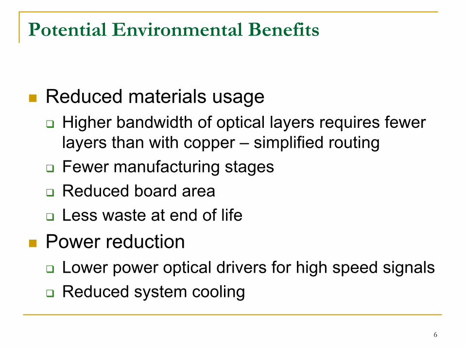
Potential Environmental Benefits
Reduced materials usageHigher bandwidth of optical layers requires fewer layers than with copper – simplified routingFewer manufacturing stagesReduced board areaLess waste at end of life
Power reductionLower power optical drivers for high speed signalsReduced system cooling
7
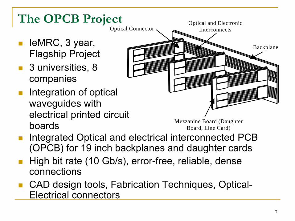
The OPCB Project
Integrated Optical and electrical interconnected PCB (OPCB) for 19 inch backplanes and daughter cardsHigh bit rate (10 Gb/s), error-free, reliable, dense connectionsCAD design tools, Fabrication Techniques, Optical-Electrical connectors
Optical and ElectronicInterconnects
Backplane
Mezzanine Board (DaughterBoard, Line Card)
Optical Connector
IeMRC, 3 year, Flagship Project3 universities, 8companies Integration of optical waveguides with electrical printed circuit boards
8
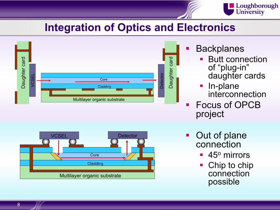
Integration of Optics and Electronics
BackplanesButt connection of “plug-in”daughter cardsIn-plane interconnection
Focus of OPCB project
Out of plane connection
45o mirrorsChip to chip connection possible
Multilayer organic substrate
Core
CladdingVC
SEL
Dau
ghte
r car
d
Det
ecto
r
Dau
ghte
r car
d
DetectorVCSEL
Core
Cladding
Multilayer organic substrate
9
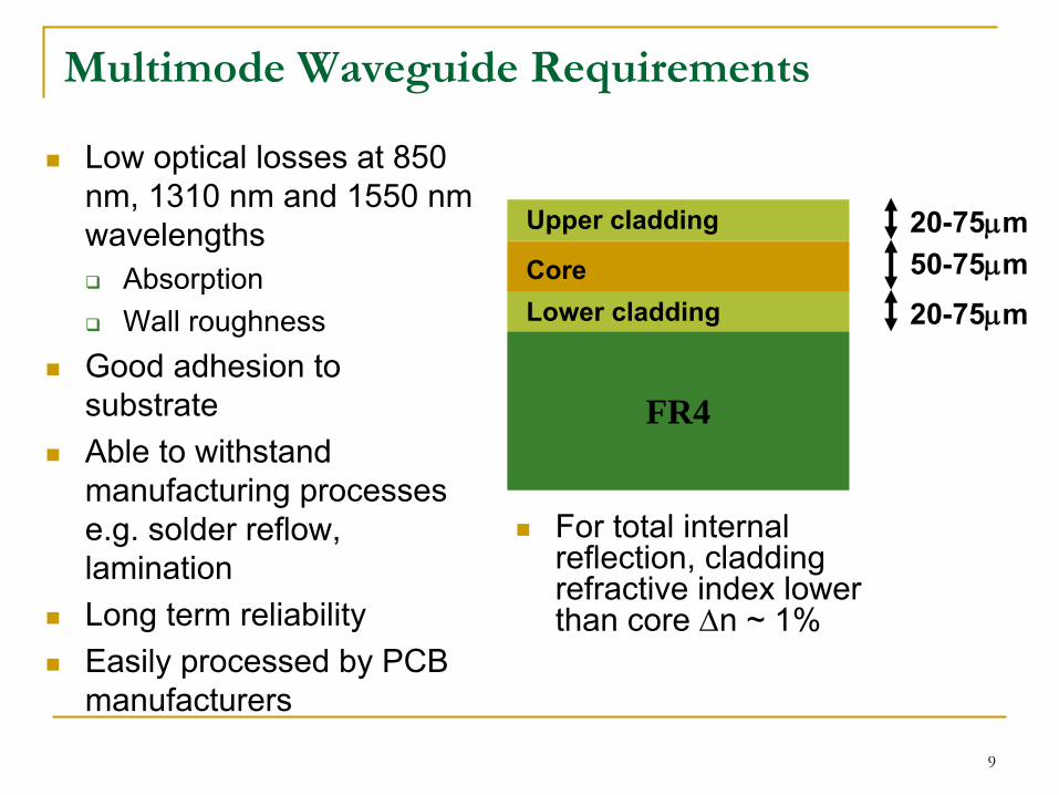
Multimode Waveguide Requirements
For total internal reflection, cladding refractive index lower than core Δn ~ 1%
FR4
Lower cladding
Upper cladding
Core 50-75μm20-75μm
20-75μm
Low optical losses at 850 nm, 1310 nm and 1550 nm wavelengths
Absorption Wall roughness
Good adhesion to substrateAble to withstand manufacturing processes e.g. solder reflow, laminationLong term reliability Easily processed by PCB manufacturers
10
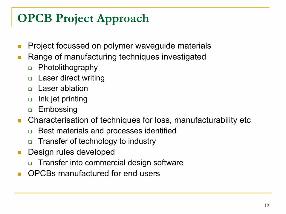
OPCB Project Approach
Project focussed on polymer waveguide materialsRange of manufacturing techniques investigated
Photolithography Laser direct writing Laser ablationInk jet printingEmbossing
Characterisation of techniques for loss, manufacturability etcBest materials and processes identifiedTransfer of technology to industry
Design rules developed Transfer into commercial design software
OPCBs manufactured for end users
11
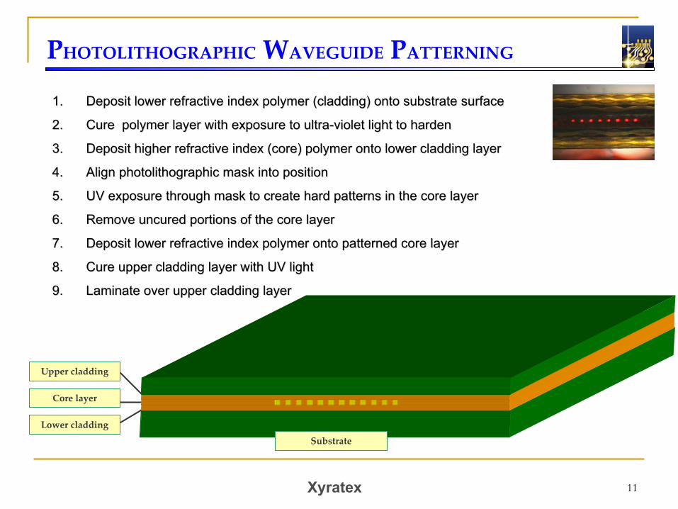
PHOTOLITHOGRAPHIC
WAVEGUIDE
PATTERNING
Substrate
Core layer
Upper cladding
Lower cladding
1.1.
Deposit lower refractive index polymer (cladding) onto substrateDeposit lower refractive index polymer (cladding) onto substrate
surfacesurface
2.2.
Cure polymer layer with exposure to ultraCure polymer layer with exposure to ultra--violet light to hardenviolet light to harden
3.3.
Deposit higher refractive index (core) polymer onto lower claddiDeposit higher refractive index (core) polymer onto lower cladding layerng layer
4.4.
Align photolithographic mask into positionAlign photolithographic mask into position
5.5.
UV exposure through mask to create hard patterns in the core layUV exposure through mask to create hard patterns in the core layerer
6.6.
Remove uncured portions of the core layerRemove uncured portions of the core layer
7.7.
Deposit lower refractive index polymer onto patterned core layerDeposit lower refractive index polymer onto patterned core layer
8.8.
Cure upper cladding layer with UV lightCure upper cladding layer with UV light
9.9.
Laminate over upper cladding layerLaminate over upper cladding layer
Waveguides
11
FS Overview
| Richard Pitwon
Xyratex

12
•
Direct Laser-writing of waveguides•
Increase writing speeds and manufacturability
•
Writing over large areas (400-500mm long)•
Photo-polymer Formulation•
Optimise for faster writing; alternative polymer systems; possible dry formulation
•
Options:•
Custom multifunctional acrylate
polymer
•
Exxelis
formulations•
Polymer Properties•
Tunable
refractive index & viscosity
•
High glass transition temperature
HWU Contribution to OPCB ProjectAndy Walker, Aongus
McCarthy, Himanshu
Suyal

13
Direct Laser-writing Set-up
•
UV-illuminated square aperture (50 μm)
imaged, 1-to-1, onto polymer- coated substrate, carried on computer-controlled x-y stage.
•
Three beams available –
to write:
(a) vertically-walled features, or (b) plus/minus 45-deg structures.

14
Laser written polymer structures
SEM images of polymer structures written using imaged 50 µm square aperture (chrome on glass)

15
Out-of-plane coupling, using 45-deg mirror (silver)
Microscope image looking down on mirror coupling
light towards camera
OPTICAL INPUT
Waveguide terminated with 45o
mirror

16
Laser Ablation for Waveguide Fabrication
Ablation to leave waveguidesExcimer laser – LoughboroughNd:YAG – Stevenage Circuits
FR4 PCBCladding
Core
FR4 PCBDeposit cladding and
core layers on substrateLaser ablate polymer
FR4 PCBDeposit cladding layer
UV LASER
SIDE VIEW
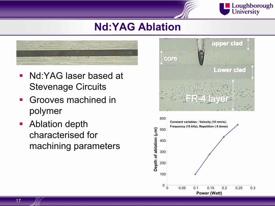
17
Nd:YAG
Ablation
FRFRFR---4 layer4 layer4 layer
Lower cladLower cladLower clad
corecorecore
upper cladupper cladupper clad
0 0.05 0.1 0.15 0.2 0.25 0.30
100
200
300
400
500
600
Power (Watt)
Dep
th o
f abl
atio
n (μ
m)
Constant variables : Velocity (10 mm/s);Frequency (10 kHz); Repetition ( 6 times)
Nd:YAG laser based at Stevenage CircuitsGrooves machined in polymerAblation depth characterised for machining parameters
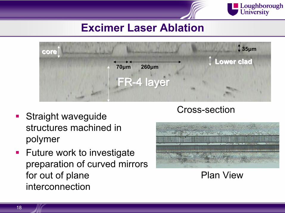
18
Excimer
Laser Ablation
Straight waveguide structures machined in polymerFuture work to investigate preparation of curved mirrors for out of plane interconnection
corecorecoreLower cladLower cladLower clad
FRFRFR---4 layer4 layer4 layer260μm70μm
35μm
Plan View
Cross-section

19
Ink Jet Deposition of Polymer WaveguidesLocalised deposition of cladding and / or core materials
More materials efficientActive response to local features
Printing UV cure materialDeposit liquid, then cure
INK
Print head
Ink deposits
Substrate positioning- CAD data
High Speed Camera Images
20
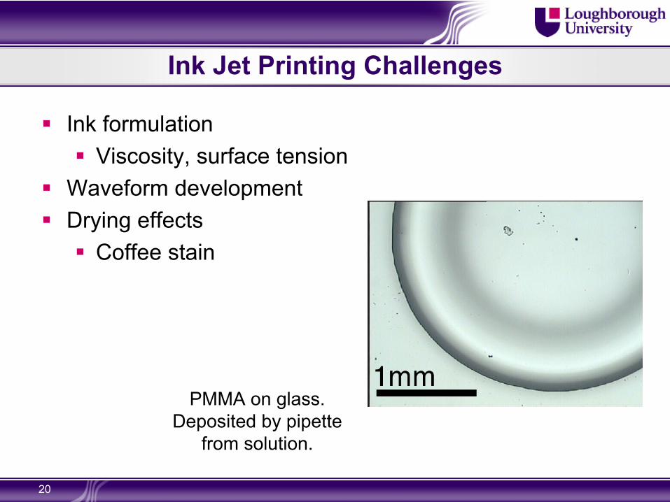
Ink Jet Printing Challenges
Ink formulationViscosity, surface tension
Waveform developmentDrying effects
Coffee stain
PMMA on glass. Deposited by pipette
from solution.
21
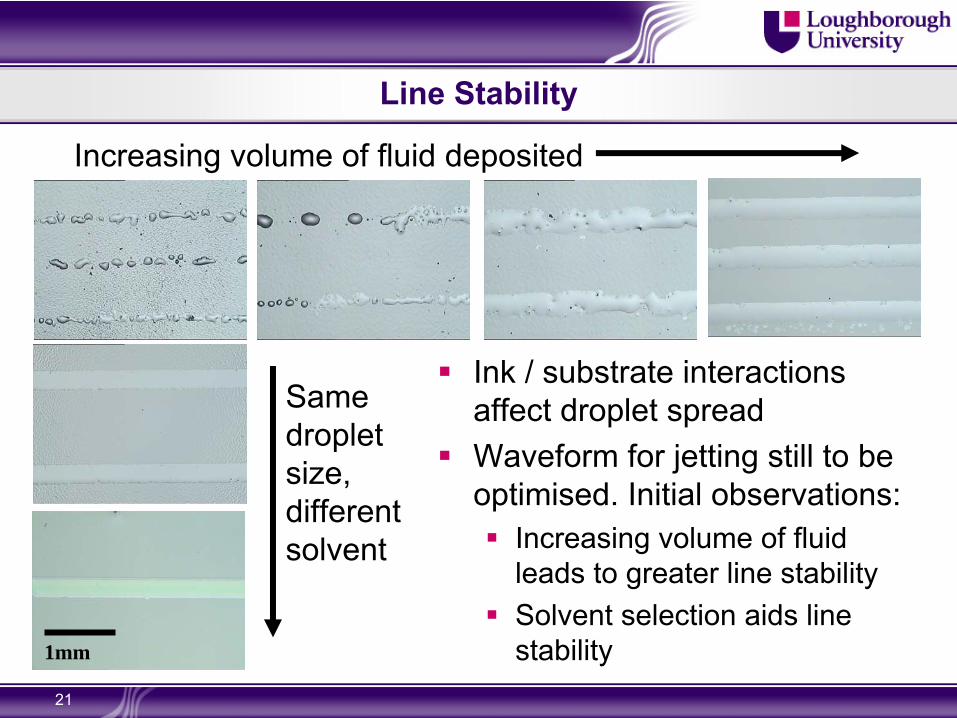
Line Stability
Ink / substrate interactions affect droplet spreadWaveform for jetting still to be optimised. Initial observations:
Increasing volume of fluid leads to greater line stabilitySolvent selection aids line stability
Increasing volume of fluid deposited
1mm
Same dropletsize, different solvent
22
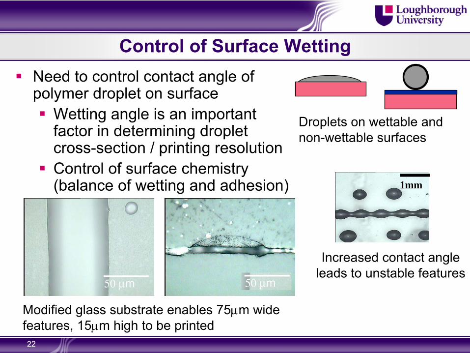
Control of Surface WettingNeed to control contact angle of polymer droplet on surface
Wetting angle is an important factor in determining droplet cross-section / printing resolutionControl of surface chemistry (balance of wetting and adhesion)
Increased contact angle leads to unstable features
Droplets on wettable
and non-wettable
surfaces
1mm
Modified glass substrate enables 75μm wide features, 15μm high to be printed

23Copyright © 2007 UCLCopyright ©
2007 UCL
Waveguide Characterisation
at UCL David R. Selviah, Kai Wang, Ioannis
Papakonstantinou, F. Anibal
Fernández
•
Waveguide Key Component Layout Design •
Optical Printed Circuit Board
(OPCB) Design
•
Waveguide Measurement –
Loss, Bit Error Rate, Eye Diagram, Misalignment Tolerance, Wall Roughness
•
Reliability Assessment–
Humidity, temperature cycling, vibration, aging characteristics
•
Modelling and Experimental comparison→ Design rules to be fed into software tools
24
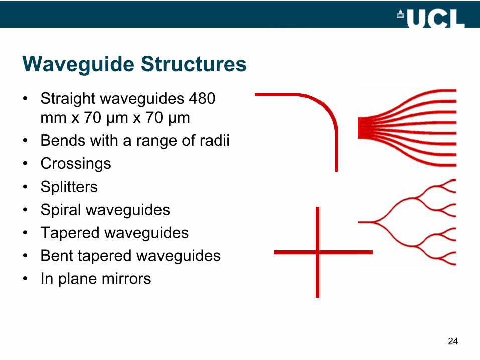
Waveguide Structures•
Straight waveguides 480 mm x 70 µm x 70 µm
•
Bends with a range of radii•
Crossings
•
Splitters•
Spiral waveguides
•
Tapered waveguides•
Bent tapered waveguides
•
In plane mirrors
25
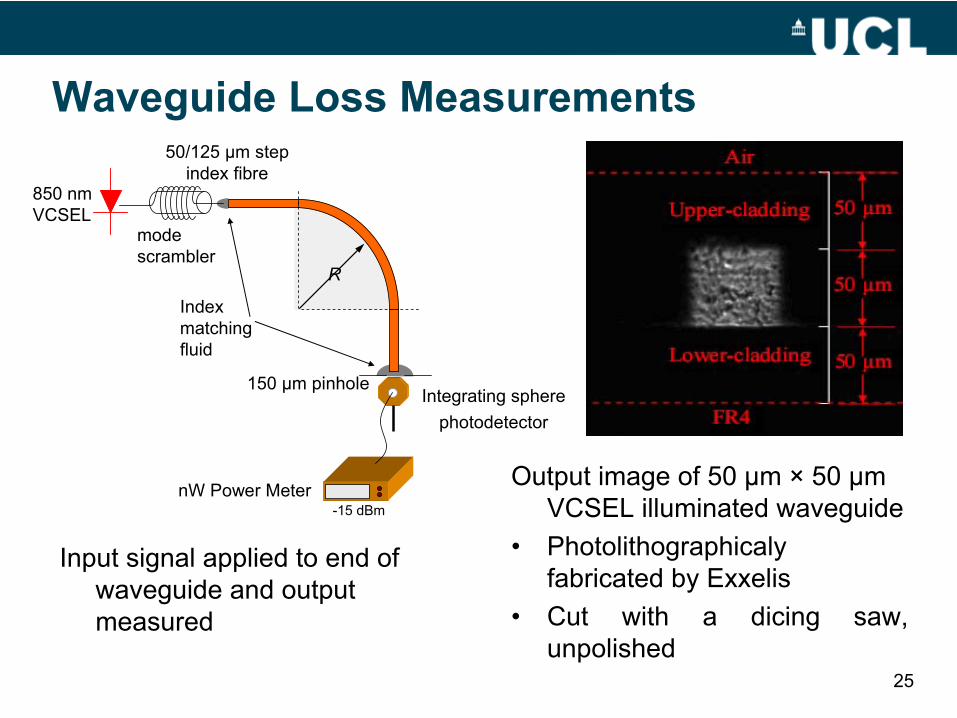
Waveguide Loss Measurements
Output image of 50 μm ×
50 μm VCSEL illuminated waveguide
•
Photolithographicaly fabricated by Exxelis
•
Cut with a dicing saw,
unpolished
850 nm VCSEL
Integrating sphere photodetector
150 μm pinhole
nW Power Meter
50/125 μm step index fibre
mode scrambler
-15 dBm
R
Index matching fluid
Input signal applied to end of waveguide and output measured

26
Transition Loss
w
lin
lout
Rs
Rs +ΔR
Rf = Rs + NΔR
A
B
I
Output
Input
O
Schematic diagram of one set of curved waveguides.
Light through a bent waveguide of R
= 5.5 mm –
34.5 mm
• Radius R, varied between 5 mm < R < 35 mm, ΔR
= 1 mm•
Light lost due to scattering, transition loss, bend loss, and reflection
and back-scattering • Illuminated by a MM fiber
with a red-laser.
27
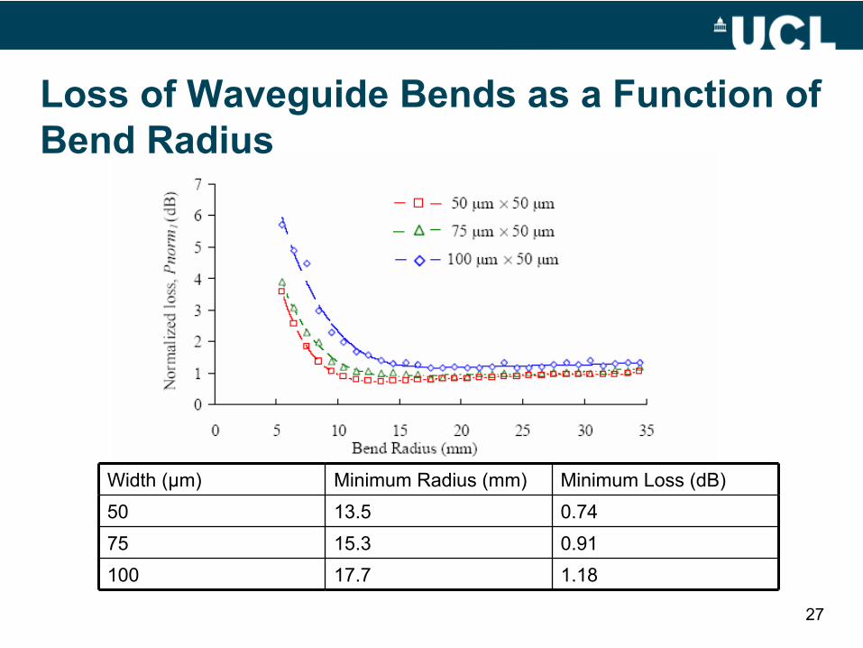
Loss of Waveguide Bends as a Function of Bend Radius
Width (μm) Minimum Radius (mm) Minimum Loss (dB)50 13.5 0.7475 15.3 0.91100 17.7 1.18
28
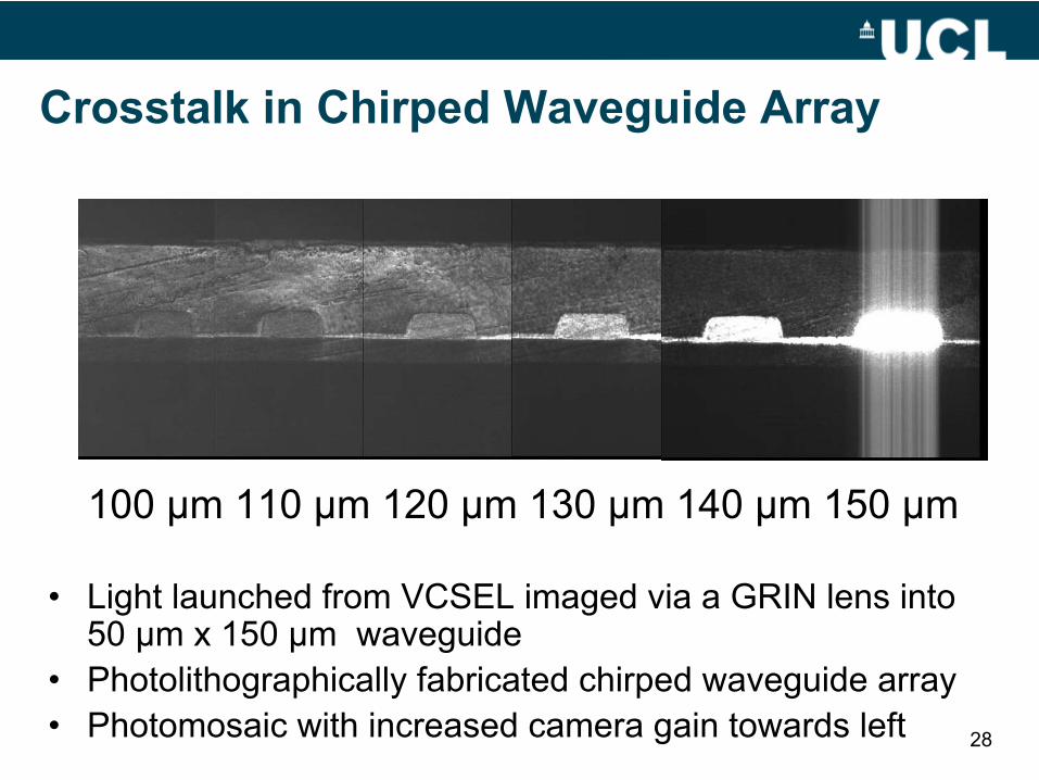
Crosstalk in Chirped Waveguide Array
•
Light launched from VCSEL imaged via a GRIN lens into 50 µm x 150 µm waveguide
•
Photolithographically
fabricated chirped waveguide array•
Photomosaic
with increased camera gain towards left
100 µm 110 µm 120 µm 130 µm 140 µm 150 µm

29
Conclusion
OPCB project investigating the fabrication of polymer waveguides for electrical-optical PCB backplanesSeveral materials and fabrication techniques under investigationWaveguides characterised for loss, wall roughness and long term reliability

30
Acknowledgements
EPSRC for funding through the Innovative Electronics Manufacturing Research Centre (IeMRC)Industrial collaborators:
XyratexExxelisBAE SystemsStevenage Circuits LtdCadenceDow CorningRenishawNPL