improved laser-induced forward transfer of organic...
TRANSCRIPT

Appl Phys A (2011) 105:713–722DOI 10.1007/s00339-011-6583-x
Improved laser-induced forward transfer of organicsemiconductor thin films by reducing the environmental pressureand controlling the substrate–substrate gap width
James Shaw-Stewart · Bryan Chu · Thomas Lippert ·Ylenia Maniglio · Matthias Nagel · Frank Nüesch ·Alexander Wokaun
Received: 3 June 2011 / Accepted: 24 August 2011 / Published online: 23 September 2011© Springer-Verlag 2011
Abstract Laser-induced forward transfer (LIFT) has beeninvestigated for bilayer transfer material systems: silver/organic film (Alq3 or PFO). The LIFT process uses anintermediate dynamic release layer of a triazene polymer.This study focuses on the effect of introducing a controlleddonor–receiver substrate gap distance and the effect of do-ing the transfer at reduced air pressures, whilst varying thefluence up to ∼200 mJ/cm2. The gap between ‘in-contact’substrates has been measured to be a minimum of 2–3 µm.A linear variation in the gap width from ‘in contact’ to40 µm has been achieved by adding a spacer at one sideof the substrate–substrate sandwich. At atmospheric pres-sure, very little transfer is achieved for Alq3, although PFOshows some signs of successful doughnut transfer (with alarge hole in the middle) in a narrow fluence range, at gapsgreater than 20 µm. For the transfer of Ag/PFO bilayers at at-mospheric pressure, the addition of a PFO layer onto the re-ceiver substrate improved the transfer enormously at smallergaps and higher fluences. However, the best transfer resultswere obtained at reduced pressures where a 100% transfersuccess rate is obtained within a certain fluence window.The quality of the pixel morphology at less than 100 mbar ismuch higher than at atmospheric pressure, particularly when
J. Shaw-Stewart (�) · B. Chu · Y. Maniglio · M. Nagel ·F. NüeschLaboratory for Functional Polymers, Empa Swiss FederalLaboratories for Materials Science and Technology,Überlandstrasse 129, 8600 Dübendorf, Switzerlande-mail: [email protected]
J. Shaw-Stewart · T. Lippert · A. WokaunMaterials Group, General Energies Department, Paul ScherrerInstitut, 5232 Villigen-PSI, Switzerland
T. Lipperte-mail: [email protected]
the gap width is less than 20 µm. These results show thepromise of LIFT for industrial deposition processes where agap between the substrates will improve the throughput.
1 Introduction
Early laser-based material transfer was carried out as longago as 1970 on ink [1] and was followed by the trans-fer of metals using a similar technique in the 1980s [2].These experiments marked the precursor to laser-inducedforward transfer (LIFT), which has been subsequently im-proved with the use of an absorbing intermediate layer. LIFTis now used for the transfer of complex functional materi-als [3, 4]. Recently, research into LIFT has intensified andvarious different materials have been transferred includingmicroorganisms [5], biological cells [6], biomolecule solu-tions [7], quantum dots [8], organic light-emitting diodes(OLEDs) [9], organic thin-film transistors [10], ceramics[11], 3-D interconnects [12], polystyrene microbeads [13],polymeric sensors [14], and liposomes [15]. Many of thesebreakthroughs used an absorbing intermediate layer, termedthe dynamic release layer (DRL). The DRL is often an in-organic thermal absorber, such as titanium [16], or a poly-mer that breaks down in a photon-induced chemical reac-tion, such as the class of triazene polymers [17].
LIFT for the fabrication of polymeric OLEDs (PLEDs)has already been investigated [9, 17]. The observations fromthose studies included good functionality of the transferreddevices, different transfer qualities onto different receiversubstrates, and also some minor cracking within the pixel.Overall, the process looked a success, but one feature ap-peared undesirable: the pressing of the substrates together‘in contact’. There were two distinct disadvantages to thison the laboratory scale. Firstly, transfer ‘in contact’ often

714 J. Shaw-Stewart et al.
caused the pixel to adhere to both the donor substrate andthe receiver substrate after the laser ablation. This meant thatseparating the substrates was crucial to successful deposi-tion. The second problem was that ‘in contact’ is not actu-ally in contact. A small gap of some width must be present,and the problem of a single dust particle ruining the trans-fer by increasing this gap width was observed. In addition,shadowgraphy experiments have shown the generation of aconsiderable shock wave at atmospheric pressure [18–20].Reduced pressure and transfer across large gap widths (0.5and 1 mm) have both already been investigated using shad-owgraphy [19]. That investigation showed the effect of thereflected shock wave in destroying the flyers at atmosphericpressure. It also showed that the transfer was unsuccessful atreduced pressures, because the flyers either folded too muchat low fluences or were destroyed on impact at higher flu-ences.
In this study the effect of different gap widths of up to40 µm has been investigated at atmospheric pressure and atreduced pressures, for the LIFT setup shown in Fig. 1. Wehave successfully transferred bilayer thin-film pixels acrossa gap. The main previous investigation used much largergaps than we have used here (500 vs. 40 µm) [19]. The largergap, along with the lack of coating on the glass receiver sub-strate, may explain why the transfer was not successful pre-viously, but has been successfully achieved across a gap inthis study. Previous observations of the destructive nature ofthe shock wave at atmospheric pressure [19] have been re-affirmed, and the benefit of reducing the air resistance, andthe shock wave, by reducing the pressure further supportsthis observation. The recent observation that the transfer de-pended on the receiver substrate [17] has also been followedup by adding a layer of the organic material used in the trans-fer onto the receiver substrate to improve the pixel–receiversubstrate adhesion at atmospheric pressures.
The DRL material in this study is a triazene polymer (TP)with the chemical structure shown in Fig. 2a. The metal usedis silver, a standard electrode material for OLEDs, includingthe very first OLED devices in 1987 [21]. The first OLEDswere made with an electroluminescent layer of Alq3 (alu-minium tri-8-hydroxyquinoline, shown in Fig. 2b). Alq3 isa small molecule and has already been a material of inter-est for OLED transfer [16]. Our previous investigations intoPLEDs have focussed on MEH-PPV (poly[2-methoxy, 5-(2-ethylhexyloxy)-1,4-phenylene vinylene]) [9, 17, 19]. How-ever, in this study we have changed our conjugated polymerof interest to PFO (poly[9,9-dioctylfluorene-2,7-diyl] shownin Fig. 2c). PFO is used variously as a blue emitter, a hostfor phosphorescent dyes, and a starting point for more com-plex homo- and copolymers [22]. We have also observedPFO to have better spin-coated film formation propertiesthan MEH-PPV.
Fig. 1 A schematic outlining the LIFT process, as detailed in the pa-per: Step 1 shows the donor and receiver substrates, pressed togetherwith a spacer between them, in the gas chamber with a laser pulse com-ing towards them; Step 2 shows the sample during the transfer process;Step 3 shows the removed receiver substrate after the transfer
Fig. 2 The organic materials’ chemical structures used in these exper-iments. (a) Is the triazene polymer used as the DRL; (b) is Alq3, thesmall-molecule OLED material; (c) is PFO, the blue-emitting poly-meric OLED material; (d) is PEDOT; and (e) is PSS. (a)–(c) Wereused on the donor substrate, and a blend of (d) and (e) was used on thereceiver substrate
Improved laser-induced forward transfer of organic semiconductor thin films by reducing the environmental 715
2 Experimental
2.1 Sample preparation
High-quality Suprasil fused silica substrates (25 × 25 ×1 mm3) have been used for the donor substrates, andplain glass microscope slides (∼ 25 × 25 × 1 mm3) havebeen used for the receiver substrates. Both substrates werecleaned in a series of ultrasonic baths: acetone, ethanol,alkali surfactant (Hellmanex™, Hellma AG), and water.The donor substrates were additionally cleaned using aUV–ozone cleaner before final bathing in microfilteredwater. The receiver substrates were next coated with PE-DOT:PSS (poly[3,4-ethylenedioxythiophene] blended withpoly[styrenesulfonate]). The PEDOT:PSS (Clevios™PAl4083) was spin coated at 6000 rpm to give a film 30 nmthick. The chemical structures for PEDOT and PSS areshown in Fig. 2d and e.
The triazene polymer (TP) used here (Fig. 2a) was syn-thesized according to the procedure outlined before forTP-6a [23, 24]. The triazene polymer was dissolved in cy-clohexanone:chlorobenzene solution at varying concentra-tions of up to 5 wt%. The donor substrates were spin coatedwith triazene polymer and the thicknesses measured usingan Ambios XP-1 profilometer. The Ag layer was then evap-orated onto the TP. For the initial atmospheric pressure mea-surements, thick Ag layers (200 nm) were used to try to in-crease the mechanical stability of the flyer. For the donorsubstrates transferred onto the PFO/PEDOT:PSS receiversubstrates, a 150 nm Ag layer was used. For the samplesused in the reduced pressure experiments, an 80 nm Aglayer was used. The thicknesses were measured in-situ us-ing a quartz crystal microbalance. On top of the Ag, ei-ther 80 nm Alq3 was evaporated or 80 nm PFO was spincoated from a toluene:p-xylene (1:1 wt) solution (15 mg/ml,1500 rpm). The Alq3 was bought from Sigma Aldrich (sub-limed grade) and the PFO from American Dye Source. Thechemical structures for Alq3 and PFO are shown in Fig. 2band c.
2.2 Experimental setup
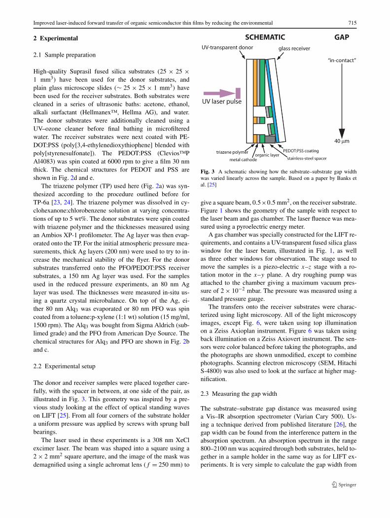
The donor and receiver samples were placed together care-fully, with the spacer in between, at one side of the pair, asillustrated in Fig. 3. This geometry was inspired by a pre-vious study looking at the effect of optical standing waveson LIFT [25]. From all four corners of the substrate holdera uniform pressure was applied by screws with sprung ballbearings.
The laser used in these experiments is a 308 nm XeClexcimer laser. The beam was shaped into a square using a2 × 2 mm2 square aperture, and the image of the mask wasdemagnified using a single achromat lens (f = 250 mm) to
Fig. 3 A schematic showing how the substrate–substrate gap widthwas varied linearly across the sample. Based on a paper by Banks etal. [25]
give a square beam, 0.5×0.5 mm2, on the receiver substrate.Figure 1 shows the geometry of the sample with respect tothe laser beam and gas chamber. The laser fluence was mea-sured using a pyroelectric energy meter.
A gas chamber was specially constructed for the LIFT re-quirements, and contains a UV-transparent fused silica glasswindow for the laser beam, illustrated in Fig. 1, as wellas three other windows for observation. The stage used tomove the samples is a piezo-electric x–z stage with a ro-tation motor in the x–y plane. A dry roughing pump wasattached to the chamber giving a maximum vacuum pres-sure of 2 × 10⁻² mbar. The pressure was measured using astandard pressure gauge.
The transfers onto the receiver substrates were charac-terized using light microscopy. All of the light microscopyimages, except Fig. 6, were taken using top illuminationon a Zeiss Axioplan instrument. Figure 6 was taken usingback illumination on a Zeiss Axiovert instrument. The sen-sors were color balanced before taking the photographs, andthe photographs are shown unmodified, except to combinephotographs. Scanning electron microscopy (SEM, HitachiS-4800) was also used to look at the surface at higher mag-nification.
2.3 Measuring the gap width
The substrate–substrate gap distance was measured usinga Vis–IR absorption spectrometer (Varian Cary 500). Us-ing a technique derived from published literature [26], thegap width can be found from the interference pattern in theabsorption spectrum. An absorption spectrum in the range800–2100 nm was acquired through both substrates, held to-gether in a sample holder in the same way as for LIFT ex-periments. It is very simple to calculate the gap width from

716 J. Shaw-Stewart et al.
Fig. 4 Light microscopy images of the donor substrates consistingof fused silica/190 nm TP/200 nm Ag/ (a) 80 nm Alq3 or (b) 80 nmPFO. The flyers are in the middle of the ablation spot after back-side
ablation with a fluence of 70 mJ/cm2, with a linearly varying gap tothe receiver substrate (glass/30 nm PEDOT:PSS)
the interference in these spectra, assuming the refractive in-dex of air to be 1. Using this method, the gap width for thesamples ‘in contact’ was calculated to be 2–3 µm, but waseasily increased to >10 µm with small amounts of dust con-tamination.
To try and control the gap width, stainless steel with well-defined thickness (Brütsch Rüegger) was cut into the rightshape for the sample holder. A variation in gap width acrossthe sample was achieved by adding the spacer at one side,as shown in Fig. 3. However, because of the limitations ofthe size of the light beam for the absorption spectrometer,measurements of the gap width along the gradient could notbe made. The gap width can only be measured for a con-stant gap width. To measure the variation in gap width inFig. 3, the gap was measured with the spacer in and thenan assumption of a linear gap gradient is made between thespacer and the ‘in-contact’ edge. At atmospheric pressure,the spacer used was 40 µm, and transfers were carried outacross the whole sample, i.e. from a gap width of 40 µmto ‘in contact’. Because of the travel-distance limitations ofthe piezoelectric stage in the gas chamber (∼7 mm maxi-mum), a 100 µm spacer was used, and the transfers started3/5th of the way across the sample from the spacer, allow-ing for approximately the same range of gap widths as theatmospheric pressure experiments: about 40 to 5 µm.
3 Results
3.1 Effect of adding a gap
The initial transfers at atmospheric pressure were done us-ing donor substrates with a thick (200 nm) Ag layer. Themain advantage of using a thicker layer was to prevent theflyer from fragmenting, which it does fairly easily at atmo-spheric pressure. The triazene DRL thickness was constantat 190 ± 10 nm for these experiments. The setup yielded a
matrix of attempted transfers with decreasing gap, from leftto right, and increasing fluence, down the sample.
The transfer material will be referred to as a flyer whenit is still on the donor substrate, and a pixel when it is de-posited on the receiver substrate. It must be emphasized thatfor both Alq3- and PFO-coated donor substrates the thresh-old fluence for ejection without a receiver substrate is around50 mJ/cm2. Attempted transfers of Alq3 onto a receiver sub-strate resulted in almost no pixel deposition. The donor sub-strate for Alq3 is shown in Fig. 4a, for ablation at a fluenceof 70 mJ/cm2, with the gap increasing from right to left. Asthe gap increases, the size of the flyer starts to shrink, and ahole also appears in the middle. The hole only really startsat a minimum gap distance of ∼20 µm, at about the sametime as the flyer starts to get noticeably smaller. It appearsthat the flyer is smaller at larger gap distances because theedges fold up, particularly in the corners.
Except for the organic layer material, Fig. 4b (PFO)shows the same donor substrate as Fig. 4a (Alq3). PFOshows a similar trend to that observed for Alq3, but thereis less clearly defined flyer contact with the donor substrate.For the flyers between 5 and 20 µm gap the trend looks verysimilar, but above 20 µm the flyers appear more distorted.Overall, the area in contact with the donor substrate is lessclear for PFO than for Alq3, and the edges are not folded inthe same uniform fashion as for Alq3. For the fourth abla-tion crater from the left, at a gap width of 25–30 µm, the flyeris not present, indicating that a pixel has been deposited onthe receiver substrate, which has indeed been observed (seeFig. 5, pixel circled in red).
Figure 5 shows the receiver substrate with pixels trans-ferred from the 200 nm Ag/80 nm PFO donor substratefrom Fig. 4b. The corresponding Ag/Alq3 pixels were nottransferred as successfully. The transferred Ag/PFO pix-els clearly have a hole in the middle of them, and have ashape akin to a holed doughnut. At fluences greater than86 mJ/cm2, no pixel transfer was observed. The optimal flu-ence is around 80 mJ/cm2.

Improved laser-induced forward transfer of organic semiconductor thin films by reducing the environmental 717
Fig. 5 Light microscopy images of the receiver substrate for the190 nm TP/200 nm Ag/80 nm PFO donor substrate where transfer wasachieved, but of non-functional pixels. A distinctive doughnut shape tothe transferred pixels can be observed. The edges of the pixel, and thehole in the middle, are in contact with the substrate
3.2 Effect of modifying the receiver substrate
It was observed in a recent study that the receiver substratecan play a significant role in the transfer [17]. This obser-vation suggested that adhesion between the flyer and thereceiver substrate was a large part of the influence of thereceiver substrate. Following on from these observations, inthis study the receiver substrate has been modified by addingthe organic material that is being transferred from the donorsubstrate (PFO in Fig. 6) onto the receiver substrate. ForAlq3, this proved to make very little difference, but the ob-servations for PFO were interesting.
Figure 6 shows two different receiver substrates forthe same donor substrate. Figure 6a shows an ordinaryglass/PEDOT:PSS receiver substrate with the red rectanglecorresponding approximately to the same fluence and gapwindow as Fig. 5. Figure 6b shows the same receiver sub-strate, but coated with an additional 80 nm PFO layer. Theaddition of PFO onto the receiver substrate clearly improvesthe likelihood of the transfer at smaller gaps and higher flu-ences (green rectangle). In addition, the pixels have a bettershape at smaller gaps, <20 µm, without the hole in the mid-dle, and a sharper square frame.
Whilst the transfer at 20–40 µm in Fig. 6a, shown inthe red rectangle, is not quite as good as that observed inFig. 5, the pattern is the same, with most of the success-ful transfers at gaps of 20–40 µm. These results for 150and 200 nm Ag can also be compared with a comparablereceiver substrate for 80 nm Ag in Fig. 7a, with the rele-vant fluence and gap range again in a red rectangle. Theseimages show a distinct trend in terms of the influence ofthe metal layer thickness on the success rate of transferringthese PFO pixels. In Fig. 5, the Ag layer of the donor sub-strate was 200 nm thick, in Fig. 6a it was 150 nm thick, andin Fig. 7a it was 80 nm thick. This shows that the thicker theAg layer is, the better the chance of successful pixel depo-sition at gaps of 20–40 µm. However, it cannot be said that
Fig. 6 Microscopy images of receiver substrates of PFO transfers,back illuminated. The donor substrate for both was 190 nm TP/150 nmAg/80 nm PFO. (a) Is an ordinary receiver substrate, glass coated with30 nm PEDOT:PSS, and (b) is the same as (a), but with 80 nm PFOspin coated onto the PEDOT:PSS. Fluences are in mJ/cm2
the transfer is altogether successful, even in Fig. 5, giventhe doughnut shape of the pixels, which would almost cer-tainly make non-functional devices. The pixels at low gapsand high fluences in Fig. 6b may make functional devices,but the use of PFO on both the receiver and donor sub-strates is not the goal in terms of PLED device architec-ture.
3.3 Effect of pressure reduction
Despite some successes with the PFO transfer across a gapin ambient conditions, it is clear that most of the depositedpixels would not be functional. For this reason, the envi-ronmental pressure in the gas chamber was reduced from1 bar (atmospheric pressure) to 3 × 10⁻² mbar. The samplesfor these experiments were the same as those used before,except that only 80 nm Ag was used. Thinner silver filmswere used to highlight the improvement in transfer qualitybecause thinner metal films show noticeably poorer transferat atmospheric pressure: see the red box in Fig. 7a comparedto Fig. 5 and the red box in Fig. 6a.

718 J. Shaw-Stewart et al.
Fig. 7 Light microscopy and SEM images of the PEDOT:PSS-coatedglass receiver substrates for 190 nm TP/80 nm Ag/80 nm PFO donorsubstrates with different environmental pressures. (a) Is atmosphericpressure (1000 mbar), and each subsequent picture from (b) to (f) is
one order of magnitude lower. The fluence goes down from top to bot-tom, and the gap increases, from 5 to 40 µm, from right to left. Fig-ures (g) to (i) are SEM images of the pixel at ∼5 µm gap distance and78 mJ/cm2, for: (g) 100 mbar, (h) 1 mbar, and (i) 0.03 mbar
3.3.1 Pressure improvement
Figure 7 shows the large improvement of pixel transfer atreduced pressures. At 100 mbar (Fig. 7b) the transfer is al-ready greatly improved and, below 10 mbar (Fig. 7c–f), thetransfer is even better, but does not obviously improve withfurther pressure reduction. There is a degree of variationfrom sample to sample, but this is negligible, and probablydependent on the long-term variation in laser energy (∼5%).In addition, the standard deviation of the fluence varied by±5% from pulse-to-pulse instability. Nevertheless, the pres-sure trend is fairly clear, and the transfer consistency below10 mbar is obvious: rows 3–6 (from top) are all completely
transferred for all of Fig. 7c–f, 10–0.3 mbar. The close-up SEM images, Fig. 7g–i, show three main observations.Firstly, there is folding just inside the edges. The folding ismore pronounced at lower fluences, e.g. the single lines par-allel to the pixel edges for pixels transferred at 55 mJ/cm2 inFig. 7c–f. They are particularly prominent within the pixelat low fluences and gap distances (an example is shown witha green ellipse in Fig. 7h). Secondly, irregular ripping of themetal along the edges can be clearly seen. Figure 8 suggeststhat the metal ripping is partly fluence dependent. An addi-tional rip/fold is shown in a red ellipse in Fig. 7i to high-light a characteristic feature that appears after a subsequenttransfer close enough to damage the pixel which has already

Improved laser-induced forward transfer of organic semiconductor thin films by reducing the environmental 719
Fig. 8 SEM images ofindividual pixels transferred attwo different fluences and threedifferent gap distances at apressure of 1 mbar (see Fig. 7d).(a) to (c) are at 65 mJ/cm2, and(d) and (e) are at 90 mJ/cm2
been deposited, i.e. it is not a consequence of the originaltransfer. In Fig. 7i the chronology of the transfers goes fromtop to bottom; hence, the transfer in line 5 of Fig. 7d, at90 mJ/cm2, would affect the line above where the pixel inFig. 7i came from. The precise mechanism for this post-depositional effect is not clear, but is possibly the acousticshock wave from the TP decomposition products. Lastly, astriped pattern can be observed parallel to the edges, partic-ularly the right- and left-hand edges. This pattern has beenhighlighted in Fig. 7g with blue lines. Supplementary to thislast observation are circles which appear to be embedded inthe same way, as a topographical variation, indicated withblue arrows in Fig. 7g.
Figure 8 shows some SEM images of pixels transferredat 1 mbar. The pixels in the first row were transferred at alaser fluence of 65 mJ/cm2 and those in the second row weretransferred at a laser fluence of 90 mJ/cm2. The gap dis-tances for the pixels are shown below the images. As wellas the folding within the pixel in Fig. 8c (green ellipses), thefolding of the edges is far more pronounced in pixels trans-ferred over a larger gap (Fig. 8a and b). The overall effectof the folding is to shrink the pixel, similar to the observa-tion for the Alq3 flyers in ambient pressure in Fig. 4a. Thepixels transferred at higher fluence, 90 mJ/cm2, do not showsuch pronounced folding. However, some curling up of thepixel edges is clear in Fig. 8d. The folding shown in a redellipse is post-depositional damage caused by subsequenttransfers, as explained in the previous paragraph for the pixelin Fig. 7i. The folding/curling-up observations from Fig. 8
match the shape of the flyers observed in shadowgraphic in-vestigations at reduced pressure [19]. The shadowgrams inthat paper showed that the flyer edges curled towards thedonor substrate, the same direction as the folding in theseSEM observations of pixels transferred at reduced pressure.
An additional observation from the SEM images is theregularity of the topological patterns, other than the folding.These patterns are hard to interpret and it is not clear whatthey are exactly. The stripes along the edges highlighted byblue lines in Fig. 7g are clearly present in some of the pixelsin Fig. 8. The circular patterns indicated with blue arrowsin Fig. 7g are also clearly present in some of the pixels inFig. 8, too. The circular patterns appear to be located in thesame places of the pixel, irrespective of the sample and pres-sure. Without additional research it is hard to interpret thesepatterns, but similar oscillatory patterns have been observedin front-side ablation of triazene before [27, 28].
3.3.2 Triazene DRL thickness comparison
In addition to the pressure and substrate–substrate gap de-pendence, the effect of changing the triazene DRL thick-ness was also investigated. The two extremes for successfultransfer of 300 and 100 nm are shown in Fig. 9. The only TPfilm thinner than 100 nm that we investigated, 40 nm, didnot appear to give any successful transfers, and we did notinvestigate thicknesses above 300 nm. Figure 9 shows thebig difference in transfer success for 100 nm and 300 nm

720 J. Shaw-Stewart et al.
Fig. 9 Light microscopy images of the PEDOT:PSS-coated receiversubstrates for TP/80 nm Ag/80 nm PFO donor substrate transfers at arange of fluences and gap distances. The pressure is 1 mbar. (a) Is fora donor substrate TP DRL thickness of 100 nm and (b) is for a donorsubstrate TP DRL thickness of 300 nm
TP at 1 mbar, with varying gap distance, as a function of flu-ence. Successful transfer is obtained above 140 mJ/cm2 for300 nm TP DRL, in Fig. 9b, whereas the flyer has been com-pletely disintegrated by 90 mJ/cm2 for 100 nm TP DRL.From front-side-ablation depth measurements of TP, a sin-gle 308 nm pulse of 60 mJ/cm2 is enough to ablate 100 nmTP. More than 150 mJ/cm2 is required to ablate 300 nm TP[29]. This explains the general trend of successful transfer athigher fluences for a greater TP DRL thickness.
4 Discussion
It has been proposed that the shock wave may play a signifi-cant role in affecting the quality of transfer [17]. In an earlierpaper, reduced pressure environments were also investigatedto try and remove the effect of the shock wave [19]. That in-vestigation used time-resolved shadowgraphy to observe theflyer velocity and morphology, and to observe transfers overgaps of 0.5 and 1 mm. Although air resistance was clearlyreduced, folding at low fluences and high impact at high flu-ences meant that transfer was unsuccessful over these biggap widths. It was actually concluded that transfer was bet-ter at atmospheric pressure with gaps of 0.5 and 1 mm [19].
In this study, Fig. 4 shows some of the best evidence forthe power of the shock wave pushing back the flyer ontothe donor substrate. For the Alq3 donor substrates (Fig. 4a)the flyers at the larger gap distances (>20 µm) show a veryinteresting morphology. The edges of the flyer curl up, butan almost circular area of the flyer shows flat, uniform con-tact with the donor substrate. In the middle, a small holeappears like a hole punched through the flyer, resulting ina doughnut shape. The area of the flyer in contact with thedonor substrate appears pressed down by the shock wave,and the edges which curl up are where the shock wave/air re-sistance force has dissipated enough to be too weak to pushthe flyer back onto the donor substrate. This effect shouldincrease dramatically with gap distance, and indeed Fig. 4a
shows this. Although not shown, a deposit is left on thereceiver substrate, which indicates that the flyer comes incontact, or at least close to contact, with the receiver sub-strate before being pushed back onto the donor substrate.Figure 4b does not show the same uniform contact with thedonor substrate as Fig. 4a, presumably because of the dif-ferent material properties of the organic PFO layer vs theAlq3 layer. The polymeric PFO should have better film co-hesion than the small-molecule Alq3, and may well be moreadhesive as well, particularly to another polymeric mate-rial (PEDOT:PSS). Due to the better PFO adhesion, trans-fer is expected to be better in atmosphere compared withAlq3 films (Fig. 5). It may also explain why the PFO flyersare more folded and dishevelled in Fig. 4b than the Alq3 fly-ers in Fig. 4a, because the adhesive force between the flyerand the PEDOT:PSS receiver is closer to the force exertedby the shock wave pushing the flyer back towards the donorsubstrate for PFO than for Alq3.
The improvement in transfer from the addition of thePFO layer onto the receiver substrate, shown in Fig. 6, backsup the hypothesis that the adhesive force between the PFOand the PEDOT:PSS is only just below that of the force pre-venting transfer. The PFO was added onto the receiver sub-strate with the expectation that it will have a higher adhe-sion to the PFO flyers than PEDOT:PSS. A significant in-crease in transfer success is achieved at smaller gaps withthe PFO on the receiver substrate. Previously, we observedthat the addition of PEDOT:PSS greatly improved transferof MEH-PPV ‘in contact’ at low fluences [17]. This resultfurther increases the evidence for the effect of the receiversubstrate upon the quality of transfer. However, it is impor-tant to note that the improvement may not be entirely dueto adhesion, despite the hypothesis. The mechanical proper-ties of the films may play a big role in dissipating energy ineither the shock waves in the gas or from the impact of theflyer. This could also affect the quality of transfer.
Our understanding of the transfer process has been aidedby the control of the gap width on the µm scale. Ontoplain PEDOT:PSS-coated substrates, the PFO transferredmuch better across gaps >20 µm at atmospheric pressure, asshown in Fig. 5. In contrast, MEH-PPV (not shown, but usedin previous investigations [9, 17]) was observed to transferonto PEDOT:PSS well with a gap <10 µm. This explainswhy some degree of inconsistency was observed with MEH-PPV OLEDs ‘in contact’, as light contamination of dust par-ticles increases the gap from ‘in contact’ to >10 µm. At re-duced pressure good transfer appears more consistent, cov-ering a larger range of fluences and gaps (Figs. 7 and 8).The morphology of the transferred pixel is greatly depen-dent on gap width, with significant folding observed evenabove 20 µm at lower fluences in Fig. 7. The reason that thetransferred pixel shrinks as the gap width increases is prob-ably because of the gaseous products of the triazene decom-position pushing their way around the edges of the pixel, as

Improved laser-induced forward transfer of organic semiconductor thin films by reducing the environmental 721
observed in earlier shadowgraphy studies [19]. The largerthe gap, the more this process is allowed to develop, and themore folded the flyer will be. However, this process is alsofluence dependent, as shown in Fig. 8. Increasing the flu-ence will decrease the amount of folding, but at the cost ofablating more of the transfer material.
The transfer improvement by reducing the pressure issignificant, as shown in Fig. 7. At atmospheric pressure,Fig. 7a, transfer of these thin films was very variable anddifficult. At reduced pressures, the transfer is far more re-liable and creates higher quality pixels, demonstrating thebenefit of removing the air resistance and the shock wave,which are both proportional to pressure. In a previous study,the energy in the shock wave was calculated as a functionof fluence [18]. In that article, the shock wave energy wascalculated to be 30–40% of the input laser energy. The flyerkinetic energy was calculated to be ∼3–4%, one order ofmagnitude lower. As the pressure is reduced, the shock waveenergy is reduced. The shock wave energy is directly propor-tional to the gas density, i.e. pressure. Therefore, a single or-der of magnitude reduction in pressure brings the energy ofthe shock wave to the same order of magnitude as the flyer.As has been observed, reducing the shock wave energy in-creases the flyer energy [19]. This means that at ∼100 mbar,the flyer energy will start to be above the shock wave energy,and transfer can be relied upon. Following this hypothesis,it would be expected that below 10 mbar no improvement inthe transfer quality would be observed because the energyof the shock wave should already be at least one order ofmagnitude less than the flyer kinetic energy. The hypothesisis thus backed up by our observations.
A feature common to quite a lot of the data presented hereis the hole in the middle of the pixels creating the doughnutpixels. This is primarily evident in the atmospheric pressuretransfers with gaps above 20 µm, in Figs. 4 and 5. A mi-nor hole is also seen in lower fluence pixels with large gapwidths at reduced pressures, in Fig. 8. The origin of the holemust be because the center of the pixel will experience themaximum shear stress, but at least two mechanisms must bein play because of dual effects of higher pressure and greatergap width, as well as the less significant effect of lower flu-ence, all contributing to increasing the likelihood and sizeof holes in the center of the pixels. It must be consideredthat larger gaps mean that the flyer is in flight for a longertime, allowing heterogeneities to be accentuated. Higher airpressures also slow down the pixel, but additionally haveair resistance and an acoustic shock wave affecting the flyermorphology.
A trend in the influence of the metal layer thickness isshown by Figs. 5, 6a, and 7a. The thicker the Ag metallayer, the better the likelihood of transfer at gaps >20 µmand at atmospheric pressure. Figure 5 uses an Ag layer of200 nm, Fig. 6a an Ag layer of 150 nm, and Fig. 7a an Ag
layer of 80 nm. Two possible (but by no means exclusive)reasons for this trend are, firstly, that a thicker layer is me-chanically stronger and, secondly, that a thicker layer givesthe flyer more momentum to overcome air resistance and thereflected shock wave energy.
From front-side-ablation studies, it is known that around80 mJ/cm2is required to fully ablate 190 nm TP [28, 29].This means that the triazene may not be completely decom-posed until a fluence of up to 80 mJ/cm2, and possibly evenabove it. However, for this method of making OLEDs, withthe relatively inert cathode already attached, this problemis irrelevant. What is clear, though, is that transfer can beachieved above the fluence where all the triazene is expectedto be ablated (see Fig. 9a). All of the samples in this studyused Ag as the metal but, when aluminium is used, the flyercan be transferred at even higher fluences [17]. Figure 9 alsoshows a minimum range of TP DRL thicknesses that can bechosen, from 100 to 300 nm.
Despite the vast improvement in transfer quality at re-duced pressures and small gap widths, the SEM imagesclearly show further problems: ripples, irregular tearing atthe edge of the flyers, and folding at lower fluences. Ad-ditionally, as mentioned before, a non-decomposed TP filmmay be left on the back of flyer, particularly at lower flu-ences. This study was done using silver as the metal trans-fer layer, but aluminium is a little more stable, with lessevidence of rippling, tearing, and folding at the same flu-ences as silver. This highlights the importance of the mate-rial choices for both the donor and the receiver. For everygiven system, a full optimization will need to take place,which will be easier for some materials than for others.
5 Summary
Three main observations have been made. Firstly, the in-crease of the substrate–substrate gap distance affects themorphology of the transferred pixel by reducing the flyersize via folding. Secondly, transfer of PFO-coated donorsubstrates could be improved in atmosphere by coating thereceiver substrate with PFO. Thirdly, reducing the pressuredramatically improves the success rate and pixel morphol-ogy quality of the transfer. A comparison of transfer qualityfor different TP DRL thicknesses has been carried out, and ithas been concluded that a minimum thickness of 100 nm isrequired for successful transfer. Above this, the DRL thick-ness was picked so that most of the TP would be ablated atthe transfer fluence. In the case of 80 nm Ag/80 nm PFOthis thickness is 150–200 nm. In addition, thicker Ag cath-ode layers are shown to improve the likelihood of transferand pixel quality at atmospheric pressure.
In conclusion, to optimize the pressure and gap distancefor ∼100 nm Ag/∼100 nm PFO donor substrates, the fol-

722 J. Shaw-Stewart et al.
lowing conditions are needed: a gap less than µm, a pres-sure below 100 mbar, a fluence of 50–100 mJ/cm2, and a TPthickness greater than 100 nm. These results show the fea-sibility of transfer of the first functional OLED devices overa known gap width, permitting side-by-side transfer moreeasily. LIFT is still by no means universal, but reducing thepressure and controlling the gap width will extend the rangeof thin-film materials that can be deposited using LIFT. Byreducing the pressure we have shown that LIFT with con-trolled substrate–substrate gaps as large as 30 µm can de-posit, onto a PEDOT:PSS/glass receiver substrate, 500 µm-square pixels of metal/organic material bilayer thin films,with a good morphology quality.
Acknowledgements Funding for this research was provided by theEU, via the e-LIFT project, and the Swiss National Science Founda-tion. The authors would like to thank Parul Dhagat (Empa) for review-ing the manuscript.
References
1. M.L. Levene, R.D. Scott, B.W. Siryj, Appl. Opt. 9(10), 2260–2265(1970)
2. J. Bohandy, B.F. Kim, F.J. Adrian, J. Appl. Phys. 60(4), 1538–1539 (1986)
3. W.A. Tolbert, I.-Y. Sandy Lee, M.M. Doxtader, E.W. Ellis,D.D. Dlott, J. Imaging Sci. Technol. 37, 411–421 (1993)
4. C. Arnold, P. Serra, A. Piqué, Mater. Res. Soc. Bull. 32, 23–31(2007)
5. J.A. Barron, R. Rosen, J. Jones-Meehan, B.J. Spargo, S. Belkin,B.R. Ringeisen, Biosens. Bioelectron. 20(2), 246–252 (2004)
6. A. Doraiswamy, R. Narayan, T. Lippert, L. Urech, A. Wokaun,M. Nagel, B. Hopp, M. Dinescu, R. Modi, R. Auyeung,D. Chrisey, Appl. Surf. Sci. 252, 4743–4747 (2006)
7. M. Duocastella, J. Fernández-Pradas, J. Domínguez, P. Serra,J. Morenza, Appl. Phys. A, Mater. Sci. Process. 93(4), 941–945(2008)
8. J. Xu, J. Liu, D. Cui, M. Gerhold, A.Y. Wang, M. Nagel, T.K. Lip-pert, Nanotechnology 18(2), 025403 (2007)
9. R. Fardel, M. Nagel, F. Nüesch, T. Lippert, A. Wokaun, Appl.Phys. Lett. 91, 061103 (2007)
10. L. Rapp, A.K. Diallo, A.-P. Alloncle, C. Videlot-Ackermann,F. Fages, P. Delaporte, Appl. Phys. Lett. 95(17), 171109 (2009)
11. D.P. Banks, K. Kaur, R. Gazia, R. Fardel, M. Nagel, T. Lippert,R.W. Eason, Europhys. Lett. 83(3), 38003 (2008)
12. J. Wang, R.C.Y. Auyeung, H. Kim, N.A. Charipar, A. Piqué, Adv.Mater. 22(40), 4462–4466 (2010)
13. A. Palla-Papavlu, V. Dinca, I. Paraico, A. Moldovan, J. Shaw-Stewart, C.W. Schneider, E. Kovacs, T. Lippert, M. Dinescu,J. Appl. Phys. 108(3), 033111 (2010)
14. V. Dinca, A. Palla-Papavlu, M. Dinescu, J. Shaw-Stewart, T. Lip-pert, F. Di Pietrantonio, D. Cannata, M. Benetti, E. Verona, Appl.Phys. A, Mater. Sci. Process. 101(3), 559–565 (2010)
15. A. Palla-Papavlu, I. Paraico, J. Shaw-Stewart, V. Dinca,T. Savopol, E. Kovacs, T. Lippert, A. Wokaun, M. Dinescu, Appl.Phys. A, Mater. Sci. Process. 102(3), 651–659 (2011)
16. N.T. Kattamis, N.D. McDaniel, S. Bernhard, C.B. Arnold, Appl.Phys. Lett. 94(10), 3 (2009)
17. J. Shaw-Stewart, T. Lippert, M. Nagel, F. Nüesch, A. Wokaun,ACS Appl. Mater. Interfaces 3(2), 309–316 (2011)
18. R. Fardel, M. Nagel, F. Nüesch, T. Lippert, A. Wokaun, J. Phys.Chem. C 113(27), 11628–11633 (2009)
19. R. Fardel, M. Nagel, F. Nüesch, T. Lippert, A. Wokaun, J. Phys.Chem. C 114(12), 5617–5636 (2010)
20. J. Shaw Stewart, R. Fardel, M. Nagel, P. Delaporte, L. Rapp,C. Cibert, A.-P. Alloncle, F. Nüesch, T. Lippert, A. Wokaun, J. Op-toelectron. Adv. Mater. 12(3), 605–609 (2010)
21. C.W. Tang, S.A. VanSlyke, Appl. Phys. Lett. 51(12), 913–915(1987)
22. S.-A. Chen, H.-H. Lu, C.-W. Huang, Adv. Polym. Sci. 212, 49–84(2008)
23. J. Stebani, O. Nuyken, T. Lippert, A. Wokaun, Makromol. Chem.,Rapid. Commun. 14, 365 (1993)
24. M. Nagel, R. Hany, T. Lippert, M. Molberg, F. Nüesch,D. Rentsch, Macromol. Chem. Phys. 208, 277–286 (2007)
25. D.P. Banks, K. Kaur, R.W. Eason, Appl. Opt. 48(11), 2058–2066(2009)
26. R. Swanepoel, J. Opt. Soc. Am. A 2(8), 1339–1343 (1985)27. R. Fardel, M. Nagel, F. Nüesch, T. Lippert, A. Wokaun,
B. Luk’yanchuk, Appl. Phys. A, Mater. Sci. Process. 90(4), 661–667 (2008)
28. M. Nagel, R. Fardel, P. Feurer, M. Häberli, F. Nüesch, T. Lippert,A. Wokaun, Appl. Phys. A, Mater. Sci. Process. 92(4), 781–789(2008)
29. R. Fardel, P. Feurer, T. Lippert, M. Nagel, F. Nüesch, A. Wokaun,Appl. Surf. Sci. 254, 1332–1337 (2007)