improved conductivity in dye-sensitised solar cells ...discovery.ucl.ac.uk/1446953/1/guldin.pdf ·...
TRANSCRIPT
Improved conductivity in dye-sensitised solar cells
through block-copolymer confined TiO2
crystallisation
Stefan Guldin,† Sven Hüttner,† Priti Tiwana,‡ M. Christopher Orilall,¶ Burak
Ülgüt,† Morgan Stefik,¶ Matthias Kolle,†,§ Giorgio Divitini,‖ Caterina Ducati,‖
Simon A. T. Redfern,⊥ Henry J. Snaith,‡ Ulrich Wiesner,¶ Dominik Eder,‖ and
Ullrich Steiner∗,†,#
Cavendish Laboratory - University of Cambridge, Clarendon Laboratory - University of Oxford,
Materials Science & Engineering - Cornell University, Nanoscience Centre - University of
Cambridge, Materials Science Dept. - University of Cambridge, and Earth Sciences Dept. -
University of Cambridge
E-mail: [email protected]
†Cavendish Laboratory, Department of Physics, University of Cambridge, J J Thomson Avenue, Cambridge CB30HE (UK).
‡Department of Physics, Clarendon Laboratory, University of Oxford, OX1 3PU (UK).¶Department of Materials Science & Engineering, Cornell University, Ithaca, New York 14853, USA§Nanoscience Centre, University of Cambridge, 11 J J Thomson Avenue, Cambridge CB3 0FF (UK).‖Deparment of Materials Science and Metallurgy, University of Cambridge, Pembroke Street, Cambridge CB2
3QZ (UK)⊥Department of Earth Sciences, University of Cambridge, Downing Street, Cambridge CB2 EQ (UK).#also at: Freiburg Institute for Advanced Studies (FRIAS), Universität Freiburg, Albertstraße 19, D-79104 Freiburg
(Germany).
1
Stefan Guldin et al. Improved conductivity in dye-sensitised . . .
Abstract
Anatase TiO2 is typically a central component in high performance dye-sensitised solar
cells (DSCs). This study demonstrates the benefits of high temperature synthesised meso-
porous titania for the performance of solid-state DSCs. In contrast to earlier methods, the
high temperature stability of mesoporous titania is enabled by the self-assembly of the am-
phiphilic block copolymer polyisoprene-block-polyethylene oxide (PI-b-PEO) which com-
partmentalises TiO2 crystallisation, preventing the collapse of porosity at temperatures up to
700 C. The systematic study of the temperature dependence on DSC performance reveals a
parameter trade-off: while high temperature annealed anatase consisted of larger crystallites
and had a higher conductivity, this came at the expense of a reduced specific surface area.
While the reduction in specific surface areas was found to be detrimental for liquid-electrolyte
DSC performance, solid-state DSCs benefitted from the increased anatase conductivity and
exhibited a performance increase by a factor of three.
2
Stefan Guldin et al. Improved conductivity in dye-sensitised . . .
Introduction
The interest in nanocrystalline, mesoporous TiO2 has emerged in recent years for a variety of
“green” applications such as dye-sensitised solar cells (DSCs),1 photocatalysis,2 electrochemical
capacitors,3 sensors,4 and electrochromic devices.5 Traditionally, mesoporous TiO2 is obtained
by sintering a random network of 10-20 nm sized particles which are derived by sol-gel chem-
istry.6 The high surface area of these films is decisive for interface sensitive applications. Other
important material properties include a large electronic band-gap, long-term stability against cor-
rosion and a high surface affinity for dyes. The use of a network of randomly sintered particles
has drawbacks, however. While the electron mobility in crystalline anatase TiO2 is usually on the
order of µ ∼ 10 cm2/Vs, this value decreases by five to six orders of magnitude in nanoparticle
films.7,8 The low electron mobility in nanoparticle TiO2 films appears to limit charge collection
and thereby power conversion efficiency in solid-state DSCs.9 Furthermore, the lack of control
over the pore size distribution may hinder pore infiltration by the viscous materials required to as-
semble this promising type of DSCs.10 Controlling the morphology and crystallinity on the 10 nm
length scale in TiO2 films are therefore key factors for further development. A promising recipe
for the synthesis of TiO2 with better controlled pore structures involves block copolymer directed
self-assembly of the titania sol. Wiesner and coworkers11 as well as Stucky and coworkers12
pioneered this sol-gel approach for silica, which was subsequently extended to other ceramics.13
Titania has attracted particular interest by a large number of groups.13–16 In these material systems,
a sol selectively swells one part of an amphiphilic block-copolymer which typically microphase
separates into ordered domains on the 5 to 50 nm length-scale. The incorporated inorganic ma-
terial benefits therefore from the structure-directing property of the macromolecule even after the
polymer is removed in a high temperature annealing step. Several groups have successfully used
the structure directing agent Pluronic P123 (BASF) to derive mesoporous titania for dye sensitised
photovoltaics,17,18 but several challenges remain, especially for solid-state devices. The synthesis
is rather time-consuming due to the slow self-assembly process and can take several days.14 In or-
der to prevent structural collapse, calcination is typically carried out at temperatures around 400 C
3
Stefan Guldin et al. Improved conductivity in dye-sensitised . . .
which leads to poor crystallinity (less than 50%19,20) in comparison to sintered nanoparticle films.
Ozin and coworkers studied the evolution of P123-derived crystallinity in-situ during the annealing
process.19 Transformation into a fully crystalline material at high annealing temperatures leads to
the collapse of the structure.20 This can be attributed to the fact that nanocrystals grow at typical
crystallisation temperatures to diameters of 10-20 nm, which by far exceed the length scales of the
self-assembled P123 structure and therefore causing the micro-morphology to break down during
annealing. Alternative concepts include backfilling the mesopores with carbon or silica21 or elab-
orate annealing and crystallisation protocols14 to enhance temperature stability or the addition of
preformed TiO2 nanocrystals to decrease the crystallisation temperature22 but to simultaneously
achieve high crystallinity and structural integrity remains a challenge. Furthermore phase impu-
rities have repeatedly been reported with finite amounts of TiO2 (B) and traces of rutile.23 Both
these phases are less favorable for solar cell operation.24 One of the main limiting factors is the
relatively low molecular weight of the commercially available Pluronic compound. The resulting
small pore sizes limit the infiltration of dye and hole-transporting phase, which poses a problem
particularly for the assembly of solid-state devices.
Recently, copolymer systems of higher molecular weights such as poly[(ethylene-co-butylene)-
b-(ethylene oxide)] (PHB-b-PEO) were introduced, which offer significantly thicker pore walls
compared to P123-derived materials, leading to more stable structures during annealing at up to
700 C for short annealing times (10 min).16,20 The high molecular weight PI-b-PEO copolymer
used in the present study exhibits several intrinsic characteristics which makes it well-suited as a
structure-directing agent in polymer-derived inorganic nanostructures.11,25,26 Most important are
the high Flory-Huggins interaction parameter of PI-PEO blends of χ(T ) = 65/T +0.125 and the
low glass transition temperatures of both blocks. The large degree of polymerisation of both blocks
of the copolymer used in this study of NPEO = 190, and NPI = 400 exceed values of conventional
structure-directing agents and enable robust phase segregation which typically exhibits long-range
order. In contrast to earlier studies using low molecular weight copolymers with long hydrophilic
blocks,16,20 the large value of N and the high volume fraction (76.9%) of the hydrophobic PI block
4
Stefan Guldin et al. Improved conductivity in dye-sensitised . . .
give rise to a porous network with large enough pores to facilitate the infiltration of the network
with solid-state hole conducting materials27 as well as yielding a highly porous inorganic material
which is less susceptible to shrinkage and structural collapse. Furthermore, the sp2 hybridized
carbon atoms in PI are converted to a carbonaceous scaffold under non-oxidising heating condi-
tions, which helps to keep the mesostructure intact even at high temperatures.28,29 The insolubility
of PI-b-PEO in aqueous solvents poses, however, a challenge when used with hydrolytic sol-gel
chemistries, particularly in thin film processing.
Here, we report a material synthesis route for the rapid manufacture of highly ordered titania
films with a high degree of crystallinity. The use of an amphiphilic PI-b-PEO block copolymer
enabled thin film deposition of highly ordered, temperature robust mesoporous titania without the
need for time consuming synthesis protocols. Three aspects were studied with the aim to improve
mesoporous anatase scaffolds for DSCs: (1) A solvent exchange was introduced in the synthesis
procedure to improve the film processing and the formation the self-assembled mesostructure. (2)
The time and temperature dependence of anatase formation was studied and correlated with the
crystallite size, surface area, and conductivity of the mesoporous network. (3) Liquid and solid-
state DSCs based on the anatase series from (2) were manufactured and their electronic properties
are discussed in the context of crystallinity, porosity, and connectivity of the porous TiO2 scaffold.
Results and discussion
Structure formation and stability
In difference to Pluronic-based systems, PI-b-PEO is insoluble in water or ethanol. A typical
approach for synthesising anatase TiO2 consists therefore of separately preparing a water-based sol
containing a Ti salt or alkoxide and a solution of the block copolymer in tetrahydrofuran (THF).
The two solutions are then mixed before allowing the solvents evaporate, which results in a self-
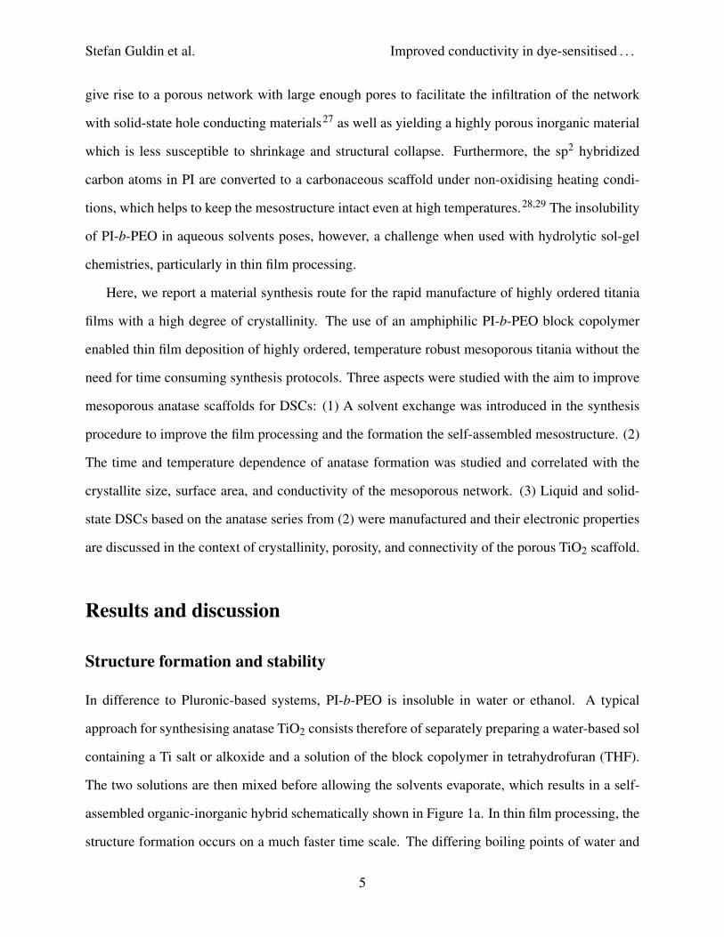
assembled organic-inorganic hybrid schematically shown in Figure 1a. In thin film processing, the
structure formation occurs on a much faster time scale. The differing boiling points of water and
5
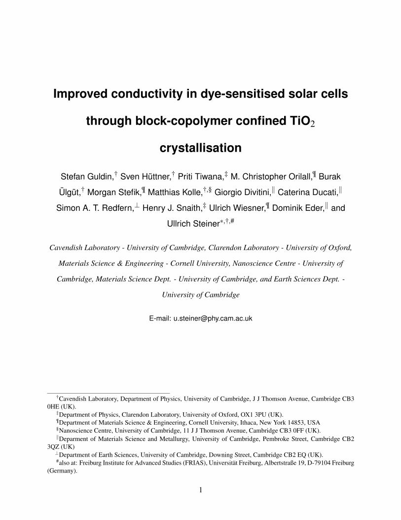
Stefan Guldin et al. Improved conductivity in dye-sensitised . . .
ca
100nm100nm
b
100nm
300nm
d fe
0.0 0.1 0.2 0.3 0.4 0.5 0.6 0.7 0.8
0
200
400
600
inte
nsity*q
2
q [nm-1]
370°C
430°C
630°C
740°C
Figure 1: Film deposition and structural stability. (a) Hydrolytic TiO2 sol when mixed with a PI-b-PEO solution is structure-directed by copolymer self-assembly, giving rise to nanostructured TiO2after high-temperature annealing. (b) Small-angle x-ray scattering (SAXS) spectra for copolymer-derived TiO2 annealed at 370 C (black squares), 430 C (red circles), 630 C (blue diamonds)and 740 C (yellow triangles). The spectra are scaled in intensity to overlap in the 0− 0.1 nm−1
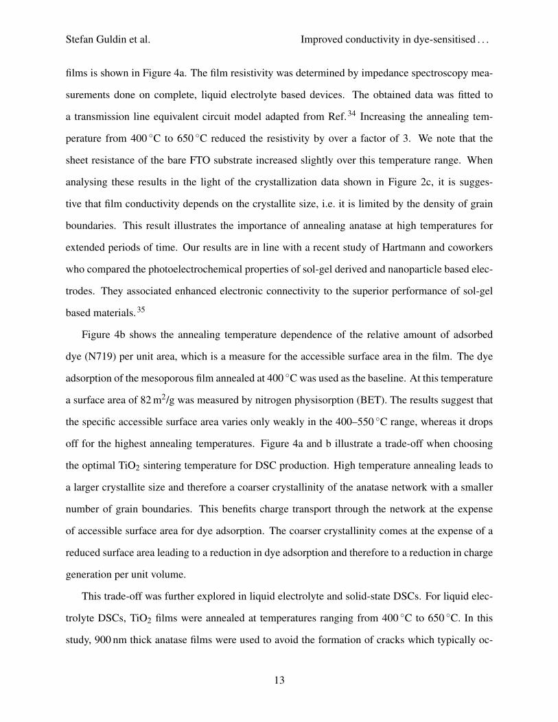
q-range. (c) TEM image of the ordered f.c.c. micellar hybrid film produced by spin-coating theredissolved material. Cross-sectional SEM images of the nanostructured TiO2 films calcined in airat temperatures of (d) 430 C and (e) 690 C for 400 min. (f) Cross-sectional SEM image of a filmannealed at 740 C which resulted in the transformation from anatase to rutile and a subsequentloss of the mesopores.
6
Stefan Guldin et al. Improved conductivity in dye-sensitised . . .
the organic solvents therefore often lead to quenched morphologies with poor structure control. For
high inorganic loadings, the low solubility of polymer in the water rich solvent mixture imposes
another challenge. We have addressed these limitations by adding a solvent exchange step to the
sample preparation procedure. The initial mixture was slowly dried in a Petri dish and the resulting
hybrid material was directly redissolved in a mixture of 1-butanol and toluene in a ratio that allowed
the formation of an azeotrope30(a solvent mixture of equal boiling point). The azeotrope dissolves
both the hydrophilic and hydrophobic phases of the hybrid material while exhibiting a common
high boiling point. This results in a better solubility of the polymer and titania sol and slower
evaporation of the solvents, which gives rise to better ordered local structure and film formation of
the dried hybrid material. Further experimental details about the redisolution step and its effect on
the morphology of resulting films are given in the Supporting Information (SI).
Figure 1 demonstrates the structural control of this approach. The role of the amphiphilic
block copolymer as structure-directing agent, organising the inorganic titania sol in a highly or-
dered network is illustrated in Figure 1a. Structural order after film deposition and during high
temperature annealing was probed by small angle x-ray scattering (SAXS), shown in Figure 1b.
The characteristic length-scale (d-spacing) of the self-assembled structure was 30 nm, shrinking to
27 nm after removal of the organic template for temperatures above 370 C. The first-order peak at
∼ 0.23 nm−1 disappeared only at 740 C, indicating a loss of structural order at this temperature.
Electron microscopy confirmed these observations. Figure 1c shows a TEM image of a hybrid film
before calcination, consistent with a face-centred-cubic (f.c.c.) micellar hybrid assembly. Note
that this film was simply spin-coated from the 1-butanol/toluene solution without further time-
consuming annealing procedures to promote phase separation. Cross-sectional SEM images of
the calcined films in Figure 1 d-e show that the self-assembled morphology remained intact after
calcination at temperatures of (d) 430 C and (e) 690 C for 400 min. The collapse of the pores
observed at 740 C is evidenced by the SEM cross-section in Figure 1f.
A micellar morphology consistent with a short-range f.c.c. order is observed for a number of
different copolymer architectures and sol-loadings. This suggests that the micro-morphology origi-
7
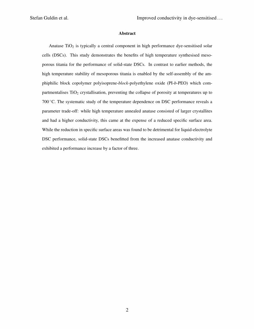
Stefan Guldin et al. Improved conductivity in dye-sensitised . . .
50%
60%
70%
80%
90%
98%
500 550 600 650 7000
50
100
150
200
cry
sta
llisa
tio
ntim
e[m
in]
temperature [°C]
c
d e
20 30 40 50 60 70
0
1000
2000
3000
4000
[220][116]
[204]
[213]
[105] [211]
[200]
[112]
[004]
[103]
inte
nsity
[a.u
]
2theta [°]
[101]
400 450 500 550 600 650 7000
5
10
15
20
me
an
cry
sta
lsiz
e[n
m]
temperature [°C]
a
0 50 100 150 200 250 3000
20
40
60
80
100
120
pe
ak
are
a[in
ten
sity]
time [min]
b
f
24 26 28 30
0
2000
4000
6000
8000
10000
2theta [°]
inte
nsity
[a.u
.]
sol only
2to1
1to1
24 26 28 30
0
2000
4000
6000
2theta[°]
inte
nsity
[a.u
.]
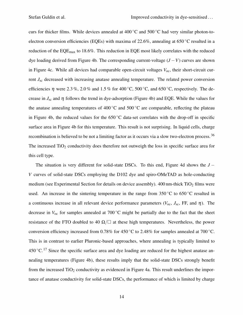
Figure 2: Crystallisation of TiO2 anatase crystals in block-copolymer derived confinement (a)Wide angle x-ray diffraction scans of mesoporous films annealed at 400 C, 500 C, 600 C, and700 C (bottom to top). (b) Anatase (101) crystal footprint as a function of crystallisation tem-perature after annealing for 400 min. From bottom to top: 400 C to 700 C in 50 C increments(structurally intact), and 740 C (collapsed structure). (c) Debye-Scherrer mean crystallite sizesafter annealing for 400 min as a function of temperature. (d) Evolution of crystallinity by monitor-ing the peak area as a function of time at 530 C. (e) Evolution of overall crystallinity with time asa function of temperature. (f) Dependence of anatase (101) peak on mass ratio of TiO2 to blockcopolymer. From bottom to top; black: 1to1 mass ratio (mean crystallite size: 9.5 nm); red: 2to1mass ratio (14.7 nm); blue: sol only (23.6 nm).
nates from the packing structures that probably already exist in solution. In contrast to structure for-
mation in bulk samples produced by drop-casting (where an equilibrated microphase morphology
is observed), spin-cast films are presumably kinetically hindered from forming a self-assembled
morphology dictated by the copolymer architecture in the melt. Supported by our results discussed
below, it is important to note that, despite the micellar assembly a 3D bicontinuous network of
titania and pores is obtained with structure control (through the micellar size) on the 10-nm length
scale. The robustness of the micellar morphology with respect to the various system parameters is
an advantage, simplifying the comparison of differently produced samples.
8
Stefan Guldin et al. Improved conductivity in dye-sensitised . . .
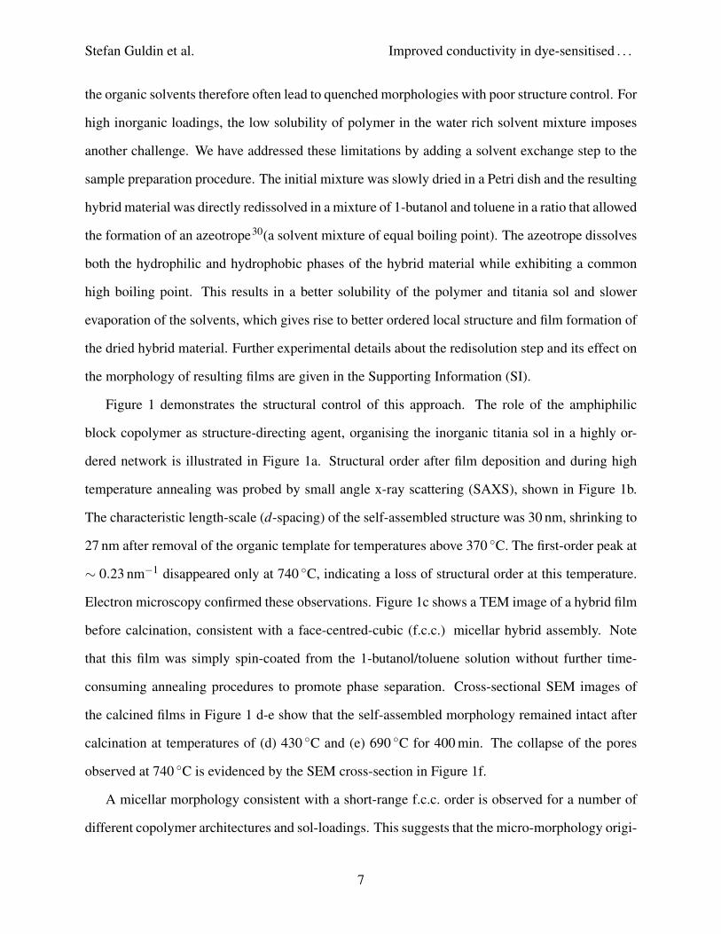
Crystallisation kinetics and crystal sizes
The overall crystallinity and crystallite size strongly influence charge transport properties of poly-
crystalline wide band-gap semiconductors and therefore play important roles in device applica-
tions. Annealing times and temperatures during crystal formation are obviously important in con-
trolling these parameters. Figure 2a shows wide-angle x-ray scattering (WAXS) patterns of TiO2
films annealed for 400 min at temperatures between 400C and 700C. Up to annealing tempera-
tures of 700C, all reflections can be indexed to anatase (PDF 71-1167), confirming phase purity
for these annealing conditions. The smaller angular range of Figure 2b shows the evolution of the
width of the anatase (101) peak with temperature after an annealing time of 400 min. The Debye
Scherrer analysis of the full-width at half maximum (FWHM) of the (101) peak was used to define
the mean crystallite size of the polycrystalline assembly, shown in Figure 2c. The final crystallite
size was found to be independent of the heating rate in the range of 1 – 10 C/min. In contrast to
phase purity up to 700C, a significant rutile content can be observed after annealing at 740C,
evidenced by the appearance of the (110) peak at 27.3 (PDF 76-1940). A comparison of the
SAXS and XRD results of Figure 1b and Figure 2b suggests that the structural collapse at 740 C
is caused by the stresses involved in the reconstructional transformation from anatase to rutile.
To investigate the time required for completion of the crystallisation process, we monitored
the crystallite growth in-situ during the calcination process by x-ray diffraction. The observed
diffraction range for 2θ between 22 and 32 (Cu Kα radiation) contains the anatase (101) peak
which was used for this analysis. A typical in-situ scan of TiO2 during calcination at 530 C is
shown in Figure 2d, indicating completion of the crystallisation process after about 100 min.
The evolution of the overall crystallinity with time was determined by comparing, at each
temperature, the area of the anatase peak with the peak area for an annealing time of 400 min,
which was defined as 100% crystallinity. The result of this analysis is shown in Figure 2e, where
the time required to reach values of the overall crystallinity of 50% - 98% is plotted as a function
of temperature. While near-complete crystallinity (98%) was obtained after 100 – 150 min for
temperatures between 530C and 690C, much longer times were needed for temperatures below
9
Stefan Guldin et al. Improved conductivity in dye-sensitised . . .
500 C. In addition, the careful investigation of all WAXS samples in reflection (Figure 2a and
b) and transmission (shown in the SI) showed no sign of an amorphous hump. Our results agree
with a study by Fattakhova et al. 20 reporting the rapid disappearance of the amorphous signal for
annealing temperatures between 550 C and 650 C. Based on our measurements, we conclude that
the amorphous content in all our samples was very low when annealed above 400 C for several
hours.
The crystal growth kinetics in Figure 2e reveal further details. While the crystallite size of the
fully crystalline material increases with increasing temperature, the time required to reach 98%
crystallinity is a non-monotonous function of temperature. The two minima in the 98% curve in
Figure 2e suggest that several different mechanisms govern the anatase crystallisation kinetics as
a function of temperature. This is, however, not reflected in the final crystal sizes of Figure 2c.
The slow crystallisation for temperatures below 500C is noteworthy because mesoporous TiO2
employed in DSCs is often annealed at similarly low temperatures.
The crystal size is strongly influenced by the confinement of the organic template shown in
Figure 2f for an annealing temperature of 500C. Doubling the weight ratio of polymer to hy-
drolytic sol leads to a decrease in crystallite size by ≈ 30%. In the absence of the organic structure
directing agent much larger crystals (> 23 nm) were observed. In addition, we have recently shown
that the crystallization environment, tuned by the inorganic to organic ratio, is a decisive factor in
determining the distribution of sub-bandgap electronic states and the associated electronic function
in solid-state dye-sensitized solar cells.31
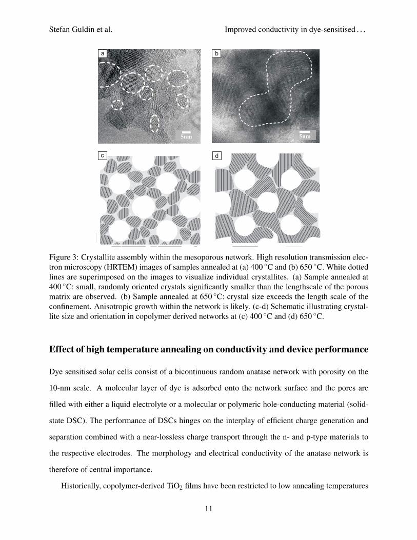
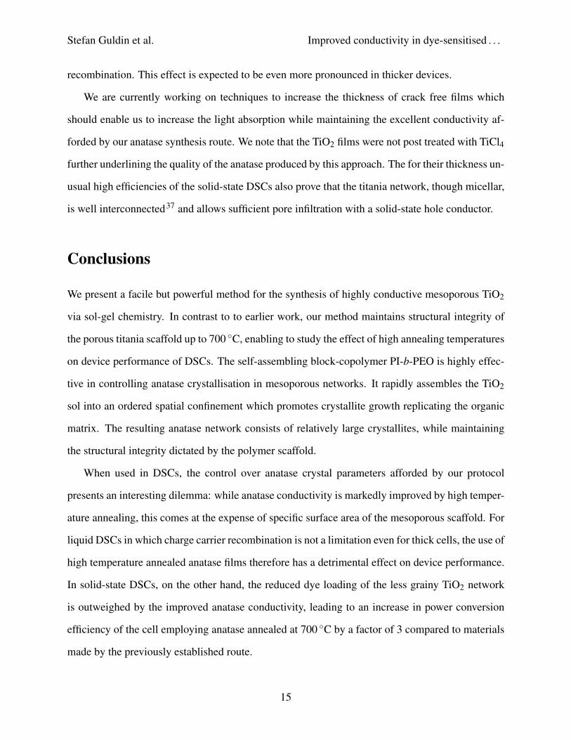
High resolution transmission electron microscopy (HRTEM) images of samples annealed at
400 C and 650 C are shown in Figure 3a and b, respectively. The sample annealed for 400
min at 400 C shows a heterogeneous assembly of small crystallites of 10±5 nm. Increasing the
temperature to 650C, leads to larger and more irregularly shaped crystals of around 20 nm, which
probably derive from the coalescence of smaller grains. These results are consistent with the x-ray
diffraction data analysis. The schematics in Figure 3c and d illustrate crystal growth in copolymer
derived confinement at low and high temperatures, respectively.
10
Stefan Guldin et al. Improved conductivity in dye-sensitised . . .
d
5nm
b
c
5nm
a
5nm
Figure 3: Crystallite assembly within the mesoporous network. High resolution transmission elec-tron microscopy (HRTEM) images of samples annealed at (a) 400 C and (b) 650 C. White dottedlines are superimposed on the images to visualize individual crystallites. (a) Sample annealed at400 C: small, randomly oriented crystals significantly smaller than the lengthscale of the porousmatrix are observed. (b) Sample annealed at 650 C: crystal size exceeds the length scale of theconfinement. Anisotropic growth within the network is likely. (c-d) Schematic illustrating crystal-lite size and orientation in copolymer derived networks at (c) 400 C and (d) 650 C.
Effect of high temperature annealing on conductivity and device performance
Dye sensitised solar cells consist of a bicontinuous random anatase network with porosity on the
10-nm scale. A molecular layer of dye is adsorbed onto the network surface and the pores are
filled with either a liquid electrolyte or a molecular or polymeric hole-conducting material (solid-
state DSC). The performance of DSCs hinges on the interplay of efficient charge generation and
separation combined with a near-lossless charge transport through the n- and p-type materials to
the respective electrodes. The morphology and electrical conductivity of the anatase network is
therefore of central importance.
Historically, copolymer-derived TiO2 films have been restricted to low annealing temperatures
11
Stefan Guldin et al. Improved conductivity in dye-sensitised . . .
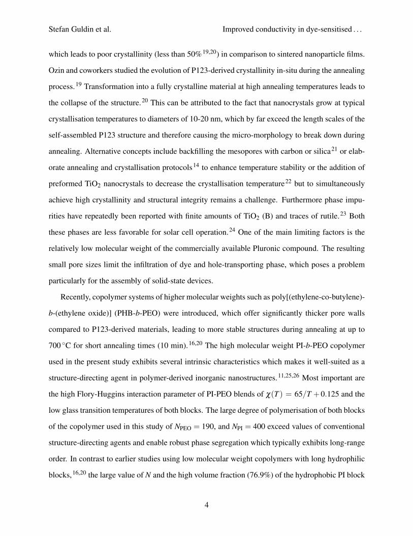
400 450 500 550 600 650
2
4
6
8
10
12
14
16
resis
tivity
[m
]x
10^7
annealing temperature [°C]
a b
c d
400 450 500 550 600 650 7000.0
0.2
0.4
0.6
0.8
1.0
no
rm.
am
ou
nt
of
dye
ad
so
rbe
d
annealing temperature [°C]
0.0 0.2 0.4 0.6 0.80.0
1.0
2.0
3.0
4.0
cu
rre
nt
de
nsity
[mA
/cm
2]
voltage [V]
650°C
500°C
400°C
0.0 0.2 0.4 0.6 0.80.0
1.0
2.0
3.0
4.0
5.0
6.0
cu
rre
nt
de
nsity
[mA
/cm
2]
voltage [V]
700°C
650°C
600°C
550°C
500°C
450°C
350°C
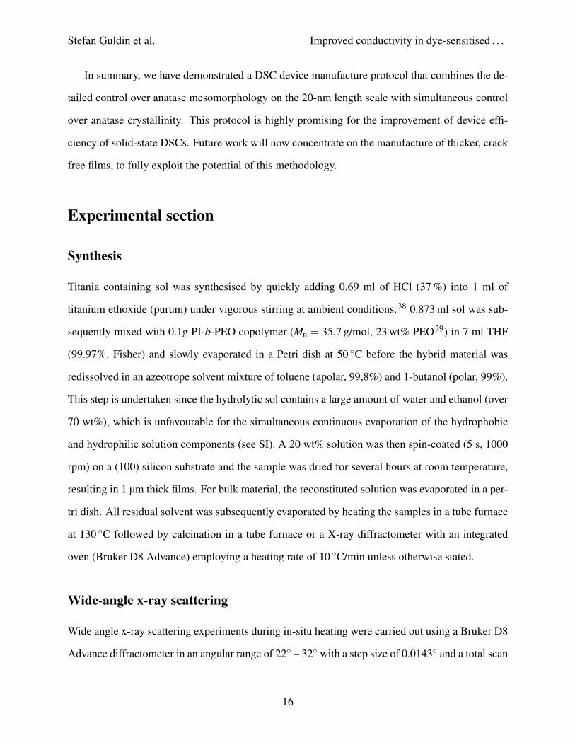
Figure 4: Effects of crystallinity on device performance. (a) Resistivity determined by impedancespectroscopy of 900 nm thick films annealed at 400 C, 500 C, and 650 C. (b) Relative amount ofdye adsorbed per unit area. The dye adsorption of the mesoporous film annealed at 400 C was usedas the baseline. (c) Current-voltage characteristics for liquid electrolyte DSC devices annealedat 400 C, 500 C, and 650 C. (d) solid-state DSC performance of samples annealed at 350 Cto 700 C. Higher temperatures led to a continuous increase in efficiency from 0.8% (450 C)to 2.5% (700 C) for 400 nm thick films sensitised with D102. Liquid and solid-state deviceswere characterised under standardised AM 1.5 illumination of 100 W/cm2. See the supportinginformation for a summary of all photovoltaic device performance parameters.
resulting in films which suffer from high resistivities. Since a low electron mobility has been
identified as a limitation for the development of high-efficiency solid-state DSCs,9 this material
synthesis route is particularly interesting for applications where poor charge carrier transport lim-
its the device performance. Anatase resistivity is expected to depend sensitively on the degree of
crystallinity, crystallite size, and topology of the porous network,32,33 all of which can be con-
trolled by the present approach.
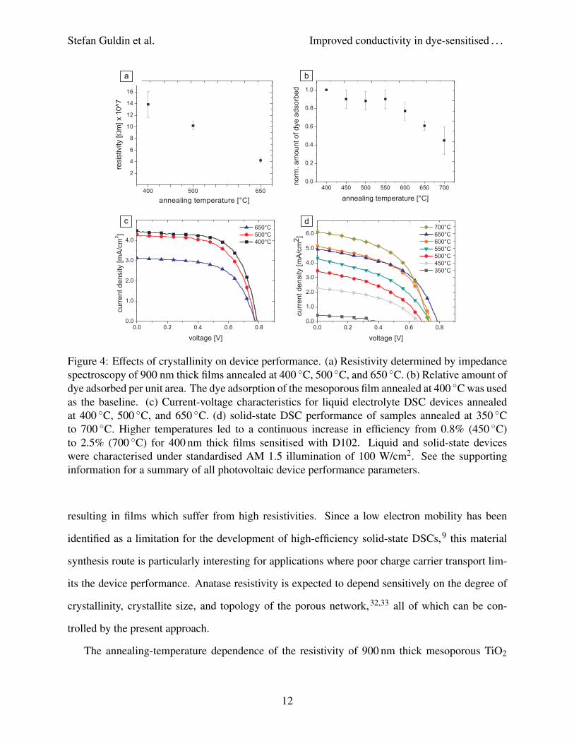
The annealing-temperature dependence of the resistivity of 900 nm thick mesoporous TiO2
12
Stefan Guldin et al. Improved conductivity in dye-sensitised . . .
films is shown in Figure 4a. The film resistivity was determined by impedance spectroscopy mea-
surements done on complete, liquid electrolyte based devices. The obtained data was fitted to
a transmission line equivalent circuit model adapted from Ref.34 Increasing the annealing tem-
perature from 400 C to 650 C reduced the resistivity by over a factor of 3. We note that the
sheet resistance of the bare FTO substrate increased slightly over this temperature range. When
analysing these results in the light of the crystallization data shown in Figure 2c, it is sugges-
tive that film conductivity depends on the crystallite size, i.e. it is limited by the density of grain
boundaries. This result illustrates the importance of annealing anatase at high temperatures for
extended periods of time. Our results are in line with a recent study of Hartmann and coworkers
who compared the photoelectrochemical properties of sol-gel derived and nanoparticle based elec-
trodes. They associated enhanced electronic connectivity to the superior performance of sol-gel
based materials.35
Figure 4b shows the annealing temperature dependence of the relative amount of adsorbed
dye (N719) per unit area, which is a measure for the accessible surface area in the film. The dye
adsorption of the mesoporous film annealed at 400 C was used as the baseline. At this temperature
a surface area of 82 m2/g was measured by nitrogen physisorption (BET). The results suggest that
the specific accessible surface area varies only weakly in the 400–550 C range, whereas it drops
off for the highest annealing temperatures. Figure 4a and b illustrate a trade-off when choosing
the optimal TiO2 sintering temperature for DSC production. High temperature annealing leads to
a larger crystallite size and therefore a coarser crystallinity of the anatase network with a smaller
number of grain boundaries. This benefits charge transport through the network at the expense
of accessible surface area for dye adsorption. The coarser crystallinity comes at the expense of a
reduced surface area leading to a reduction in dye adsorption and therefore to a reduction in charge
generation per unit volume.
This trade-off was further explored in liquid electrolyte and solid-state DSCs. For liquid elec-
trolyte DSCs, TiO2 films were annealed at temperatures ranging from 400 C to 650 C. In this
study, 900 nm thick anatase films were used to avoid the formation of cracks which typically oc-
13
Stefan Guldin et al. Improved conductivity in dye-sensitised . . .
curs for thicker films. While devices annealed at 400 C and 500 C had very similar photon-to-
electron conversion efficiencies (EQEs) with maxima of 22.6%, annealing at 650 C resulted in a
reduction of the EQEmax to 18.6%. This reduction in EQE most likely correlates with the reduced
dye loading derived from Figure 4b. The corresponding current-voltage (J−V ) curves are shown
in Figure 4c. While all devices had comparable open-circuit voltages Voc, their short-circuit cur-
rent Jsc decreased with increasing anatase annealing temperature. The related power conversion
efficiencies η were 2.3 %, 2.0 % and 1.5 % for 400 C, 500 C, and 650 C, respectively. The de-
crease in Jsc and η follows the trend in dye-adsorption (Figure 4b) and EQE. While the values for
the anatase annealing temperatures of 400 C and 500 C are comparable, reflecting the plateau
in Figure 4b, the reduced values for the 650 C data-set correlates with the drop-off in specific
surface area in Figure 4b for this temperature. This result is not surprising. In liquid cells, charge
recombination is believed to be not a limiting factor as it occurs via a slow two-electron process.36
The increased TiO2 conductivity does therefore not outweigh the loss in specific surface area for
this cell type.
The situation is very different for solid-state DSCs. To this end, Figure 4d shows the J −
V curves of solid-state DSCs employing the D102 dye and spiro-OMeTAD as hole-conducting
medium (see Experimental Section for details on device assembly). 400 nm-thick TiO2 films were
used. An increase in the sintering temperature in the range from 350 C to 650 C resulted in
a continuous increase in all relevant device performance parameters (Voc, Jsc, FF, and η). The
decrease in Voc for samples annealed at 700 C might be partially due to the fact that the sheet
resistance of the FTO doubled to 40 Ω/ at these high temperatures. Nevertheless, the power
conversion efficiency increased from 0.78% for 450 C to 2.48% for samples annealed at 700 C.
This is in contrast to earlier Pluronic-based approaches, where annealing is typically limited to
450 C.17 Since the specific surface area and dye loading are reduced for the highest anatase an-
nealing temperatures (Figure 4b), these results imply that the solid-state DSCs strongly benefit
from the increased TiO2 conductivity as evidenced in Figure 4a. This result underlines the impor-
tance of anatase conductivity for solid-state DSCs, the performance of which is limited by charge
14
Stefan Guldin et al. Improved conductivity in dye-sensitised . . .
recombination. This effect is expected to be even more pronounced in thicker devices.
We are currently working on techniques to increase the thickness of crack free films which
should enable us to increase the light absorption while maintaining the excellent conductivity af-
forded by our anatase synthesis route. We note that the TiO2 films were not post treated with TiCl4
further underlining the quality of the anatase produced by this approach. The for their thickness un-
usual high efficiencies of the solid-state DSCs also prove that the titania network, though micellar,
is well interconnected37 and allows sufficient pore infiltration with a solid-state hole conductor.
Conclusions
We present a facile but powerful method for the synthesis of highly conductive mesoporous TiO2
via sol-gel chemistry. In contrast to to earlier work, our method maintains structural integrity of
the porous titania scaffold up to 700 C, enabling to study the effect of high annealing temperatures
on device performance of DSCs. The self-assembling block-copolymer PI-b-PEO is highly effec-
tive in controlling anatase crystallisation in mesoporous networks. It rapidly assembles the TiO2
sol into an ordered spatial confinement which promotes crystallite growth replicating the organic
matrix. The resulting anatase network consists of relatively large crystallites, while maintaining
the structural integrity dictated by the polymer scaffold.
When used in DSCs, the control over anatase crystal parameters afforded by our protocol
presents an interesting dilemma: while anatase conductivity is markedly improved by high temper-
ature annealing, this comes at the expense of specific surface area of the mesoporous scaffold. For
liquid DSCs in which charge carrier recombination is not a limitation even for thick cells, the use of
high temperature annealed anatase films therefore has a detrimental effect on device performance.
In solid-state DSCs, on the other hand, the reduced dye loading of the less grainy TiO2 network
is outweighed by the improved anatase conductivity, leading to an increase in power conversion
efficiency of the cell employing anatase annealed at 700 C by a factor of 3 compared to materials
made by the previously established route.
15
Stefan Guldin et al. Improved conductivity in dye-sensitised . . .
In summary, we have demonstrated a DSC device manufacture protocol that combines the de-
tailed control over anatase mesomorphology on the 20-nm length scale with simultaneous control
over anatase crystallinity. This protocol is highly promising for the improvement of device effi-
ciency of solid-state DSCs. Future work will now concentrate on the manufacture of thicker, crack
free films, to fully exploit the potential of this methodology.
Experimental section
Synthesis
Titania containing sol was synthesised by quickly adding 0.69 ml of HCl (37 %) into 1 ml of
titanium ethoxide (purum) under vigorous stirring at ambient conditions.38 0.873 ml sol was sub-
sequently mixed with 0.1g PI-b-PEO copolymer (Mn = 35.7 g/mol, 23 wt% PEO39) in 7 ml THF
(99.97%, Fisher) and slowly evaporated in a Petri dish at 50 C before the hybrid material was
redissolved in an azeotrope solvent mixture of toluene (apolar, 99,8%) and 1-butanol (polar, 99%).
This step is undertaken since the hydrolytic sol contains a large amount of water and ethanol (over
70 wt%), which is unfavourable for the simultaneous continuous evaporation of the hydrophobic
and hydrophilic solution components (see SI). A 20 wt% solution was then spin-coated (5 s, 1000
rpm) on a (100) silicon substrate and the sample was dried for several hours at room temperature,
resulting in 1 µm thick films. For bulk material, the reconstituted solution was evaporated in a per-
tri dish. All residual solvent was subsequently evaporated by heating the samples in a tube furnace
at 130 C followed by calcination in a tube furnace or a X-ray diffractometer with an integrated
oven (Bruker D8 Advance) employing a heating rate of 10 C/min unless otherwise stated.
Wide-angle x-ray scattering
Wide angle x-ray scattering experiments during in-situ heating were carried out using a Bruker D8
Advance diffractometer in an angular range of 22 – 32 with a step size of 0.0143 and a total scan
16
Stefan Guldin et al. Improved conductivity in dye-sensitised . . .
time of 5 min. A heating rate of 10 C/min was used unless otherwise stated. Samples were mea-
sured during annealing in air for up to 7 hours, representing 84 consecutive x-ray scans. Because of
its crystal orientation, the single crystalline silicon substrate is not expected to contribute to a sig-
nal in the observed angular range. The measurements covered a temperature range between 380 C
and 740 C in intervals of around 50 C . The obtained raw data was corrected for the CuKα2 radi-
ation by the Bruker software EVA. To obtain the peak broadening caused by the size of the anatase
crystalites, a Voigt function was fitted to the peaks. The peak width (full width at half maximum)
of the Lorentzian and the Gaussian parts of the Voigt function were determined by the approxima-
tion of Olivero and Longbothum.40 The peak width was then corrected for machine broadening
by subtracting (by deconvolution) the broadening of a monocrystalline silicon reference sample.
The Debye-Scherrer equation was subsequently employed to obtain a mean crystallite diameter
of the peak broadening41 Like in similar studies, the dimensionless number K = 0.89 was used
as Debye-Scherrer constant.19,42 X-ray diffraction of separately annealed samples was carried out
with a Philips PW1830 Generator 3a.
Small-angle X-ray scattering (SAXS)
Small-angle x-ray scattering of CuKα radiation was collected in transmission geometry at a sample-
detector distance of 1.05 m (Bruker AXS Nanostar, Karlsruhe, Germany). Acquisition times of
7500 s were used. The scattered intensity was collected using a 2-dimensional Hi-Star gas-filled
wire detector with 1024× 1024 channels and the incident beam-path directed towards its centre. A
lead beam-stop was suspended in front of the detector in the beam path, to prevent damage due to
unattenuated X-rays; this obscured any scattering below q = 0.08nm−1. ’Background’ scans were
performed with an empty camera; this was used to correct the scattering measured for specimens,
after allowing for transmission. In each case, the scattering patterns were found to be isotropic (i.e.
no preferred orientation). Radial scattering intensity profiles were obtained by averaging over the
azimuthal angle (from 0 to 360) with 0.005 increments in scattering angle.
17
Stefan Guldin et al. Improved conductivity in dye-sensitised . . .
Transmission electron microscopy (TEM)
Samples annealed at different temperatures were dispersed on holey carbon coated TEM copper
grids and imaged using a FEI Tecnai F20 microscope (200 kV). For high resolution transmission
electron microscopy, a Jeol JEM 4000EX (400 kV) was used.
Impedance spectroscopy
A Gamry Reference 600 potentiostat with the EIS300 software package was employed to measure
impedance spectra. Spectra were collected in the dark under forward bias that is adjusted to match
the open circuit potential under AM 1.5. The AC amplitude used was 10 mV and the spectra were
collected from 10 mHz to 10 kHz with 10 frequencies per decade. The analysis of the spectra were
performed using ZView v2.8 using a circuit model adapted from Ref.34
Dye absorption measurements
In order to quantify the accessible surface area for dye sensitization, dye desorption studies were
carried out similar to Neale et al.43 Mesoporous TiO2 films were immersed in a 0.5 mM solution
of cis-di(thiocyanato)-bis(2,2’-bipyridyl-4-carboxylate-4’-carboxylic acid)-ruthenium(II) (termed
N719) in a mixture of acetonitrile:tert-butyl alcohol (volume ratio 1:1) and kept in the dark for 16
hours at room temperature. The samples were then thoroughly rinsed with acetonitrile and subse-
quently submerged into a 1.0 mM KOH solution (3 ml) for 3 hours to fully desorb the dye. The
absorbance of the resulting light pink solutions was measured with an UV-vis spectrophotometer
(HP 8453 UV/vis spectrophotometer, wavelength range 190 – 1100 nm, 1 nm slit width, 0.03%
stray light). The relative amount of dye adsorbed was determined by comparing the peak height of
the respective solution with the reference obtained from desorption of the film annealed at 400 C.
18
Stefan Guldin et al. Improved conductivity in dye-sensitised . . .
Liquid electrolyte DSC assembly
Fluorine doped SnO2 (FTO) coated glass sheets (Nipon Sheet Glass, TEC15) were manually
cleaned with Hellmanex soap, acetone, and isopropanol followed by 10 min in an O2 plasma etcher.
900 nm thick anatase films were then spin-cast onto the substrates and annealed as described above.
The samples were sensitised with N719 as described above.
The counter electrodes used for these devices were sheets of pre-drilled platinized FTO glass.
The platinization was carried out by coating the FTO with hexachloroplatinic (IV) acid from an
anhydrous isopropanol solution (50 mM) followed by heating to 450 C for 15 min. The dyed TiO2
electrodes were washed in acetonitrile, dried and assembled in a sandwich type cell configuration
with the platinized counter electrodes, using a ‘hot-melt’ 50 µm thick surlyn spacer (Dupont) to
seal the working and counter electrode together. A drop of ‘Robust’ liquid electrolyte (0.8 M
PMII, 0.15 M iodine, 0.1 M GuNCS, and 0.5 M NMBI in 3-methoxypropionitrile)44 was dispensed
into a hole in the counter electrode and the cell was filled via vacuum backfilling and sealed with
polyimide tape (Dupont).
Solid-state DSC assembly
Solid-state DSCs were fabricated using the method outlined in Ref.45 The TiO2 films were dye-
sensitized with D102 (indolin-based organic dye) for 1 hour. Spiro-OMeTAD (2,2’,7,7’-tetrakis(N,N-
di-methoxyphenyamine)-9,9’-spirobifluorene) dissolved in chlorobenzene was used as the hole-
transporting material (HTM), with tert-butyl pyridine (tBP) and bis(trifluoromethyl-sulfonyl)amine
lithium salt (Li-TFSI) (dissolved separately in acetonitrile) used as additives for improved device
performance.45 Finally, 150 nm thick silver electrodes were evaporated over the HTM layer under
high vacuum (10−6 mbar) to complete the devices.
19
Stefan Guldin et al. Improved conductivity in dye-sensitised . . .
DSC characterisation
The solar cells were measured under AM 1.5 simulated sun light generated by a 300 W Oriel so-
lar simulator. The power of the simulated light was measured using a calibrated Si photo diode
(Fraunhofer Institute for Solar Energy Systems). The mismatch factor to the solar spectrum was
calculated over the entire spectral response region of both the test solar cells and calibration diode
following the method of Seaman.46 The active area of the DSCs was 0.13 cm2. The current-voltage
measurements were recorded by a Keithley 237 sourcemeter connected to a computer.
Acknowledgement
This work was funded in part by by the EPSRC Nanotechnology Grand Challenges Energy grant
(EP/F056702/1), and EP/F065884/1, the Department of Energy (DE-FG02 87ER45298) through
the Cornell Fuel Cell Institute (CFCI), the National Science Foundation (DMR-0605856), and the
Cornell Universiy KAUST Center for Research and Education. SG acknowledges support by the
Studienstiftung des deutschen Volkes and CD thanks the Royal Society for funding. We thank T.
Abraham for help with the XRD measurements, P. Laity for help with SAXS measurements, and
P. Müller-Buschbaum for useful discussions.
References
(1) O‘Regan, B.; Grätzel, M. Nature 1991, 353, 737–740.
(2) Linsebigler, A.; Lu, G.; Yates, J. Chemical Reviews 1995, 95, 735–758.
(3) Brezesinski, T.; Wang, J.; Polleux, J.; Dunn, B.; Tolbert, S. H. Journal Of The American
Chemical Society 2009, 131, 1802–1809.
(4) Varghese, O.; Gong, D.; Paulose, M.; Ong, K.; Grimes, C. Sensors And Actuators B-Chemical
2003, 93, 338–344, 9th International Meeting on Chemical Sensors (IMCS-9), BOSTON,
MASSACHUSETTS, JUL 07-10, 2002.
20
Stefan Guldin et al. Improved conductivity in dye-sensitised . . .
(5) Bonhote, P.; Gogniat, E.; Campus, F.; Walder, L.; Gratzel, M. Displays 1999, 20, 137–144.
(6) Burnside, S.; Shklover, V.; Barbe, C.; Comte, P.; Arendse, F.; Brooks, K.; Gratzel, M. Chem-
istry Of Materials 1998, 10, 2419–2425.
(7) Dittrich, T.; Lebedev, E.; Weidmann, J. Physica Status Solidi 1998, 165, R5–R6.
(8) Tiwana, P.; Parkinson, P.; Johnston, M. B.; Snaith, H. J.; Herz, L. M. Journal Of Physical
Chemistry C 2010, 114, 1365–1371.
(9) Snaith, H. J.; Grätzel, M. Advanced Materials 2007, 19, 3643+.
(10) Schmidt-Mende, L.; Grätzel, M. Thin Solid Films 2006, 500, 296–301.
(11) Templin, M.; Franck, A.; DuChesne, A.; Leist, H.; Zhang, Y.; Ulrich, R.; Schadler, V.; Wies-
ner, U. Science 1997, 278, 1795–1798.
(12) Zhao, D.; Feng, J.; Huo, Q.; Melosh, N.; Fredrickson, G.; Chmelka, B.; Stucky, G. Science
1998, 279, 548–552.
(13) Yang, P.; Zhao, D.; Margolese, D.; Chmelka, B.; Stucky, G. Nature 1998, 396, 152–155.
(14) Crepaldi, E.; Soler-Illia, G.; Grosso, D.; Cagnol, F.; Ribot, F.; Sanchez, C. Journal Of The
American Chemical Society 2003, 125, 9770–9786.
(15) Choi, S.; Mamak, M.; Coombs, N.; Chopra, N.; Ozin, G. Advanced Functional Materials
2004, 14, 335–344.
(16) Smarsly, B.; Grosso, D.; Brezesinski, T.; Pinna, N.; Boissiere, C.; Antonietti, M.; Sanchez, C.
Chemistry Of Materials 2004, 16, 2948–2952.
(17) Zukalova, M.; Zukal, A.; Kavan, L.; Nazeeruddin, M.; Liska, P.; Grätzel, M. Nano Letters
2005, 5, 1789–1792.
21
Stefan Guldin et al. Improved conductivity in dye-sensitised . . .
(18) Wei, M.; Konishi, Y.; Zhou, H.; Yanagida, M.; Sugihara, H.; Arakawa, H. Journal Of Mate-
rials Chemistry 2006, 16, 1287–1293.
(19) Choi, S.; Mamak, M.; Speakman, S.; Chopra, N.; Ozin, G. Small 2005, 1, 226–232.
(20) Fattakhova-Rohlfing, Dina and Wark, Michael and Brezesinski, Torsten and Smarsly, Bernd
M. and Rathousky, Jiri, Advanced Functional Materials 2007, 17, 123–132.
(21) Kondo, J. N.; Domen, K. Chemistry Of Materials 2008, 20, 835–847.
(22) Szeifert, J. M.; Fattakhova-Rohlfing, D.; Georgiadou, D.; Kalousek, V.; Rathouský, J.;
Kuang, D.; Wenger, S.; Zakeeruddin, S. M.; GraÌLtzel, M.; Bein, T. Chemistry of Materi-
als 2009, 21, 1260–1265.
(23) Frindell, K.; Bartl, M.; Robinson, M.; Bazan, G.; Popitsch, A.; Stucky, G. Journal Of Solid
State Chemistry 2003, 172, 81–88.
(24) Kartini, I.; Menzies, D.; Blake, D.; da Costa, J.; Meredith, P.; Riches, J.; Lu, G. Journal Of
Materials Chemistry 2004, 14, 2917–2921.
(25) Floudas, G.; Ulrich, R.; Wiesner, U. Journal Of Chemical Physics 1999, 110, 652–663.
(26) Renker, S.; Mahajan, S.; Babski, D.; Schnell, I.; Jain, A.; Gutmann, J.; Zhang, Y.; Gruner, S.;
Spiess, H.; Wiesner, U. Macromolecular Chemistry and Physics 2004, 205, 1021–1030.
(27) Nedelcu, M.; Lee, J.; Crossland, E. J. W.; Warren, S. C.; Orilall, M. C.; Guldin, S.; Huet-
tner, S.; Ducati, C.; Eder, D.; Wiesner, U.; Steiner, U.; Snaith, H. J. Soft Matter 2009, 5,
134–139.
(28) Lee, J.; Orilall, M. C.; Warren, S. C.; Kamperman, M.; Disalvo, F. J.; Wiesner, U. Nature
Materials 2008, 7, 222–228.
22
Stefan Guldin et al. Improved conductivity in dye-sensitised . . .
(29) Nedelcu, M.; Guldin, S.; Orilall, M. C.; Lee, J.; Huettner, S.; Crossland, E. J. W.; War-
ren, S. C.; Ducati, C.; Laity, P. R.; Eder, D.; Wiesner, U.; Steiner, U.; Snaith, H. J. Journal Of
Materials Chemistry 2010, 20, 1261–1268.
(30) Ponton, J. Azeotrope Databank http://www.chemeng.ed.ac.uk/people/jack/azeotrope/.
(31) Docampo, P.; Guldin, S.; Stefik, M.; Tiwana, P.; Orilall, M. C.; Hüttner, S.; Sai, H.; Wies-
ner, U.; Steiner, U.; Snaith, H. J. Advanced Functional Materials 2010, 20, 1787–1796.
(32) Dittrich, T.; Weidmann, J.; Koch, F.; Uhlendorf, I.; Lauermann, I. Applied Physics Letters
1999, 75, 3980–3982.
(33) Benkstein, K.; Kopidakis, N.; van de Lagemaat, J.; Frank, A. Journal Of Physical Chemistry
B 2003, 107, 7759–7767.
(34) Wang, Q.; Ito, S.; Graetzel, M.; Fabregat-Santiago, F.; Mora-Sero, I.; Bisquert, J.; Bessho, T.;
Imai, H. Journal Of Physical Chemistry B 2006, 110, 25210–25221.
(35) Hartmann, P.; Lee, D.-k.; Smarsly, B. M.; Janek, J. ACS Nano 2010, 4, 3147–3154.
(36) Duffy, N.; Peter, L.; Rajapakse, R.; Wijayantha, K. Journal Of Physical Chemistry B 2000,
104, 8916–8919.
(37) Deng, Y.; Yu, T.; Wan, Y.; Shi, Y.; Meng, Y.; Gu, D.; Zhang, L.; Huang, Y.; Liu, C.; Wu, X.;
Zhao, D. Journal Of The American Chemical Society 2007, 129, 1690–1697.
(38) Alberius, P.; Frindell, K.; Hayward, R.; Kramer, E.; Stucky, G.; Chmelka, B. Chemistry Of
Materials 2002, 14, 3284–3294.
(39) Allgaier, J.; Poppe, A.; Willner, L.; Richter, D. Macromolecules 1997, 30, 1582–1586.
(40) Olivero, J.; Longbothum, R. Journal Of Quantitative Spectroscopy & Radiative Transfer
1977, 17, 233–236.
23
Stefan Guldin et al. Improved conductivity in dye-sensitised . . .
(41) Scherrer, P. Nachrichten von der Gesellschaft der Wissenschaften zu Goettingen,
mathematisch-physikalische Klasse 1918, 98–100.
(42) Eder, D.; Windle, A. H. Advanced Materials 2008, 20, 1787+.
(43) Neale, N.; Kopidakis, N.; van de Lagemaat, J.; Gratzel, M.; Frank, A. Journal Of Physical
Chemistry B 2005, 109, 23183–23189.
(44) Kuang, D.; Ito, S.; Wenger, B.; Klein, C.; Moser, J.; Humphry-Baker, R.; Zakeeruddin, S.;
Grätzel, M. Journal Of The American Chemical Society 2006, 128, 4146–4154.
(45) Snaith, H. J.; Schmidt-Mende, L.; Gratzel, M.; Chiesa, M. Physical Review B 2006, 74, year.
(46) Seaman, C. Solar Energy 1982, 29, 291–298.
24