shintaro ueno, naohiro hitachi and shinobu fujihara*shinobu/ijnp00402-0308fujihara.pdf ·...
TRANSCRIPT
Int. J. Nanoparticles, Vol. 4, Nos. 2/3, 2011 231
Copyright © 2011 Inderscience Enterprises Ltd.
Nanostructural control of ZnO photoelectrodes for enhancing solar energy conversion efficiency in dye-sensitised solar cells
Shintaro Ueno, Naohiro Hitachi and Shinobu Fujihara* Department of Applied Chemistry, Faculty of Science and Technology, Keio University, Yokohama 223-8522, Japan E-mail: [email protected] E-mail: [email protected] E-mail: [email protected] *Corresponding author
Abstract: Dye-sensitised solar cells (DSSCs) are one of the promising photovoltaic devices based on nanosized metal oxide semiconductors. We have focused on ZnO photoelectrodes and their nanostructural control in terms of nanomaterials processing. Since significant photophysical and electrochemical reactions take place around electrodes in the operation of DSSCs, their performance depends greatly on nanostructure of photoelectrodes. In this review article, we introduce our series of studies on nanostructural control of ZnO photoelectrodes to enhance the cell performance. It is shown that the introduction of macroporous ZnO particles as light scattering layers is effective to improve the light harvesting efficiency. Formation of silica nanolayers on ZnO electrodes is also proven to be beneficial to suppress the recombination of photogenerated electrons and enhance the charge collection efficiency. In both cases, short-circuit photocurrent density and open-circuit photovoltage were increased and hence, light-to-electricity conversion efficiency could be enhanced up to 4.80% only by controlling the photoelectrode structures.
Keywords: dye-sensitised solar cells; DSSCs; photoelectrodes; photocurrent; photovoltage; zinc oxide; thick film; nanostructure; light scattering; nanocoating; spray drying method; sol-gel method.
Reference to this paper should be made as follows: Ueno, S., Hitachi, N. and Fujihara, S. (2011) ‘Nanostructural control of ZnO photoelectrodes for enhancing solar energy conversion efficiency in dye-sensitised solar cells’, Int. J. Nanoparticles, Vol. 4, Nos. 2/3, pp.231–247.
Biographical notes: Shintaro Ueno received his Masters in Integrated Design Engineering from Keio University in 2010. Currently, he is a PhD student at Keio University and studying nanomaterials science for photoelectrochemical devices.
Naohiro Hitachi received his BS in Applied Chemistry from Keio University in 2009. He is now a graduate school student at Keio University and studying macroporous semiconductor particles for application to photoelectrodes.
232 S. Ueno et al.
Shinobu Fujihara received his PhD in Molecular Engineering from Kyoto University, Japan, in 1995. He has been working at Keio University since then and is now an Associate Professor. He was also a Visiting Scholar at RWTH Aachen University of Technology, Germany, from 2001 to 2002. His main research fields include sol-gel processing of nanomaterials, optical design and synthesis of luminescent materials, wet chemical processing of inorganic fluoride materials, and nanostructural control of metal oxide semiconductors for photoelectrochemical devices.
1 Introduction
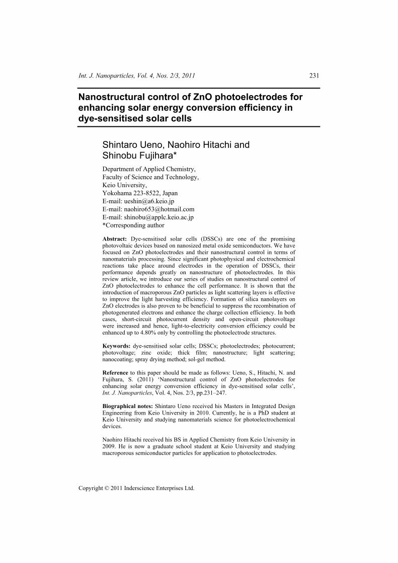
Many kinds of photovoltaic devices have been proposed and actually developed so far using semiconducting materials. Among them, dye-sensitised solar cells (DSSCs) are unique in that they utilise wide-gap metal oxide semiconductors as photoelectrodes. DSSCs are expected as promising alternatives to conventional silicon-based solar cells because of their lower manufacturing cost, possibly higher energy conversion efficiency, and designable features (Grätzel, 2005). DSSCs absorb light by organic or metal-organic complex dyes in their operation and a fundamental cell structure is different from that of solar cells of other kinds. Common DSSCs are composed of a conductive transparent glass substrate, a metal oxide semiconductor layer, sensitising dyes chemically bonded to metal oxides, a liquid electrolyte, and a counter electrode (Figure 1). An assembly of a conductive glass substrate and a dye-sensitised n-type semiconductor layer is called a photoanode, which is an essential part of DSSCs. O’Regan and Grätzel (1991) applied porous TiO2 films to photoanodes and achieved higher energy conversion efficiency, which triggered intensive researches on DSSCs later.
The operation of DSSCs is started with the light absorption by dyes. Excited electrons in dyes are immediately injected to the conduction band of the semiconductor and diffuse throughout a semiconductor layer. The electrons are extracted from the semiconductor layer to an external circuit through a conductive glass substrate. Oxidised dyes are reduced by I–/I3
– redox couples, which receive electrons from a counter electrode, in an electrolyte. Since there are many photophysical and electrochemical reactions taking place around photoelectrodes, the performance of DSSCs depends greatly on their microstructures especially in nanoscale. A nanostructural control of photoelectrodes is then indispensable for enhancing the cell performance effectively. The following guidelines have been widely accepted in designing nanostructures of photoelectrodes:
1 the photoelectrode should have a large specific surface area so that it can be loaded with dyes as many as possible to absorb the incident sunlight effectively
2 continuous networks in semiconductor layers should be developed for effective transportation of injected electrons
3 macroscopic pores should exist in semiconductor layers for accelerated diffusion of redox couples to reduce oxidised dyes inside the photoelectrode.
Nanostructural control of ZnO photoelectrodes 233
Figure 1 The structure of DSSCs (see online version for colours)
The first one is related with efficiency for absorbing sunlight (the light harvesting efficiency). The second and the third one are related with efficiency for collecting photogenerated electrons (the charge collection efficiency). Under these requirements, thick films consisting of semiconductor particles several tens of nanometres in size are exclusively employed in photoelectrodes of DSSCs.
Now, many kinds of metal oxide semiconductors have been investigated as electrode materials such as TiO2, ZnO, SnO2, Nb2O5, WO3, In2O3, and so on (Sayama et al., 1998; Jose et al., 2009). Among these materials, TiO2 is commonly used as dye-sensitised electrodes because porous TiO2 films exhibit relatively high light-to-electricity conversion efficiency in DSSCs. In our series of studies on DSSCs, we have focused our attention on ZnO electrodes as the alternative to TiO2 electrodes. ZnO is an n-type, wide-gap semiconductor of which the band structure is similar to that of TiO2. In fact, ZnO has the similar band gap energy to TiO2 and the conduction band edge energies (ECB) of ZnO and TiO2 are located at the approximately same level (Grätzel, 2001). ZnO electrodes are therefore expected to show conversion efficiency as high as that of TiO2 electrodes. Additionally, the electron mobility of ZnO is much higher than that of TiO2 (Chou et al., 2007), which implies that ZnO may be more appropriate for use in DSSC electrodes.
Actually, however, conversion efficiency has been reportedly around 4% in most of DSSCs using ZnO electrodes, which are far from TiO2 electrodes exhibiting over 11% efficiency. Some specific problems have been clarified in ZnO photoelectrodes. First, ZnO is slightly dissolved and resulting Zn2+ ions easily form complexes with acidic dyes in a dye-loading procedure (Bauer et al., 2001). Dye-loading should then be carried out with a short period of time to prevent the dissolution of ZnO electrodes (Chou et al., 2007), which in turn limits an amount of effectively adsorbed dyes. Second, the recombination of photogenerated electrons seems to occur more frequently in ZnO electrodes, which deteriorates the cell performance especially in an open-circuit voltage
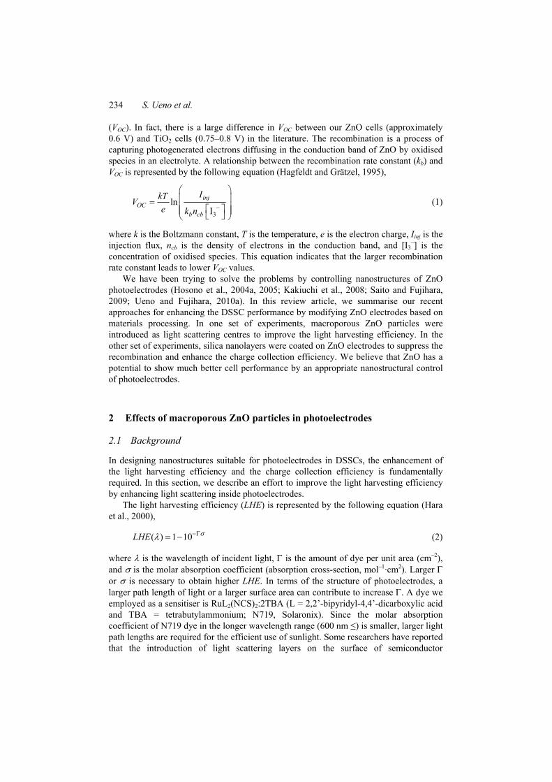
234 S. Ueno et al.
(VOC). In fact, there is a large difference in VOC between our ZnO cells (approximately 0.6 V) and TiO2 cells (0.75–0.8 V) in the literature. The recombination is a process of capturing photogenerated electrons diffusing in the conduction band of ZnO by oxidised species in an electrolyte. A relationship between the recombination rate constant (kb) and VOC is represented by the following equation (Hagfeldt and Grätzel, 1995),
3
lnI
injOC
b cb
IkTVe k n −
⎛ ⎞⎜ ⎟= ⎜ ⎟⎡ ⎤⎜ ⎟⎣ ⎦⎝ ⎠
(1)
where k is the Boltzmann constant, T is the temperature, e is the electron charge, Iinj is the injection flux, ncb is the density of electrons in the conduction band, and [I3
–] is the concentration of oxidised species. This equation indicates that the larger recombination rate constant leads to lower VOC values.
We have been trying to solve the problems by controlling nanostructures of ZnO photoelectrodes (Hosono et al., 2004a, 2005; Kakiuchi et al., 2008; Saito and Fujihara, 2009; Ueno and Fujihara, 2010a). In this review article, we summarise our recent approaches for enhancing the DSSC performance by modifying ZnO electrodes based on materials processing. In one set of experiments, macroporous ZnO particles were introduced as light scattering centres to improve the light harvesting efficiency. In the other set of experiments, silica nanolayers were coated on ZnO electrodes to suppress the recombination and enhance the charge collection efficiency. We believe that ZnO has a potential to show much better cell performance by an appropriate nanostructural control of photoelectrodes.
2 Effects of macroporous ZnO particles in photoelectrodes
2.1 Background
In designing nanostructures suitable for photoelectrodes in DSSCs, the enhancement of the light harvesting efficiency and the charge collection efficiency is fundamentally required. In this section, we describe an effort to improve the light harvesting efficiency by enhancing light scattering inside photoelectrodes.
The light harvesting efficiency (LHE) is represented by the following equation (Hara et al., 2000),
( ) 1 10LHE σλ −Γ= − (2)
where λ is the wavelength of incident light, Γ is the amount of dye per unit area (cm–2), and σ is the molar absorption coefficient (absorption cross-section, mol–1·cm2). Larger Γ or σ is necessary to obtain higher LHE. In terms of the structure of photoelectrodes, a larger path length of light or a larger surface area can contribute to increase Γ. A dye we employed as a sensitiser is RuL2(NCS)2:2TBA (L = 2,2’-bipyridyl-4,4’-dicarboxylic acid and TBA = tetrabutylammonium; N719, Solaronix). Since the molar absorption coefficient of N719 dye in the longer wavelength range (600 nm ≤) is smaller, larger light path lengths are required for the efficient use of sunlight. Some researchers have reported that the introduction of light scattering layers on the surface of semiconductor

Nanostructural control of ZnO photoelectrodes 235
nanoparticle layers is effective for extending the light path (Figure 2) (Wang et al., 2004). Such scattering layers usually consist of larger ZnO particles a few hundreds of nanometres in size and confine the incident light by the back scattering (Saito and Fujihara, 2008). However, these particles used for the light scattering layers have relatively small specific surface areas, which would reduce an amount of adsorbed dye. Hence, we have proposed the use of ZnO particles having new nanostructural features (aggregated particles or macroporous particles) as scattering layers, which has already been proved to be effective in TiO2-based DSSCs (Hitachi and Fujihara, 2010).
Scanning electron microscopy (SEM) images of aggregated ZnO particles and macroporous ZnO particles, which were actually used in our study, are shown in Figure 3. The aggregated ZnO particles are in a spherical shape and consist of ZnO nanoparticles several tens of nanometres in size. The macroporous ZnO particles are similar to the aggregated ZnO particles but have macropores introduced by spherical organic templates (Iskandar et al. 2007). Moreover, the diameter of both the secondary particles is larger than 1 μm, which can act as light scattering centres for the longer wavelength light.
Figure 2 A schematic of DSSCs with light scattering layers in the photoelectrode (see online version for colours)
Figure 3 SEM images of (a) the aggregated ZnO particles (b) the macroporous ZnO particles
236 S. Ueno et al.
2.2 Experimental
Both of the aggregated and the macroporous ZnO particles were fabricated by a spray drying method with a spay dryer (ADL 310, Yamato Scientific Co., Ltd., Japan). For the aggregated ZnO particles, 0.5 g of commercial ZnO nanopowders (Sakai Chemical Industry Co., Ltd., Japan) 20 nm in diameter were dispersed in 100 ml of water and were introduced into the spray dryer. Solid powders were collected through the spray drying at 200ºC. The resultant powders were calcined at 500ºC for 30 min with a heating rate of 5ºC/min. Macroporous particles were fabricated by the same way using colloid suspensions containing 0.5 g of ZnO nanopowders, 100 ml of water, and 1 ml of PS latex (PSL; d = 200 nm, 10% w/w, Duke Scientific Co., USA). PSL works as organic templates to form macropores.
To obtain photoelectrodes, ZnO nanoparticle layers were fabricated first by a doctor blade method. ZnO pastes composed of 0.624 g of ZnO nanopowders, 2 ml of ethanol, 1 ml of water, and 30 μL of acetic acid were mixed thoroughly by stirring for 60 min with the assistance of ultrasonication using an ultrasonic stirrer (USS-1, Nihonseiki Kaisha Ltd., Japan). The resultant pastes were printed onto fluorine-doped tin oxide coated glass substrates (FTO substrates, Nippon Sheet Glass Co., Ltd., Japan; sheet resistance of 10 Ω/square) with mould of plastic tapes (180 μm in thickness) and dried at 90ºC for 30 min.
Light scattering layers were stacked on the underlying nanoparticle layers. We employed three types of particles for light scattering layers; namely, large ZnO particles (d = 600 nm, Sakai), the aggregated ZnO particles, and the macroporous ZnO particles. ZnO pastes were then prepared by using each kind of particles for printing. Compositions of the ZnO pastes for the scattering layers are listed in Table 1. The pastes were thoroughly mixed and printed on the nanoparticle layers with the mould of mending tapes (58 μm in thickness) by the doctor blade method. The layered ZnO thick films obtained were dried at 90ºC for 30 min. The films were heated at 450ºC for 10 min in air. Finally, dye-loading was carried out by immersing the ZnO films in a 0.3 mM N719 ethanolic solution at 60ºC for 90 min. Table 1 Composition of the ZnO pastes used for printing light scattering layers
Paste ZnO particles [g] Ethanol [ml] Water [ml] PEG [g]
Large ZnO 0.624 2.0 1.0 0.624 Aggregated ZnO 0.200 1.0 0.5 0.200 Macroporous ZnO 0.200 1.0 0.5 0.200
Note: Polyethylene glycol (PEG) was employed to enhance the dispersion of the particles.
The morphology of the ZnO electrodes was observed by SEM (S-4700, Hitachi). Optical transmittance and reflectance spectra for the dye-sensitised ZnO photoelectrodes were measured by a UV-vis-NIR spectrophotometer (V-670, JASCO).
For measurements of photocurrent density (J) and photovoltage (V), sandwich-type open cells were constructed with the ZnO/N719 photoanode, the I–/I3
– redox couple electrolyte, a spacer film, and a platinum counter electrode. The electrolyte was composed of 0.1 M LiI, 50 mM I2, 0.6 M 1,2-dimethyl-1,3-propylimidazolium iodide, 1 M tertbutylpyridine, and 3-methoxypropionitrile. The characteristic values, VOC, JSC (short-circuit photocurrent density), ff (fill factor), and η (overall light-to-electricity
Nanostructural control of ZnO photoelectrodes 237
conversion efficiency), were determined from the J–V measurements. The active cell area was 0.25 cm2 regulated by a mask. A 500 W Xe lamp (UXL-500SX, Ushio) was used as the light source to produce the AM 1.5 illumination at 100 mW cm–2 (1 sun). An AM 1.5 filter, a water filter, and an infrared cut filter (S76-HA50, Hoya) were placed in the light path to regulate light in the wavelength range of 300–800 nm and reduce the mismatch between the simulated sunlight and AM 1.5.
The amount of dyes adsorbed on the electrodes was determined by removing them in a 0.5 M NaOH ethanol/water solution. The absorbance of the resultant dye solutions was measured by the spectrophotometer and calibrated with a standard solution of N719.
2.3 Results and discussion
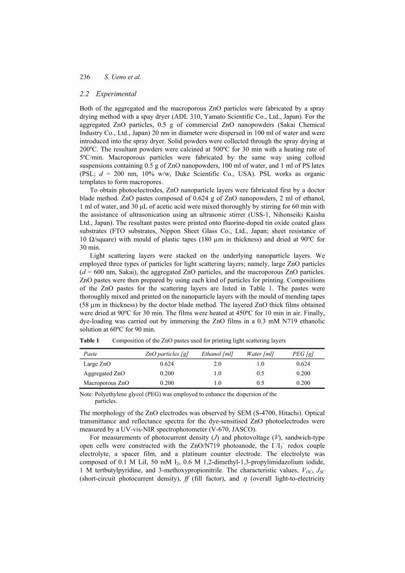
As already mentioned above, each particle fabricated by the spray drying method and subsequent heating is composed of the ZnO nanoparticles several tens of nanometres in size (see Figure 3). The macroporous particles have relatively large pores 100–200 nm in diameter. The pores are assumed to be formed by the combustion of polystyrene (PS) spheres because the pore size corresponds nearly to the PS sphere size.
Figure 4 Cross-sectional SEM images of the electrode (a) N (b) L (c) A (d) M
Four types of ZnO thick films were fabricated in this work; a film only with nanoparticle layers (designated electrode N), a film with the large (d = 600 nm) particle layer on the underlying nanoparticle layer (electrode L), a film with the aggregated particle layer on the underlying nanoparticle layer (electrode A), and a film with the macroporous particle layer on the underlying nanoparticle layer (electrode M). Figure 4 shows cross-sectional SEM images of the resultant layered ZnO thick films used for photoelectrodes. The total
238 S. Ueno et al.
thickness of the films was adjusted to be almost the same. The thickness of the light scattering layer was 5.3, 8.4, and 5.5 μm in the electrode L [Figure 4(b)], the electrode A [Figure 4(c)], and the electrode M [Figure 4(d)], respectively.
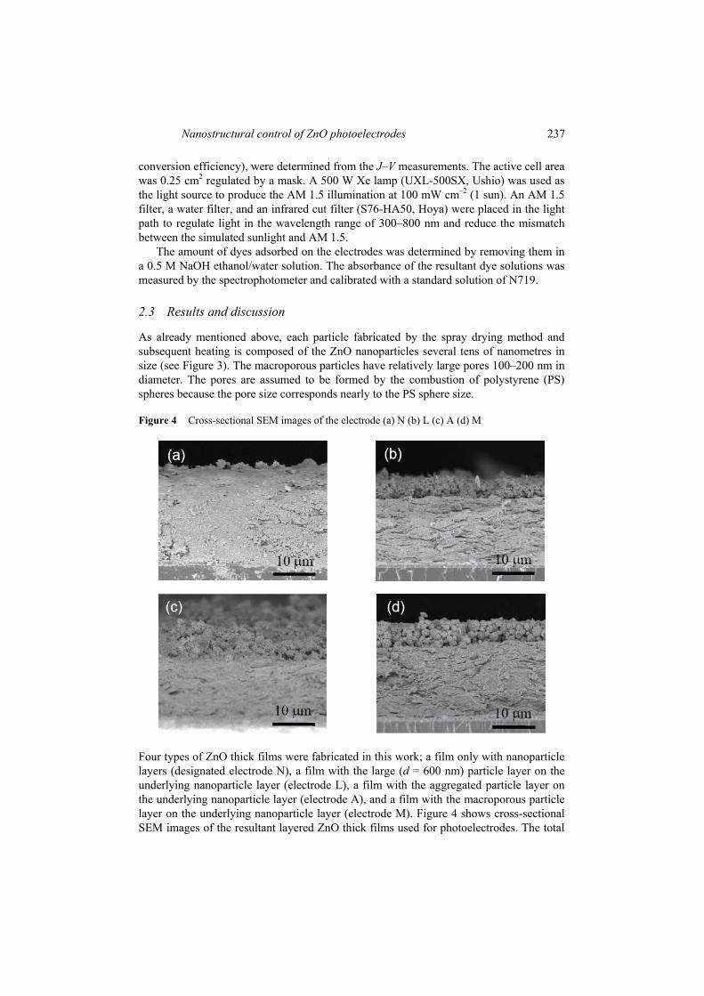
To evaluate the effect of the light scattering layers, optical transmission spectra of the films were measured and compared. The spectsra were recorded for the ZnO films after dye-loading and results are shown in Figure 5. In the UV region, transmittance of all the ZnO films is approximately 0%, which indicates that the UV light can be scattered and/or absorbed by ZnO and N719 dye. In the visible light region (especially above 550 nm), transmittance of the electrodes having the light scattering layer (L, A, and M) is lower than that of the electrode N without the scattering layer. As ZnO does not absorb the visible light, the lower transmittance in the longer wavelength region is due to light scattering, which leads expectedly to the subsequent absorption by the N719 dye. Among the three types of the scattering layers, the large ZnO particle layer (electrode L) appears to be the most suitable one to scatter the incident sunlight.
Figure 5 Optical transmission spectra of the dye-loaded ZnO electrodes
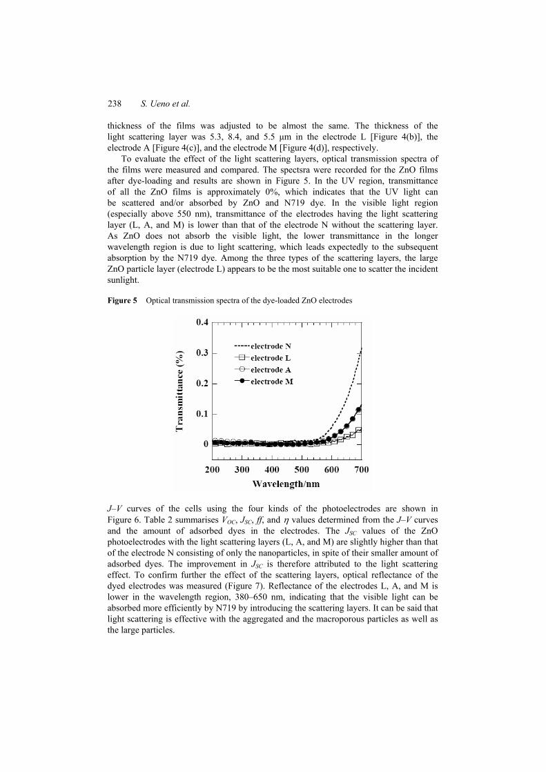
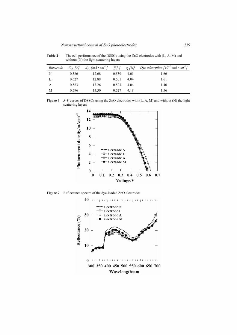
J–V curves of the cells using the four kinds of the photoelectrodes are shown in Figure 6. Table 2 summarises VOC, JSC, ff, and η values determined from the J–V curves and the amount of adsorbed dyes in the electrodes. The JSC values of the ZnO photoelectrodes with the light scattering layers (L, A, and M) are slightly higher than that of the electrode N consisting of only the nanoparticles, in spite of their smaller amount of adsorbed dyes. The improvement in JSC is therefore attributed to the light scattering effect. To confirm further the effect of the scattering layers, optical reflectance of the dyed electrodes was measured (Figure 7). Reflectance of the electrodes L, A, and M is lower in the wavelength region, 380–650 nm, indicating that the visible light can be absorbed more efficiently by N719 by introducing the scattering layers. It can be said that light scattering is effective with the aggregated and the macroporous particles as well as the large particles.
Nanostructural control of ZnO photoelectrodes 239
Table 2 The cell performance of the DSSCs using the ZnO electrodes with (L, A, M) and without (N) the light scattering layers
Electrode VOC [V] JSC [mA · cm–2] ff [-] η [%] Dye adsorption [10–7 mol · cm–2]
N 0.586 12.68 0.539 4.01 1.66 L 0.627 12.88 0.501 4.04 1.61 A 0.583 13.26 0.523 4.04 1.40 M 0.596 13.30 0.527 4.18 1.56
Figure 6 J–V curves of DSSCs using the ZnO electrodes with (L, A, M) and without (N) the light scattering layers
Figure 7 Reflectance spectra of the dye-loaded ZnO electrodes
240 S. Ueno et al.
As to the photovoltage, the VOC value of the electrode L (0.627 V) is higher than that of the other electrodes. This is probably because the large ZnO particles can transport the photogenerated electrons more efficiently. That is, because the large particles have the smaller number of grain boundaries and the smaller area of the ZnO/electrolyte interface, the photogenerated electrons can be transported smoothly with decreasing the chance of the recombination. The highest efficiency of 4.18% was obtained by using the macroporous ZnO particles for the light scattering layer among the four electrodes. Both VOC and JSC were improved in the electrode M, as compared to the electrodes N and A. The large pores in the macroporous particles would facilitate the diffusion of the I–/I3
– redox couples in the liquid electrolyte, which could enhance VOC. In a short summary of this section, it was demonstrated that the macroporous particles
were more suitable for the light scattering layer because they had the large pores for the diffusion of the redox couples, the large surface area for the effective dye adsorption, and the large secondary particle diameter for light scattering. Further work is ongoing to regulate the size and shape of the macroporous ZnO particles more uniformly. One of the promising structures of the light scattering layer may be the inverse opal type using the macroporous particles.
3 Effects of silica nanolayers on ZnO photoelectrodes
3.1 Background
In addition to the modification of the electrode structures, composite structures between ZnO and other materials also seem to be effective for improving the cell performance. We describe here the formation of metal oxide nanolayers on ZnO electrodes for enhancing the charge collection efficiency.
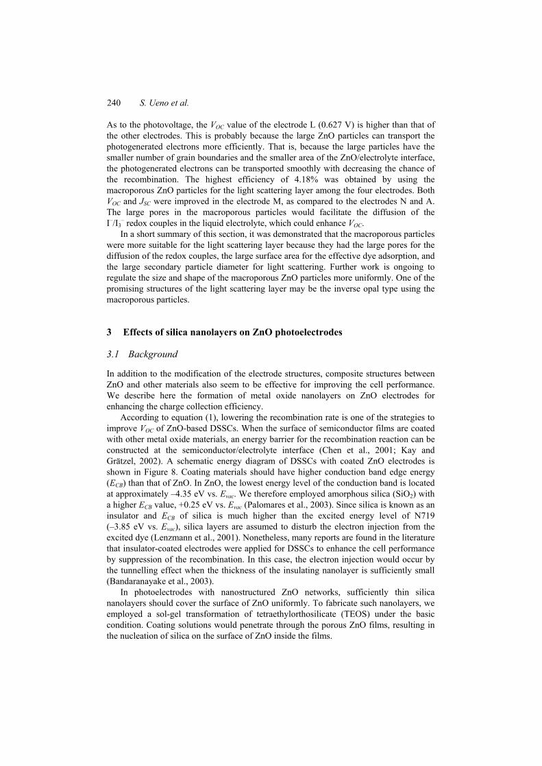
According to equation (1), lowering the recombination rate is one of the strategies to improve VOC of ZnO-based DSSCs. When the surface of semiconductor films are coated with other metal oxide materials, an energy barrier for the recombination reaction can be constructed at the semiconductor/electrolyte interface (Chen et al., 2001; Kay and Grätzel, 2002). A schematic energy diagram of DSSCs with coated ZnO electrodes is shown in Figure 8. Coating materials should have higher conduction band edge energy (ECB) than that of ZnO. In ZnO, the lowest energy level of the conduction band is located at approximately –4.35 eV vs. Evac. We therefore employed amorphous silica (SiO2) with a higher ECB value, +0.25 eV vs. Evac (Palomares et al., 2003). Since silica is known as an insulator and ECB of silica is much higher than the excited energy level of N719 (–3.85 eV vs. Evac), silica layers are assumed to disturb the electron injection from the excited dye (Lenzmann et al., 2001). Nonetheless, many reports are found in the literature that insulator-coated electrodes were applied for DSSCs to enhance the cell performance by suppression of the recombination. In this case, the electron injection would occur by the tunnelling effect when the thickness of the insulating nanolayer is sufficiently small (Bandaranayake et al., 2003).
In photoelectrodes with nanostructured ZnO networks, sufficiently thin silica nanolayers should cover the surface of ZnO uniformly. To fabricate such nanolayers, we employed a sol-gel transformation of tetraethylorthosilicate (TEOS) under the basic condition. Coating solutions would penetrate through the porous ZnO films, resulting in the nucleation of silica on the surface of ZnO inside the films.
Nanostructural control of ZnO photoelectrodes 241
Figure 8 A schematic of the suppression of the recombination by constructing an energy barrier at the ZnO/electrolyte interface (see online version for colours)
3.2 Experimental
Porous ZnO films were fabricated first by a chemical bath deposition (CBD) method which was reported in detail elsewhere (Hosono et al., 2004b; Kakiuchi et al., 2006). Zinc acetate dihydrate (Zn(CH3COO)2·2H2O, Wako Pure Chemical Industries Co., Ltd., Japan) was dissolved in dehydrate methanol with a concentration of 0.15 M. FTO substrates were immersed in this solution and kept at 60ºC for 30 h in a dry bath. Films of layered hydroxide zinc acetate (LHZA) were deposited on both sides of the substrates. Unnecessary films on the bottom side (opposite to the FTO coated side) were scratched off. The LHZA films were then heated at 450ºC for 10 min, followed by quenching. Porous ZnO films with a flowerlike morphology were thus obtained on the FTO substrates. The films consisted of ZnO nanocrystals approximately 20 nm in diameter and had large voids as well as nanopores. This kind of porous structure is expected to facilitate the diffusion of a solution for the nanolayer coating.
Coating solutions were prepared from 40 μL of TEOS (Wako), 500 μL of aqueous ammonia solution (28% mass/mass, Wako), and 20 ml of ion exchange water. They were mixed by ultrasonicating and stirring simultaneously. Coating was carried out using a dip-coating technique. The ZnO films were immersed in the coating solutions and withdrawn with a speed of 0.1 mm/s using a micro speed dip coater (MS215, Asumi Giken Ltd., Japan). The coated films were immediately washed by a mixture of modified ethanol and water. The films were heated at 500ºC or 600ºC for 10 min in air. The coated ZnO films were immersed in the N719 ethanolic solution (0.3 mM) at 60ºC for 30 min. The photoelectrodes fabricated from the coated ZnO films heated at 500ºC and 600ºC are designated S-500 and S-600, respectively. A reference ZnO electrode was also fabricated by the same way without the silica coating and the following heating.
The structure of silica nanolayers was examined by transmission electron microscopy (TEM, Tecnai Spirits, FEI) and X-ray photoelectron spectroscopy (XPS, JPS 9000MX, JEOL). The other analysis methods were the same as described in 2.2.
242 S. Ueno et al.
The cell performance using the S-500 and the S-600 electrode was measured in the same way as described in 2.2. Additionally, dark current-voltage curves were also measured under the dark condition.
3.3 Results and discussion
We have reported recently that a core-shell type coating on ZnO particles is possible by the sol-gel transformation of TEOS. In that case, structures of silica layers formed on each ZnO particle, such as the thickness and surface coverage, depended on the concentration of TEOS and the coating time. By using the dip-coating method, thin silica nanolayers could be formed on the ZnO particles (Ueno and Fujihara, 2010b). Basically, the silica nanolayers are formed by the following hydrolysis and condensation reaction,
( ) ( ) ( )2 5 2 5 2 54 4Si OC H OH Si OC H O C H OHn nn n− −
−+ → + (3)
Si OH O Si Si O Si OH− −≡ − + − ≡→≡ − − ≡ (4)
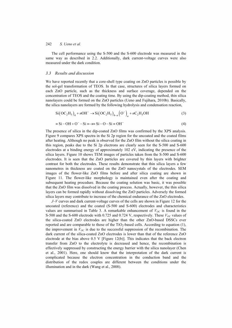
The presence of silica in the dip-coated ZnO films was confirmed by the XPS analysis. Figure 9 compares XPS spectra in the Si 2p region for the uncoated and the coated films after heating. Although no peak is observed for the ZnO film without the silica coating in this region, peaks due to the Si 2p electrons are clearly seen for the S-500 and S-600 electrodes at a binding energy of approximately 102 eV, indicating the presence of the silica layers. Figure 10 shows TEM images of particles taken from the S-500 and S-600 electrodes. It is seen that the ZnO particles are covered by thin layers with brighter contrast for both the electrodes. These results demonstrate that thin silica layers a few nanometres in thickness are coated on the ZnO nanocystals of the electrodes. SEM images of the flower-like ZnO films before and after silica coating are shown in Figure 11. The flower-like morphology is maintained even after the coating and subsequent heating procedure. Because the coating solution was basic, it was possible that the ZnO film was dissolved in the coating process. Actually, however, the thin silica layers can be formed rapidly without dissolving the ZnO particles. Adversely the formed silica layers may contribute to increase of the chemical endurance of the ZnO electrodes.
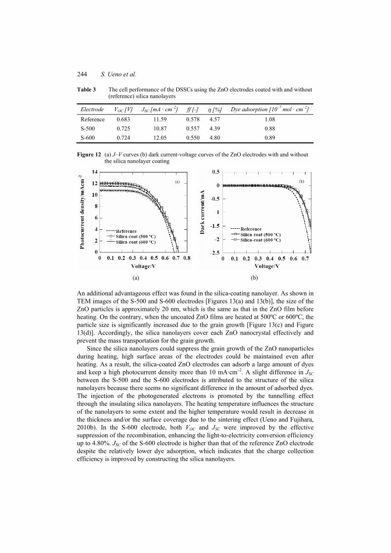
J–V curves and dark current-voltage curves of the cells are shown in Figure 12 for the uncoated (reference) and the coated (S-500 and S-600) electrodes and characteristics values are summarised in Table 3. A remarkable enhancement of VOC is found in the S-500 and the S-600 electrode with 0.725 and 0.724 V, respectively. These VOC values of the silica-coated ZnO electrodes are higher than the other ZnO-based DSSCs ever reported and are comparable to those of the TiO2-based cells. According to equation (1), the improvement in VOC is due to the successful suppression of the recombination. The dark current of the silica-coated ZnO electrodes is lower than that of the reference ZnO electrode at the bias above 0.5 V [Figure 12(b)]. This indicates that the back electron transfer from ZnO to the electrolyte is decreased and hence, the recombination is effectively suppressed by constructing the energy barrier with the silica nanolayer (Chen et al., 2001). Here, one should know that the interpretation of the dark current is complicated because the electron concentration in the conduction band and the distribution of the redox couples are different between the conditions under the illumination and in the dark (Wang et al., 2008).
Nanostructural control of ZnO photoelectrodes 243
Figure 9 XPS spectra of (a) the reference ZnO electrode (b) the S-500 electrode (c) the S-600 electrode in the Si 2p region
Figure 10 TEM images of the particles constructing (a) the S-500 (b) the S-600 electrode
Figure 11 SEM images of (a) the flower-like ZnO films before coating (b) the S-500 (c) the S-600 electrode
(a) (b) (c)
244 S. Ueno et al.
Table 3 The cell performance of the DSSCs using the ZnO electrodes coated with and without (reference) silica nanolayers
Electrode VOC [V] JSC [mA · cm–2] ff [-] η [%] Dye adsorption [10–7 mol · cm–2]
Reference 0.683 11.59 0.578 4.57 1.08 S-500 0.725 10.87 0.557 4.39 0.88 S-600 0.724 12.05 0.550 4.80 0.89
Figure 12 (a) J–V curves (b) dark current-voltage curves of the ZnO electrodes with and without the silica nanolayer coating
(a) (b)
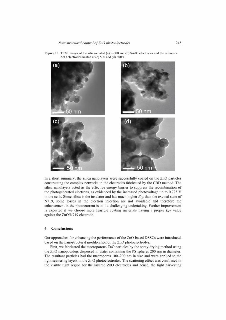
An additional advantageous effect was found in the silica-coating nanolayer. As shown in TEM images of the S-500 and S-600 electrodes [Figures 13(a) and 13(b)], the size of the ZnO particles is approximately 20 nm, which is the same as that in the ZnO film before heating. On the contrary, when the uncoated ZnO films are heated at 500ºC or 600ºC, the particle size is significantly increased due to the grain growth [Figure 13(c) and Figure 13(d)]. Accordingly, the silica nanolayers cover each ZnO nanocrystal effectively and prevent the mass transportation for the grain growth.
Since the silica nanolayers could suppress the grain growth of the ZnO nanoparticles during heating, high surface areas of the electrodes could be maintained even after heating. As a result, the silica-coated ZnO electrodes can adsorb a large amount of dyes and keep a high photocurrent density more than 10 mA·cm–2. A slight difference in JSC between the S-500 and the S-600 electrodes is attributed to the structure of the silica nanolayers because there seems no significant difference in the amount of adsorbed dyes. The injection of the photogenerated electrons is promoted by the tunnelling effect through the insulating silica nanolayers. The heating temperature influences the structure of the nanolayers to some extent and the higher temperature would result in decrease in the thickness and/or the surface coverage due to the sintering effect (Ueno and Fujihara, 2010b). In the S-600 electrode, both VOC and JSC were improved by the effective suppression of the recombination, enhancing the light-to-electricity conversion efficiency up to 4.80%. JSC of the S-600 electrode is higher than that of the reference ZnO electrode despite the relatively lower dye adsorption, which indicates that the charge collection efficiency is improved by constructing the silica nanolayers.
Nanostructural control of ZnO photoelectrodes 245
Figure 13 TEM images of the silica-coated (a) S-500 and (b) S-600 electrodes and the reference ZnO electrodes heated at (c) 500 and (d) 600ºC
In a short summary, the silica nanolayers were successfully coated on the ZnO particles constructing the complex networks in the electrodes fabricated by the CBD method. The silica nanolayers acted as the effective energy barrier to suppress the recombination of the photogenerated electrons, as evidenced by the increased photovoltage up to 0.725 V in the cells. Since silica is the insulator and has much higher ECB than the excited state of N719, some losses in the electron injection are not avoidable and therefore the enhancement in the photocurrent is still a challenging undertaking. Further improvement is expected if we choose more feasible coating materials having a proper ECB value against the ZnO/N719 electrode.
4 Conclusions
Our approaches for enhancing the performance of the ZnO-based DSSCs were introduced based on the nanostructural modification of the ZnO photoelectrodes.
First, we fabricated the macroporous ZnO particles by the spray drying method using the ZnO nanopowders dispersed in water containing the PS spheres 200 nm in diameter. The resultant particles had the macropores 100–200 nm in size and were applied to the light scattering layers in the ZnO photoelectrodes. The scattering effect was confirmed in the visible light region for the layered ZnO electrodes and hence, the light harvesting
246 S. Ueno et al.
efficiency was slightly enhanced. Additionally, VOC was slightly improved because the macropores in the ZnO electrode could facilitate the diffusion of the redox couples in the electrolyte. The macroporous particles had the larger surface area than the dense large particles, which was beneficial to load the larger amount of dyes. The energy conversion efficiency was improved up to 4.18% by using the ZnO electrode with the light scattering layer of the macroporous particles.
Second, the silica nanolayers were coated on the ZnO electrodes by the sol-gel transformation to suppress the recombination of the photogenerated electrons and improve the charge collection efficiency. VOC was increased up to 0.725 V in the silica-coated ZnO electrodes. Since the thickness of the coating layers was as small as a few nanometres, they could act as the energy barrier for the recombination at the ZnO/electrolyte interface. Moreover, the silica nanolayers were found to retard the mass transportation for the grain growth of ZnO. As a result, the silica-coated ZnO photoelectrodes were capable of loading the large amount of dyes and keeping the higher photocurrent. Both VOC and JSC were improved in the silica-coated ZnO electrodes and the energy conversion efficiency was increased up to 4.80%.
The experimental results shown in this article demonstrate that ZnO is the promising alternative material to TiO2 as photoelectrodes of DSSCs by making appropriate modifications of nanostructures. It is the materials scientists who are familiar with the processing of materials from a nanometre to a micrometer scale. We believe that the sense of materials processing is the key to achieving more excellent photoanodes with higher performance.
References Bandaranayake, P.K.M., Jayaweera, P.V.V. and Tennakone, K. (2003) ‘Dye-sensitization of
magnesium-oxide-coated cadmium sulfide’, Solar Energy Materials & Solar Cells, Vol. 76, p.57.
Bauer, C., Boschloo, G., Mukhtar, E. and Hagfeldt, A. (2001) ‘Electron injection and recombination in Ru(dcbpy)(NCS) sensitized nanostructured ZnO’, The Journal of Physical Chemistry B, Vol. 105, p.5585.
Chen, S.G., Chappel, S., Diamant, Y. and Zaban, A. (2001) ‘Preparation of Nb2O5 coated TiO2 nanoporous electrodes and their application in dye-sensitized solar cells’, Chemistry of Materials, Vol. 13, p.4629.
Chou, T.P., Zhang, Q. and Cao, G. (2007) ‘Effects of dye loading conditions on the energy conversion efficiency of ZnO and TiO2 dye-sensitized solar cells’, The Journal of Physical Chemistry C, Vol. 111, p.18804.
Grätzel, M. (2001) ‘Photoelectrochemical cells’, Nature, Vol. 414, p.338. Grätzel, M. (2005) ‘Solar energy conversion by dye-sensitized photovoltaic cells’, Inorganic
Chemistry, Vol. 44, p.6841. Hagfeldt, A. and Grätzel, M. (1995) ‘Light-induced redox reactions in nanocrystalline systems’,
Chemical Reviews, Vol. 95, p.49. Hara, K., Horiguchi, T., Kinoshita, T., Sayama, K., Sugihara, H. and Arakawa, H. (2000) ‘Highly
efficient photon-to-electron conversion with mercurochrome-sensitized nanoporous oxide semiconductor solar cells’, Solar Energy Materials & Solar Cells, Vol. 64, p.115.
Hitachi, N. and Fujihara, S. (2010) ‘Advantageous effect of macroporous TiO2 particles on dye-sensitized solar cells’, Key Engineering Materials, Vol. 445, p.78.
Nanostructural control of ZnO photoelectrodes 247
Hosono, E., Fujihara, S. and Kimura, T. (2004a) ‘Synthesis, structure and photoelectrochemical performance of micro/nano-textured ZnO/eosin Y electrodes’, Electrochimica Acta, Vol. 49, p.2287.
Hosono, E., Fujihara, S., Kimura, T. and Imai, H. (2004b) ‘Growth of layered basic zinc acetate in methanolic solutions and its pyrolytic transformation into porous zinc oxide films’, Journal of Colloid and Interface Science, Vol. 272, p.391.
Hosono, E., Fujihara, S., Honma, I. and Zhou, H. (2005) ‘The fabrication of an upright-standing zinc oxide nanosheet for use in dye-sensitized solar cells’, Advanced Materials, Vol. 17, p.2091.
Iskandar, F., Nandiyanto, A.B.D., Yun, K.M., Hogan, C.J. and Okuyama, K. (2007) ‘Enhanced photocatalytic performance of brookite TiO2 macroporous particles prepared by spray drying with colloidal templating’, Advanced Materials, Vol. 19, p.1408.
Jose, R., Thavasi, V. and Ramakrishna, S. (2009) ‘Metal oxides for dye-sensitized solar cells’, Journal of the American Ceramic Society, Vol. 92, p.289.
Kakiuchi, K., Hosono, E. and Fujihara, S. (2006) ‘Enhanced photoelectrochemical performance of ZnO electrodes sensitized with N-719’, Journal of Photochemistry and Photobiology A: Chemistry, Vol. 179, p.81.
Kakiuchi, K., Saito, M. and Fujihara, S. (2008) ‘Fabrication of ZnO films consisting of densely accumulated mesoporous nanosheets and their dye-sensitized solar cell performance’, Thin Solid Films, Vol. 516, p.2026.
Kay, A. and Grätzel, M. (2002) ‘Dye-sensitized core-shell nanocrystals: improved efficiency of mesoporous tin oxide electrodes coated with a thin layer of an insulating oxide’, Chemistry of Materials, Vol. 14, p.2930.
Lenzmann, F., Krueger, J., Burnside, S., Brooks, K., Grätzel, M., Gal, D., Rühle, S. and Cahen, D. (2001) ‘Surface photovoltage spectroscopy of dye-sensitized solar cells with TiO2, Nb2O5, and SrTiO3 nanocrystalline photoanodes: indication for electron injection from higher excited dye states’, The Journal of Physical Chemistry B, Vol. 105, p.6347.
O’Regan, B. and Grätzel, M. (1991) ‘A low-cost, high-efficiency solar cell based on dye-sensitized colloidal TiO2 films’, Nature, Vol. 353, p.737.
Palomares, E., Clifford, J.N., Haque, S.A., Lutz, T. and Durrant. J.R. (2003) ‘Control of charge recombination dynamics in dye sensitized solar cells by the use of conformally deposited metal oxide blocking layers’, Journal of the American Chemical Society, Vol. 125, p.475.
Saito, M. and Fujihara, S. (2008) ‘Large photocurrent generation in dye-sensitized ZnO solar cells’, Energy & Environmental Science, Vol. 1, p.280.
Saito, M. and Fujihara, S. (2009) ‘Fabrication and photovoltaic properties of dye-sensitized ZnO thick films by a facile doctor-blade printing method using nanocrystalline pastes’, Journal of the Ceramic Society of Japan, Vol. 117, p.823.
Sayama, K., Sugihara, H. and Arakawa, H. (1998) ‘Photoelectrochemical properties of a porous Nb2O5 electrode sensitized by a ruthenium dye’, Chemistry of Materials, Vol. 10, p.3825.
Ueno, S. and Fujihara, S. (2010a) ‘Influence of sintering behavior of ZnO nanoparticles on J–V characteristics of ZnO-based dye-sensitized solar cells’, Key Engineering Materials, Vol. 445, p.117.
Ueno, S. and Fujihara, S. (2010b) ‘Formation of silica nanolayers on ZnO electrodes in dye-sensitized solar cells’, European Journal of Inorganic Chemistry, Vol. 2010, p.2165.
Wang, Q., Zhang, Z., Zakeeruddin, S.M. and Grätzel, M. (2008) ‘Enhancement of the performance of dye-sensitized solar cell by formation of shallow transport levels under visible light illumination’, The Journal of Physical Chemistry C, Vol. 112, p.7084.
Wang, Z.S., Kawauchi, H., Kashima, T. and Arakawa, H. (2004) ‘Significant influence of TiO2 photoelectrode morphology on the energy conversion efficiency of N719 dye-sensitized solar cell’, Coordination Chemistry Reviews, Vol. 248, p.1381.