igb03n120h2 rev2 4g - infineon technologies
TRANSCRIPT
IGB03N120H2
Power Semiconductors 1 Rev. 2.4 Oct. 07
HighSpeed 2-Technology
• Designed for frequency inverters for washing
machines, fans, pumps and vacuum cleaners • 2nd generation HighSpeed-Technology
for 1200V applications offers: - loss reduction in resonant circuits - temperature stable behavior - parallel switching capability - tight parameter distribution - Eoff optimized for IC =3A
• Qualified according to JEDEC2 for target applications • Pb-free lead plating; RoHS compliant
• Complete product spectrum and PSpice Models : http://www.infineon.com/igbt/ Type VCE IC Eoff Tj Marking Package
IGB03N120H2 1200V 3A 0.15mJ 150°C G03H1202 PG-TO263-3-2
Maximum Ratings
Parameter Symbol Value Unit
Collector-emitter voltage VC E 1200 V Triangular collector current TC = 25°C, f = 140kHz TC = 100°C, f = 140kHz
IC 9.6 3.9
Pulsed collector current, tp limited by Tjmax IC p u l s 9.9 Turn off safe operating area VCE ≤ 1200V, Tj ≤ 150°C
- 9.9
A
Gate-emitter voltage VG E ±20 V
Power dissipation TC = 25°C
P t o t 62.5 W
Operating junction and storage temperature T j , T s t g -40...+150 Soldering temperature (reflow soldering, MSL1) - 245
°C
2 J-STD-020 and JESD-022
G
C
E
PG-TO263-3-2
IGB03N120H2
Power Semiconductors 2 Rev. 2.4 Oct. 07
Thermal Resistance
Parameter Symbol Conditions Max. Value Unit
Characteristic IGBT thermal resistance, junction – case
R t h J C 2.0
Thermal resistance, junction – ambient1)
R t h J A 40
K/W
Electrical Characteristic, at Tj = 25 °C, unless otherwise specified
Value Parameter Symbol Conditions
min. Typ. max. Unit
Static Characteristic Collector-emitter breakdown voltage V ( B R ) C E S VG E=0V, IC=300µA 1200 - -
Collector-emitter saturation voltage VC E ( s a t ) VG E = 15V, IC=3A T j=25°C T j=150°C VG E = 10V, IC=3A, T j=25°C
- - -
2.2 2.5
2.4
2.8 - -
Gate-emitter threshold voltage VG E ( t h ) IC=90µA,VC E=VG E 2.1 3 3.9
V
Zero gate voltage collector current
IC E S VC E=1200V,VG E=0V T j=25°C T j=150°C
- -
- -
20 80
µA
Gate-emitter leakage current IG E S VC E=0V,VG E=20V - - 100 nA Transconductance g f s VC E=20V, IC=3A - 2 - S Dynamic Characteristic Input capacitance C i s s - 205 - Output capacitance Co s s - 24 - Reverse transfer capacitance C r s s
VC E=25V, VG E=0V, f=1MHz - 7 -
pF
Gate charge QG a t e VC C=960V, IC=3A VG E=15V
- 22 - nC
Internal emitter inductance measured 5mm (0.197 in.) from case
LE -
7 -
nH
1) Device on 50mm*50mm*1.5mm epoxy PCB FR4 with 6cm2 (one layer, 70µm thick) copper area for collector connection. PCB is vertical without blown air.

IGB03N120H2
Power Semiconductors 3 Rev. 2.4 Oct. 07
Switching Characteristic, Inductive Load, at Tj=25 °C Value
Parameter Symbol Conditions min. typ. max.
Unit
IGBT Characteristic Turn-on delay time td ( o n ) - 9.2 - Rise time t r - 5.2 - Turn-off delay time td ( o f f ) - 281 - Fall time t f - 29 -
ns
Turn-on energy Eo n - 0.14 - Turn-off energy Eo f f - 0.15 - Total switching energy E t s
T j=25°C, VC C=800V, IC=3A, VG E=15V/0V, RG=82Ω , Lσ
2 )=180nH, Cσ
2 )=40pF Energy losses include “tail” and diode 4) reverse recovery.
- 0.29 -
mJ
Switching Characteristic, Inductive Load, at Tj=150 °C
Value Parameter Symbol Conditions
min. typ. max. Unit
IGBT Characteristic Turn-on delay time td ( o n ) - 9.4 - Rise time t r - 6.7 - Turn-off delay time td ( o f f ) - 340 - Fall time t f - 63 -
ns
Turn-on energy Eo n - 0.22 - Turn-off energy Eo f f - 0.26 - Total switching energy E t s
T j=150°C VC C=800V, IC=3A, VG E=15V/0V, RG=82Ω , Lσ
2 )=180nH, Cσ
2 )=40pF Energy losses include “tail” and diode 3)
reverse recovery.
- 0.48 -
mJ
Switching Energy ZVT, Inductive Load
Value Parameter Symbol Conditions
min. typ. max. Unit
IGBT Characteristic Turn-off energy Eo f f VC C=800V,
IC=3A, VG E=15V/0V, RG=82Ω , Cr
2 )=4nF T j=25°C T j=150°C
- -
0.05 0.09
- -
mJ
2) Leakage inductance Lσ and stray capacity Cσ due to dynamic test circuit in figure E 4) Commutation diode from device IKP03N120H2
IGB03N120H2
Power Semiconductors 4 Rev. 2.4 Oct. 07
I C, C
OLL
EC
TOR
CU
RR
EN
T
10Hz 100Hz 1kHz 10kHz 100kHz0A
2A
4A
6A
8A
10A
12A
TC=110°C
TC=80°C
I C, C
OLL
EC
TOR
CU
RR
EN
T
1V 10V 100V 1000V,01A
0,1A
1A
10A
100µs
DC
500µs
10µs
5µs
50µs
tp=1µs
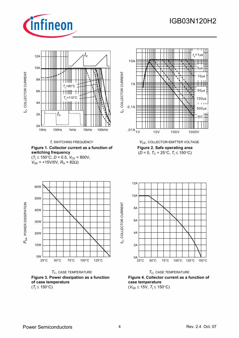
f, SWITCHING FREQUENCY VCE, COLLECTOR-EMITTER VOLTAGE Figure 1. Collector current as a function of switching frequency (Tj ≤ 150°C, D = 0.5, VCE = 800V, VGE = +15V/0V, RG = 82Ω)
Figure 2. Safe operating area (D = 0, TC = 25°C, Tj ≤ 150°C)
P tot, P
OW
ER
DIS
SIPA
TIO
N
25°C 50°C 75°C 100°C 125°C0W
10W
20W
30W
40W
50W
60W
I C, C
OLL
EC
TOR
CU
RR
EN
T
25°C 50°C 75°C 100°C 125°C 150°C0A
2A
4A
6A
8A
10A
12A
TC, CASE TEMPERATURE TC, CASE TEMPERATURE Figure 3. Power dissipation as a function of case temperature (Tj ≤ 150°C)
Figure 4. Collector current as a function of case temperature (VGE ≤ 15V, Tj ≤ 150°C)
Ic
Ic

IGB03N120H2
Power Semiconductors 5 Rev. 2.4 Oct. 07
I C, C
OLL
EC
TOR
CU
RR
EN
T
0V 1V 2V 3V 4V 5V0A
2A
4A
6A
8A
10A
12V10V 8V 6V
VGE=15V
I C, C
OLL
EC
TOR
CU
RR
EN
T
0V 1V 2V 3V 4V 5V0A
1A
2A
3A
4A
5A
6A
7A
8A
9A
10A
12V10V 8V 6V
VGE=15V
VCE, COLLECTOR-EMITTER VOLTAGE VCE, COLLECTOR-EMITTER VOLTAGE Figure 5. Typical output characteristics (Tj = 25°C)
Figure 6. Typical output characteristics (Tj = 150°C)
I C, C
OLL
EC
TOR
CU
RR
EN
T
3V 5V 7V 9V0A
2A
4A
6A
8A
10A
12A
Tj=+150°C
Tj=+25°C
V CE
(sat
), C
OLL
EC
TOR
-EM
ITTE
R S
ATU
RA
TIO
N V
OLT
AG
E
-50°C 0°C 50°C 100°C 150°C0V
1V
2V
3V
IC=6A
IC=3A
IC=1.5A
VGE, GATE-EMITTER VOLTAGE Tj, JUNCTION TEMPERATURE Figure 7. Typical transfer characteristics (VCE = 20V)
Figure 8. Typical collector-emitter saturation voltage as a function of junction temperature (VGE = 15V)
IGB03N120H2
Power Semiconductors 6 Rev. 2.4 Oct. 07
t, S
WIT
CH
ING
TIM
ES
0A 2A 4A1ns
10ns
100ns
1000ns
tr
td(on)
tf
td(off)
t, S
WIT
CH
ING
TIM
ES
0Ω 50Ω 100Ω 150Ω1ns
10ns
100ns
1000ns
tr
td(on)
tf
td(off)
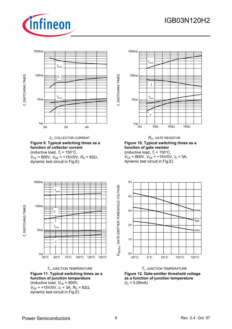
IC, COLLECTOR CURRENT RG, GATE RESISTOR Figure 9. Typical switching times as a function of collector current (inductive load, Tj = 150°C, VCE = 800V, VGE = +15V/0V, RG = 82Ω, dynamic test circuit in Fig.E)
Figure 10. Typical switching times as a function of gate resistor (inductive load, Tj = 150°C, VCE = 800V, VGE = +15V/0V, IC = 3A, dynamic test circuit in Fig.E)
t, S
WIT
CH
ING
TIM
ES
25°C 50°C 75°C 100°C 125°C 150°C1ns
10ns
100ns
1000ns
tr
td(on)
tf
td(off)
V GE
(th),
GA
TE-E
MIT
TER
TH
RE
SHO
LD V
OLT
AG
E
-50°C 0°C 50°C 100°C 150°C0V
1V
2V
3V
4V
5V
typ.
min.
max.
Tj, JUNCTION TEMPERATURE Tj, JUNCTION TEMPERATURE Figure 11. Typical switching times as a function of junction temperature (inductive load, VCE = 800V, VGE = +15V/0V, IC = 3A, RG = 82Ω, dynamic test circuit in Fig.E)
Figure 12. Gate-emitter threshold voltage as a function of junction temperature (IC = 0.09mA)

IGB03N120H2
Power Semiconductors 7 Rev. 2.4 Oct. 07
E, S
WIT
CH
ING
EN
ER
GY
LO
SSE
S
0A 2A 4A0.0mJ
0.5mJ
1.0mJ
Eon1
Eoff
Ets1
E, S
WIT
CH
ING
EN
ER
GY
LO
SSE
S
0Ω 50Ω 100Ω 150Ω 200Ω 250Ω
0.2mJ
0.3mJ
0.4mJ
0.5mJ
0.6mJ
0.7mJ
Eon1
Ets1
Eoff
IC, COLLECTOR CURRENT RG, GATE RESISTOR Figure 13. Typical switching energy losses as a function of collector current (inductive load, Tj = 150°C, VCE = 800V, VGE = +15V/0V, RG = 82Ω, dynamic test circuit in Fig.E )
Figure 14. Typical switching energy losses as a function of gate resistor (inductive load, Tj = 150°C, VCE = 800V, VGE = +15V/0V, IC = 3A, dynamic test circuit in Fig.E )
E, S
WIT
CH
ING
EN
ER
GY
LO
SSE
S
25°C 80°C 125°C 150°C
0.1mJ
0.2mJ
0.3mJ
0.4mJ
0.5mJ
Ets1
Eon1
Eoff
E off,
TUR
N O
FF S
WIT
CH
ING
EN
ERG
Y LO
SS
0V/us 1000V/us 2000V/us 3000V/us0.00mJ
0.04mJ
0.08mJ
0.12mJ
0.16mJ
IC=1A, TJ=150°C
IC=1A, TJ=25°C
IC=3A, TJ=150°C
IC=3A, TJ=25°C
Tj, JUNCTION TEMPERATURE dv/dt, VOLTAGE SLOPE Figure 15. Typical switching energy losses as a function of junction temperature (inductive load, VCE = 800V, VGE = +15V/0V, IC = 3A, RG = 82Ω, dynamic test circuit in Fig.E )
Figure 16. Typical turn off switching energy loss for soft switching (dynamic test circuit in Fig. E)
1) Eon and Ets include losses due to diode recovery.
1) Eon and Ets include losses due to diode recovery.
1) Eon and Ets include losses due to diode recovery.

IGB03N120H2
Power Semiconductors 8 Rev. 2.4 Oct. 07
V GE, G
ATE
-EM
ITTE
R V
OLT
AG
E
1µs 10µs 100µs 1ms 10ms 100ms
10-2K/W
10-1K/W
100K/W
0.01
0.02
0.05
0.1
0.2
single pulse
D=0.5
V GE, G
ATE
-EM
ITTE
R V
OLT
AG
E
0nC 10nC 20nC 30nC0V
5V
10V
15V
20V
UCE=240V
UCE
=960V
QGE, GATE CHARGE QGE, GATE CHARGE Figure 17. Typical gate charge (IC = 3A)
Figure 17. Typical gate charge (IC = 3A)
C, C
AP
AC
ITA
NC
E
0V 10V 20V 30V
10pF
100pF
1nF
Crss
Coss
Ciss
V CE, C
OLL
EC
TOR
-EM
ITTE
R V
OLT
AG
E
0.0 0.2 0.4 0.6 0.8 1.0 1.20V
200V
400V
600V
800V
1000V
0A
1A
2A
3A
I CE C
OLL
EC
TOR
CU
RR
EN
T
VCE, COLLECTOR-EMITTER VOLTAGE tp, PULSE WIDTH Figure 18. Typical capacitance as a function of collector-emitter voltage (VGE = 0V, f = 1MHz)
Figure 20. Typical turn off behavior, hard switching (VGE=15/0V, RG=82Ω, Tj = 150°C, Dynamic test circuit in Figure E)
R , ( K / W ) τ , ( s ) 1.082517 0.000795 0.328671 0.000179 0.588811 0.004631
C1=τ1/R1
R1 R2
C2=τ2/R2
IGB03N120H2
Power Semiconductors 9 Rev. 2.4 Oct. 07
V GE, G
ATE
-EM
ITTE
R V
OLT
AG
E
0.0 0.4 0.8 1.2 1.6 2.0 2.4 2.80V
200V
400V
600V
800V
0A
1A
2A
3A
I CE C
OLL
EC
TOR
CU
RR
EN
T
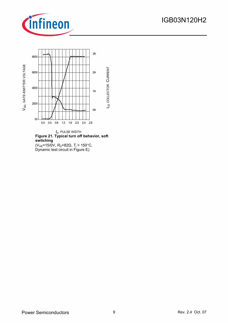
tp, PULSE WIDTH Figure 21. Typical turn off behavior, soft switching (VGE=15/0V, RG=82Ω, Tj = 150°C, Dynamic test circuit in Figure E)

IGB03N120H2
Power Semiconductors 10 Rev. 2.4 Oct. 07
PG-TO263-3-2

IGB03N120H2
Power Semiconductors 11 Rev. 2.4 Oct. 07
Figure A. Definition of switching times
Ir r m
90% Ir r m
10% Ir r m
di /dtF
tr r
IF
i,v
tQS Q
F
tS
tF
VR
di /dtr r
Q =Q Qr r S F
+t =t tr r S F
+
Figure C. Definition of diodes switching characteristics
p(t)1 2 n
T (t)j
τ11
τ22
nn
τ
TC
r r
r
r
rr
Figure D. Thermal equivalent circuit Figure E. Dynamic test circuit Leakage inductance Lσ = 180nH, Stray capacitor Cσ = 40pF, Relief capacitor Cr = 4nF (only for ZVT switching)
Figure B. Definition of switching losses
öö
VDC
DUT(Diode)
½ Lσ
RG DUT(IGBT)
L
½ Lσ
Cσ Cr

IGB03N120H2
Power Semiconductors 12 Rev. 2.4 Oct. 07
Edition 2006-01 Published by Infineon Technologies AG 81726 München, Germany © Infineon Technologies AG 11/6/07. All Rights Reserved. Attention please! The information given in this data sheet shall in no event be regarded as a guarantee of conditions or characteristics (“Beschaffenheitsgarantie”). With respect to any examples or hints given herein, any typical values stated herein and/or any information regarding the application of the device, Infineon Technologies hereby disclaims any and all warranties and liabilities of any kind, including without limitation warranties of non-infringement of intellectual property rights of any third party. Information For further information on technology, delivery terms and conditions and prices please contact your nearest Infineon Technologies Office (www.infineon.com). Warnings Due to technical requirements components may contain dangerous substances. For information on the types in question please contact your nearest Infineon Technologies Office. Infineon Technologies Components may only be used in life-support devices or systems with the express written approval of Infineon Technologies, if a failure of such components can reasonably be expected to cause the failure of that life-support device or system, or to affect the safety or effectiveness of that device or system. Life support devices or systems are intended to be implanted in the human body, or to support and/or maintain and sustain and/or protect human life. If they fail, it is reasonable to assume that the health of the user or other persons may be endangered.