ic fabrication process
TRANSCRIPT

UNIVERSITY OF ENGINEERING AND MANAGEMENT
IC FABRICATION PROCESS
SOUDIP SINHA ROY
ECE .
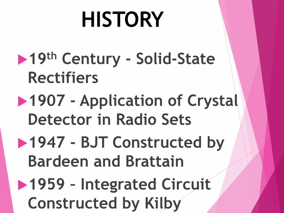
HISTORY
19th Century - Solid-State
Rectifiers
1907 - Application of Crystal
Detector in Radio Sets
1947 - BJT Constructed by
Bardeen and Brattain
1959 – Integrated Circuit
Constructed by Kilby
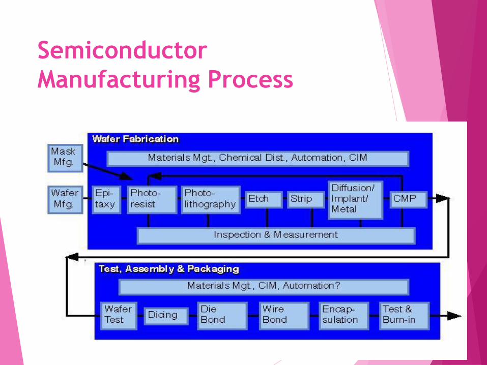
Semiconductor
Manufacturing Process
Semiconductor Manufacturing
Process
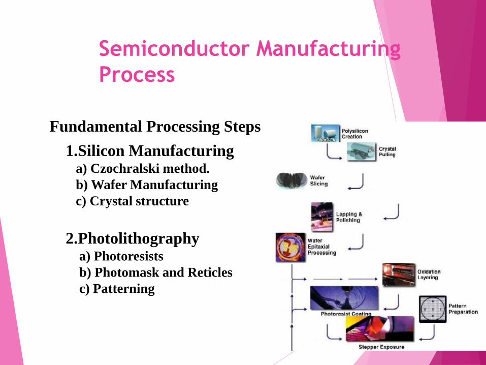
Fundamental Processing Steps
1.Silicon Manufacturinga) Czochralski method.
b) Wafer Manufacturing
c) Crystal structure
2.Photolithographya) Photoresists
b) Photomask and Reticles
c) Patterning
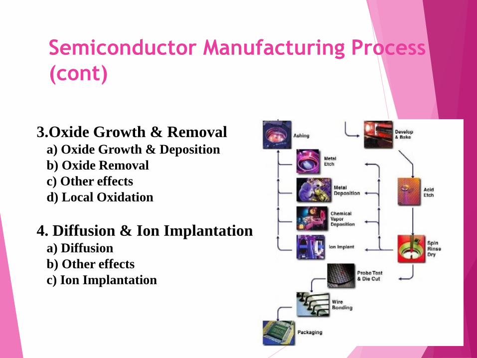
3.Oxide Growth & Removala) Oxide Growth & Deposition
b) Oxide Removal
c) Other effects
d) Local Oxidation
4. Diffusion & Ion Implantationa) Diffusion
b) Other effects
c) Ion Implantation
Semiconductor Manufacturing Process
(cont)
Silicon Manufacturing
Crystal Growth and Wafer Manufacturing
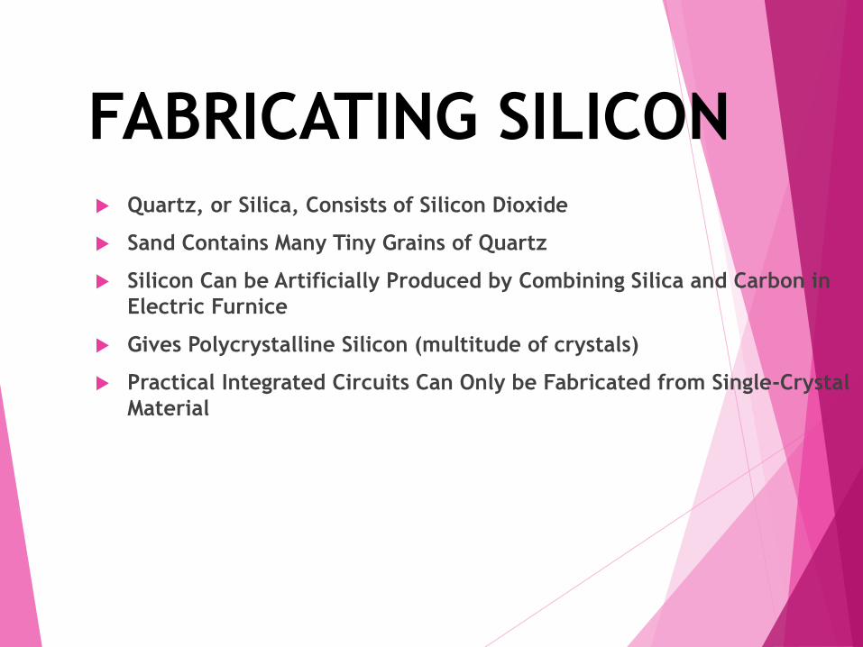
FABRICATING SILICON Quartz, or Silica, Consists of Silicon Dioxide
Sand Contains Many Tiny Grains of Quartz
Silicon Can be Artificially Produced by Combining Silica and Carbon in
Electric Furnice
Gives Polycrystalline Silicon (multitude of crystals)
Practical Integrated Circuits Can Only be Fabricated from Single-Crystal
Material
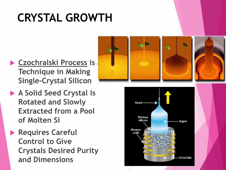
CRYSTAL GROWTH
Czochralski Process is a
Technique in Making
Single-Crystal Silicon
A Solid Seed Crystal is
Rotated and Slowly
Extracted from a Pool
of Molten Si
Requires Careful
Control to Give
Crystals Desired Purity
and Dimensions
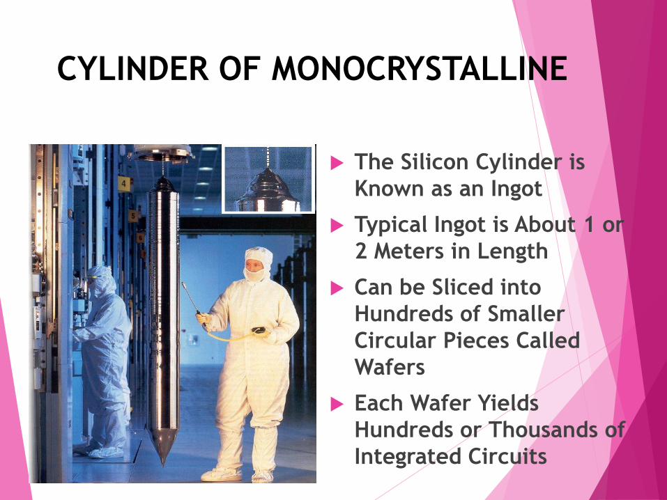
CYLINDER OF MONOCRYSTALLINE
The Silicon Cylinder is
Known as an Ingot
Typical Ingot is About 1 or
2 Meters in Length
Can be Sliced into
Hundreds of Smaller
Circular Pieces Called
Wafers
Each Wafer Yields
Hundreds or Thousands of
Integrated Circuits
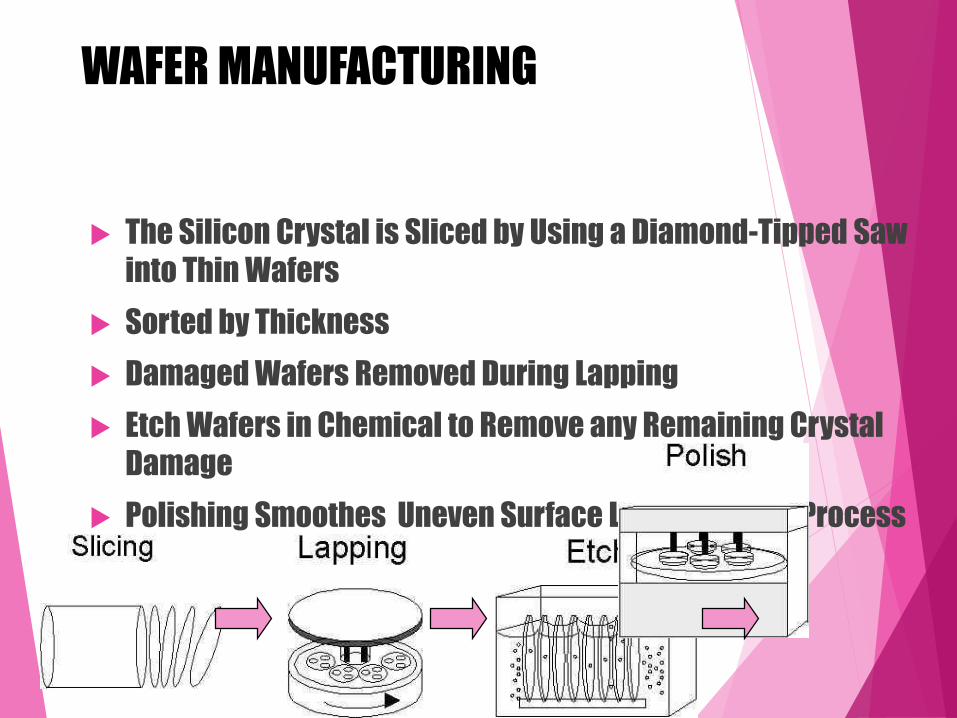
WAFER MANUFACTURING
The Silicon Crystal is Sliced by Using a Diamond-Tipped Saw
into Thin Wafers
Sorted by Thickness
Damaged Wafers Removed During Lapping
Etch Wafers in Chemical to Remove any Remaining Crystal
Damage
Polishing Smoothes Uneven Surface Left by Sawing Process
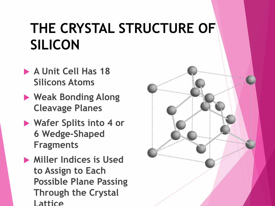
THE CRYSTAL STRUCTURE OF
SILICON
A Unit Cell Has 18
Silicons Atoms
Weak Bonding Along
Cleavage Planes
Wafer Splits into 4 or
6 Wedge-Shaped
Fragments
Miller Indices is Used
to Assign to Each
Possible Plane Passing
Through the Crystal
Lattice
Silicon Manufacturing
Photolithography
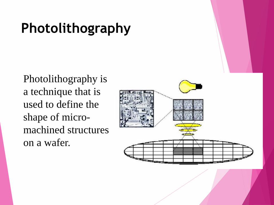
Photolithography
Photolithography is
a technique that is
used to define the
shape of micro-
machined structures
on a wafer.
Photolithography
Photoresist
The first step in the photolithography process is to
develop a mask, which will be typically be a chromium
pattern on a glass plate.
Next, the wafer is then coated with a polymer which is
sensitive to ultraviolet light called a photoresist.
Afterward, the photoresist is then developed which
transfers the pattern on the mask to the photoresist
layer.
Photolithography
Photoresist
There are two basic types of Photoresists Positive and
Negative.
Positive resists.
Positive resists decomposes ultraviolet light. The resist is exposed with UV
light wherever the underlying material is to be removed. In these resists,
exposure to the UV light changes the chemical structure of the resist so
that it becomes more soluble in the developer. The exposed resist is then
washed away by the developer solution, leaving windows of the bare
underlying material. The mask, therefore, contains an exact copy of the
pattern which is to remain on the wafer.
Photolithography
Photoresist
Negative resists
Exposure to the UV light causes the negative resist to become
polymerized, and more difficult to dissolve. Therefore, the negative resist
remains on the surface wherever it is exposed, and the developer solution
removes only the unexposed portions. Masks used for negative
photoresists, therefore, contain the inverse (or photographic "negative")
of the pattern to be transferred.
Photolithography
Model
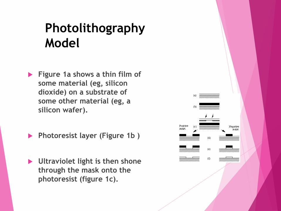
Figure 1a shows a thin film of
some material (eg, silicon
dioxide) on a substrate of
some other material (eg, a
silicon wafer).
Photoresist layer (Figure 1b )
Ultraviolet light is then shone
through the mask onto the
photoresist (figure 1c).
Photolithography
Model
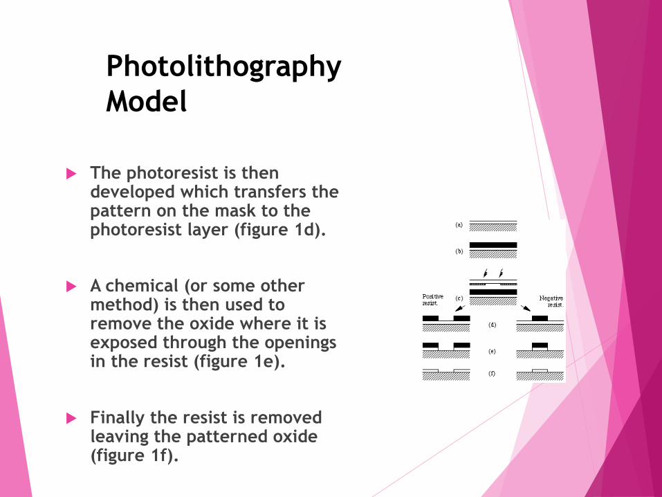
The photoresist is then developed which transfers the pattern on the mask to the photoresist layer (figure 1d).
A chemical (or some other method) is then used to remove the oxide where it is exposed through the openings in the resist (figure 1e).
Finally the resist is removed leaving the patterned oxide (figure 1f).
Photolithography
Photomasks and Reticles
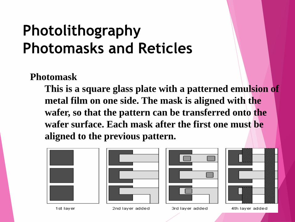
Photomask
This is a square glass plate with a patterned emulsion of
metal film on one side. The mask is aligned with the
wafer, so that the pattern can be transferred onto the
wafer surface. Each mask after the first one must be
aligned to the previous pattern.
Photolithography
Photomasks and Reticles
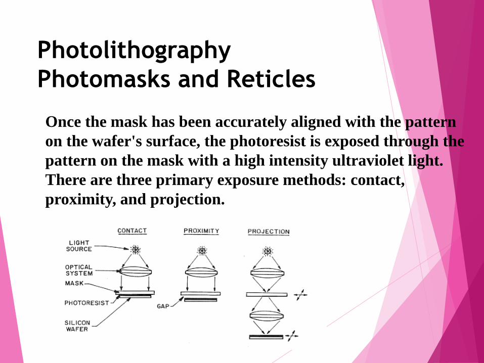
Once the mask has been accurately aligned with the pattern
on the wafer's surface, the photoresist is exposed through the
pattern on the mask with a high intensity ultraviolet light.
There are three primary exposure methods: contact,
proximity, and projection.
Photolithography
Patterning
The last stage of Photolithography is a process called ashing.
This process has the exposed wafers sprayed with a mixture of
organic solvents that dissolves portions of the photoresist .
Conventional methods of ashing require an oxygen-plasma ash,
often in combination with halogen gases, to penetrate the crust
and remove the photoresist. Usually, the plasma ashing process
also requires a follow-up cleaning with wet-chemicals and acids
to remove the residues and non-volatile contaminants that
remain after ashing. Despite this treatment, it is not unusual to
repeat the "ash plus wet-clean" cycle in order to completely
remove all photoresist and residues.
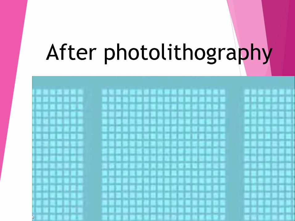
After photolithography

Silicon Manufacturing
Oxidation of Silicon
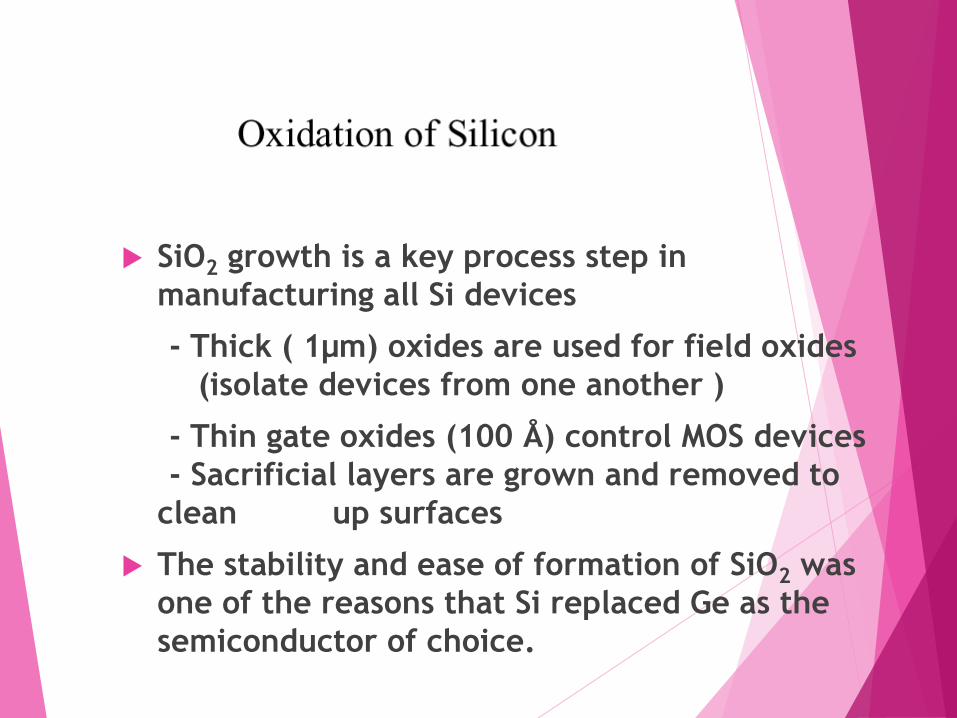
SiO2 growth is a key process step in
manufacturing all Si devices
- Thick ( 1µm) oxides are used for field oxides
(isolate devices from one another )
- Thin gate oxides (100 Å) control MOS devices
- Sacrificial layers are grown and removed to
clean up surfaces
The stability and ease of formation of SiO2 was
one of the reasons that Si replaced Ge as the
semiconductor of choice.
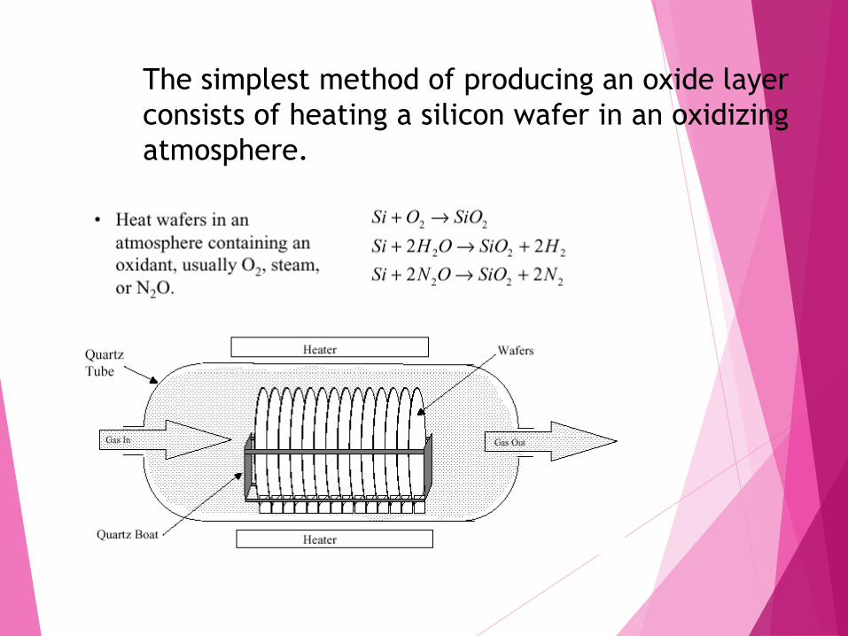
The simplest method of producing an oxide layer
consists of heating a silicon wafer in an oxidizing
atmosphere.
Dry oxide - Pure dry oxygen is employed
Disadvantage
- Dry oxide grows very slowly.
Advantage
- Oxide layers are very uniform.
- Relatively few defects exist at the oxide-silicon
interface (These defects interfere with the proper
operation of semiconductor devices)
- It has especially low surface state charges and thus make ideal dielectrics for MOS transistors.
Wet oxide - In the same way as dry oxides, but
steam is injected
Disadvantage
- Hydrogen atoms liberated by the decomposition of the water molecules produce imperfections that may degrade the oxide quality.
Advantage
- Wet oxide grows fast.
- Useful to grow a thick layer of field oxide
Deposited Oxides
Oxide is frequently employed as an insulator between two layers of metalization. In such cases, some form of deposited oxide must be used rather than the grown oxides.
Deposited oxides can be produced by various reactions between gaseous silicon compounds and gaseous oxidizers. Deposited oxides tend to possess low densities and large numbers of defect sites. Not suitable for use as gate dielectrics for MOS transistors but still acceptable for use as insulating layers between multiple conductor layers, or as protective overcoats.
Key Variables in Oxidation
Temperature
- reaction rate
- solid state diffusion
Oxidizing species
- wet oxidation is much faster than dry oxidation
Surface cleanliness
- metallic contamination can catalyze reaction
- quality of oxide grown (interface states)
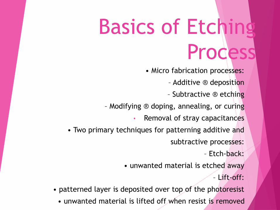
Basics of Etching
Process• Micro fabrication processes:
– Additive ® deposition
– Subtractive ® etching
– Modifying ® doping, annealing, or curing
• Removal of stray capacitances
• Two primary techniques for patterning additive and
subtractive processes:
– Etch-back:
• unwanted material is etched away
– Lift-off:
• patterned layer is deposited over top of the photoresist
• unwanted material is lifted off when resist is removed
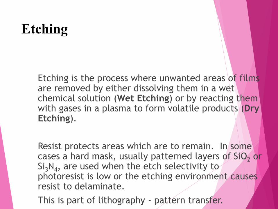
Etching
Etching is the process where unwanted areas of films are removed by either dissolving them in a wet chemical solution (Wet Etching) or by reacting them with gases in a plasma to form volatile products (Dry Etching).
Resist protects areas which are to remain. In some cases a hard mask, usually patterned layers of SiO2 or Si3N4, are used when the etch selectivity to photoresist is low or the etching environment causes resist to delaminate.
This is part of lithography - pattern transfer.
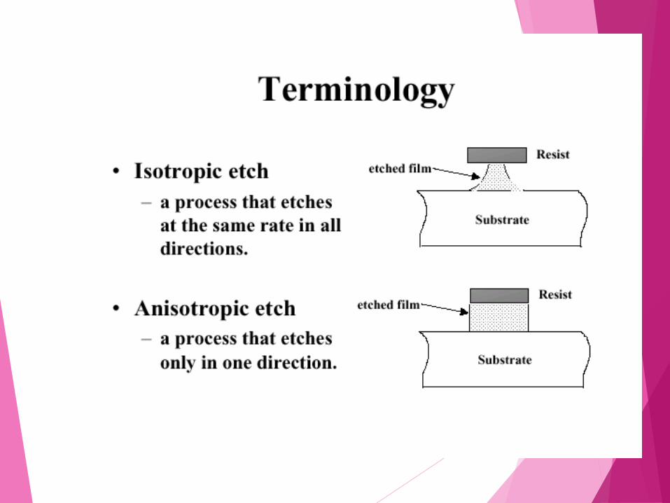
Wet Chemical Etching
Wet etches:
- are in general isotropic
(not used to etch features less than ≈ 3 µm)
- achieve high selectivities for most film
combinations
- capable of high throughputs
- use comparably cheap equipment
- can have resist adhesion problems
- can etch just about anything
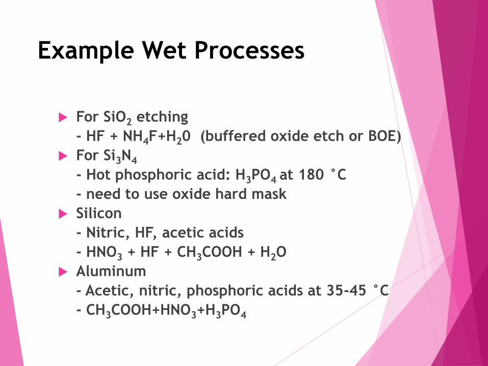
Example Wet Processes
For SiO2 etching
- HF + NH4F+H20 (buffered oxide etch or BOE)
For Si3N4
- Hot phosphoric acid: H3PO4 at 180 °C
- need to use oxide hard mask
Silicon
- Nitric, HF, acetic acids
- HNO3 + HF + CH3COOH + H2O
Aluminum
- Acetic, nitric, phosphoric acids at 35-45 °C
- CH3COOH+HNO3+H3PO4
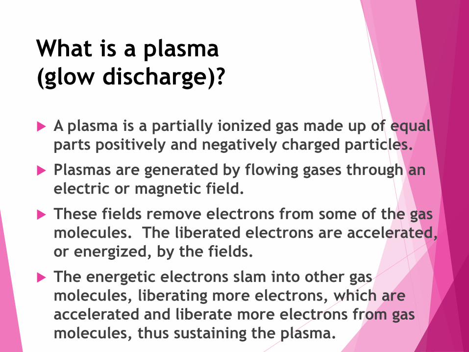
What is a plasma
(glow discharge)?
A plasma is a partially ionized gas made up of equal
parts positively and negatively charged particles.
Plasmas are generated by flowing gases through an
electric or magnetic field.
These fields remove electrons from some of the gas
molecules. The liberated electrons are accelerated,
or energized, by the fields.
The energetic electrons slam into other gas
molecules, liberating more electrons, which are
accelerated and liberate more electrons from gas
molecules, thus sustaining the plasma.
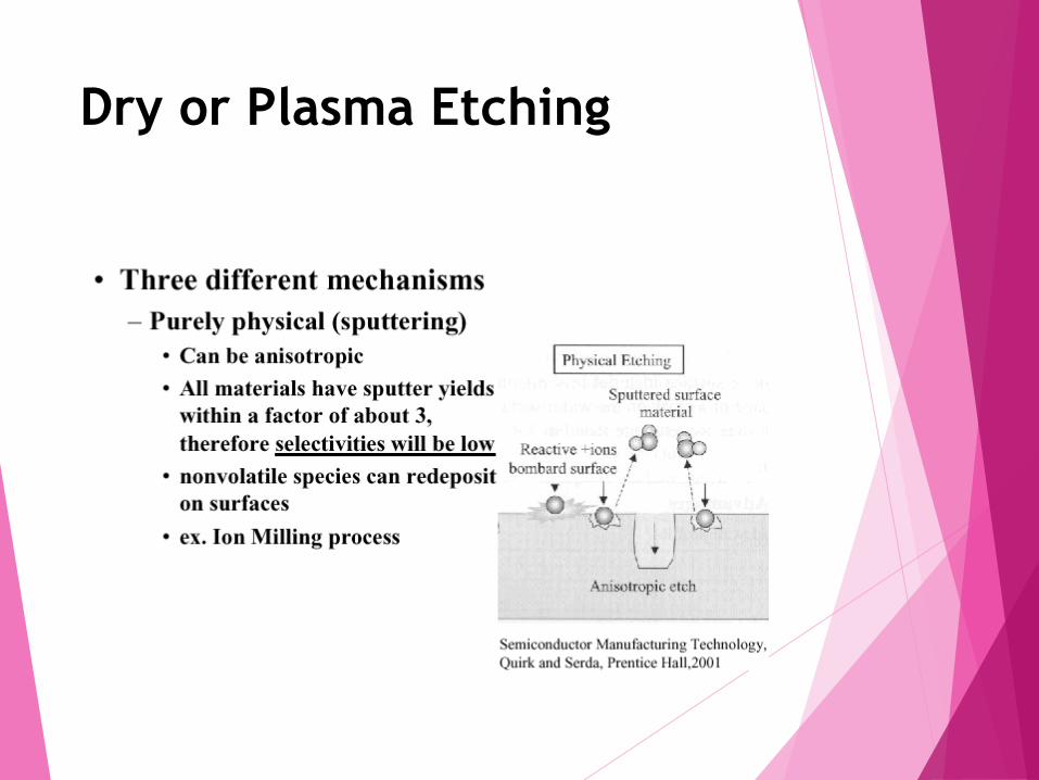
Dry or Plasma Etching
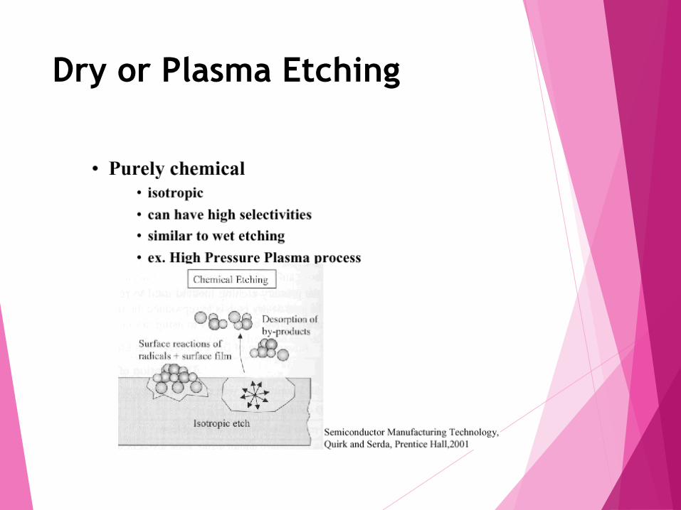
Dry or Plasma Etching
Dry or Plasma Etching
Combination of chemical and physical etching –Reactive Ion Etching (RIE)
Directional etching due to ion assistance.
In RIE processes the wafers sit on the powered electrode. This placement sets up a negative bias on the wafer which accelerates positively charge ions toward the surface. These ions enhance the chemical etching mechanisms and allow anisotropic etching.
Wet etches are simpler, but dry etches provide better line width control since it is anisotropic.
Other Effects of Oxide
Growth and Removal
Oxide Step
- The differences in oxide thickness and in the
depths of the silicon surfaces combine to
produce a characteristic surface discontinuity
The growth of a thermal oxide affects the doping
levels in the underlying silicon
The doping of silicon affects the rate of oxide
growth
Local Oxidation of Silicon
(LOCOS)
LOCOS: localized oxidation of silicon
using silicon nitride as a mask against
thermal oxidation.
A technique called local oxidation of
silicon (LOCOS) allows the selective
growth thick oxide layers
CMOS and BiCMOS processes employ
LOCOS to grow a thick field oxide over
electrically inactive regions of the wafer
Silicon Manufacturing
Diffusion and Ion Implantation
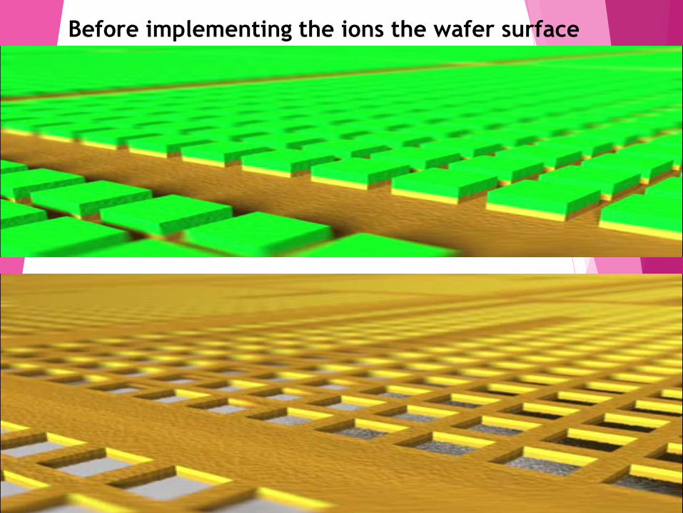
Before implementing the ions the wafer surface
EEEEEE
WN-Junction Fabrication (Earliest
method)
Process:
Opposite polarity doping atoms are added to molten silicon during the Czochralski process to create in-grown junctions in the ingot.
Repeated counterdopings can produce multiple junctions within the crystal.
Disadvantages
Inability to produce differently doped areas in different parts of the wafer.
The thickness and planarity of grown junctions are difficult to control.
Repeated counterdopings degrade the electrical properties of the silicon.
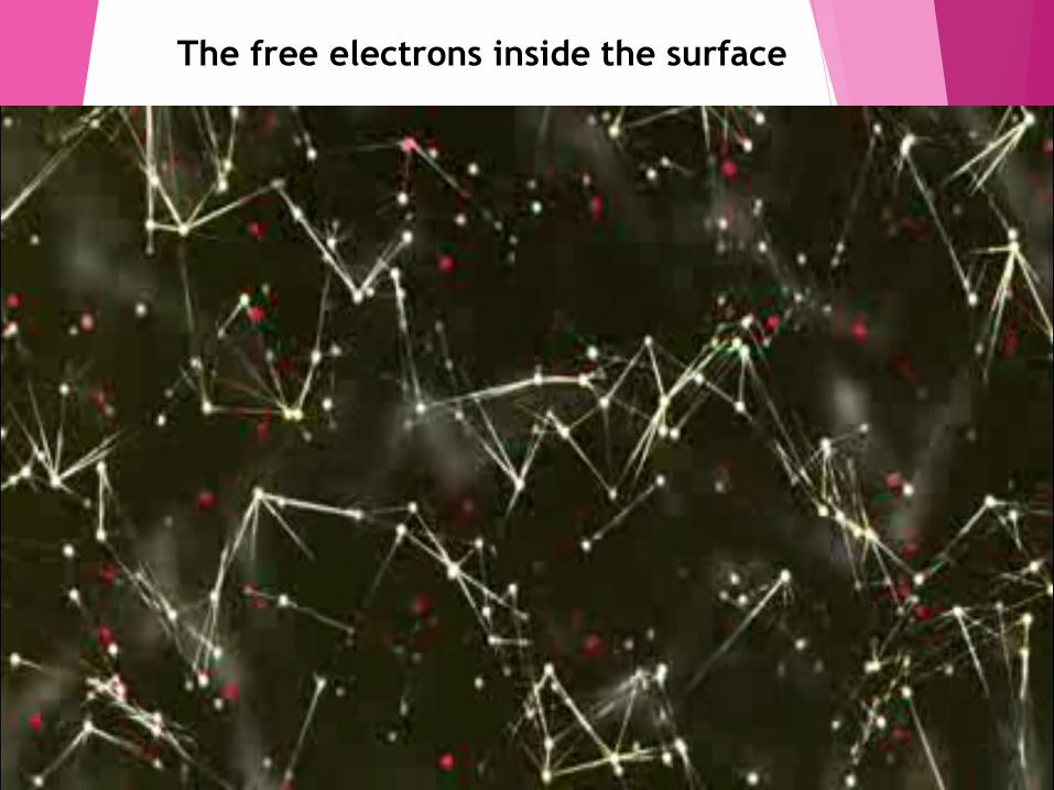
The free electrons inside the surface
The Planar Process
Advantages:
• The planar process does not require multiple
counterdopings of the silicon ingot.
• This process allows more precise control of
junction depths and dopant distributions.
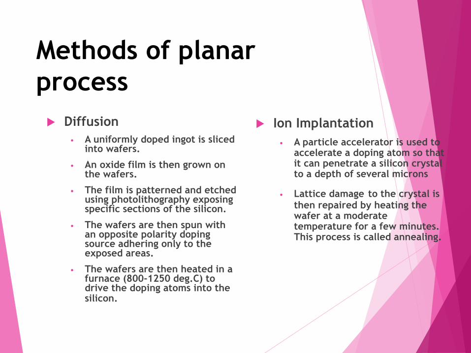
Methods of planar
process
Diffusion
• A uniformly doped ingot is sliced into wafers.
• An oxide film is then grown on the wafers.
• The film is patterned and etched using photolithography exposing specific sections of the silicon.
• The wafers are then spun with an opposite polarity doping source adhering only to the exposed areas.
• The wafers are then heated in a furnace (800-1250 deg.C) to drive the doping atoms into the silicon.
Ion Implantation
• A particle accelerator is used to accelerate a doping atom so that it can penetrate a silicon crystal to a depth of several microns
• Lattice damage to the crystal is then repaired by heating the wafer at a moderate temperature for a few minutes. This process is called annealing.

Diffusion Process Ion
Implantation
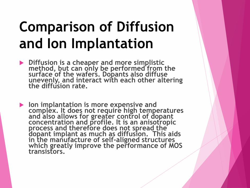
Comparison of Diffusion
and Ion Implantation
Diffusion is a cheaper and more simplistic method, but can only be performed from the surface of the wafers. Dopants also diffuse unevenly, and interact with each other altering the diffusion rate.
Ion implantation is more expensive and complex. It does not require high temperatures and also allows for greater control of dopant concentration and profile. It is an anisotropic process and therefore does not spread the dopant implant as much as diffusion. This aids in the manufacture of self-aligned structures which greatly improve the performance of MOS transistors.

References
www.google.com