i-fuse best otp for fd-soi and...
TRANSCRIPT
11
3rd Annual Tokyo SOI Workshop, May 31th-June 1st, 2017
I-fuseTM:Best OTP for FD-SOI and
Sub-14nm
Shine Chung, Chairman
May, 2017
Attopsemi Technology
1A2-A1 No. 1 Li-Hsin 1st Rd, Hsinchu, Taiwan 300-76
�(886) 3-666-3150x211, (886) 920-566-218
22
3rd Annual Tokyo SOI Workshop, May 31th-June 1st, 2017
About Attopsemi� Founded in June 2010
— By a team of semiconductor veterans and experts
� Located at Si-Soft Research Center of Hsinchu Science Park, Taiwan
� Biz: OTP (One-Time Programmable) IP development and licensing— Foundry independent OTP; no additional masks or process steps
— Program not by NVM ways: blow fuse, rupture oxide or trap charges
— But by “true electromigration: accelerating wear-out of logic devices"
— 100x reliability, 1/100 cell size, and 1/10 program current of eFuse
— Pass HTS at 300oC for 4,290hr; defect rate <0.01ppm
— Universal and proven OTP from 0.7um to 22nm and 7nm and beyond
� Patent portfolio: >65 filed in US and 11 in Taiwan/China
� Engaged >5 foundries and >50 customers worldwide

33
3rd Annual Tokyo SOI Workshop, May 31th-June 1st, 2017
• Founder: Shine Chung• Harvard graduate in Applied Physics• 30 years of IC design experience• Memory design in AMD, Intel, and HP• PA-WW architect (PA-WW: precedent of Intel’s Merced)• Director at TSMC (eFuse pioneer)• VLSI and ISSCC technical committee for 4 years• Two-time TSMC innovation award recipient• More than 61 US patents granted before Attopsemi• Filed more than 65 U.S. patents at Attopsemi Technology
The Team
• Co-founder & VP of Eng: WK Fang• MSEE from Ann Harbor, U. of Michigan• 20-year experiences in memory • Technical Manager at TSMC• Department Mgr for eFuse• Design managers for N90/N65 SRAM TV, eDRAM• MTS in SRAM, FIFO, CAM at IDT
44
3rd Annual Tokyo SOI Workshop, May 31th-June 1st, 2017
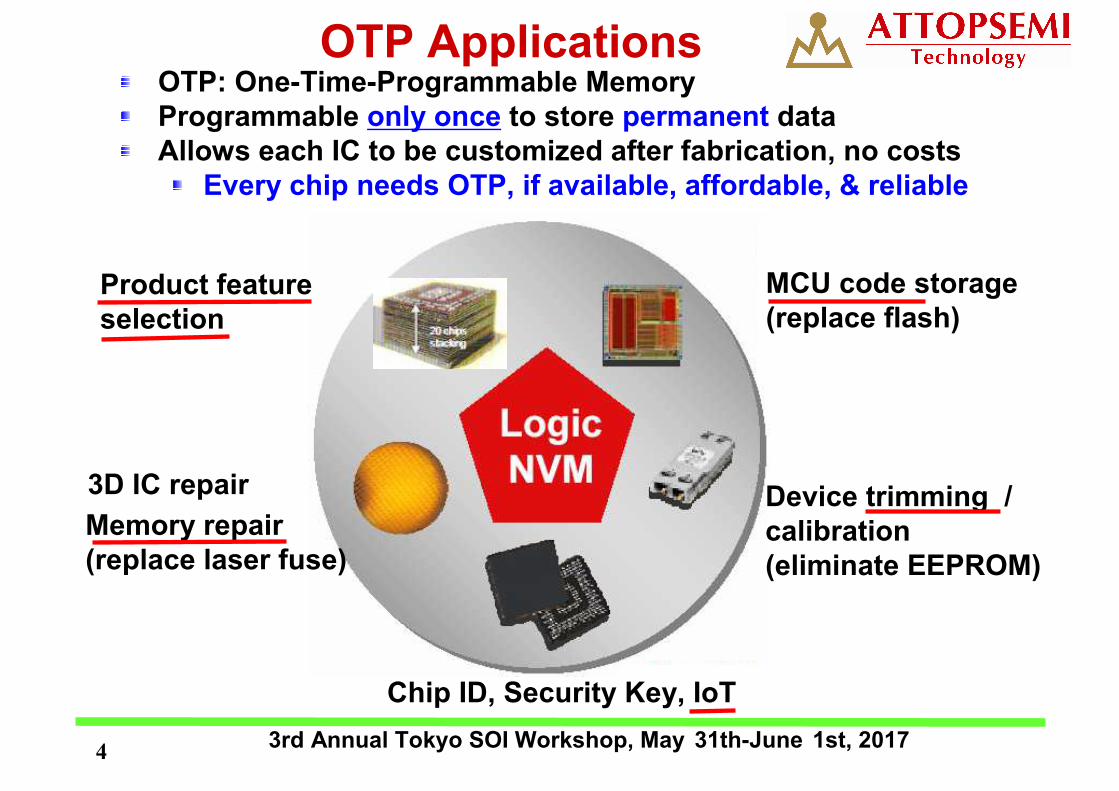
OTP Applications
Memory repair (replace laser fuse)
Chip ID, Security Key, IoT
Device trimming / calibration (eliminate EEPROM)
MCU code storage (replace flash)
Product feature selection
OTP: One-Time-Programmable MemoryProgrammable only once to store permanent dataAllows each IC to be customized after fabrication, no costs
Every chip needs OTP, if available, affordable, & reliable
3D IC repair
55
3rd Annual Tokyo SOI Workshop, May 31th-June 1st, 2017
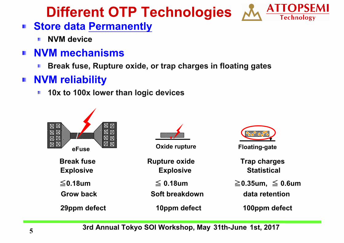
Different OTP TechnologiesStore data Permanently
NVM device
NVM mechanismsBreak fuse, Rupture oxide, or trap charges in floating gates
NVM reliability10x to 100x lower than logic devices
Floating-gateOxide ruptureeFuse
Break fuse Rupture oxide Trap charges
≦0.18um ≦ 0.18um ≧0.35um, ≦ 0.6um
Explosive Explosive Statistical
Grow back Soft breakdown data retention
29ppm defect 10ppm defect 100ppm defect
66
3rd Annual Tokyo SOI Workshop, May 31th-June 1st, 2017
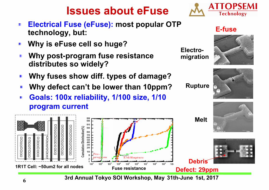
Issues about eFuseElectrical Fuse (eFuse): most popular OTP technology, but:
1R1T Cell: ~50um2 for all nodes
Why is eFuse cell so huge?
Why post-program fuse resistance distributes so widely?
Debris
Fuse resistance
Why fuses show diff. types of damage?
Electro-migration
Rupture
Melt
E-fuse
Why defect can’t be lower than 10ppm?
Defect: 29ppm
Debris
Goals: 100x reliability, 1/100 size, 1/10 program current

77
3rd Annual Tokyo SOI Workshop, May 31th-June 1st, 2017
I-Fuse™: OTP of Choice1R1D(P+/NW diode), NOT 1R1T cell
Diode delivers 5-6x current with 1/5-1/6 of area
=> 1/25-1/36 size of e-fuse from IDMs
=> 1/100 cell size of e-fuse from foundries
1R1D
P+/NW
P+
tap
1R1T
Program current less than Icrit:
Control programming vs. explosion
=>100x reliability; easy to qualified
~100% pgm yield => pre-program fab defects
Defect:<1E-8 (I-fuse); ~1E-6 (e-fuse)
Proprietary fuse to increase program window
IcritI I-fuse E-fuse
•Deterministic
•Multi-shots possible
•Yield: pre-pgm defect
•Defect:<1E-8
•Explosive, chaotic
•One shot only
•Yield: post-pgm reliability
•Defect: ~1E-6
V
1R1D
1R1T
Small fuse and selector
Small size=>heat loss ↓=>pgm eff ↑
And lesser program current than Icrit
=> Need only 1/10 of program current
[email protected](I-fuse) vs. 18mA@N90(e-fuse)
Fuse shape illustrative
purpose

88
3rd Annual Tokyo SOI Workshop, May 31th-June 1st, 2017
What’s I-fuse™ vs eFuse?Breaking fuse: Program beyond a critical current
Explosive programming
=> debirs grow back
Intel: IEDM 1997, pp.855
Any Power Devices would prevent operating under “thermal
run away.” Why a fuse under such condition can be reliable?
IcritII-fuse
V
Attopsemi: ICMTS 2016, pp148
Non-breaking fuse: Program below a critical current Icrit* and above electromigration (EM) threshold*
Deterministic programming
=> ultra-high reliability
Thermal runaway
Electro-migration
threshold
* US patents granted
Breaking fuse: Program beyond a critical current
Explosive programming
=> debris grow back
Intel: IEDM 1997, pp.855Intel: IEDM 1997, pp.855

99
3rd Annual Tokyo SOI Workshop, May 31th-June 1st, 2017
Why Non-breaking Fuse?Many advantages for non-breaking fuses:
=> low program voltage => No charge pump requirement
=> Uses standard logic design/test flow
=> low program current => smaller size
=> lower power
=> control program => tight fuse resistance distribution
=> higher reliability
=> less damage => sustain high temperature
=> higher data security
=> electro-migration => no debris after program =>no grow back
Applications:
Low voltage/current program/read: 0.7um to 14/10/7nm
High quality, reliability: IoT, Automotive, Industry, communication
Only OTP programming mechanism that can be modeled by
physics: heat generation/dissipation and electro-migration

1010
3rd Annual Tokyo SOI Workshop, May 31th-June 1st, 2017
300oC 4Khr I-Fuse™ Bake� We made OTP history: the only OTP passes HTS 300oC, 4,290hr
� 96 dies of 4Kx8 (3Mb I-fuse™) at 0.16um HV pass HTS 300oC, 4Khr
— No defect found and no redundancy
� Cell current variation after stress vs. before stress
— Cell current changes <5% after baking
Cell current before stress
Cell c
urr
en
t aft
er
str
ess
Cell current before & after
Cu
mu
late
d p
erc
en
tag
eProgram bits
Un-program bits

1111
3rd Annual Tokyo SOI Workshop, May 31th-June 1st, 2017
400oC 8hr I-Fuse™ Bake• I-fuse™ cell current variation <5 % after HTS 400oC for 8hrs
– Passing 400oC for >2hr is a must in RDL process for 3D IC
– Foundry eFuse can’t pass 400oC for 2hrs, with 20-30 defects in 1Mb
– 96 4Kx8 I-fuse™ dies @0.16um HV passed @400oC (0 defects in 3Mb)
“0”
“1”
Cell current before burn-in
Cell c
urren
t afte
r b
urn
-in
1212
3rd Annual Tokyo SOI Workshop, May 31th-June 1st, 2017
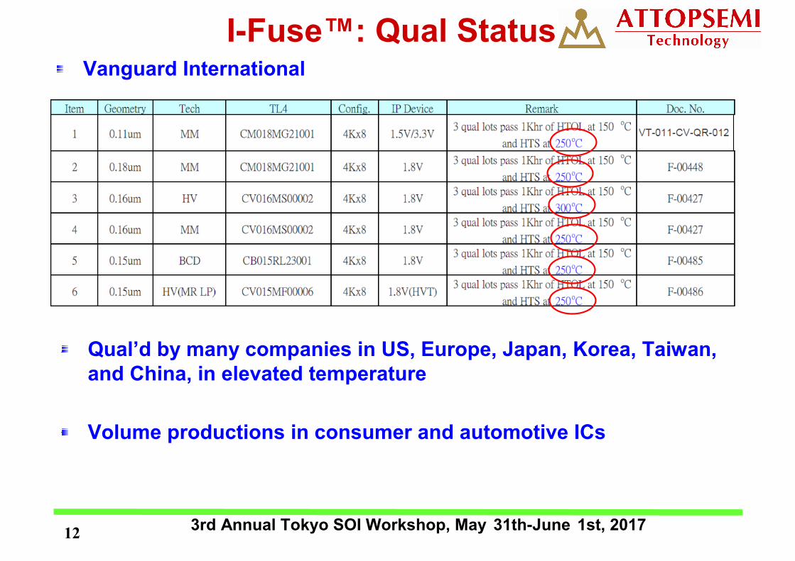
I-Fuse™: Qual Status
Qual’d by many companies in US, Europe, Japan, Korea, Taiwan, and China, in elevated temperature
Volume productions in consumer and automotive ICs
Vanguard International

1313
3rd Annual Tokyo SOI Workshop, May 31th-June 1st, 2017
Why FD-SOI?
Want a phone as small as a watch ?
You need FD-SOI
RF integration (multi-band/mode)
Small form-factor
Ultra-low power (e.g. 0.4V/1uA)
Low costs
2000s 2020s1970s1900s 1950s
1414
3rd Annual Tokyo SOI Workshop, May 31th-June 1st, 2017
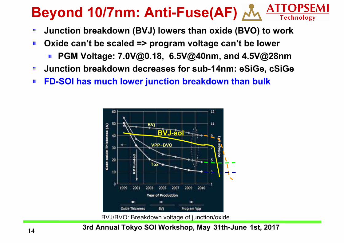
Beyond 10/7nm: Anti-Fuse(AF)
BVJ/BVO: Breakdown voltage of junction/oxide
Junction breakdown (BVJ) lowers than oxide (BVO) to work
Oxide can’t be scaled => program voltage can’t be lower
PGM Voltage: [email protected], 6.5V@40nm, and 4.5V@28nm
Junction breakdown decreases for sub-14nm: eSiGe, cSiGe
FD-SOI has much lower junction breakdown than bulk
VPP~BVO
Tox
BVj
BVJ-soi

1515
3rd Annual Tokyo SOI Workshop, May 31th-June 1st, 2017
Beyond 10/7nm: I-Fuse™I-fuse™ proven from 0.7um to 22nm and soon to 7nm
Programming current scaled with shrinking feature width
So is the program voltage
I-fuse™ @22nm FD-SOI: PGM voltage <1.0V with 1/20 area than AF
Icrit
0
0.002
0.004
0.006
0.008
0.01
0.012
0.014
0.016
0.018
0.02
0.022
0.024
0 50 100 150 200 250 300 350 400 450 500
Lg
For FD-SOI and sub-14nm:
I-fuse™ current programming prevails AF voltage programming !!!

1616
3rd Annual Tokyo SOI Workshop, May 31th-June 1st, 2017
IoT Is Data SecurityWhich I-fuse™ at GF 28nm has been programmed?
Heck a fuse 90% , hack 1Kb ~ 0 (0.91,000=1.39E-47) !!

1717
3rd Annual Tokyo SOI Workshop, May 31th-June 1st, 2017
I-Fuse™: ZERO DefectField return is very costly
10x costs from wafer sort, packaged chip, module, PCB, to system
ZERO defect after shipping
Defects should be found out and screened before shipping
I-fuse™ can achieve ZERO defect
OTP dilemma: fully tested before shipping; can’t be used after tests
Guarantee programmable: if initial fuse resistance <400Ω
Guarantee 100% programmable: if program within specs
Fully testable: every functional block, including program circuits
$0.1 $1 $10 $100 $1000

1818
3rd Annual Tokyo SOI Workshop, May 31th-June 1st, 2017
I-Fuse™ for IoTInternet-of-Things (IoT)
Low cost, low power wireless sensor network30B internet-enabled device by 2020--- 3-5x market of smart phoneFD-SOI is the ideal CMOS technology for IoT
I-fuse™ for IoTLow voltage: I-fuse™ program voltage at 1.0V
Low current: I-fuse™ read voltage at 0.4V, current at 1uA
High data security: I-fuse™ program state undetectable
Sensor ID
Sensor configuration
MCU Code
(OTP)
1919
3rd Annual Tokyo SOI Workshop, May 31th-June 1st, 2017
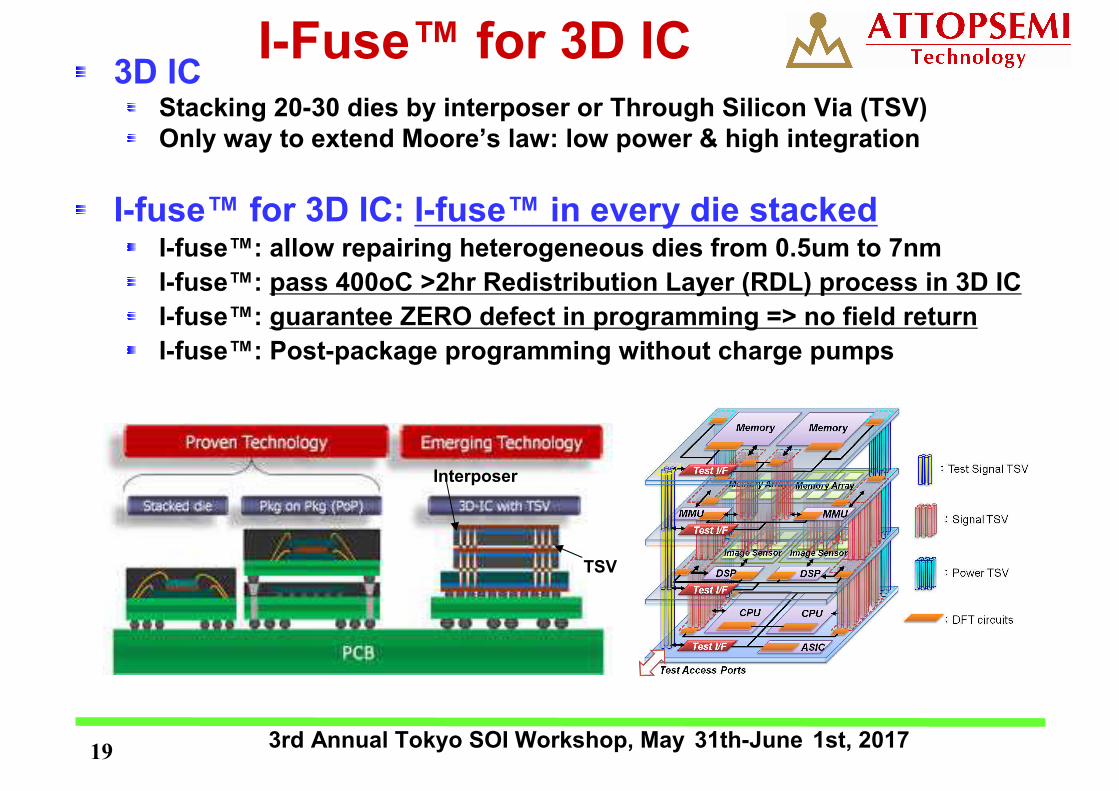
I-Fuse™ for 3D IC3D IC
Stacking 20-30 dies by interposer or Through Silicon Via (TSV)Only way to extend Moore’s law: low power & high integration
I-fuse™ for 3D IC: I-fuse™ in every die stackedI-fuse™: allow repairing heterogeneous dies from 0.5um to 7nm
I-fuse™: pass 400oC >2hr Redistribution Layer (RDL) process in 3D IC
I-fuse™: guarantee ZERO defect in programming => no field return
I-fuse™: Post-package programming without charge pumps
TSV
Interposer

2020
3rd Annual Tokyo SOI Workshop, May 31th-June 1st, 2017
Conclusions• I-fuse™: a proven OTP technology
– Many customers in volume productions
• I-fuse™: the OTP of choice– Scalable: from 0.7um to 7nm and beyond
– Especially for SOI: much lower device breakdown voltage
– High reliability: ZERO defect => guarantee no field return
– High temperature: from -55oC to 200oC
– Small size: up to 1/100 of eFuse, smaller than anti-fuse
– Low program voltage: based on I/O voltages (w/o charge pumps)
– High data security: program status is undetectable
• I-fuse™ enable new OTP applications– IoT: low cost, low power, and high reliability wireless sensor network
– Automotive: qual passed 250oC for 1K hrs
– 3D IC repair: allow heterogeneous dies from diff. foundries repaired
• Call for participation to become industry standard– High quality, high reliability, and save costs

2121
3rd Annual Tokyo SOI Workshop, May 31th-June 1st, 2017
BACKUP

2222
3rd Annual Tokyo SOI Workshop, May 31th-June 1st, 2017
Myths about OTPOTP market size too small
All chips need OTP
1% of royalty for $300B worldwide market means $3B
Majority of OTP in use are in-house eFuse
OTP is an NVM memory and should be qual’d like an NVM
Existing OTPs are NVMs: break fuse, rupture oxide, & trapping charges
Innovative I-fuse(tm) OTP: non-breaking fuse: a logic device
Conventional eFuse programming is based on electromigration (EM)
A mixed of EM/rutpure/decompose/melt under thermal runaway
Breaking a fuse is more reliable
Breaking a fuse by explosion ISN’T; Raising fuse resistance by EM IS
High post- and pre-program fuse resistance ratio is a figure of merit
5X or 10X resistance ratio is good enough for sensing
OTP needs redundancy
OTP should have high yield and high reliability. Needs no redundancy
Floating-gate Oxide rupture I-fuse(tm)eFuse