hybrid modulated bidirectional resonant dc/dc …pearl.shanghaitech.edu.cn/pdf/2019ecce_deng.pdfan...
TRANSCRIPT
Hybrid Modulated Bidirectional Resonant DC/DC Converter for High-Voltage Bus-Based Energy Storage Systems
Junyun Deng, Student Member, IEEE, and Haoyu Wang, Senior Member, IEEE School of Information Science and Technology
ShanghaiTech University, Shanghai, China [email protected]
Abstract—In high-voltage bus-based energy storage systems, an isolated bidirectional dc/dc converter is required to link the low voltage energy storage unit and the high-voltage bus. This paper proposes a series resonant dc/dc converter for this specific application. In the proposed converter, the step-up ratio is boosted by an active voltage quadrupler rectifier on the high voltage side. Thus, a transformer with a moderate turns ratio can be employed. Moreover, the voltage stresses of high voltage side MOSFETs are significantly reduced in comparison with conventional active rectifiers. This facilitates an easier selection of low-cost and highly-reliable Si MOSFETs. To optimize the converter performance, a unique phase-shift and frequency hybrid modulation scheme are proposed. The frequency modulation tightly regulates the output power, while the phase-shit modulation minimizes the conduction loss. A 500 W converter prototype, linking an 80 V-120 V battery pack and 760 V dc bus, is designed and tested to verify the concept.
Keywords—Bidirectional dc/dc converter, phase-shift-modulation (PSM), variable frequency modulation (VFM).
I. INTRODUCTION
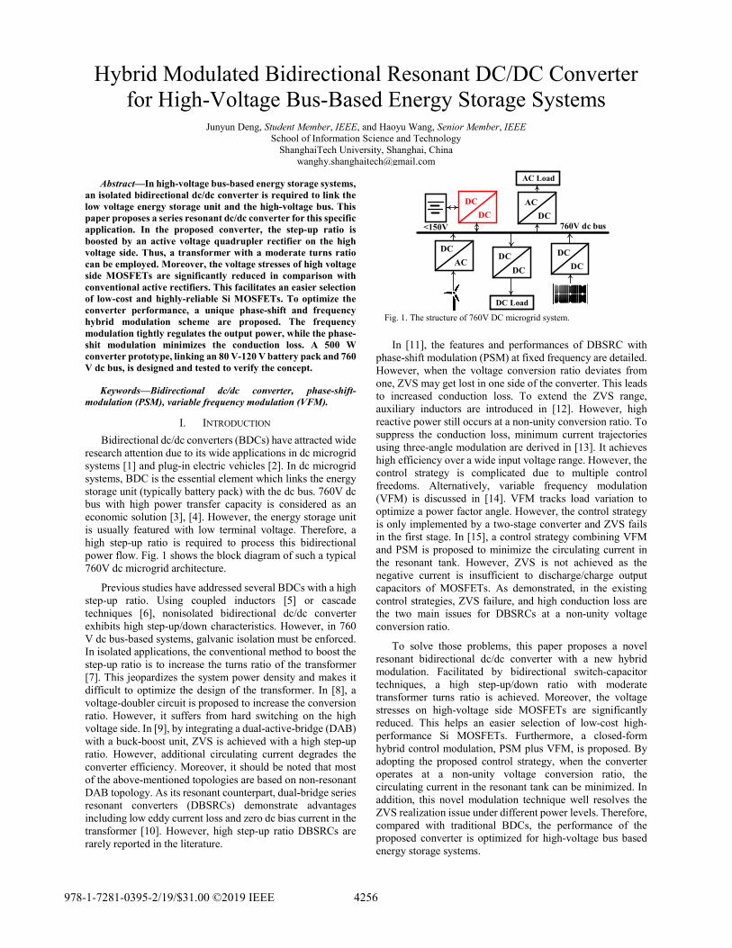
Bidirectional dc/dc converters (BDCs) have attracted wide research attention due to its wide applications in dc microgrid systems [1] and plug-in electric vehicles [2]. In dc microgrid systems, BDC is the essential element which links the energy storage unit (typically battery pack) with the dc bus. 760V dc bus with high power transfer capacity is considered as an economic solution [3], [4]. However, the energy storage unit is usually featured with low terminal voltage. Therefore, a high step-up ratio is required to process this bidirectional power flow. Fig. 1 shows the block diagram of such a typical 760V dc microgrid architecture.
Previous studies have addressed several BDCs with a high step-up ratio. Using coupled inductors [5] or cascade techniques [6], nonisolated bidirectional dc/dc converter exhibits high step-up/down characteristics. However, in 760 V dc bus-based systems, galvanic isolation must be enforced. In isolated applications, the conventional method to boost the step-up ratio is to increase the turns ratio of the transformer [7]. This jeopardizes the system power density and makes it difficult to optimize the design of the transformer. In [8], a voltage-doubler circuit is proposed to increase the conversion ratio. However, it suffers from hard switching on the high voltage side. In [9], by integrating a dual-active-bridge (DAB) with a buck-boost unit, ZVS is achieved with a high step-up ratio. However, additional circulating current degrades the converter efficiency. Moreover, it should be noted that most of the above-mentioned topologies are based on non-resonant DAB topology. As its resonant counterpart, dual-bridge series resonant converters (DBSRCs) demonstrate advantages including low eddy current loss and zero dc bias current in the transformer [10]. However, high step-up ratio DBSRCs are rarely reported in the literature.
In [11], the features and performances of DBSRC with phase-shift modulation (PSM) at fixed frequency are detailed. However, when the voltage conversion ratio deviates from one, ZVS may get lost in one side of the converter. This leads to increased conduction loss. To extend the ZVS range, auxiliary inductors are introduced in [12]. However, high reactive power still occurs at a non-unity conversion ratio. To suppress the conduction loss, minimum current trajectories using three-angle modulation are derived in [13]. It achieves high efficiency over a wide input voltage range. However, the control strategy is complicated due to multiple control freedoms. Alternatively, variable frequency modulation (VFM) is discussed in [14]. VFM tracks load variation to optimize a power factor angle. However, the control strategy is only implemented by a two-stage converter and ZVS fails in the first stage. In [15], a control strategy combining VFM and PSM is proposed to minimize the circulating current in the resonant tank. However, ZVS is not achieved as the negative current is insufficient to discharge/charge output capacitors of MOSFETs. As demonstrated, in the existing control strategies, ZVS failure, and high conduction loss are the two main issues for DBSRCs at a non-unity voltage conversion ratio.
To solve those problems, this paper proposes a novel resonant bidirectional dc/dc converter with a new hybrid modulation. Facilitated by bidirectional switch-capacitor techniques, a high step-up/down ratio with moderate transformer turns ratio is achieved. Moreover, the voltage stresses on high-voltage side MOSFETs are significantly reduced. This helps an easier selection of low-cost high-performance Si MOSFETs. Furthermore, a closed-form hybrid control modulation, PSM plus VFM, is proposed. By adopting the proposed control strategy, when the converter operates at a non-unity voltage conversion ratio, the circulating current in the resonant tank can be minimized. In addition, this novel modulation technique well resolves the ZVS realization issue under different power levels. Therefore, compared with traditional BDCs, the performance of the proposed converter is optimized for high-voltage bus based energy storage systems.
DC
ACDC
DC
DC
DC
DC
DC760V dc bus
AC
DC<150V
DC Load
AC Load
Fig. 1. The structure of 760V DC microgrid system.
978-1-7281-0395-2/19/$31.00 ©2019 IEEE 4256
II. OPERATION PRINCIPLE AND CIRCUIT ANALYSIS
A. Operational principles
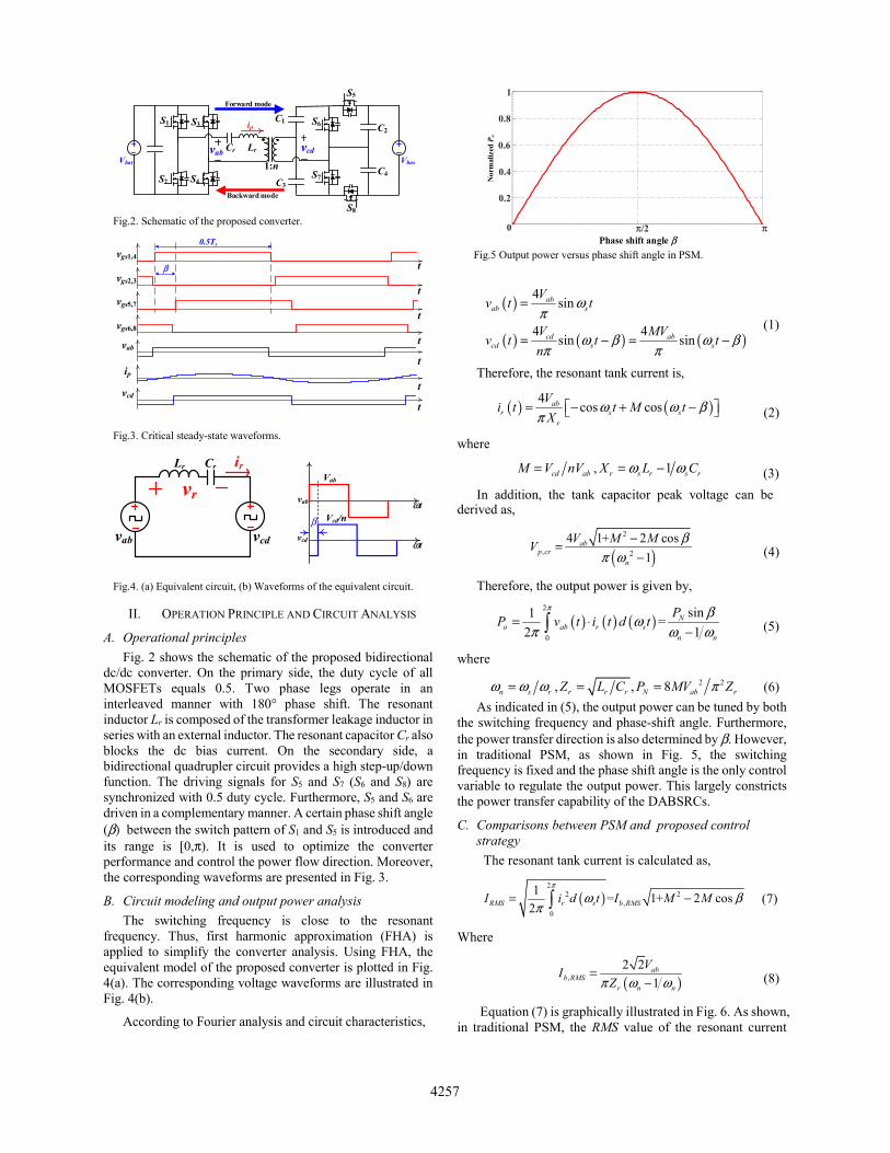
Fig. 2 shows the schematic of the proposed bidirectional dc/dc converter. On the primary side, the duty cycle of all MOSFETs equals 0.5. Two phase legs operate in an interleaved manner with 180° phase shift. The resonant inductor Lr is composed of the transformer leakage inductor in series with an external inductor. The resonant capacitor Cr also blocks the dc bias current. On the secondary side, a bidirectional quadrupler circuit provides a high step-up/down function. The driving signals for S5 and S7 (S6 and S8) are synchronized with 0.5 duty cycle. Furthermore, S5 and S6 are driven in a complementary manner. A certain phase shift angle (β) between the switch pattern of S1 and S5 is introduced and its range is [0,π). It is used to optimize the converter performance and control the power flow direction. Moreover, the corresponding waveforms are presented in Fig. 3.
B. Circuit modeling and output power analysis
The switching frequency is close to the resonant frequency. Thus, first harmonic approximation (FHA) is applied to simplify the converter analysis. Using FHA, the equivalent model of the proposed converter is plotted in Fig. 4(a). The corresponding voltage waveforms are illustrated in Fig. 4(b).
According to Fourier analysis and circuit characteristics,
( )
( ) ( ) ( )
4sin
4 4sin sin
abab s
cd abcd s s
Vv t t
V MVv t t t
n
ωπ
ω β ω βπ π
=
= − = − (1)
Therefore, the resonant tank current is,
( ) ( )4cos cosab
r s sr
Vi t t M t
Xω ω β
π= − + − (2)
where
, 1cd ab r s r s rM V nV X L Cω ω= = − (3)
In addition, the tank capacitor peak voltage can be derived as,
( )2
, 2
4 1+ 2 cos
1ab
p cr
n
V M MV
βπ ω
−=−
(4)
Therefore, the output power is given by,
( ) ( ) ( )2
0
sin1=
2 1N
o ab r sn n
PP v t i t d t
π βωπ ω ω
= ⋅− (5)
where
2 2, , 8n s r r r r N ab rZ L C P MV Zω ω ω π= = = (6)
As indicated in (5), the output power can be tuned by both the switching frequency and phase-shift angle. Furthermore, the power transfer direction is also determined by β. However, in traditional PSM, as shown in Fig. 5, the switching frequency is fixed and the phase shift angle is the only control variable to regulate the output power. This largely constricts the power transfer capability of the DABSRCs.
C. Comparisons between PSM and proposed control strategy
The resonant tank current is calculated as,
( )
22 2
,
0
1= 1+ 2 cos
2RMS r s b RMSI i d t I M Mπ
ω βπ
= − (7)
Where
( ),
2 2
1ab
b RMSr n n
VI
Zπ ω ω=
− (8)
Equation (7) is graphically illustrated in Fig. 6. As shown, in traditional PSM, the RMS value of the resonant current
S4
S3
S2
S1
vab
1:n
vcdLr
Vbat
C2
C4
ipC1
C3
S6
S7
Cr
S5
S8
Forward mode
Backward mode
Vbus
Fig.2. Schematic of the proposed converter.
vgs1,4t
0.5Ts
vgs2,3
vgs5,7
vgs6,8
vab
ip
vcd
t
t
t
t
t
t
β
Fig.3. Critical steady-state waveforms.
vab
Lr ir
vcd
Cr
vcd ωt
vab
βωt
Vab
Vcd/n
vr
Fig.4. (a) Equivalent circuit, (b) Waveforms of the equivalent circuit.
0 π/2 π
0.2
0.4
0.6
0.8
1
Phase shift angle β
Nor
mal
ized
Po
Fig.5 Output power versus phase shift angle in PSM.
4257
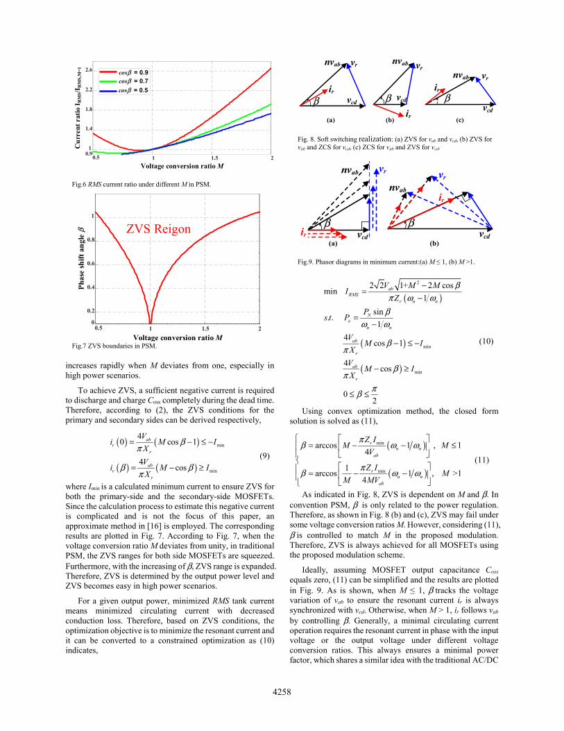
increases rapidly when M deviates from one, especially in high power scenarios.
To achieve ZVS, a sufficient negative current is required to discharge and charge Coss completely during the dead time. Therefore, according to (2), the ZVS conditions for the primary and secondary sides can be derived respectively,
( ) ( ) min
40 cos 1ab
rr
Vi M I
Xβ
π= − ≤ −
( ) ( ) min
4cosab
rr
Vi M I
Xβ β
π= − ≥
(9)
where Imin is a calculated minimum current to ensure ZVS for both the primary-side and the secondary-side MOSFETs. Since the calculation process to estimate this negative current is complicated and is not the focus of this paper, an approximate method in [16] is employed. The corresponding results are plotted in Fig. 7. According to Fig. 7, when the voltage conversion ratio M deviates from unity, in traditional PSM, the ZVS ranges for both side MOSFETs are squeezed. Furthermore, with the increasing of β, ZVS range is expanded. Therefore, ZVS is determined by the output power level and ZVS becomes easy in high power scenarios.
For a given output power, minimized RMS tank current means minimized circulating current with decreased conduction loss. Therefore, based on ZVS conditions, the optimization objective is to minimize the resonant current and it can be converted to a constrained optimization as (10) indicates,
( )
( )
( )
2
min
min
2 2 1+ 2 cosmin
1
sin. .
1
4 cos 1
4 cos
02
abRMS
r n n
No
n n
ab
r
ab
r
V M MI
Z
Ps t P
VM I
X
VM I
X
βπ ω ω
βω ω
βπ
βπ
πβ
−=
−
=−
− ≤ −
− ≥
≤ ≤
(10)
Using convex optimization method, the closed form solution is solved as (11),
( )
( )
min
min
arccos 1 , 14
1arccos 1 , >1
4
rn n
ab
rn n
ab
Z IM M
V
Z IM
M MV
πβ ω ω
πβ ω ω
= − − ≤
= − −
(11)
As indicated in Fig. 8, ZVS is dependent on M and β. In convention PSM, β is only related to the power regulation. Therefore, as shown in Fig. 8 (b) and (c), ZVS may fail under some voltage conversion ratios M. However, considering (11), β is controlled to match M in the proposed modulation. Therefore, ZVS is always achieved for all MOSFETs using the proposed modulation scheme.
Ideally, assuming MOSFET output capacitance Coss equals zero, (11) can be simplified and the results are plotted in Fig. 9. As is shown, when M ≤ 1, β tracks the voltage variation of vab to ensure the resonant current ir is always synchronized with vcd. Otherwise, when M > 1, ir follows vab by controlling β. Generally, a minimal circulating current operation requires the resonant current in phase with the input voltage or the output voltage under different voltage conversion ratios. This always ensures a minimal power factor, which shares a similar idea with the traditional AC/DC
0.5 1 1.5 2
1
1.4
1.8
2.2
2.6
Voltage conversion ratio M
Cu
rren
t ra
tio
I RM
S/I R
MS,
M=
1
0.9
cosβ = 0.7cosβ = 0.5
cosβ = 0.9
Fig.6 RMS current ratio under different M in PSM.
Voltage conversion ratio M
Pha
se s
hif
t an
gle
β
0.5 1 1.5 2
0.2
0.4
0.6
0.8
1
ZVS Reigon
0
Fig.7 ZVS boundaries in PSM.
vr
(a)
vcd
nvab
β ir
vr
vcd
nvab
β ir
vcd
nvab
β ir
(b) (c)
vr
Fig. 8. Soft switching realization: (a) ZVS for vab and vcd, (b) ZVS for vab and ZCS for vcd, (c) ZCS for vab and ZVS for vcd.
(b)(a)vcd
nvab
β ir
vr
vcd
nvab
β
ir
vr
Fig.9. Phasor diagrams in minimum current:(a) M ≤ 1, (b) M >1.
4258
power factor correction. However, it should be noted that the simplified analysis doesn’t ensure a robust ZVS practically.
D. Control strategy
As mentioned above, the output power is affected by the switching frequency and the phase-shift angle. Furthermore, according to (11), to minimize the resonant current and ensure ZVS, the phase-shift angle should track the variation of voltage conversion ratio. Therefore, a new hybrid control strategy, PSM plus VFM, is proposed. The switching frequency regulates the output power. In addition, the phase-shift angle is used to minimize a circulating current and facilitates ZVS under different voltage conversion ratios.
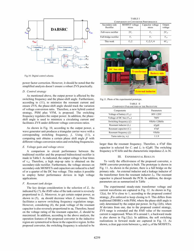
As shown in Fig. 10, according to the output power, a wave generator unit produces a triangular carrier wave with a corresponding switching frequency, fs. Using (11), a computing unit obtains a certain phase shift angle β with different voltage conversion ratios and switching frequencies.
E. Voltage gain and voltage stress
A comparison in circuit performance between the traditional rectifier and the proposed bidirectional rectifier is made in Table I. As indicated, the output voltage is four times of vcd. Therefore, a high step-up ratio is obtained on the secondary-side rectifier. Furthermore, the voltage stresses on secondary-side MOSFETs and capacitors are reduced to a half of or a quarter of the DC bus voltage. This makes it possible to employ better performance devices in high voltage applications.
F. Resonant tank design
The key design consideration is the selection of Zr. As indicated by (7), the RMS value of the tank current is reversely proportional to Zr. Moreover, to get certain output power, as shown in (5), ωn should decrease when Zr increases. This facilitates a narrow switching frequency regulation range. However, considering (4), the peak voltage of the resonant capacitor is also reversely proportional to ωn. Therefore, based on the voltage rating of the resonant capacitor, Zr should be maximized. In addition, according to the above analysis, the operation features of the proposed converter in the inductive region are symmetrical to those in the capacitive region. In this proposed converter, the switching frequency is selected to be
larger than the resonant frequency. Therefore, a 47nF film capacitor is selected for Cr and Lr is 62μH. The switching frequency is 93 kHz and the characteristic impedance Zr is 36.
III. EXPERIMENTAL RESULTS
To verify the effectiveness of the proposed converter, a 500W converter prototype is built. The prototype is shown in Fig. 11. As shown in the picture, there is a full bridge on the primary side. An external inductor and a leakage inductor of the transformer form the resonant inductor LS. The resonant capacitor is placed beneath the PCB. In addition, the design parameters are as summarized in Table �.
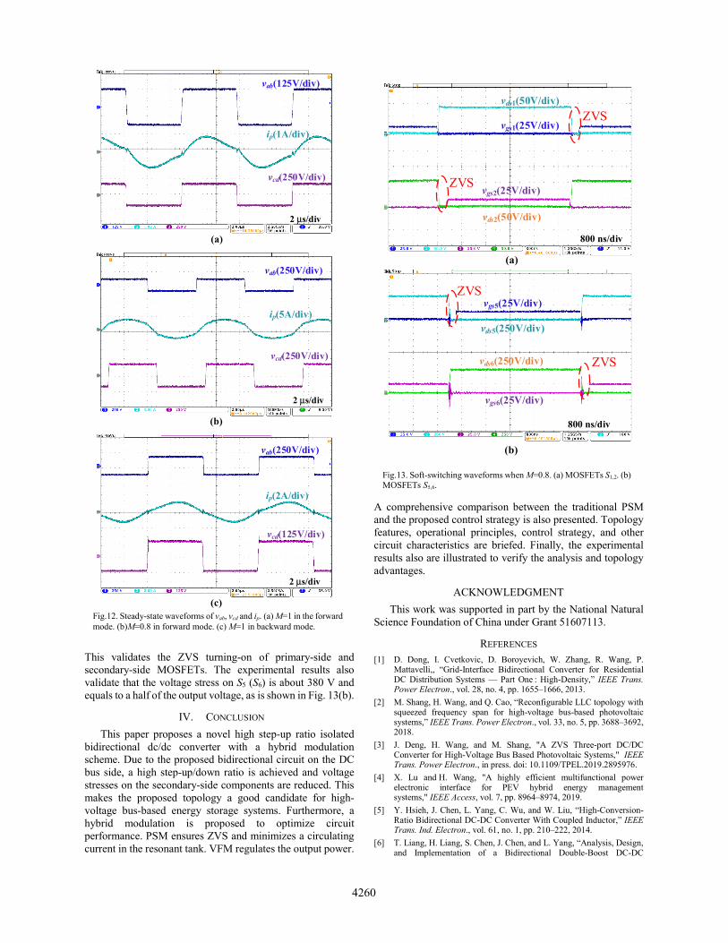
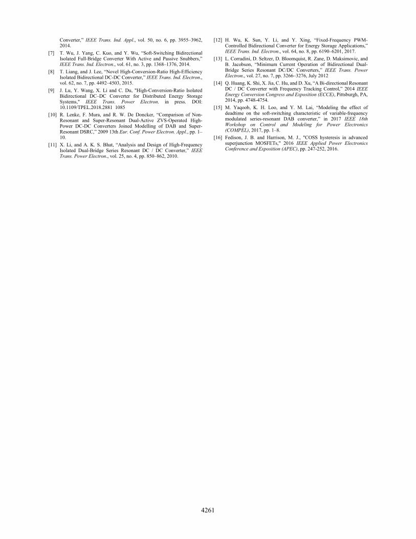
The experimental steady-state transformer voltage and current waveforms are captured in Fig. 12. As shown in Fig. 12(a), for M is close to 1, according to the proposed control strategy, β is enforced to keep closing to 0. This differs from traditional DBSRCs with PSM, where the phase-shift angle is only determined by the output put power. In Fig.12(b), when M deviates from one, due to the proposed control strategy, ZVS range is extended and the RMS value of the resonant current is suppressed. When M is around 1, a backward mode is also shown in Fig.12(c). In addition, the soft switching realizations in forward mode are captured in Fig. 13. As shown, a clear gap exists between vgs and vds of the MOSFETs.
TABLE I COMPARISON OF CONVERTER PERFORMANCE
Secondary-side Rectifier
MOSFET voltage stress
Capacitor voltage stress
Output voltage
Full-wave rectifier 2Vo Vo 2Vcd
Full-bridge rectifier Vo Vo Vcd
This work Vo/2 Vo/2,Vo/4 4Vcd
DC bus side
Battery sideTransformer
External inductor
Fig.11. Photo of the experimental prototype.
TABLE II COMPONENT PARAMETERS OF THE PROTOTYPE
Components Parameters
Voltage of battery (Vbat) 80V-120V
Voltage of DC bus (Vbus) 760V
Switching frequency (fs) 95kHz-120kHz
Resonant inductor (Lr) 62μH
Resonant capacitor (Cr) 47nF
Resonant frequency (fs) 93kHz
Turns ratio (np: ns) 1:1.9
DABSRC
vbat
fs
IOref
Σ
Vbat Vbus
Wave Generator Unit
io
ComputingUnit
β
Vbus fs
Phase shift Unit
>=
>=
0.5vtri
S1,4
S2,3
S5,7
S6,8
Fig.10. Digital control scheme.
4259
This validates the ZVS turning-on of primary-side and secondary-side MOSFETs. The experimental results also validate that the voltage stress on S5 (S6) is about 380 V and equals to a half of the output voltage, as is shown in Fig. 13(b).
IV. CONCLUSION
This paper proposes a novel high step-up ratio isolated bidirectional dc/dc converter with a hybrid modulation scheme. Due to the proposed bidirectional circuit on the DC bus side, a high step-up/down ratio is achieved and voltage stresses on the secondary-side components are reduced. This makes the proposed topology a good candidate for high-voltage bus-based energy storage systems. Furthermore, a hybrid modulation is proposed to optimize circuit performance. PSM ensures ZVS and minimizes a circulating current in the resonant tank. VFM regulates the output power.
A comprehensive comparison between the traditional PSM and the proposed control strategy is also presented. Topology features, operational principles, control strategy, and other circuit characteristics are briefed. Finally, the experimental results also are illustrated to verify the analysis and topology advantages.
ACKNOWLEDGMENT
This work was supported in part by the National Natural Science Foundation of China under Grant 51607113.
REFERENCES [1] D. Dong, I. Cvetkovic, D. Boroyevich, W. Zhang, R. Wang, P.
Mattavelli,, “Grid-Interface Bidirectional Converter for Residential DC Distribution Systems — Part One : High-Density,” IEEE Trans. Power Electron., vol. 28, no. 4, pp. 1655–1666, 2013.
[2] M. Shang, H. Wang, and Q. Cao, “Reconfigurable LLC topology with squeezed frequency span for high-voltage bus-based photovoltaic systems,” IEEE Trans. Power Electron., vol. 33, no. 5, pp. 3688–3692, 2018.
[3] J. Deng, H. Wang, and M. Shang, "A ZVS Three-port DC/DC Converter for High-Voltage Bus Based Photovoltaic Systems," IEEE Trans. Power Electron., in press. doi: 10.1109/TPEL.2019.2895976.
[4] X. Lu and H. Wang, "A highly efficient multifunctional power electronic interface for PEV hybrid energy management systems," IEEE Access, vol. 7, pp. 8964–8974, 2019.
[5] Y. Hsieh, J. Chen, L. Yang, C. Wu, and W. Liu, “High-Conversion-Ratio Bidirectional DC-DC Converter With Coupled Inductor,” IEEE Trans. Ind. Electron., vol. 61, no. 1, pp. 210–222, 2014.
[6] T. Liang, H. Liang, S. Chen, J. Chen, and L. Yang, “Analysis, Design, and Implementation of a Bidirectional Double-Boost DC-DC
vgs1(25V/div)
vds1(50V/div)
vgs2(25V/div)
800 ns/div
vds2(50V/div)
ZVS
ZVS
vgs5(25V/div)
vds5(250V/div)
vgs6(25V/div)
vds6(250V/div)
800 ns/div
ZVS
ZVS
(b)
(a)
Fig.13. Soft-switching waveforms when M=0.8. (a) MOSFETs S1,2. (b) MOSFETs S5,6.
vab(250V/div)
vcd(250V/div)
ip(5A/div)
2 μs/div
vab(125V/div)
vcd(250V/div)
ip(1A/div)
2 μs/div
(b)
(a)
vab(250V/div)
vcd(125V/div)
ip(2A/div)
2 μs/div
(c) Fig.12. Steady-state waveforms of vab, vcd and ip. (a) M=1 in the forward mode. (b)M=0.8 in forward mode. (c) M=1 in backward mode.
4260
Converter,” IEEE Trans. Ind. Appl., vol. 50, no. 6, pp. 3955–3962, 2014.
[7] T. Wu, J. Yang, C. Kuo, and Y. Wu, “Soft-Switching Bidirectional Isolated Full-Bridge Converter With Active and Passive Snubbers,” IEEE Trans. Ind. Electron., vol. 61, no. 3, pp. 1368–1376, 2014.
[8] T. Liang, and J. Lee, “Novel High-Conversion-Ratio High-Efficiency Isolated Bidirectional DC-DC Converter,” IEEE Trans. Ind. Electron., vol. 62, no. 7, pp. 4492–4503, 2015.
[9] J. Lu, Y. Wang, X. Li and C. Du, "High-Conversion-Ratio Isolated Bidirectional DC–DC Converter for Distributed Energy Storage Systems," IEEE Trans. Power Electron. in press. DOI: 10.1109/TPEL.2018.2881 1085
[10] R. Lenke, F. Mura, and R. W. De Doncker, “Comparison of Non-Resonant and Super-Resonant Dual-Active ZVS-Operated High-Power DC-DC Converters Joined Modelling of DAB and Super-Resonant DSRC,” 2009 13th Eur. Conf. Power Electron. Appl., pp. 1–10.
[11] X. Li, and A. K. S. Bhat, “Analysis and Design of High-Frequency Isolated Dual-Bridge Series Resonant DC / DC Converter,” IEEE Trans. Power Electron., vol. 25, no. 4, pp. 850–862, 2010.
[12] H. Wu, K. Sun, Y. Li, and Y. Xing, “Fixed-Frequency PWM-Controlled Bidirectional Converter for Energy Storage Applications,” IEEE Trans. Ind. Electron., vol. 64, no. 8, pp. 6190–6201, 2017.
[13] L. Corradini, D. Seltzer, D. Bloomquist, R. Zane, D. Maksimovic, and B. Jacobson, “Minimum Current Operation of Bidirectional Dual-Bridge Series Resonant DC/DC Converters,” IEEE Trans. Power Electron., vol. 27, no. 7, pp. 3266–3276, July 2012
[14] Q. Huang, K. Shi, X. Jia, C. Hu, and D. Xu, “A Bi-directional Resonant DC / DC Converter with Frequency Tracking Control,” 2014 IEEE Energy Conversion Congress and Exposition (ECCE), Pittsburgh, PA, 2014, pp. 4748-4754.
[15] M. Yaqoob, K. H. Loo, and Y. M. Lai, “Modeling the effect of deadtime on the soft-switching characteristic of variable-frequency modulated series-resonant DAB converter,” in 2017 IEEE 18th Workshop on Control and Modeling for Power Electronics (COMPEL), 2017, pp. 1–8.
[16] Fedison, J. B. and Harrison, M. J., "COSS hysteresis in advanced superjunction MOSFETs," 2016 IEEE Applied Power Electronics Conference and Exposition (APEC), pp. 247-252, 2016.
4261