hp 83205a cellular adapter assembly level repair
TRANSCRIPT
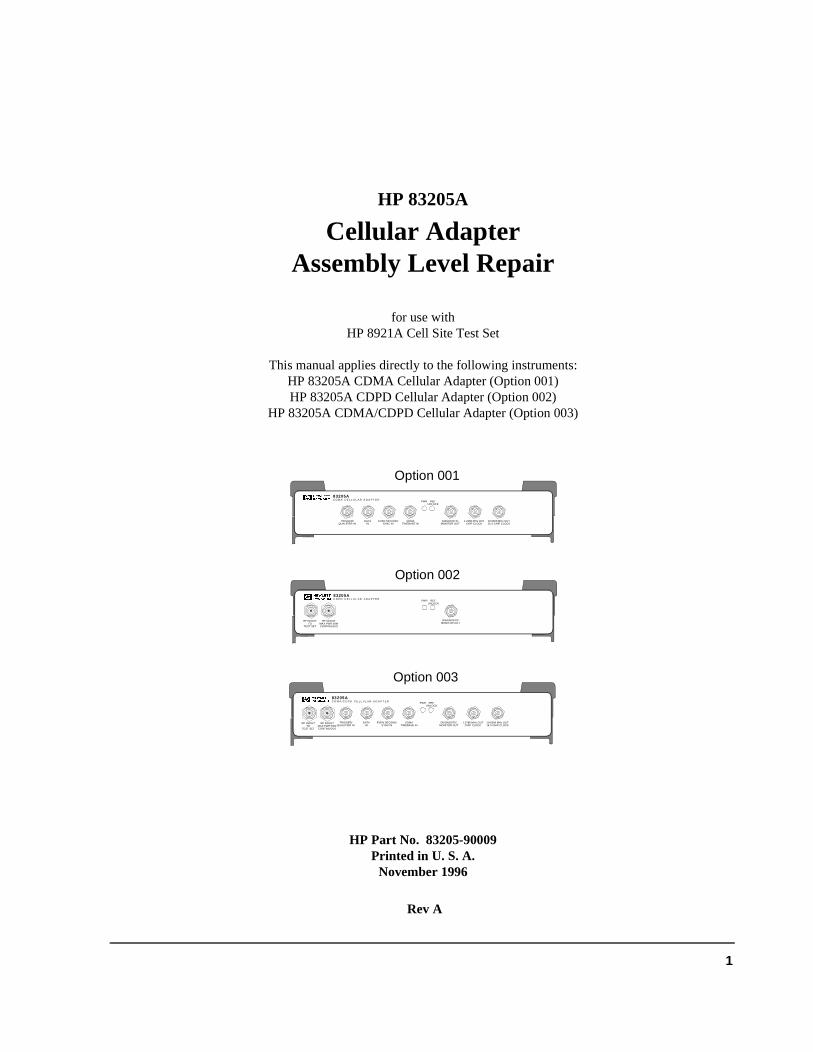
HP 83205A
Cellular AdapterAssembly Level Repair
for use withHP 8921A Cell Site Test Set
This manual applies directly to the following instruments:HP 83205A CDMA Cellular Adapter (Option 001) HP 83205A CDPD Cellular Adapter (Option 002)
HP 83205A CDMA/CDPD Cellular Adapter (Option 003)
HP Part No. 83205-90009Printed in U. S. A.
November 1996
Rev A
Option 003
PWR REFUNLOCK
DIAGNOSTICMONITOR OUT
1.2288 MHz OUTCHIP CLOCK
19.6608 MHz OUT16 X CHIP CLOCK
RF IN/OUTTO
TEST SET
RF IN/OUTMAX.PWR 60WCONTINUOUS
83205AC D M A / C D P D C E L L U L A R A D A P T E R
CDMATIMEBASE IN
EVEN SECOND/SYNC IN
DATAIN
TRIGGER/QUALIFIER IN
Option 002
PWR REFUNLOCK
DIAGNOSTICMONITOR OUT
1.2288 MHz OUTCHIP CLOCK
19.6608 MHz OUT16 X CHIP CLOCK
RF IN/OUTTO
TEST SET
RF IN/OUTMAX.PWR 60WCONTINUOUS
83205AC D P D C E L L U L A R A D A P T E R
CDMATIMEBASE IN
EVEN SECOND/SYNC IN
DATAIN
TRIGGER/QUALIFIER IN
Option 001
PWR REFUNLOCK
DIAGNOSTICMONITOR OUT
1.2288 MHz OUTCHIP CLOCK
19.6608 MHz OUT16 X CHIP CLOCK
RF IN/OUTTO
TEST SET
RF IN/OUTMAX.PWR 60WCONTINUOUS
83205AC D M A C E L L U L A R A D A P T E R
CDMATIMEBASE IN
EVEN SECOND/SYNC IN
DATAIN
TRIGGER/QUALIFIER IN
1

Copyright © Hewlett-Packard Company 1996
2

Notice
Information contained in this document is subject to change without notice.
All Rights Reserved. Reproduction, adaptation, or translation without prior written permission is prohibited, except as allowed under the copyright laws.
This material may be reproduced by or for the U.S. Government pursuant to the Copyright License under the clause at DFARS 52.227-7013 (APR 1988).
Hewlett-Packard CompanyLearning Products Department24001 E. MissionLiberty Lake, WA 99019-9599U.S.A.
3

Manufacturer’s Declaration
This statement is provided to comply with the requirements of the German Sound Emission Directive, from 18 January 1991.
This product has a sound pressure emission (at the operator position) < 70 dB(A).
• Sound Pressure Lp < 70 dB(A).• At Operator Position.• Normal Operation.• According to ISO 7779:1988/EN 27779:1991 (Type Test).
Herstellerbescheinigung
Diese Information steht im Zusammenhang mit den Anforderungen der Maschinenlärminformationsverordnung vom 18 Januar 1991.
• Schalldruckpegel Lp < 70 dB(A).• Am Arbeitsplatz.• Normaler Betrieb.• Nach ISO 7779:1988/EN 27779:1991 (Typprüfung).
4

Safety Considerations
GENERAL
This product and related documentation must be reviewed for familiarization with safety markings and instructions before operation.
This product has been designed and tested in accordance with IEC Publication 1010, "Safety Requirements for Electronic Measuring Apparatus," and has been supplied in a safe condition. This instruction documentation contains information and warnings which must be followed by the user to ensure safe operation and to maintain the product in a safe condition.
SAFETY EARTH GROUND
A uninterruptible safety earth ground must be provided from the main power source to the product input wiring terminals, power cord, or supplied power cord set.
CHASSIS GROUND TERMINAL
To prevent a potential shock hazard, always connect the rear-panel chassis ground terminal to earth ground when operating this instrument from a D.C. power source.
SAFETY SYMBOLS
Indicates instrument damage can occur if indicated operating limits are exceeded. Refer to instruction in this guide.
Indicates hazardous voltages.
Indicates earth (ground) terminal
WARNING: A WARNING note denotes a hazard. It calls attention to a procedure, practice, or thelike, which, if not correctly performed or adhered to, could result in personal injury.Do not proceed beyond a WARNING sign until the indicated conditions are fullyunderstood and met.
CAUTION: A CAUTION note denotes a hazard. It calls attention to an operation procedure, practice,or the like, which, if not correctly performed or adhered to, could result in damage to ordestruction of part or all of the product. Do not proceed beyond an CAUTION note untilthe indicated conditions are fully understood and met.
!
5

Safety Considerations for this Instrument
WARNING This product is a Safety Class I instrument (provided with a protective earthing ground incorporated in the power cord). The mains plug shall only be inserted in a socket outlet provided with a protective earth contact. Any interruption of the protective conductor inside or outside of the product is likely to make the product dangerous. Intentional interruption is prohibited.
Whenever it is likely that the protection has been impaired, the instrument must be made inoperative and be secured against any unintended operation.
If this instrument is to be energized via an autotransformer (for voltage reduction), make sure the common terminal is connected to the earth terminal of the power source.
If this product is not used as specified, the protection provided by the equipment could be impaired. This product must be used in a normal condition (in which all means for protection are intact) only.
No operator serviceable parts are in this product. Refer servicing to qualified personnel. To prevent electrical shock, do not remove covers.
Servicing instructions are for use by qualified personnel only. To avoid electrical shock, do not perform any servicing unless you are qualified to do so.
The opening of covers or removal of parts is likely to expose dangerous voltages. Disconnect the product from all voltage sources while it is being opened.
Adjustments described in the manual are performed with power supplied to the instrument while protective covers are removed. Energy available at many points may, if contacted, result in personal injury.
The power cord is connected to internal capacitors that my remain live for 5 seconds after disconnecting the plug from its power supply.
For continued protection against fire hazard, replace the line fuse(s) only with 250 V fuse(s) or the same current rating and type (for example, normal blow or time delay). Do not use repaired fuses or short circuited fuseholders.
6
C for is
CAUTION: Always use the three-prong A.C. power cord supplied with this product. Failure to ensure adequate earth grounding by not using this cord may cause product damage.
This product is designed for use in Installation Category II and Pollution Degree2 per IEC 1010 and IEC 664 respectively. For indoor use only.
This product has autoranging line voltage input, be sure the supply voltage is within the specified range.
Ventilation Requirements: When installing the product in a cabinet, the convection into and out of the product must not be restricted. The ambient temperature (outside the cabinet) must be less than the maximum operating temperature of the product by 4°every 100 watts dissipated in the cabinet. If the total power dissipated in the cabinetgreater than 800 watts, then forced convection must be used.
Product Markings
CE - the CE mark is a registered trademark of the European Community. A CE mark accompanied by a year indicates the year the design was proven.
CSA - the CSA mark is a registered trademark of the Canadian Standards Association.
7

CERTIFICATION
Hewlett-Packard Company certifies that this product met its published specifications at the time of shipment from the factory. Hewlett-Packard further certifies that its calibration measurements are traceable to the United States National Institute of Standards and Technology, to the extent allowed by the Institute’s calibration facility, and to the calibration facilities of other International Standards Organization members.
WARRANTY
This Hewlett-Packard instrument product is warranted against defects in material and workmanship for a period of one year from date of shipment. During the warranty period, Hewlett-Packard Company will at its option, either repair or replace products which prove to be defective.
For warranty service or repair, this product must be returned to a service facility designated by HP. Buyer shall prepay shipping charges to HP and HP shall pay shipping charges, duties, and taxes for products returned to HP from another country.
HP warrants that its software and firmware designated by HP for use with an instrument will execute its programming instructions when properly installed on that instrument. HP does not warrant that the operation of the instrument, or software, or firmware will be uninterrupted or error free.
LIMITATION OF WARRANTY
The foregoing warranty shall not apply to defects resulting from improper or inadequate maintenance by Buyer, Buyer-supplied software or interfacing, unauthorized modification or misuse, operation outside of the environmental specifications for the product, or improper site preparation or maintenance.
NO OTHER WARRANTY IS EXPRESSED OR IMPLIED. HP SPECIFICALLY DISCLAIMS THE IMPLIED WARRANTIES OF MERCHANTABILITY AND FITNESS FOR A PARTICULAR PURPOSE.
EXCLUSIVE REMEDIES
THE REMEDIES PROVIDED HEREIN ARE BUYER’S SOLE AND EXCLUSIVE REMEDIES. HP SHALL NOT BE LIABLE FOR ANY DIRECT, INDIRECT, SPECIAL, INCIDENTAL, OR CONSEQUENTIAL DAMAGES, WHETHER BASED ON CONTRACT, TORT, OR ANY OTHER LEGAL THEORY.
ASSISTANCE
Product maintenance agreements and other customer assistance agreements are available for Hewlett-Packard products. For any assistance, contact your nearest Hewlett-Packard Sales and Service Office.
8

European Contact: Your local Hewlett-Packard Sales and Service Office or Hewlett-Packard GmbH,Department ZQ/Standards Europe, Herrenberger Strasse 130, D-71034 Böblinger, Germany (FAX+49-7031-14-3143)
DECLARATION OF CONFORMITY according to ISO/IEC Guide 22 and EN 45014
Manufacturer’s Name:
Manufacturer’s Address:
declares that the product
Product Name:
Model Number:
Product Options:
Hewlett-Packard Co.
Spokane Division24001 E. Mission AvenueLiberty Lake, Washington 99019-9599USA
CDMA, CDPD, CDMA/CDPD Cellular Adapter
HP 83205A
This declaration covers all options of the above product.
conforms to the following Product specifications:
Safety: IEC 1010-1:1990+A1 / EN 61010-1:1993
EMC: CISPR 11:1990 / EN 55011:1991 Group 1, Class AEN 50082-1 : 1992
IEC 801-2:1991- 4 kV CD, 8 kV ADIEC 801-3:1984 - 3V/mIEC 801-4:1988 - 0.5 kV Sig. Lines, 1 kV Power Lines
Supplementary Information:
This product herewith complies with the requirements of the Low Voltage Directive 73/23/EEC and the EMC Directive 89/336/EEC and carries the CE-marking accordingly.
Spokane, Washington USA, November 5, 1996Vince Roland,
Reliability & RegulatoryEngineering Manager
9

ady:
t is
HP Support Contacts
The documentation supplied with your Test Set and/or Cellular Adapter is an excellent source of reference, applications, and service information. Please use these manuals if you are experiencing technical problems:
• HP 8920, 8921A Cell Site Test Set’s Assembly Level Repair (ALR) manual, HP part number 08920-90168
• HP 83205A CDMA Cellular Adapter User’s Guide, HP part number 83205-90008
• CDPD Software User’s Guide, HP part number 83204-90014 (for CDPD software kit, HP part number 83204-61807)
If you have used the manuals and still have application questions, contact your local HP Sales Representative.
Repair assistance is available for the HP 8921A Cell Site Test Set and HP 83205A Cellular Adapter from the factory by phone and e-mail. Internal Hewlett-Packard users can contact the factory through HP Desk or cc:Mail© (Lotus Corporation). Parts information is also available from Hewlett-Packard.
When calling or writing for repair assistance, please have the following information re• Instrument model number (HP 83205A)• Instrument Serial Number (tag located on the rear panel).• Installed options - if any (tag located on the rear panel).• Instrument firmware revision (displayed at the top of the screen when the Test Se
powered up, and is also displayed on the CONFIGURE screen).
Support Telephone Numbers:
1 800 827 3848 (Spokane Division Service Assistance, U.S. only) 1 509 921 3848 (Spokane Division Service Assistance, International) 1 800 227 8164 (HP Direct Parts Ordering, U.S. only) 1 916 783 0804 (HP Service Parts Identification, U.S. & Intl.)
Electronic mail (Internet): [email protected]
HP Desk: Spokane Service / HP1000/21
cc:Mail: SERVICE, SPOKANE /HP-Spokane,desk1
10

Table 1 Regional Sales and Service Offices
Eastern USASales OfficeHewlett-Packard Company2101 Gather Rd.Rockville, MD 20850Tel: (301) 258-2000
Eastern USAService CenterHewlett-Packard Company150 Green Pond RoadRockaway, NJ 07866Tel: (201) 586-5400
Midwestern USASales and ServiceHewlett-Packard Company5201 Tollview DriveRolling Meadows, IL 60008Tel: (708) 342-2000
Southern USASales and ServiceHewlett-Packard Company1995 North Park PlaceAtlanta, GA 30339
SalesTel: (404) 955-1500Fax: (404) 980-7292
Service Tel: (404) 850-2544Fax: (404) 980-7292
Southern USAService CenterHewlett-Packard Company930 E. Campbell RoadRichardson, TX 75081Tel: (214) 699-4331
Western USAService CenterHewlett-Packard Company301 E. Evelyn AvenueMountain View, CA 94041Tel: (415) 694-2000Fax: (415) 694-0601
Western USASales and ServiceHewlett-Packard Company24 Inverness Place EastEnglewood, CO 80112
SalesTel: (303) 649-5000Fax: (303) 649-5787
ServiceTel: (303) 649-5512Fax: (303) 649-5787
Western USASales and ServiceHewlett-Packard Company1421 South Manhattan AvenueFullerton, CA 92631
SalesTel: (714) 999-6700Fax: (714) 778-3033
ServiceTel: (714) 758-5490Fax: (714) 778-3033
United States of AmericaCustomer Information CenterHewlett-Packard CompanyTel: (800) 752-0900
6:00 am to 5:00 pm Pacific TimeParts Direct: 1-800-227-8164
South Eastern EuropeSales and ServiceHewlett-Packard Ges. m.b.h.Liebigasse 1P.O. Box 72A-1222 Vienna, Austria
Telephone: 43 222 2500 0Telex: 13 4425
European Multicountry RegionSales and ServiceHewlett-Packard S.A.P.O. Box 95150, Route dv Nant_dl_AVRILCH-1217 Meyrin 2Geneva, Switzerland
Telephone: (41/22) 780-8111Fax: (41/22) 780-8542
Northern EuropeSales and ServiceHewlett-Packard Nederland B.V.Startbaan 161187 XRAmstelveen, The NetherlandsP.O. Box 667
Telephone: 31/20 5476911 X 6631Fax: 31-20-6471825NL
11

AsiaSales and ServiceHewlett-Packard Asia Ltd.22-30/F Peregrine TowerLippo Center89 Queensway, CentralHong KongG.P.O. Box 863 Hong Kong
Telephone: 852-848-7777Fax: 852-868-4997
JapanSales and ServiceYokogawa-Hewlett-Packard Ltd.3-29-21, Takaido-HigashiSuginami-Ku, Tokyo 168
Telephone: 81 3 3331-6111Fax: 81 3 3331-6631
International Sales Branch HeadquartersSales and ServiceHewlett-Packard S.A.39 Rue VeyrotP.O. Box 3651217 Meyrin 1Geneva, Switzerland
Telephone: 41-22-780-4111Fax: 41-22-780-4770
Australia, New ZealandSales and ServiceHewlett-Packard Ltd.P.O. Box 22131-41 Joseph StreetBlackburn, Victoria 3130
Telephone: (61/3) 895-2895Fax: (61/3) 898-9257
CanadaSales and ServiceHewlett-Packard (Canada) Ltd.5150 Spectrum WayMississauga, Ontario L4W 5G1Canada
Telephone: (416) 206-4725Fax: (416) 206-4739
CanadaService CenterHewlett-Packard Company17500 Transcanada HighwayS. Serv RoadKirkland, Quebec H9J 2X8Canada
Telephone: (416) 206-3295
CanadaService CenterHewlett-Packard Ltd.11120 178 StreetEdmonton, Alberta T5S 1P2Canada
Telephone: (403) 486-6666Fax: (403) 489-8764
Latin AmericaHewlett-Packard CompanyLAHQ Mexico CityCol. Lomas de Virreyes11000 Mexico D.F.Mexico
Telephone: (52/5) 326-4000Fax: (52/5) 202 7718
United KingdomSales and ServiceHewlett-Packard Ltd.Cain RoadAmen CornerBracknell, BerkshireRG12 1HNUnited Kingdom
Telephone: 44 344 360000Fax: 44 344 363344
Table 1 Regional Sales and Service Offices (Continued)
12

Power Cables
Plug Type Plug Descriptions
male/female HP Part #
(cable &plug) Cable Descriptions
Straight/Straight 8120-0698 90 inches, black
Used in the following locationsPeru
13

blic,
Plug Type Plug Descriptions
male/female HP Part #
(cable &plug) Cable Descriptions
Straight/Straight Straight/90º
8120-1689 8120-1692
79 inches, mint gray 79 inches, mint gray
Used in the following locationsAfghanistan, Albania, Algeria, Angola, Armenia, Austria, Azerbaijan, Azores
Bangladesh, Belgium, Benin, Bolivia, Boznia-Herzegovina, Bulgaria, Burkina Faso, Burma, Burundi, Byelarus
Cameroon, Canary Islands, Central African Republic, Chad, Chile, Comoros, Congo, Croatia, Czech RepuCzechoslovakia
Denmark, Djibouti
East Germany, Egypt, Estonia, Ethiopia
Finland, France, French Guiana, French Indian Ocean Areas
Gabon, Gaza Strip, Georgia, Germany, Gozo, Greece
Hungary
Iceland, Indonesia, Iran, Iraq, Israel, Italy, Ivory Coast
Jordan
Kazakhstan, Korea, Kyrgystan
Latvia, Lebanon, Libya, Lithuania, Luxembourg
Macedonia, Madeira Islands, Malagasy Republic, Mali, Malta, Mauritania, Miquelon, Moldova, Mongolia, Morocco, Mozambique
Nepal, Netherlands, Netherlands Antilles, Niger, Norway
Oman
Pakistan, Paraguay, Poland, Portugal
Rep. South Africa, Romania, Russia, Rwanda
Saudi Arabia (220V), Senegal, Slovak Republic, Slovenia, Somalia, Spain, Spanish Africa, Sri Lanka, St. Pierre Islands
Sweden, Syria
Tajikistan, Thailand, Togo, Tunisia, Turkey, Turkmenistan
USSR, Ukraine, Uzbekistan
Western Africa, Western Sahara
Yugoslavia
Zaire
14

Plug Type Plug Descriptions
male/female HP Part #
(cable &plug) Cable Descriptions
Straight/Straight Straight/90°
8120-2104 8120-2296
79 inches, gray 79 inches, gray
Used in the following locationsSwitzerland
15
Plug Type Plug Descriptions
male/female HP Part #
(cable &plug) Cable Descriptions
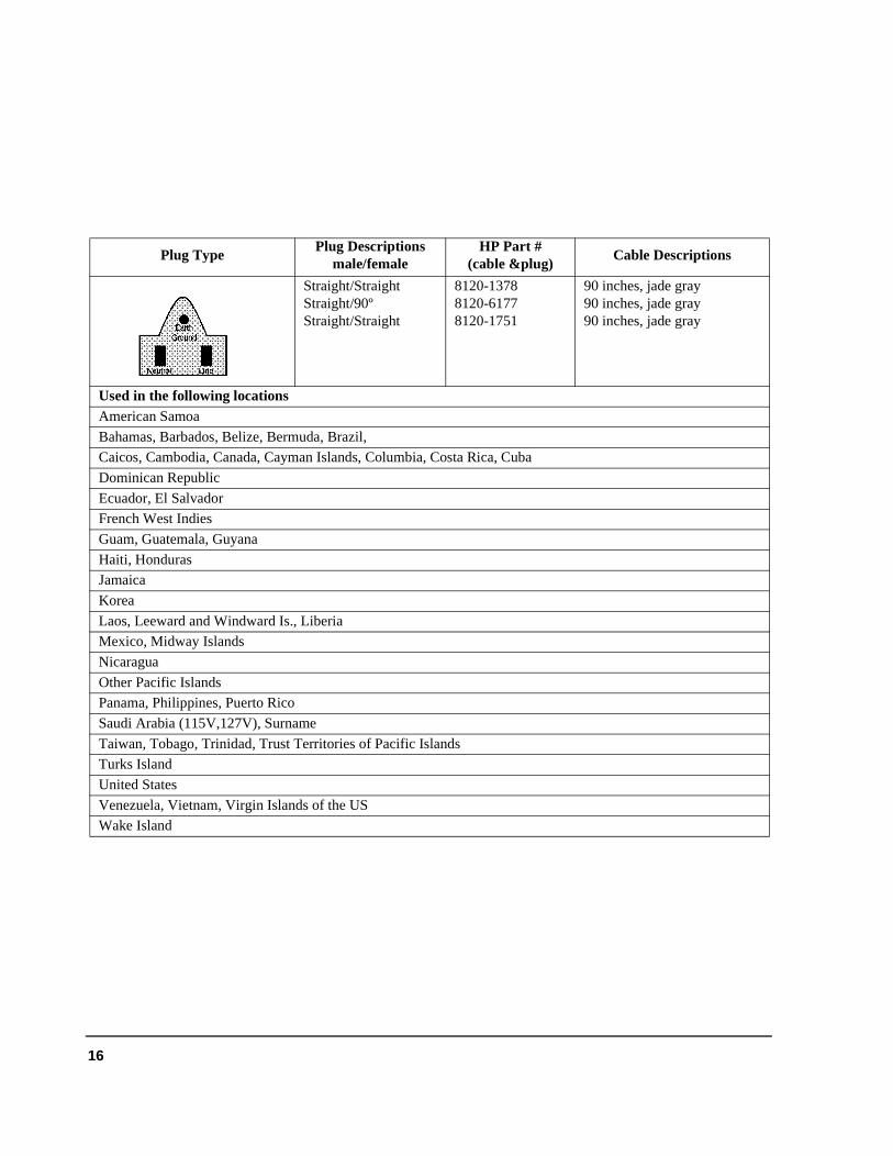
Straight/Straight Straight/90º Straight/Straight
8120-1378 8120-6177 8120-1751
90 inches, jade gray 90 inches, jade gray 90 inches, jade gray
Used in the following locationsAmerican Samoa
Bahamas, Barbados, Belize, Bermuda, Brazil,
Caicos, Cambodia, Canada, Cayman Islands, Columbia, Costa Rica, Cuba
Dominican Republic
Ecuador, El Salvador
French West Indies
Guam, Guatemala, Guyana
Haiti, Honduras
Jamaica
Korea
Laos, Leeward and Windward Is., Liberia
Mexico, Midway Islands
Nicaragua
Other Pacific Islands
Panama, Philippines, Puerto Rico
Saudi Arabia (115V,127V), Surname
Taiwan, Tobago, Trinidad, Trust Territories of Pacific Islands
Turks Island
United States
Venezuela, Vietnam, Virgin Islands of the US
Wake Island
16

Plug Type Plug Descriptions
male/female HP Part #
(cable &plug) Cable Descriptions
Straight/Straight Straight/90º
8120-4753 8120-4754
90 inches, dark gray 90 inches, dark gray
Used in the following locationsJapan
Plug Type Plug Descriptions
male/female HP Part #
(cable &plug) Cable Descriptions
90º/Straight 90º/90º Straight/Straight
8120-2956 8120-2957 8120-3997
79 inches, gray 79 inches, gray 79 inches, gray
Used in the following locationsDenmark
Greenland
Plug Type Plug Descriptions
male/female HP Part #
(cable &plug) Cable Descriptions
Straight/Straight Straight/90°
8120-4211 8120-4600
79 inches, mint gray 79 inches, mint gray
Used in the following locationsBotswanaIndiaLesothoMalawiSouth-West Africa (Namibia), SwazilandZambia, Zimbabwe
17

Plug Type Plug Descriptions
male/female HP Part #
(cable &plug) Cable Descriptions
Straight/Straight Straight/Straight Straight/90º Straight/90º
8120-1860 8120-1575 8120-2191 8120-4379
60 inches, jade gray 30 inches, jade gray 60 inches, jade gray 15.5 inches, jade gray
Used in the following locationsSystem Cabinets
Plug Type (Male) Plug Descriptions
male/female HP Part #
(cable& plug) Cable Descriptions
90°/Straight 90°/90°
8120-1351 8120-1703
90 inches, mint gray 90 inches, mint gray
Used in the following locationsBahrain, British Indian Ocean Territories, BruneiCanton, CyprusEnderbury Island, Equatorial GuineaFalkland Islands, French Pacific IslandsGambia, Ghana, Gibraltar, GuineaHong KongIrelandKenya, KuwaitMacao, Malaysia, MauritiusNigeriaQatarSeychelles, Sierra Leone, Singapore, Southern Asia, Southern Pacific Islands, St. Helena, SudanTanzaniaUganda, United Arab Emirates, United KingdomYeman (Aden & Sana)
18

Plug Type Plug Descriptions
male/female HP Part #
(cable &plug) Cable Descriptions
Straight/Straight Straight/90°
8120-1369 8120-0696
79 inches, gray 80 inches, gray
Used in the following locationsArgentina, Australia
China (People’s Republic)
New Zealand
Papua New Guinea
Uruguay
Western Samoa
19

ATTENTIONStatic Sensitive Devices
This instrument was constructed in an ESD (electro-static discharge) protected environment. This is because most of the semiconductor devices used in this instrument are susceptible to damage by static discharge.
Depending on the magnitude of the charge, device substrates can be punctured or destroyed by contact or mere proximity of a static charge. The result can cause degradation of device performance, early failure, or immediate destruction.
These charges are generated in numerous ways such as simple contact, separation of materials, and normal motions of persons working with static sensitive devices.
When handling or servicing equipment containing static sensitive devices, adequate precautions must be taken to prevent device damage or destruction.
Only those who are thoroughly familiar with industry accepted techniques for handling static sensitive devices should attempt to service circuitry with these devices.
In all instances, measures must be taken to prevent static charge build-up on work surfaces and persons handling the devices.
20

d nd
ntify a the
ting mated
rs for
In This Book
This manual contains the following information to help you repair, calibrate, and verify correct operation of the HP 83205A Cellular Adapter.
Chapter 1, Introduction, on page 29. This chapter provides a general description of the Cellular Adapter and general information concerning troubleshooting, repair, and calibration of the Cellular Adapter. HP service and support information is also provided.
Chapter 2, Troubleshooting, on page 37. This chapter contains the procedures for isolating a failure to the faulty assembly. The Cellular Adapter’s automatediagnostics are described and descriptions are provided to help you understawhat has been checked by the diagnostics in case the diagnostics cannot ideprobable failure. Further investigation may require manually troubleshooting Cellular Adapter.
Chapter 3, Disassembly and Replacement, on page 61. This chapter provides procedures and illustrations for disassembling the Cellular Adapter.
Chapter 4, Modifications, on page 85. This chapter explains how to verify and/or upgrade the firmware in the Cellular Adapter.
Chapter 5, Block Diagrams, on page 89. Diagrams are provided illustrating thegeneral operation of the Cellular Adapter. This information is used to better understand the operation of the Cellular Adapter when manually troubleshoothe Test System (the attached Test Set and Cellular Adapter) in case the autodiagnostics cannot identify a faulty assembly with high confidence.
Chapter 6, Replaceable Parts, on page 105. Contains illustrations for identifying the various assemblies and components of the Cellular Adapter. Part numbeeach replaceable part are also provided.
Chapter 7, Periodic Calibration and Performance Tests, on page 125. Contains Cellular Adapter periodic calibration procedures and performance tests.
Chapter 8, Specifications, on page 139. Lists the warranted specifications of theCellular Adapter.
Glossary, on page 149. Provides a list of common acronyms, terms, and definitions used in cellular communications.
21

Conventions Used in this Manual
The HP 83205A CDMA Cellular Adapter (Option 001), the HP 83205A CDPD Cellular Adapter (Option 002), or the HP 83205A CDMA/CDPD Cellular Adapter (Option 003) is referred to as the Cellular Adapter.
The HP 8921A Cell Site Test Set is referred to as the Test Set.
The Cellular Adapter combined with the Test Set is referred to as the Test System.
Other Manuals Required
In troubleshooting the Cellular Adapter it may be necessary to use the:
• HP 8921A Cell Site Test Set’s ALR manual, HP part number 08920-90168
• HP 83205A CDMA Cellular Adapter User’s Guide, HP part number 83205-90008
• CDPD Software User’s Guide, HP part number 83204-90014 (for CDPD software kit, HP part number 83204-61807)
22
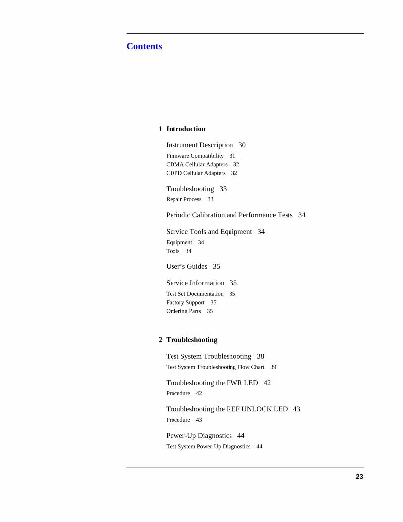
Contents
1 Introduction
Instrument Description 30
Firmware Compatibility 31
CDMA Cellular Adapters 32
CDPD Cellular Adapters 32
Troubleshooting 33
Repair Process 33
Periodic Calibration and Performance Tests 34
Service Tools and Equipment 34
Equipment 34
Tools 34
User’s Guides 35
Service Information 35
Test Set Documentation 35
Factory Support 35
Ordering Parts 35
2 Troubleshooting
Test System Troubleshooting 38
Test System Troubleshooting Flow Chart 39
Troubleshooting the PWR LED 42
Procedure 42
Troubleshooting the REF UNLOCK LED 43
Procedure 43
Power-Up Diagnostics 44
Test System Power-Up Diagnostics 44
23

Contents
Cellular Adapter Power-Up Diagnostics 45
Verifying Test Set Operation 49
Procedure 49
Verifying that the Test Set Recognizes the Cellular Adapter 51
Prerequisites 51
Procedure 51
CDMA Diagnostics 52
Prerequisites 52
CDMA_DIAG Procedure 52
CDMA_DIAG Tests Descriptions 54
CDPD Diagnostics 55
CDPD_DIAG Procedure 56
CDPD_DIAG Tests Descriptions 58
3 Disassembly and Replacement
Disassembly of the HP 83205A Cellular Adapter 62
Separating Units and Removing Cover 63
Operation Without Cover 65
Removing the A8 Power Supply Assembly 66
Disconnecting Subassembly Power Connectors 67
Removing the Front Panel 68
Removing the Rear Panel 70
Removing the A4 Gen/Ref Assembly 72
Removing the A9 Reference/IQ Assembly 74
Removing the A4 and A9 Assemblies as a Unit 76
Removing the A10 Coupler & Switch Assembly and Semi-Rigid Cables 78
Removing the A11 CDPD Assembly 80
Removing the A2 RX DSP and A5 Data Buffer Assemblies 81
Removing the A3 Motherboard Assembly 83
24

Contents
4 Modifications
Firmware Upgrades 86
Firmware Loading and Verification 87
Load the DSP Firmware 87
Load the CDPD Firmware 87
Verifying Firmware Version 88
5 Block Diagrams
Instrument Description 90
CDMA Cellular Adapter 91
CDPD Cellular Adapter 93
Assembly Descriptions 94
A2 RX DSP Assembly 96
A3 Motherboard 96
A4 Gen/Ref Assembly 96
A5 Data Buffer Modulator 98
A8 Power Supply 98
A9 Reference/ IQ 98
A10 Directional Coupler & Serial Switch 100
A11 CDPD Assembly 100
Power Supply and Voltage Distribution 102
6 Replaceable Parts
Parts Identification 106
Major Assemblies 106
CDPD Components 107
External Cables 108
25

Contents
Front Panel Components 109
Cover and Rear Panel Components 110
Rear Panel Components 111
Miscellaneous Components 112
A4 Gen./Ref. Assembly and Components 113
A9 Reference/IQ Assembly 114
A10 Directional Coupler & Serial Switch Assembly 115
A11 CDPD Assembly 116
Semi-Rigid Cables & Components 117
A2 RX DSP Assembly 118
A5 Data Buffer Assembly 118
A3 Motherboard Assembly 119
Parts List 120
7 Periodic Calibration and Performance Tests
Introduction 126
Periodic Calibration (for Options 001 & 003 only) 127
PER_CALD Calibration Procedure 127
EBNO_CAL Calibration Procedure 128
CDMA Performance Test (for Options 001 & 003 only) 129
Prerequisites 129
Equipment Setup 129
CDMA Performance Procedure 129
CDPD Performance Test (for Options 002 & 003 only) 131
Prerequisites 131
Equipment Set Up 131
Procedure 131
CDMA Performance Record 137
Rho Measurement 137
CDPD Performance Record 138
26
Contents
CDPD Generator Spectral Purity Measurement 138
CDPD Modulation Accuracy Measurement 138
CDPD Generator On/Off Level Measurement 138
8 Specifications
HP 83205A CDMA Specifications 140
CDMA Signal Generator 140
CDMA Analyzer 142
Code Domain Analyzer 144
RF Time Base 145
CDMA Reference 146
HP 83205A CDPD Specifications 147
CDPD Signal Generator 147
CDPD Analyzer 148
Physical Specifications 148
Glossary 149
Index 181
27

Contents
28

1
Introduction
This chapter contains a general description of the HP 83205A Cellular Adapter, and general information about troubleshooting, calibrating, and servicing the Cellular Adapter. Lists of equipment (including documentation) required to service the Cellular Adapter are also provided.
29

Chapter 1, IntroductionInstrument Description
ly)
Instrument Description
The HP 83205A Cellular Adapter (see figure 1) is an accessory to the HP 8921A Cell Site Test Set. The Cellular Adapter and Test Set are connected together via front-panel and rear-panel cables and work together to form a Test System. The Cellular Adapter adds digital signal generation and analysis to the Test Set’s analog test capabilities.
Figure 1 HP 83205A CDMA/CDPD Cellular Adapter and HP 8921ACell Site Test Set
The HP 83205A Cellular Adapter can be configured as one of three differentoptions (see figure 2 on page 31):• HP 83205A CDMA Cellular Adapter, Option 001• HP 83205A CDPD Cellular Adapter, Option 002• HP 83205A CDMA/CDPD Cellular Adapter, Option 003
Each Cellular Adapter has the following major assemblies: • A2 Receiver Digital Signal Processing (RX DSP)• A3 Motherboard• A4 Generator/Reference• A5 Data Buffer (in Cellular Adapter Options 001 & 003 only)• A8 Power Supply• A9 Reference/IQ (This assembly includes the A6 LO/IF and A7 IQ Modulator
assemblies. These assemblies cannot be separately replaced.)• A10 Directional Coupler & Serial Switch (in Cellular Adapter Options 002 & 003 on• A11 CDPD processor (in Cellular Adapter Options 002 & 003 only)
PWR REFUNLOCK
DIAGNOSTICMONITOR OUT
1.2288 MHz OUTCHIP CLOCK
19.6608 MHz OUT16 X CHIP CLOCKRF IN/OUT
TOTEST SET
RF IN/OUTMAX.PWR 60WCONTINUOUS
83205AC D M A / C D P D C E L L U L A R A D A P T E R
CDMATIMEBASE IN
EVEN SECOND/SYNC IN
DATAIN
TRIGGER/QUALIFIER IN
HP 83205ACDMA/CDPD
HP 8921A Cell SiteTest Set
(Option 003)Cellular Adapter
30

Chapter 1, IntroductionInstrument Description
Figure 2 HP 83205A Cellular Adapter Options
Firmware Compatibility
In order for the Cellular Adapter to operate properly, it is necessary that its companion Test Set have the proper firmware installed. See "Verifying Firmware Version" on page 88 for the firmware requirements of the Test Set.
HP 83205A CDMACellular Adapter, Option 001
HP 83205A CDPDCellular Adapter, Option 002
HP 83205A CDMA/CDPDCellular Adapter, Option 003
Front Back114.3 MHz IF IN I BASEBAND OUT
AUXCWRF IN
IQRF OUT OPTIONAL
SE
RIA
L P
OR
T
CONTROL I/OSYNTH REF IN 10 MHz OUT
CDMA CLOCK OUTPUTS DSP IN
MOD OUT
10 MHzREF OUT
Q BASEBAND OUT
PWR REFUNLOCK
DIAGNOSTICMONITOR OUT
1.2288 MHz OUTCHIP CLOCK
19.6608 MHz OUT16 X CHIP CLOCK
RF IN/OUTTO
TEST SET
RF IN/OUTMAX.PWR 60WCONTINUOUS
83205AC D M A / C D P D C E L L U L A R A D A P T E R
CDMATIMEBASE IN
EVEN SECOND/SYNC IN
DATAIN
TRIGGER/QUALIFIER IN
Front Back114.3 MHz IF IN I BASEBAND OUT
AUXCWRF IN
IQRF OUT OPTIONAL
SE
RIA
L P
OR
T
CONTROL I/OSYNTH REF IN 10 MHz OUT
CDMA CLOCK OUTPUTS DSP IN
MOD OUT
10 MHzREF OUT
Q BASEBAND OUT
PWR REFUNLOCK
DIAGNOSTICMONITOR OUT
1.2288 MHz OUTCHIP CLOCK
19.6608 MHz OUT16 X CHIP CLOCK
RF IN/OUTTO
TEST SET
RF IN/OUTMAX.PWR 60WCONTINUOUS
83205AC D P D C E L L U L A R A D A P T E R
CDMATIMEBASE IN
EVEN SECOND/SYNC IN
DATAIN
TRIGGER/QUALIFIER IN
Front Back114.3 MHz IF IN I BASEBAND OUT
AUXCWRF IN
IQRF OUT OPTIONAL
SE
RIA
L P
OR
T
CONTROL I/OSYNTH REF IN 10 MHz OUT
CDMA CLOCK OUTPUTS DSP IN
MOD OUT
10 MHzREF OUT
Q BASEBAND OUT
PWR REFUNLOCK
DIAGNOSTICMONITOR OUT
1.2288 MHz OUTCHIP CLOCK
19.6608 MHz OUT16 X CHIP CLOCK
RF IN/OUTTO
TEST SET
RF IN/OUTMAX.PWR 60WCONTINUOUS
83205AC D M A C E L L U L A R A D A P T E R
CDMATIMEBASE IN
EVEN SECOND/SYNC IN
DATAIN
TRIGGER/QUALIFIER IN
31
Chapter 1, IntroductionInstrument Description
CDMA Cellular Adapters
The HP 83205A CDMA Cellular Adapter (Option 001) and the HP 83205A CDMA/CDPD Cellular Adapter (Option 003) include DSP (Digital Signal Processing) hardware and firmware to test the transmitter and receiver portions of Code Division Multiple Access (CDMA) base stations. Systems using the CDMA format use encoders and decoders to digitize speech and add call processing information.
CDMA digital cellular systems use frequency channelization (comparable to current analog systems but with a much wider bandwidth) and correlative codes to distinguish each user. This scheme allows communication in the presence of interference (such as other users) resulting in a substantial increase in system capacity.
CDPD Cellular Adapters
The HP 83205A CDPD Cellular Adapter (Option 002) and the HP 83205A CDMA/CDPD Cellular Adapter (Option 003) include Cellular Digital Packet Data (CDPD) digital signal generation and analysis. The CDPD assembly (A11) found in Cellular Adapter Options 002 and 003 provides the hardware and firmware to perform CDPD protocol processing.
CDPD is a packet data system which overlies the existing Advanced Mobile Phone System (AMPS) voice system. CDPD is designed for small bursts of data and is not efficient for large file transfer applications. CDPD uses a separate base station (Mobile Data Base Station, MDBS) and is integrated into the antenna system of a cell site. When there is no voice traffic on a designated AMPS voice channel, the MDBS may transmit packet data to mobile end stations or fixed end stations. When AMPS voice traffic is assigned to that channel, the MDBS must power down and reacquire communications on another designated CDPD channel if one is available.
32

Chapter 1, IntroductionTroubleshooting
est
’s
r ics
s the e 37
As-
2,
page
dic
on
Troubleshooting
The Cellular Adapter is normally sent in for service connected to its companion Test Set. The Test Set’s internal ROM contains programs for verifying the Cellular Adapter’s performance and for calibrating the Cellular Adapter and TSet interface.
Diagnostic programs for servicing the Cellular Adapter reside in the Test Setfirmware (ROM). Two types of built-in diagnostics are available to aid in troubleshooting: power-up diagnostics which check the Test Set and CellulaAdapter’s internal control circuitry, and CDMA and CDPD functional diagnostwhich check analog and digital signal generation and analysis.
Chapter 7, "Periodic Calibration and Performance Tests" on page 125 explaincalibration and performance programs. Chapter 2, "Troubleshooting" on pagexplains the power-up, CDMA, and CDPD diagnostic programs.
Repair Process Repair of the Cellular Adapter consists of the following steps:
1. Isolate the fault or problem to the Cellular Adapter or the Test Set (see chapter 2, "Trou-bleshooting" on page 37). If the problem is with the Test Set, refer to the Test Set’ssembly Level Repair Manual (08920-90168).
2. Isolate the problem to a faulty assembly within the Cellular Adapter (see chapter"Troubleshooting" on page 37).
3. Replace the faulty assembly (see chapter 3, "Disassembly and Replacement" on61).
4. Calibrate the Test System by regenerating calibration data (see chapter 7, "PerioCalibration and Performance Tests" on page 125).
5. Verify the performance of the Cellular Adapter (see chapter 7, "Periodic Calibratiand Performance Tests" on page 125).
33

Chapter 1, IntroductionPeriodic Calibration and Performance Tests
t cable et. ns.
be
Periodic Calibration and Performance Tests
Run the automatic self-calibration programs provided in the Test Set to calibrate the Cellular Adapter. These programs, PER_CALD and EBNO_CAL, reside in the Test Set’s ROM as part of its firmware. These calibration programs do norequire external equipment or manual adjustments. However, some external connections are required. Performance tests are also provided in the Test SPerformance tests verify that the Cellular Adapter performs to its specificatioFor calibration and performance procedures, refer to chapter 7, "Periodic Calibration and Performance Tests" on page 125.
NOTE: CALIBRATION INTERVAL
The calibration programs PER_CALD and EBNO_CAL, see "Periodic Calibration (forOptions 001 & 003 only)" on page 127, should be performed anytime the Cellular Adapteris disconnected and re-attached to another Test Set, after any assembly is replaced, or atleast every 12 months.
NOTE PERFORMANCE TEST INTERVAL
The performance tests in chapter 7, "Periodic Calibration and Performance Tests" on page125 should be performed anytime an assembly is replaced, or at least every 24 months.
Service Tools and Equipment
Equipment External equipment is not required for the periodic calibration of the Cellular Adapter or for running the diagnostic routines. If diagnostic routines can not isolate the problem, an oscilloscope, voltmeter, and spectrum analyzer may required for further troubleshooting. A second Cellular Adapter/Test Set is helpful for troubleshooting performance test failures.
Tools The following tools are needed for assembly removal and replacement: • TX-10 Torx screwdriver • 1/4-inch socket wrench • 5/16-inch open-end wrench (for SMC connectors)• 15/64-inch open-end wrench (for SMA connectors)• 9/16-inch open-end wrench (for BNC connectors)• 3/4-inch open-end wrench (for Type-N connectors)
34
Chapter 1, IntroductionUser’s Guides
nted
User’s Guides
The CDMA test screens and the Cellular Adapter’s connections are documein the HP 83205A CDMA Cellular Adapter User’s Guide, HP part number 83205-90008.
CDPD software is documented in the CDPD Software User’s Guide, HP part number 83204-90014.
Service Information
Test Set Documentation
The Cellular Adapter along with a Test Set form a Test System. Servicing the Cellular Adapter is discussed in this manual. Servicing the Test Set is documented in the HP 8920, 8921 Assembly Level Repair (ALR) manual, HP part number 08920-90168.
Factory Support Troubleshooting assistance is available for Test Sets and Cellular Adapters by email (electronic mail) or telephone:
• Internet e-mail address: [email protected]
• Spokane Division Website WWW home page - HP personnel only: http://www.spk.hp.com
• U.S.A. and Canada only, M-F 8-5 PM PST, toll free: 800-827-3848
• Outside North America, M-F 8-5 PM PST, phone: 509-921-3848
• Application Support, M-F 8-5 PM PST, phone: 800-922-8920
Ordering Parts To order parts, call HP Support Materials Organization (SMO):
• U.S.A only, HP Direct Parts Ordering, phone: 800-227-8164
• U.S.A and international,HP Service Parts Identification, phone: 916-783-8004
35

Chapter 1, IntroductionService Information
36

2
Troubleshooting
This chapter contains troubleshooting procedures for the HP 83205A Cellular Adapter.
37

Chapter 2, TroubleshootingTest System Troubleshooting
c
ernal es.
e y
cess
Test System Troubleshooting
This section explains how to troubleshoot the Test System, that is, the HP 83205A Cellular Adapter and the HP 8921A Cell Site Test Set attached together. Before troubleshooting the Cellular Adapter, it is necessary to ensure that the Test Set is operating correctly. You must first verify the proper operation of the Test Set independently of the Cellular Adapter.
Built-in diagnostics (in ROM) are the primary troubleshooting tool. The Test Set and Cellular Adapter have two types of diagnostics: power-up diagnostics which run every time the instrument is powered on, and functional diagnostics which you can run from the Test Set’s TESTS screen. In most cases, the diagnostiprograms help isolate failures to the defective assembly.
The Test Set has diagnostic programs resident in ROM to help you isolate a failure in the Test Set and Cellular Adapter. These programs don't require extequipment except for cabling. Refer to the Test Set’s Assembly Level Repairmanual, HP part number 08920-90168, for detailed troubleshooting procedur
Manual troubleshooting procedures are included in this chapter to help isolatproblems the diagnostics cannot find. These procedures are supplemented bchapter 5, "Block Diagrams," on page 89.
The flow charts starting with figure 3 on page 39 provide an overview of the troubleshooting process. Procedures for each step of the troubleshooting profollow the flow charts.
38

Chapter 2, TroubleshootingTest System Troubleshooting
Test System Troubleshooting Flow Chart
Figure 3 HP 83205A Cellular Adapter Troubleshooting Procedure
START
Is theCellular Adapter’s“PWR” LED on?
YES
Power on the Test Set.
NO
Is theCellular Adapter’s“REF UNLOCK”
LED on?
NO
YESSee "Troubleshooting the REF UNLOCK LED" on page 43.
Does theTest Set’s power-on
self-test pass?
YES
NO
B C
Cellular Adapter & Test SetTroubleshooting Flow Diagram
Does theCellular Adapter include CDMA
(Option 001 or 003)?
YES
NO
A See CDMA Diagnostic Path in figure 4 on page 40.
See CDPD Diagnostic Path in figure 5 on page 41.
See Test Set Diagnostic Path in figure 5 on page 41.
Check the Cellular Adapter’s power cord and the connections between Cellular Adapter and Test Set. Also see "Troubleshooting the PWR LED" on page 42.
NO
YES
See "Power-Up Diagnostics" on page 44.
Error message displayed?
39

Chapter 2, TroubleshootingTest System Troubleshooting
Figure 4 CDMA Cellular Adapter Troubleshooting Procedure
B
YES
Perform PER_CALD and EBNO_CAL calibration procedures, see "Periodic
Calibration (for Options 001 & 003
NO
Perform the “Loopback Test” of the CDMA_DIAG diagnostics, see
"CDMA Diagnostics" on page 52.
Does loopback test pass?
A
The Cellular Adapter is working properly.
Does the Cellular Adapter include CDPD(Option 002 or 003)?
See CDPD Diagnostic Path in figure 5 on page 41.
CDMA Diagnostic Path
YES
NO
Perform the “Gen/Ref (A4), IQ Mod and LO/IF Module (A9)”
test of the CDMA diagnostics, See "CDMA Diagnostics" on page 52.
Replace defective assembly.NO
YES
Does Gen/Ref test pass?
Place the Test System in loopback mode: select the “Loop” command of the
CDMA_DIAG “Loopback Test”, see "CDMA Diagnostics" on page 52.
Does the Loopback test
pass?
Perform CDMA_DIAG diagnostics, see see "CDMA Diagnostics," in chapter 2,
on page 52.
Do diagnostics pass?
Call Spokane HP Support for help, see "Factory Support," in chapter 1, on page 35.
NOYES
NO
YES
The CDMA portion of the Cellular Adapter is working
properly.
Perform the periodic calibration and performance test procedures, see
chapter 7, "Periodic Calibration and Performance Tests" on page 125.
40

Chapter 2, TroubleshootingTest System Troubleshooting
Figure 5 CDPD Cellular Adapter and HP 8921A Test Set Troubleshooting Procedures
YES
Run CDPD_DIAG, see "CDPD Diagnostics" on page 55.
NOReplace defective
assembly.Did the
CDPD_DIAG tests pass?
If the Cellular Adapter includes CDMA, perform "Periodic Calibration (for Options 001 & 003 only)"
B
The Cellular Adapter is working properly.
Call Spokane HP Support for help, see "Service Information"
on page 35.
YES
NO
Perform CDPD diagnostics, see "CDPD Diagnostics" on page 55.
Did the CDPD_DIAG tests
pass?
Isthe Test Set
operating properly?
YES
NO
C
Perform "Verifying that the Test Set Recognizes the Cellular
Adapter" on page 51.
The Test Set is working properly. Reattach the
Cellular Adapter.
Troubleshoot the Test Set. Refer to its
Assembly Level Repair Guide.
Does the Test Set recognize the
Cellular Adapter?
YES
NO
Perform the Test Set’sperformance tests. Refer to the
Test Set’s ALR manual.
Doesthe Test Set meet all performance specifications?
YES
NO
Verify that the Test Set is operating properly, see "Verifying Test Set Operation" on page 49.
CDPD Diagnostic Path Test Set Diagnostic Path
41

Chapter 2, TroubleshootingTroubleshooting the PWR LED
Cov-
gets
the
r
Troubleshooting the PWR LED
The PWR LED is connected to the +5 V supply line on the A4 assembly. This LED is normally ON.
Procedure Step 1. Check fuse and cables
• Make sure power cords are connected to the Cellular Adapter and the Test Set.
• Check the fuse inside the Cellular Adapter. See "Separating Units and Removinger" on page 63.
• Make sure the rear-panel CONTROL I/O cable is connected. The Cellular Adapterits power-up command from this cable (+12 V on pin 40).
Step 2. Trace the +5 V line
Remove the Cellular Adapter’s cover and do the following:
• Check the fuse on the A8 power supply assembly. The fuse’s value is printed onpower supply. This fuse is not available from Hewlett-Packard.
• Measure the +5 V output of the power supply at A4J9 pins 2 and 3 (referenced toground). The A4 assembly is shown in figure 25 on page 73.
If this doesn’t isolate the problem to the A4 or A8 assembly, refer to the powesupply and voltage distribution diagram, figure 38 on page 103.
42

Chapter 2, TroubleshootingTroubleshooting the REF UNLOCK LED
tor
.
Troubleshooting the REF UNLOCK LED
The REF UNLOCK LED is on the A4 assembly, but it is switched on and off by an out-of-lock detector on the A9 Reference/IQ assembly. This LED is normally OFF.
Procedure Step 1. Check the rear-panel connection.
The SYNTH REF IN connector on the Cellular Adapter must be connected to the 10 MHz REF OUTPUT connector on the Test Set.
Step 2. Check the Synth Ref and CDMA TB field settings.
a. Access the CDMA Generator screen, select More below the To Screen menu, then select CDMA GEN.
b. The Synth Ref field should be set to 10 MHz when the 10MHz REF OUTPUT from the Test Set is used as a reference.
c. The CDMA TB field should be set to Internal.
If you select the Synth Ref or CDMA TB field, you will see a list of other reference frequency choices. The frequency in the Synth Ref field must match the frequency of the reference signal connected to the rear-panel SYNTH REF IN connector. Setting the CDMA TB field to Internal causes the A5 assembly to be locked to the same SYNTH REF IN signal.
Step 3. Measure the reference signal.
Connect a BNC T-connector to the Test Set’s 10 MHz REF OUTPUT connecand measure the 10 MHz signal level. It should be approximately +10 dBm.
Step 4. Check the LED.
Test the LED by unplugging the ribbon cable to J10 on the edge of the A4 assembly. The LED should go out. Grounding pin 11 of the ribbon cable’s connector should make the LED come back on.
If all of the above steps test correctly, replace the A9 Reference/IQ assembly
43
Chapter 2, TroubleshootingPower-Up Diagnostics
e:
lular o be
ostic 45.
Power-Up Diagnostics
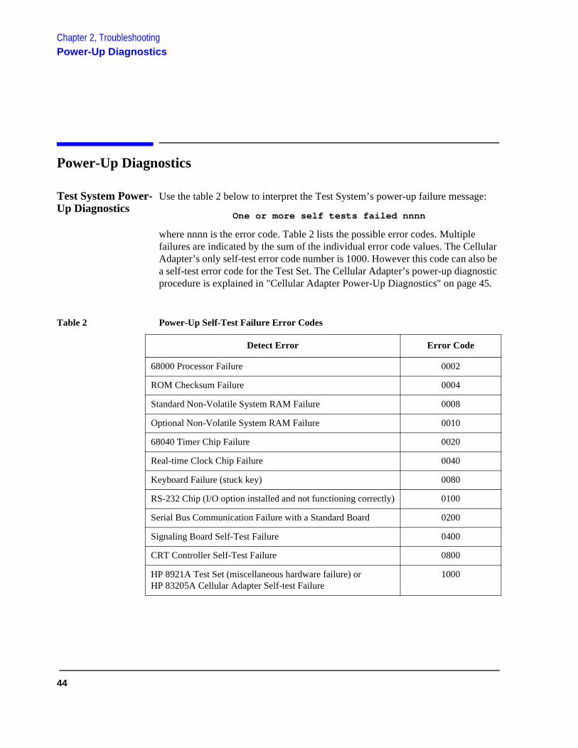
Test System Power-Up Diagnostics
Use the table 2 below to interpret the Test System’s power-up failure messag
One or more self tests failed nnnn
where nnnn is the error code. Table 2 lists the possible error codes. Multiple failures are indicated by the sum of the individual error code values. The CelAdapter’s only self-test error code number is 1000. However this code can alsa self-test error code for the Test Set. The Cellular Adapter’s power-up diagnprocedure is explained in "Cellular Adapter Power-Up Diagnostics" on page
Table 2 Power-Up Self-Test Failure Error Codes
Detect Error Error Code
68000 Processor Failure 0002
ROM Checksum Failure 0004
Standard Non-Volatile System RAM Failure 0008
Optional Non-Volatile System RAM Failure 0010
68040 Timer Chip Failure 0020
Real-time Clock Chip Failure 0040
Keyboard Failure (stuck key) 0080
RS-232 Chip (I/O option installed and not functioning correctly) 0100
Serial Bus Communication Failure with a Standard Board 0200
Signaling Board Self-Test Failure 0400
CRT Controller Self-Test Failure 0800
HP 8921A Test Set (miscellaneous hardware failure) or HP 83205A Cellular Adapter Self-test Failure
1000
44
Chapter 2, TroubleshootingPower-Up Diagnostics
ver.
en e
r off. el
Cellular Adapter Power-Up Diagnostics
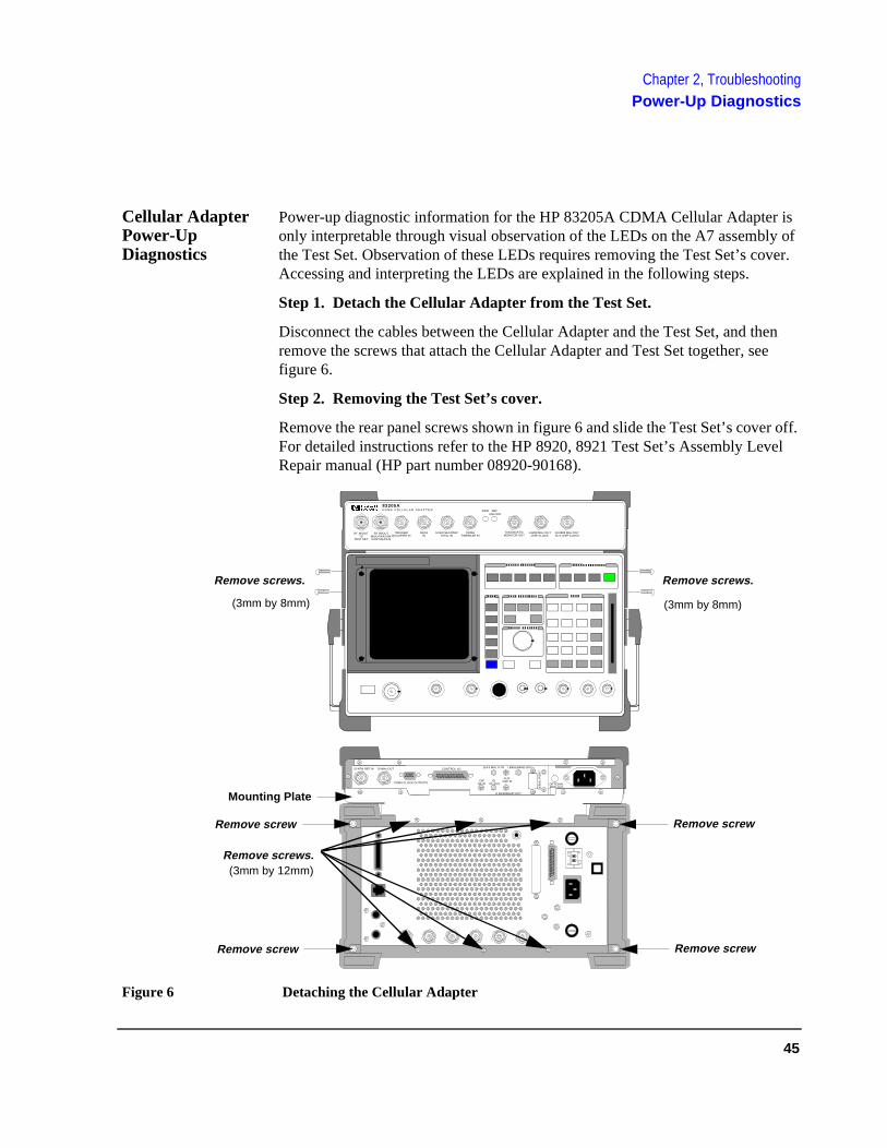
Power-up diagnostic information for the HP 83205A CDMA Cellular Adapter is only interpretable through visual observation of the LEDs on the A7 assembly of the Test Set. Observation of these LEDs requires removing the Test Set’s coAccessing and interpreting the LEDs are explained in the following steps.
Step 1. Detach the Cellular Adapter from the Test Set.
Disconnect the cables between the Cellular Adapter and the Test Set, and thremove the screws that attach the Cellular Adapter and Test Set together, sefigure 6.
Step 2. Removing the Test Set’s cover.
Remove the rear panel screws shown in figure 6 and slide the Test Set’s coveFor detailed instructions refer to the HP 8920, 8921 Test Set’s Assembly LevRepair manual (HP part number 08920-90168).
Figure 6 Detaching the Cellular Adapter
Remove screws.
(3mm by 8mm) (3mm by 8mm)
PWR REFUNLOCK
DIAGNOSTICMONITOR OUT
1.2288 MHz OUTCHIP CLOCK
19.6608 MHz OUT16 X CHIP CLOCK
RF IN/OUTTO
TEST SET
RF IN/OUTMAX.PWR 60WCONTINUOUS
83205AC D M A C E L L U L A R A D A P T E R
CDMATIMEBASE IN
EVEN SECOND/SYNC IN
DATAIN
TRIGGER/QUALIFIER IN
Remove screws.
114.3 MHz IF IN I BASEBAND OUT
AUXCW
RF INIQ
RF OUT OPTIONAL
SE
RIA
L P
OR
T
CONTROL I/OSYNTH REF IN 10 MHz OUT
CDMA CLOCK OUTPUTS DSP IN
MOD OUT
10 MHzREF OUT
Q BASEBAND OUT
Remove screws.
Mounting Plate
(3mm by 12mm)
Remove screw
Remove screw
Remove screw
Remove screw
45

Chapter 2, TroubleshootingPower-Up Diagnostics
Step 3. Reconnect the cabling between the Test Set and Cellular Adapter.
See figure 7 below.
Figure 7 Test Set and Cellular Adapter Cabling
MODULATIONINPUT
EXT SCOPETRIGGER INPUT
CRT VIDEOOUTPUT
10 MHz REFOUTPUT
10 MHz REFINPUT
AUDIO MONITOROUTPUT
DET OUT
IQRF IN
114.3 MHzIF
OUTCW RFOUT
HEADPHONE
AC FUSE
OP
TIO
N IN
TE
RF
AC
E
CO
NT
RO
L I/O
DC INPUT
PA
RA
LLE
L P
OR
T
HP
IB
(OP
TIO
N)
DC
C
UR
RE
NT
ME
AS
UR
EM
EN
T
+
-
SERIAL PORT
114.3 MHz IF IN I BASEBAND OUT
AUXCW
RF INIQ
RF OUT OPTIONAL
SE
RIA
L P
OR
T
CONTROL I/OSYNTH REF IN 10 MHz OUT
CDMA CLOCK OUTPUTSDSP IN
MOD OUT
10 MHzREF OUT
Q BASEBAND OUT
W6
W19
W17
W5
W4
W6
W17
HP 8921A Test Set Wire No. HP 83205A CDMA/CDPD Cellular Adapter
10 MHz REF OUT W1 SYNTH REF IN114.3 MHz IF OUT W2 114.3 MHz IF INDET OUT (DETECTOR) W3 AUX DSP INCW RF OUT W4 CW RF INIQ RF IN W5 IQ RF OUTCONTROL I/O W6 CONTROL I/OMODULATION INPUT W17* OPTIONAL MOD OUTSERIAL PORT, A1, B1, A0/B0 W19* SERIAL PORT
SERIAL PORT
SERIAL PORTA0/B0
SERIALPORT B1
SERIALPORT A1
* Options 002 & 003 only.
W2
W1W3
W2 W3
W1
W4 W5
46

Chapter 2, TroubleshootingPower-Up Diagnostics
Step 4. Power up the Test Set. Observe and record the patterns of the LEDs on the A7 assembly of the Test Set.
See figure 8.
Figure 8 Test Set LEDs
Step 5. Interpret the A7 LEDs of the Test Set.
During initial power-up, all the LEDs will light for approximately 10 seconds and then turn off. If a Cellular Adapter failure is detected after initial power-up, the first LED pattern (See figure 9 on page 48) will blink rapidly and represent a miscellaneous hardware pattern. The second and third LED patterns are non-blinking and represent failure details.
0123
A7 Assembly
HP 8921A Test Set
Front Back
LEDs
47

Chapter 2, TroubleshootingPower-Up Diagnostics
Figure 9 Hardware Failure Table
3 2 1 0
= off= rapid blink
= steady on or slow blink
LED Legend
3 2 1 0
3 2 1 0
3 2 1 0
if the last two non-blinking LED patterns displayed are ... ...then the failure is...
3 2 1 0 3 2 1 0
3 2 1 0
3 2 1 0
3 2 1 0
3 2 1 0
3 2 1 0 3 2 1 0
2nd LED Error Pattern 3rd LED Error Pattern
3 2 1 0
1st LED error pattern will blink rapidly and represent a miscellaneous failure...
the next two LED patterns are non-blinking and represent failure details...
HP 83205A’s (RX DSP) A2 assembly
Check firmware, see "Verifying Firmware Version" on page 88.
HP 83205A’s (Data Buffer) A5 assembly
Check firmware, see "Verifying Firmware Version" on page 88.
HP 83205A’s (RX DSP) A2 assembly
Replace this assembly.
HP 83205A’s (Data Buffer) A5 assembly
Replace this assembly.
48

Chapter 2, TroubleshootingVerifying Test Set Operation
lar r-
the
Verifying Test Set Operation
The Test Set must power up with no error messages and must run its functional diagnostics with no failures before you proceed with Cellular Adapter troubleshooting. Check this by disabling the Cellular Adapter, powering up the Test Set and then running the Test Set’s diagnostics (AF, RF, and MS).
Procedure Step 1. Disable the Cellular Adapter.
Disconnect all of the rear-panel cables that connect the Test Set to the CelluAdapter. Disconnect the Cellular Adapter’s power cord. On the Test Set’s reapanel, connect the IQ RF IN connector to the CW RF OUT connector.
Step 2. Switch ON the Test Set.
When the Test Set powers up, a self-test is run. If no problems are detected,message All self tests passed will be displayed. If an error code is displayed, you need to troubleshoot the Test Set before continuing with this procedure. Refer to the Test Set’s Assembly Level Repair manual (HP part number 08920-90168).
Step 3. Run the Test Set’s AF_DIAGS diagnostics.
a. Press the PRESET key.
b. Press the TESTS key.
c. Under Select Procedure Location: select ROM.
d. Under Select Procedure Filename: select AF_DIAGS.
e. Select the Run Test field.
f. Follow the instructions on the screen.
If all AF diagnostic tests pass, go on to the next step and run the RF diagnostics. If a test fails, repair the Test Set before continuing.
Step 4. Run the Test Set’s RF_DIAGS diagnostics.
a. Press the PRESET key.
b. Press the TESTS key.
c. Under Select Procedure Location: select ROM.
d. Under Select Procedure Filename: select RF_DIAGS.
e. Select the Run Test field.
49

Chapter 2, TroubleshootingVerifying Test Set Operation
n the
f. Follow the instructions on the screen.
If all RF and AF diagnostic tests pass, you can go to the next step and run MS diagnostics. If a test fails, repair the Test Set before continuing.
Step 5. Run the Test Set’s (Miscellaneous) MS_DIAGS diagnostics.
a. Press the PRESET key.
b. Press the TESTS key.
c. Under Select Procedure Location: select ROM
d. Under Select Procedure Filename: select MS_DIAGS.
e. Select the Run Test field.
f. Follow the instructions on the screen.
If all MS diagnostic tests pass, you can proceed with Cellular Adapter troubleshooting. If a test fails, repair the Test Set before continuing.
Step 6. Reconnect the Cellular Adapter.
Turn Off the Test Set and reconnect the Cellular Adapter’s cables as shown ifigure 7 on page 46. Reconnect the Cellular Adapter’s power cable.
50

Chapter 2, TroubleshootingVerifying that the Test Set Recognizes the Cellular Adapter
s the and
stem s lar
e
r" on , "Test
Verifying that the Test Set Recognizes the Cellular Adapter
Prerequisites Before performing the following procedure you must verify that the Test Set works and that the Test Set and the Cellular Adapter are connected correctly (see the previous procedure). The Cellular Adapter’s PWR LED must be on.
Procedure 1. Attempt to access the CDMA ANL screen.
Select the More field, and choose CDMA ANL from the list of displayed choices.
If the CDMA ANALYZER screen appears, the Test Set recognizes the Cellular Adapter. If not, continue with step 2 below.
2. Isolate the problem.
If the Test Set does not recognize the Cellular Adapter, the probable cause iA4 Gen/Ref Assembly. The A4 assembly has a serial I/O communication chipan EEPROM containing identification information. The Test Set’s controller reads the contents of the EEPROM over the serial I/O bus when the Test Sypowers up. If the serial I/O bus doesn’t work, the rest of the Cellular Adapter’power-up diagnostics will not run, and the Test Set will operate as if the CelluAdapter wasn’t there.
Before replacing the A4 assembly, it is a good idea to check the following:
• Check each pin of the CONTROL I/O cable for continuity. (Look for pins that havbeen damaged or pushed in.)
• Remove the Cellular Adapter’s cover (see "Separating Units and Removing Covepage 63) and check the power supply voltages on the A4 assembly. See figure 38System Power Distribution," on page 103.
51
Chapter 2, TroubleshootingCDMA Diagnostics
ter’s LD
et’s n
r the
m in r
CDMA Diagnostics
Prerequisites Before running the CDMA diagnostics (CDMA_DIAG), you must verify that the Test Set works and that it recognizes the Cellular Adapter. The Cellular AdapPWR LED must be on, the REF UNLOCK LED must be off, and the PER_CAcalibration procedure must have run without error.
Functional diagnostics to isolate Cellular Adapter failures reside in the Test SROM and are run from the TESTS screen. If diagnostics isolate a failure to aassembly, the screen indicates the possible faulty assembly along with the probability (high, medium, or low) of the diagnosis being correct.
CDMA_DIAG Procedure
To run the CDMA_DIAG program:
1. Press the PRESET key.
2. Press the TESTS key.
3. Set the Select Procedure Location: field to ROM. (See figure 10 on page 53).
4. Set the Select Procedure Filename: field to CDMA_DIAG.
5. Press Run Test (k1) key. The CDMA_DIAG screen appears, see figure 10 on page 53.
6. Follow the instructions on the screen.
If a test fails, notice which assembly is the likely cause by its probability facto(Low, Medium, or High). If more than one assembly is indicated, try replacingassemblies one at a time.
If the diagnostic tests intermittently fail, select the Loop (k1) function of the LOOPBACK TEST screen (see figure 10 on page 53) to place the Test Systea continuous test loop mode, then manually troubleshoot the Test System foloose connections.
52

Chapter 2, TroubleshootingCDMA Diagnostics
Figure 10 CDMA_DIAG Menu
1
Continue2
Help4
RF GENTo Screen
RF ANLAF ANL
TESTS (Main Menu)
LOAD TEST PROCEDURE:Select Procedure Locat ion:
Select Procedure Fi lename:
Description:
Library: Program:
CUSTOMIZE TEST PROCEDURE: SET UP TEST SET:
Channel Informat ionTest ParametersOrder of TestsPass/Fai l L imi tsSave/Delete Procedure
External DevicesPrinter Setup
IBASIC Cntr l
FreqParmSeqnSpecProc
CnfgPrint
Exec Execut ion Cond
IBASIC
Please select a procedure to load.
Choices:
RF_DIAGSMS_DIAGSDMC_DIAGLDMC_DIAGNCDMA_DIAGCDPD_DIAGEDNO_CALPER_CALPER_CALDRAM_MNG
ROM
Run Test
CDMA_DIAG
Select ROM as the location of the diagnostic program.Select the CDMA_DIAG diagnostic program.
Up
Down2
4
RF GENTo Screen
RF ANLAF ANLSCOPESPEC ANLENCODERDECODER
MORE
RADIO INT
TESTS (IBASIC Controller)
CDMA_DIAG INSTRUCTIONS: Position the menu pointerin front of the desired test using the Up and Downfields. Use the Select field to run the test.Use the Exit field to leave the program.
=>
3
Exit5
1
Loopback TestGen/Ref (A4), IQ Mod and LO/IF Module (A9)
CDMA_DIAG Menu
Select
Both of the following CDMA_DIAG Tests
Loop
2
4
RF GENTo Screen
RF ANLAF ANLSCOPESPEC ANLENCODERDECODER
MORE
RADIO INT
TESTS (IBASIC Controller)
3
Sgl Step5
1
Resume
Test#: Measured Parameter===========================1: RHO2: Frequency Error (Hz)3: Time Offset (uSec)4: Carrier Feedthru(dB)
LowerLimit=====.95
-100.00-5.00
-100.00
UpperLimit=====1.00
100.005.00
-20.00
ActualLimit=====1.00-.62.08
-59.29
LOOPBACK TEST
====================================================End of Loopback Test
===================================================
Stop Fail
Loopable function
Loopback Test Screen
53

Chapter 2, TroubleshootingCDMA Diagnostics
y.
e t in
The mbly es
plies, lection he st
CDMA_DIAG Tests Descriptions
The CDMA diagnostics can be run as loopable tests. This means that either a series of tests or an individual test can be set up to run repeatedly to aid in troubleshooting intermittent problems. (To do this, select all of the CDMA_DIAG tests from the menu after the program starts running, then press USER key (k1) (this selects the Loop function). Descriptions of the individual tests follow.
Loopback Test
If this test passes, it is very probable that the Cellular Adapter works correctly. A digital test pattern is generated, formatted, and timed in the A4 Gen/Ref assembly and then sent to the IQ Modulator in the A9 assembly. The test pattern modulates the RF carrier from the Test Set with Filtered Offset QPSK modulation.
The RF generator in the Test Set sets the level of the signal and loops it back to the RF analyzer where it is downconverted to 114.3 MHz and sent to Cellular Adapter’s LO/IF assembly in the A9 assembly. The LO/IF assembly downconverts the signal to 4.9 MHz and sends it to the A2 RX DSP assemblThe digital signal processor in the A2 assembly demodulates the signal and measures the CDMA waveform quality (rho), the RMS Error Vector Magnitud(EVM), amplitude error, frequency accuracy, and carrier feedthrough presenthe transmitted signal.
Gen/Ref (A4), IQ Mod and LO/IF Module (A9)
This test will help isolate a problem to the A4 assembly or the A9 assembly. A4 assembly is in the generator side of the Cellular Adapter and the A9 asseis in the analyzer side. The two are tested together because the test measursimilar parameters on each assembly.
These assemblies have multiplexers that select between grounds, power supVCO biases, tune-lines, detector voltages, and references, and routes the seto the front-panel DIAGNOSTIC MONITOR OUT connector. When this test isrun, the DIAGNOSTIC MONITOR OUT connector is connected externally to tTest Set’s AUDIO IN HI connector. The selection is then measured by the TeSet’s audio analyzer.
54

Chapter 2, TroubleshootingCDPD Diagnostics
CDPD Diagnostics
The diagnostic software, CDPD_DIAG, resides in the ROM of the Test Set. This software tests the CDPD function of the Cellular Adapter, Option 002 or 003. The CDPD_DIAG diagnostic program consists of three tests for testing the CDPD assembly and its connections. Before proceeding with the CDPD diagnostic tests, you must verify that the Test Set is operating correctly.
Figure 11 CDPD_DIAG Diagnostic Program
1
Continue2
Help4
RF GENTo Screen
RF ANLAF ANL
TESTS (Main Menu)
LOAD TEST PROCEDURE:Select Procedure Locat ion :
Se lect Procedure Fi lename:
Description:
Library: Program:
CUSTOMIZE TEST PROCEDURE: SET UP TEST SET:
Channel Informat ionTest ParametersOrder of TestsPass/Fa il L imitsSave/Delete Procedure
External DevicesPrinter Setup
IBASIC Cntr l
FreqParmSeqnSpecProc
CnfgPrint
Exec Execut ion Cond
IBASIC
Please select a procedure to load.
Choices:
AF_DIAGSRF_DIAGSMS_DIAGSDMC_DIAGLDMC_DIAGNCDMA_DIAGCDPD_DIAGEDNO_CALPER_CALPER_CALD
ROM
Run Test
CDPD_DIAG
Select ROM as the location of the diagnostic program.
Select the CDPD_DIAG diagnostic program.
CDPD_DIAG Menu
Begin Tst
2
4
RF GENTo Screen
RF ANLAF ANLSCOPESPEC ANLENCODERDECODER
MORE
RADIO INT
TESTS (IBASIC Controller)
CDPDDIAG INSTRUCTIONS: Position the menu pointerin front of the desired test using the Up and Downfields. Use the Begin Tst field to run the test.Use the Stop Tst field to leave this program.
=>
3
Stop Tst5
1
CDPD Module Self TestCDPD Digital Loop BackCDPD RF Loop Back
Down
Up
55
Chapter 2, TroubleshootingCDPD Diagnostics
CDPD_DIAG Procedure
See figure 11 on page 55 for an overview of this procedure. To access and perform the CDPD_DIAG diagnostic program:
1. Press the TESTS key. The TESTS (Main Menu) appears.
2. Select ROM for the procedure location, and then select CDPD_DIAG from the Choices: menu for the procedure filename.
3. Run the CDPD_DIAG program, press k1 (Run Test). The CDPD test options appear.
4. Select CDPD Module Self Test and then press k1 (Begin Tst).
Follow the instruction displayed. If an error message is encountered, see table 3 for the probable cause of failures. If a Tests Passed response is received, go to step 5.
5. Select Digital Loop Back, and then press k1 (Begin Tst).
Follow the instructions displayed. If an error message is encountered, see table 3 for the probable cause of failures. If a Valid response is displayed, go to step 6.
6. Select CDPD RF Loop Back, and then press k1 (Begin Tst).
Follow the instruction displayed. If an error message is encountered, see table 3 for the probable cause of failures. If a Valid response is received, this concludes testing.
56

Chapter 2, TroubleshootingCDPD Diagnostics
1. This table is based on the assumption that the diagnostic tests are performed in the order shown, that is, CDPD assembly Self Test first, CDPD Digital Loop Back test second, CDPD RF Loop Back test last.
2. If all else fails, call HP Factory Support for assistance, see "Factory Support" on page 35.
Table 3 CDPD Diagnostic Tests Error-Messages and Probable Causes
CDPD AssemblySelf Test 1
CDPD DigitalLoop Back Test
CDPD RF Loop Back Test
Probable Cause
No response or communication time out
Check serial communication path.
SRAM failure Failure in A11 CDPD assembly.
DSP failure Failure in A11 CDPD assembly.
Loopback failure Failure in A11 CDPD assembly.
Flash memory failure Failure in A11 CDPD assembly.
Synthesizer failure Failure in A11 CDPD assembly.
Test passed (PASS) Unable to put into digital loopback mode.
Cycle power to clear serial bus then try again.
Test passed (PASS) Unable to transmit. Failure in A11 CDPD assembly.
Test passed (PASS) Status NOT VALID. Failure in A11 CDPD assembly.
Test passed (PASS) PASS (status VALID) Unable to put into normal mode.
Cycle power to clear the serial bus then try again.
Test passed (PASS) PASS (status VALID) Unable to transmit. Failure in A11 CDPD assembly.
Test passed (PASS) PASS (status VALID) Unable to tune. Failure in A11 CDPD assembly.
Test passed (PASS) PASS (status VALID) Status NOT VALID. Faulty RF path in Cellular Adapter and Test Set, or failure in CDPD assembly. Refer to chapter 5, "Block Diagrams" on page 89 to aid you in understanding and isolating the problem.2
PASS PASS (status VALID) PASS (Status VALID) CDPD Tests successful.
57

Chapter 2, TroubleshootingCDPD Diagnostics
e
gram rt d
some n the ceived the ough
hat not user ure age
PD stem ent, ction
hat not user e on Loop
CDPD_DIAG Tests Descriptions
CDPD Module Self Test
The “CDPD Module Self Test” of the CDPD_DIAG menu verifies that the basCDPD hardware is operating correctly. This hardware includes the communication link between the Test Set and the CDPD assembly, CDPD processors, memory, synthesizer, and loopback hardware. The diagnostic prowill respond with “TESTS PASSED” or a failure message indicating which paof the diagnostic routine failed, see table 3 on page 57 for error messages anprobable causes.
CDPD Digital Loop Back
The digital loop back test goes one step further than the self test and verifies of the functions of the A11 CDPD assembly. This assembly is set to operate idigital loopback mode when three predefined messages are sent and then reand checked for a valid CDPD signal. This is all done in the digital portion of CDPD assembly. The RF circuits on the CDPD assembly and the RF path thrthe rest of the Test Set are not checked with this test.
If all three messages are successfully looped back, then the user is notified tCDPD status was VALID for all digital loops. If any one of these messages issuccessfully received or is corrupted, then the program stops and notifies thethat the CDPD status was NOT VALID for the digital loop back test, and a failmessage is displayed indicating which part of the test failed. See table 3 on p57 for error messages and probable causes.
RF Loop Back
The RF loop back test is similar to the digital loop back test except that the CDassembly is used in normal mode and the entire RF path through the Test Sy(Test Set and Cellular Adapter) is verified. Three predefined messages are sthen received, and checked for a valid CDPD signal. This test checks the funof the CDPD assembly and the RF path through the Test Set.
If all three messages are successfully looped back, then the user is notified tCDPD status was VALID for all digital loops. If any one of these messages issuccessfully received or is corrupted, then the program stops and notifies thethat the CDPD status was NOT VALID for the RF loop back test, and a failurmessage is displayed indicating which part of the RF loop failed. See table 3page 57 for error messages and probable causes. See figure 12, "CDPD RFBack Test Path," on page 59, for a diagram of the loop back test path.
58

Chapter 2, TroubleshootingCDPD Diagnostics
Figure 12 CDPD RF Loop Back Test Path
HP 83205A Cellular Adapter
DSP0.5 GMSK
CDPD Valid
AmplitudeControl
Directional Coupler
HP 8921A
DC FM
114.3 MHz
RF IN/OUT DUPLEX ANT INOUT
CDPD
MOD OUT
114.3 MHz IF OUT
114.3 MHz IF IN700 kHz
CW RF OUT
RCVR
IQIQ RF IN
IQ RF OUT
IBASIC
RJ11 DB15Serial Port
Serial Switch
CW RF IN
(SERIAL Cable)
RCVR
A9/A7
A9/A6
A10
A10
A11
A2
RX DSP
MOD IN
J4
J6
P3 J5
J6
J9
with CDPDTest Set
PWR REFUNLOCK
ANALYZER ANALYZER ANALYZER GENERATOR
83205AC D M A / C D P D C E L L U L A R A D A P T E R
RF IN/OUT
DUPLEX OUTRF IN/OUT
TO TEST SET
RF IN/OUT TO TEST SET
RF IN/OUT
RF IN/OUT
59

Chapter 2, TroubleshootingCDPD Diagnostics
60

3
Disassembly and Replacement
This chapter explains how to disassemble the HP 83205A CDMA/CDPD Cellular Adapter, Option 003, for the purpose of replacing failing assemblies. The following instructions are applicable to Options 001 and 002 of the Cellular Adapter. However, Option 001 will not have the CDPD assemblies and Option 002 will not have the (CDMA) A5 Data Buffer assembly.
61

Chapter 3, Disassembly and ReplacementDisassembly of the HP 83205A Cellular Adapter
.
e 66.
on
.
n
83.
Disassembly of the HP 83205A Cellular Adapter
Use table 4 below to help you access the main assemblies and sub components of the HP 83205A Cellular Adapter.
NOTE: This chapter shows the disassembly of the HP 83205A CDMA/CDPD Cellular Adapter Option 003. Options 001 and 002 are similar, however, Option 001 will not contain CDPD assemblies and Option 002 will not contain the (CDMA) A5 Data Buffer assembly.
1. To remove the A4 and A9 assemblies as one unit, see "Removing the A4 and A9 Assemblies as a Unit" onpage 76.
Table 4 HP83205A Cellular Adapter Disassembly Table
To... see...
remove the adapter’s cover... "Separating Units and Removing Cover" on page 63
operate the adapter without its cover... "Operation Without Cover" on page 65.
remove the A8 Power Supply assembly... "Removing the A8 Power Supply Assembly" on pag
remove the fuse holder, fan, or power supply cables... "Disconnecting Subassembly Power Connectors" page 67.
remove the front panel... "Removing the Front Panel" on page 68.
remove the rear panel... "Removing the Rear Panel" on page 70.
remove the A4 Generator/Reference assembly1... "Removing the A4 Gen/Ref Assembly" on page 72.
remove the A9 Reference/IQ assembly1... "Removing the A9 Reference/IQ Assembly" on page 74
remove the A4 and A9 assemblies as a unit... "Removing the A4 and A9 Assemblies as a Unit" opage 76.
remove the A10 Directional Coupler & Serial Switch assembly or semi-rigid cables...
"Removing the A10 Coupler & Switch Assembly and Semi-Rigid Cables" on page 78.
remove the A11 CDPD assembly... "Removing the A11 CDPD Assembly" on page 80.
remove the A2 RX DSP or A5 Data Buffer assembly... "Removing the A2 RX DSP and A5 Data Buffer Assemblies" on page 81.
remove the A3 Motherboard... "Removing the A3 Motherboard Assembly" on page
62
Chapter 3, Disassembly and ReplacementDisassembly of the HP 83205A Cellular Adapter
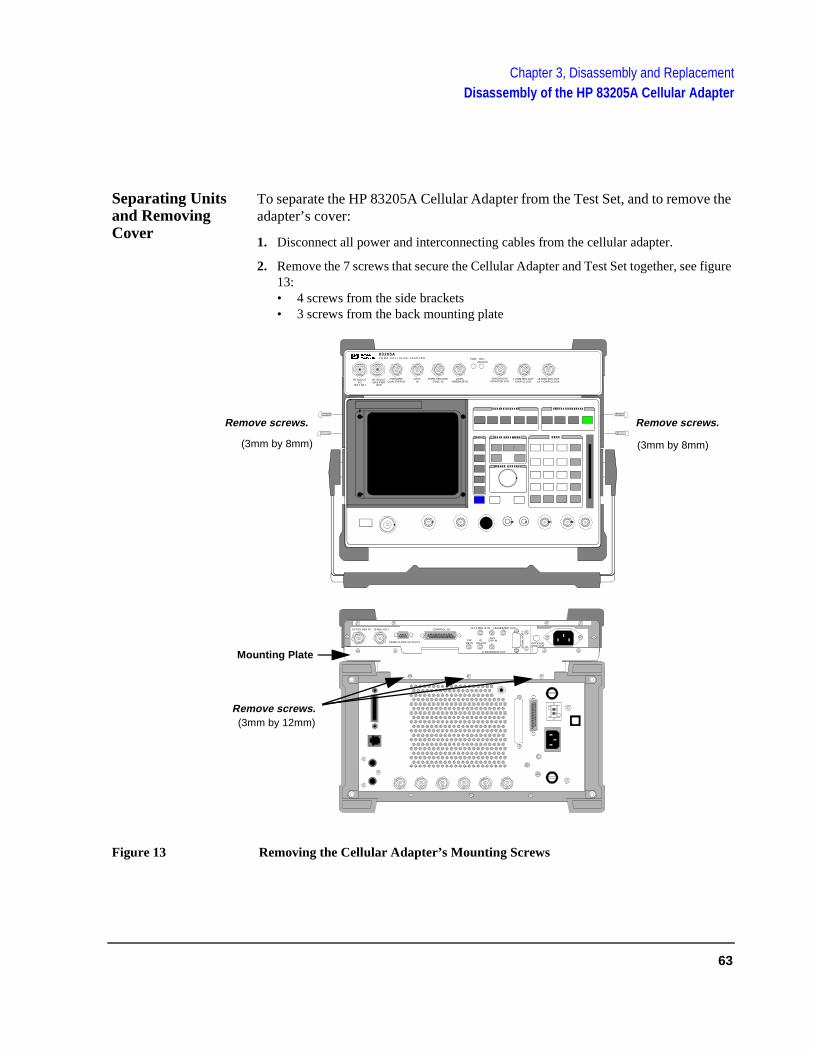
Separating Units and Removing Cover
To separate the HP 83205A Cellular Adapter from the Test Set, and to remove the adapter’s cover:
1. Disconnect all power and interconnecting cables from the cellular adapter.
2. Remove the 7 screws that secure the Cellular Adapter and Test Set together, see figure 13: • 4 screws from the side brackets • 3 screws from the back mounting plate
Figure 13 Removing the Cellular Adapter’s Mounting Screws
114.3 MHz IF IN I BASEBAND OUT
AUXCW
RF INIQ
RF OUT OPTIONAL
SE
RIA
L P
OR
T
CONTROL I/OSYNTH REF IN 10 MHz OUT
CDMA CLOCK OUTPUTS DSP IN
MOD OUT
10 MHzREF OUT
Q BASEBAND OUT
Remove screws.
Remove screws.
Mounting Plate
(3mm by 8mm) (3mm by 8mm)
(3mm by 12mm)
PWR REFUNLOCK
DIAGNOSTICMONITOR OUT
1.2288 MHz OUTCHIP CLOCK
19.6608 MHz OUT16 X CHIP CLOCK
RF IN/OUTTO
TEST SET
RF IN/OUTMAX.PWR
60W
83205AC D M A C E L L U L A R A D A P T E R
CDMATIMEBASE IN
EVEN SECOND/SYNC IN
DATAIN
TRIGGER/QUALIFIER IN
Remove screws.
63

Chapter 3, Disassembly and ReplacementDisassembly of the HP 83205A Cellular Adapter
3. Remove the cross bar and mounting plate from the adapter by removing the screws shown in figure 14.
4. Slide the cover from the adapter’s deck, see figure 15.
This concludes the procedure for removing the cover from the cellular adapter.
Figure 14 Removing the Cross Bar and Mounting Plate
Figure 15 Removing the Cover
114.3 MHz IF IN I BASEBAND OUT
AUXCW
RF IN
IQ
RF OUT OPTIONAL
SE
RIA
L P
OR
T
CONTROL I/OSYNTH REF IN 10 MHz OUT
CDMA CLOCK OUTPUTS
DSP IN
MOD OUT
10 MHzREF OUT
Q BASEBAND OUT
Remove screws.Remove screws.Cross Bar
Remove screws.
Mounting Plate
Remove screws.
All screws removed are 3mm by 12mm.
Top View
Cover (side view) Deck
64

Chapter 3, Disassembly and ReplacementDisassembly of the HP 83205A Cellular Adapter
Operation Without Cover
To operate the Cellular Adapter without its cover, place the Cellular Adapter on the Test Set without installing the screws that secure it to the Test Set, and then reconnect the rear panel cables as shown in figure 16.
Figure 16 Rear Panel Cable Connections for HP 83205A CDMA/CDPD Cellular Adapter
MODULATIONINPUT
EXT SCOPETRIGGER INPUT
CRT VIDEOOUTPUT
10 MHz REFOUTPUT
10 MHz REFINPUT
AUDIO MONITOROUTPUT
DET OUT
IQRF IN
114.3 MHzIF
OUTCW RFOUT
HEADPHONE
AC FUSE
OP
TIO
N IN
TE
RF
AC
E
CO
NT
RO
L I/O
DC INPUT
PA
RA
LLE
L P
OR
T
HP
IB
(OP
TIO
N)
DC
CU
RR
EN
T
ME
AS
UR
EM
EN
T
+
-
SERIAL PORT
114.3 MHz IF IN I BASEBAND OUT
AUXCW
RF INIQ
RF OUT OPTIONAL
SE
RIA
L P
OR
T
CONTROL I/OSYNTH REF IN 10 MHz OUT
CDMA CLOCK OUTPUTSDSP IN
MOD OUT
10 MHzREF OUT
Q BASEBAND OUT
W2W3
W1
W4 W5
W19
W17
W5
W2
W4
W3
W6
W1W17
HP 8921A Test Set Wire No. HP 83205A CDMA/CDPD Cellular Adapter
10 MHz REF OUT W1 SYNTH REF IN114.3 MHz IF OUT W2 114.3 MHz IF INDET OUT (DETECTOR) W3 AUX DSP INCW RF OUT W4 CW RF INIQ RF IN W5 IQ RF OUTCONTROL I/O W6 CONTROL I/OMODULATION INPUT W17* OPTIONAL MOD OUTSERIAL PORT, A1, B1, A0/B0 W19* SERIAL PORT
SERIAL PORT
SERIAL PORTA0/B0
SERIALPORT B1
SERIALPORT A1
* Options 002 & 003 only.
W6
65

Chapter 3, Disassembly and ReplacementDisassembly of the HP 83205A Cellular Adapter
Removing the A8 Power Supply Assembly
To remove the A8 power supply assembly:
1. Disconnect the output power connector to the A4 assembly, see figure 17.
2. Disconnect the primary power cable to the A8 assembly.
3. Remove 4 screws and lift the A8 power supply assembly from the deck.
This concludes the procedure for the removal of the A8 power supply assembly.
Figure 17 Removing the A8 Power Supply Assembly
Primary Power Cable
Output Power
A8 Power Supply
All screws removed are 3mm by 8mm.
Connector
66

Chapter 3, Disassembly and ReplacementDisassembly of the HP 83205A Cellular Adapter
Disconnecting Subassembly Power Connectors
Disconnect the connectors shown in table 5 and figure 18 if you need to replace the fan, fuse holder, A8 power supply assembly, or A3 motherboard.
Figure 18 Removing the Power Connectors
Table 5 Subassembly Connections
If replacing... Disconnect connector...
Fan (A4 assembly) J20 connector
Fuse holder (A3 assembly) J7 connector
Power supply assembly Primary and Output Power connectors (Also see "Removing the A8 Power Supply Assembly" on page 66.)
A3 motherboard (A3 assembly) J1 and J7 connectors
(A3) J7
(A4) J20
Rear Panel
Line Fuse Holder
Output Power Connector
A3 MotherboardA8 Power Supply Assembly
Fan
(A3) J1
Primary Power Connector
67
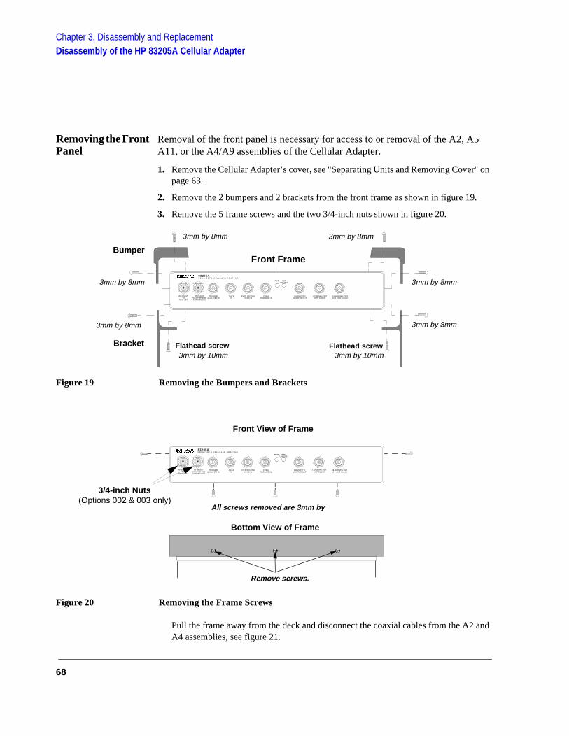
Chapter 3, Disassembly and ReplacementDisassembly of the HP 83205A Cellular Adapter
r" on
9.
and
Removing the Front Panel
Removal of the front panel is necessary for access to or removal of the A2, A5 A11, or the A4/A9 assemblies of the Cellular Adapter.
1. Remove the Cellular Adapter’s cover, see "Separating Units and Removing Covepage 63.
2. Remove the 2 bumpers and 2 brackets from the front frame as shown in figure 1
3. Remove the 5 frame screws and the two 3/4-inch nuts shown in figure 20.
Figure 19 Removing the Bumpers and Brackets
Figure 20 Removing the Frame Screws
Pull the frame away from the deck and disconnect the coaxial cables from the A2A4 assemblies, see figure 21.
PWR REFUNLOCK
83205AC D M A / C D P D C E L L U L A R A D A P T E R
RF IN/OUTTO
TEST SET
RF IN/OUTMAX.PWR 60WCONTINUOUS
Front FrameBumper
Bracket Flathead screw Flathead screw
DIAGNOSTICMONITOR OUT
1.2288 MHz OUTCHIP CLOCK
19.6608 MHz OUT16 X CHIP CLOCK
CDMATIMEBASE IN
EVEN SECOND/SYNC IN
DATAIN
TRIGGER/QUALIFIER IN
3mm by 8mm
3mm by 8mm
3mm by 8mm
3mm by 8mm
3mm by 8mm 3mm by 8mm
3mm by 10mm 3mm by 10mm
Bottom View of Frame
Front View of Frame
Remove screws.
All screws removed are 3mm by
PWR REFUNLOCK
83205AC D M A / C D P D C E L L U L A R A D A P T E R
RF IN/OUTTO
TEST SET
RF IN/OUTMAX.PWR 60WCONTINUOUS
DIAGNOSTICMONITOR OUT
1.2288 MHz OUTCHIP CLOCK
19.6608 MHz OUT16 X CHIP CLOCK
CDMATIMEBASE IN
EVEN SECOND/SYNC IN
DATAIN
TRIGGER/QUALIFIER IN
3/4-inch Nuts(Options 002 & 003 only)
68

Chapter 3, Disassembly and ReplacementDisassembly of the HP 83205A Cellular Adapter
Figure 21 Disconnecting the Coaxial Cables from the A4 and A5 Assemblies
This completes the procedure for removing the front panel. When reassembling the front panel frame, use table 6 below and figure 21 above to reconnect the cables of the front panel to the A4 assembly.
NOTE: When reinstalling the front cover, route the cables carefully to avoid crimping them.
A4 Assembly
Coaxial Cables
Deck
Frame
DIAGNOSTICMONITOR OUT
1.2288 MHz OUTCHIP CLOCK
19 6608 MHz OUT16 X CHIP CLOCK
A2 or A11 Assembly
EVEN SECOND/SYNC IN
CDMATIMEBASE IN
TRIGGER/QUALIFIER IN
DATA IN
J702J701
J703J1
J707J705
J706
J22 on A5 assembly(under A2 assembly)
(Top View)
5/8-inch Nuts(Options 002 & 003)
Table 6 Front Panel Connections
Connector/Cable of Front Panel goes to A4 or A5 connector...
TRIGGER/QUALIFIER IN (A4) J702
DATA IN (A5) J22
EVEN SECOND / SYNC IN (A4) J703
CDMA TIMEBASE IN (A4) J1
DIAGNOSTIC MONITOR OUT (A4) J707
1.2288 MHz OUT CHIP CLOCK (A4) J705
19.6608 MHz OUT 16 X CHIP CLOCK (A4) J706
69
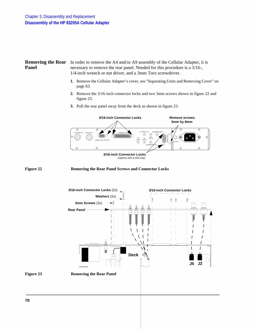
Chapter 3, Disassembly and ReplacementDisassembly of the HP 83205A Cellular Adapter
r" on
and
Removing the Rear Panel
In order to remove the A4 and/or A9 assembly of the Cellular Adapter, it is necessary to remove the rear panel. Needed for this procedure is a 3/16-, 1/4-inch wrench or nut driver, and a 3mm Torx screwdriver.
1. Remove the Cellular Adapter’s cover, see "Separating Units and Removing Covepage 63.
2. Remove the 3/16-inch connector locks and two 3mm screws shown in figure 22 figure 23.
3. Pull the rear panel away from the deck as shown in figure 23.
Figure 22 Removing the Rear Panel Screws and Connector Locks
Figure 23 Removing the Rear Panel
3/16-inch Connector Locks
114.3 MHz IF IN I BASEBAND OUT
AUXCW
RF INIQ
RF OUT
SE
RIA
L P
OR
T
CONTROL I/OSYNTH REF IN 10 MHz OUT
CDMA CLOCK OUTPUTSDSP IN
MOD OUT
10 MHzREF OUT
Q BASEBAND OUT
Remove screws.3mm by 8mm
3/16-inch Connector Locks(Options 002 & 003 only)
Deck
J5 J2
Rear Panel
3mm Screws (2x)
3/16-inch Connector Locks (2x)
Washers (2x)
3/16-inch Connector Locks
70

Chapter 3, Disassembly and ReplacementDisassembly of the HP 83205A Cellular Adapter
4. Access to other assemblies on the deck is now possible without removing the SMC connectors from the rear panel. If complete removal of the rear panel is necessary, use a 1/4-inch wrench or deep nut-driver to disconnect the SMC connectors and a 9/16-inch wrench to disconnect the BNC connectors, see figure 24.
Figure 24 Rear Panel Connector Removal
This completes the removal of the rear panel. Cable clips identify the location of the SMC connectors on the rear panel. When reinstalling the SMC and BNC connectors, use figure 22 and figure 23 on page 70 and table 7 below for identifying the location of the connectors.
0J3
0J71/4-inch Nut
Lock Washer
Rear Panel
Cable Clips
SMC Connector
9/16-inch Nut
Lock Washer
Rear Panel
BNC Connector
SMC Connector Removal BNC Connector Removal
0 J 3
Table 7 Rear Panel Connector Locations
Rear Panel Label Cable Clip Number (Connector Type)
114.3 MHz IF IN 0J1 (SMC)
AUX DSP IN 0J2 (SMC)
I BASEBAND OUT 0J3 (SMC)
CW RF IN 0J4 (SMC)
IQ RF OUT 0J5 (SMC)
Q BASEBAND OUT 0J6 (SMC)
SYNTH REF IN (BNC/cable goes to J2 on A4 assembly, see figure 23 on page 70.)
10 MHz OUT (BNC/cable goes to J5 on A4 assembly, see figure 23 on page 70.)
71

Chapter 3, Disassembly and ReplacementDisassembly of the HP 83205A Cellular Adapter
n
age
25 on
SMB ctor.
will ug it.
Removing the A4 Gen/Ref Assembly
The following instructions remove the A4 Generator/Reference assembly from the Cellular Adapter’s deck. An alternative to the following procedure is to remove the A4 and A9 assemblies as a unit, see "Removing the A4 and A9 Assemblies as a Unit" on page 76.
NOTE: Perform the "PER_CALD Calibration Procedure" on page 127 and "EBNO_CAL Calibration Procedure" on page 128 after replacing the A4 assembly.
To remove the A4 assembly:
1. Remove the Cellular Adapter’s cover, "Separating Units and Removing Cover" opage 63.
2. Remove the Cellular Adapter’s front panel, see "Removing the Front Panel" on p68.
3. Remove the rear panel, see "Removing the Rear Panel" on page 70.
4. Remove the 7 screws that secure the A4 assembly to the A9 assembly, see figurepage 73.
5. Disconnect from the A4 assembly: the fan, power, and ribbon cables, wires, and connectors shown in figure 25 on page 73. Cable clips identify each SMB conne
6. Carefully unplug the A4 assembly from the A3 motherboard’s J2 connector. You have to lift the opposite side of the A4 assembly over the edge of the deck to unpl
This completes the removal of the A4 assembly. Use figure 25 on page 73 to identify the location of the connectors and cables when reinstalling the A4 assembly.
72

Chapter 3, Disassembly and ReplacementDisassembly of the HP 83205A Cellular Adapter
Figure 25 Removing the A4 Assembly
A9 Assembly
J11
SMB Connector
Fan Connector
All screws removed are 3mm by 8mm.
J400J500
J708J401
J7
J9
J10
A4 Assembly
J20J5
J2
J3
J709
J11
(4J11-10J2)W22
W23W7(A4J5-[RP]10 MHz OUT)
(A4J2-[RP] SYNTH REF IN)
A1W7
A3J2 Connector
A1W6
A1W4 A1W5
A1W3 W9
A1W1
W16
(A8W1)(A12B1)
W34
J20 J9
(J10)J709 J4
W33 W32
W31
W30
W29(4J400-5J401)
(4J500-5J501) (4J708-5J4)
(4J401-7J5)
(4J3-6J2)
(4J7-2J4)
W28
Assembly A7, Connector J5
to Assembly A4, Connector J3
(7J5-4J3)Wirereferencedesignator
Cable Legend
J702J701
J703J1
J707J705
J706
W22(4J11-10J2)
A1W7 (4J706- [FP]19.6608 MHz OUT)
A1W6 (4J705- [FP] 1.2288 MHz OUT CHIP CLOCK)
A1W4 (4J1- [FP] CDMA TIMEBASE IN)A1W5 (4J707- [FP] DIAGNOSTIC MONITOR OUT)
A1W3 (4J703-[FP] EVEN SECOND/SYNC IN)W9 (4J701-5J709)
A1W1 (4J702-[FP] TRIGGER/QUALIFIER IN)
Power Cable
Ribbon Cable
[RP] = Rear Panel[FP] = Front Panel
73
Chapter 3, Disassembly and ReplacementDisassembly of the HP 83205A Cellular Adapter
ine
Removing the A9 Reference/IQ Assembly
The following instructions remove the A9 Reference/IQ assembly unit from the Cellular Adapter’s deck. An alternative to this procedure is to remove the A4assembly and the A9 assembly as a unit, see "Removing the A4 and A9 Assemblies as a Unit" on page 76.
NOTE: Perform the "PER_CALD Calibration Procedure" on page 127 and "EBNO_CAL Calibration Procedure" on page 128 after replacing the A4 assembly.
1. Remove the cover from the Cellular Adapter. See "Separating Units and Removing Cover" on page 63.
2. Remove the front panel. See "Removing the Front Panel" on page 68.
3. Remove the rear panel. See "Removing the Rear Panel" on page 70.
4. Remove the A4 Gen/Ref assembly. See "Removing the A4 Gen/Ref Assembly" on page 72.
5. Remove the 6 screws that secure the A9 assembly to the deck, see figure 26 on page 75, and carefully lift the assembly from the deck.
6. Disconnect the SMB connectors from the A9 assembly, see figure 26. The SMB cables are identified with cable clips.
This completes the removal and disassembly of the A9 assembly unit. Whenreassembling the A9 assembly, use figure 26 on page 75 to help you determthe location of the SMB coaxial cables which are identified with cable clips.
74

Chapter 3, Disassembly and ReplacementDisassembly of the HP 83205A Cellular Adapter
Figure 26 Removing the A9 Reference/IQ Assembly
A9 Assembly
All screws removed are 3mm by 30mm.
W37W24
W30
A6 SubassemblyA7 Subassembly
A9 Assembly
W27W35
W28
W31
Ribbon Cable (W16)
(6J2-4J3)
W20(6J6-11J3) (6J3-[RP]OJ1) (6J4-2J6)
(7J5-4J401)
(7J4-[RP]OJ5)
W36(7J3-5J400)
W21(7J6-11J4)
(7J2-5J500)(7J1-[RP]OJ4)
SMB Coaxial Cable
W28
Assembly A7, Connector J5
to Assembly A4, Connector J3
(7J5-4J3)Wirereferencedesignator
Cable Legend
[RP] = Rear Panel[FP] = Front Panel
75

Chapter 3, Disassembly and ReplacementDisassembly of the HP 83205A Cellular Adapter
Removing the A4 and A9 Assemblies as a Unit
The following instructions remove the A4 Generator/Reference assembly and A9 Reference/IQ assembly as a unit from the Cellular Adapter’s deck.
NOTE: Perform the "PER_CALD Calibration Procedure" on page 127 and "EBNO_CALCalibration Procedure" on page 128 after replacing the A4 assembly.
1. Remove the cover from the Cellular Adapter. See "Separating Units and Removing Cover" on page 63.
2. Remove the front panel. See "Removing the Front Panel" on page 68.
3. Remove the rear panel. See "Removing the Rear Panel" on page 70.
4. Remove the 6 screws that secure the A4 and A9 assemblies to the deck, see figure 27 on page 77.
5. Carefully pull the A4/A9 assembly away from theA3 motherboard and lift it over the edge of the deck to disconnect the cables and connectors shown in figure 27 on page 77.
This completes the removal of the A4/A9 assembly unit.
Reinstalling the A4/A9 Assembly
To reinstall the A4/A9 assembly, reverse the steps of the previous section.
1. Reconnect the SMB connectors to their proper assemblies. Use figure 27 on page 77 to help you determine the location of the cables and SMB coaxial connectors. The ends of the coaxial cables are identified with cable clips.
2. Carefully plug the A4/A9 assembly into the A3 motherboard. Ensure that the assembly is squarely plugged in and be sure not to get a cable caught under the A4/A9 assembly or you will have difficulty trying to fasten down the assembly.
3. Secure the assembly with the 6 screws (3mm by 30mm) previously removed.
4. Reconnect all remaining cables and connectors to their proper assemblies as shown in figure 27 on page 77.
5. Reinstall the back and front panels.
This concludes the procedure for reinstalling the A4/A9 assemblies.
76

Chapter 3, Disassembly and ReplacementDisassembly of the HP 83205A Cellular Adapter
Figure 27 Removing the A4/A9 Assembly as a Unit
All screws removed are 3mm by 30mm.
A4 & A9 Assembly
Power Cable
W22
W37W24W30
A6 SubassemblyA7 Subassembly
A9 Assembly
W27
W35
W36
W28
W31
W21SMB Coaxial Cables
J1
Ribbon Cable (W16)
J9J20
W30W31
W32
A4 AssemblyW29
J9
A1W7A1W6
A1W4 A1W5
J11
A1W7 (4J706- [FP]19.6608 MHz OUT)
A1W6 (4J705- [FP] 1.2288 MHz OUT CHIP CLOCK)
A1W4 (4J1- [FP] CDMA TIMEBASE IN)A1W5 (4J707- [FP] DIAGNOSTIC MONITOR OUT)
A1W3 (4J703-[FP] EVEN SECOND/SYNC IN)W9 (4J701-5J709)
A1W1 (4J702-[FP] TRIGGER/QUALIFIER IN)
(4J11-10J2)
A1W3 W9
A1W1
(7J5-4J401)
(7J4-[RP]OJ5)
(7J3-5J400)
(7J6-11J4)
(7J2-5J500)
(7J1-[RP]OJ4)(6J2-4J3)
W20(6J6-11J3) (6J4-2J6)(6J3-[RP]OJ1)
J5J2
W23
W7(A4J5-[RP]10 MHz OUT)
(A4J2-[RP] SYNTH REF IN)
Fan Cable
W34(4J400-5J401)
(4J500-5J501)W33
(4J708-5J4)(4J7-2J4)(4J3-6J2)
(4J401-7J5)
(4J11-10J2)W22
J10
J702J701
J703J1
J707J705
J706
W28
Assembly A7, Connector J5
to Assembly A4, Connector J3
(7J5-4J3)Wirereferencedesignator
Cable Legend
[RP] = Rear Panel[FP] = Front Panel
77
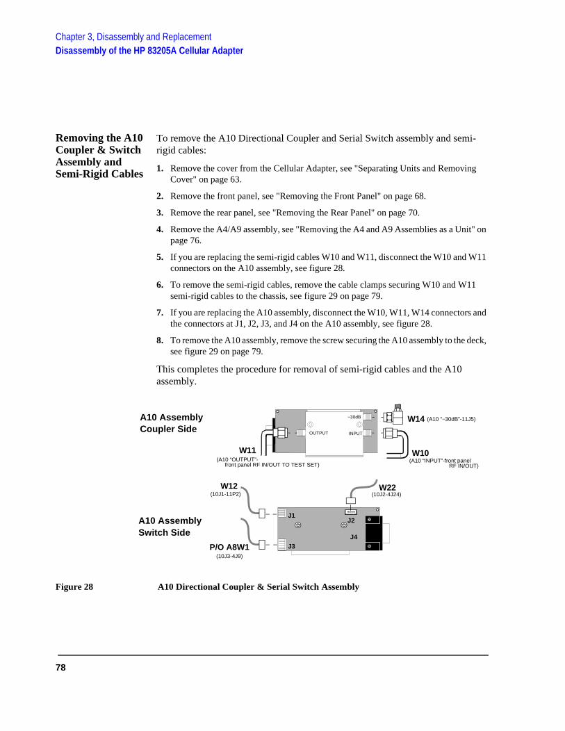
Chapter 3, Disassembly and ReplacementDisassembly of the HP 83205A Cellular Adapter
Removing the A10 Coupler & Switch Assembly and Semi-Rigid Cables
To remove the A10 Directional Coupler and Serial Switch assembly and semi-rigid cables:
1. Remove the cover from the Cellular Adapter, see "Separating Units and Removing Cover" on page 63.
2. Remove the front panel, see "Removing the Front Panel" on page 68.
3. Remove the rear panel, see "Removing the Rear Panel" on page 70.
4. Remove the A4/A9 assembly, see "Removing the A4 and A9 Assemblies as a Unit" on page 76.
5. If you are replacing the semi-rigid cables W10 and W11, disconnect the W10 and W11 connectors on the A10 assembly, see figure 28.
6. To remove the semi-rigid cables, remove the cable clamps securing W10 and W11 semi-rigid cables to the chassis, see figure 29 on page 79.
7. If you are replacing the A10 assembly, disconnect the W10, W11, W14 connectors and the connectors at J1, J2, J3, and J4 on the A10 assembly, see figure 28.
8. To remove the A10 assembly, remove the screw securing the A10 assembly to the deck, see figure 29 on page 79.
This completes the procedure for removal of semi-rigid cables and the A10 assembly.
Figure 28 A10 Directional Coupler & Serial Switch Assembly
J1J2
J4J3
A10 Assembly
A10 Assembly
W10
W14
W11
Coupler Side
W12(10J1-11P2)
P/O A8W1
(10J2-4J24)W22
Switch Side
OUTPUT INPUT
−30dB (A10 “−30dB”-11J5)
(A10 “INPUT”-front panelRF IN/OUT)
(A10 “OUTPUT”-front panel RF IN/OUT TO TEST SET)
(10J3-4J9)
78

Chapter 3, Disassembly and ReplacementDisassembly of the HP 83205A Cellular Adapter
Figure 29 Removing the A10 Directional Coupler & Serial Switch Assembly & Semi-Rigid Cables
A10 Assembly
Screws removedare 3mm by 6mm.
W10 (Semi-rigid cable)
W11 (Semi-rigid cable)
Cable Clamp
Directional Coupler
W14& Serial Switch
79

Chapter 3, Disassembly and ReplacementDisassembly of the HP 83205A Cellular Adapter
Removing the A11 CDPD Assembly
If the Cellular Adapter is an Option 001 (CDMA only), the following instructions do not apply since it does not contain the A11 CDPD assembly.
To remove the A11 CDPD assembly in Option 002 or 003:
1. Remove the cover from the Cellular Adapter, see "Separating Units and Removing Cover" on page 63.
2. Remove the front panel, see "Removing the Front Panel" on page 68.
3. Remove the 4 machine screws securing the A11 assembly, see figure 30.
4. Disconnect the cables and connectors shown in figure 30 from the A11 assembly.
5. Carefully lift the A11 assembly over the edge of the Cellular Adapter and pull it away from the A3 motherboard.
This completes the procedure for the removal of the A11 assembly.
Figure 30 Removing the A11 CDPD Assembly
W12 (11P2-10J1)
W13 (11P3-2J9)
A8W1-11J2
A11 Assembly
MP11
W21 (11J4-7J6)
W20 (11J3-6J6)
W15 (11J6-OPTIONAL
W14 (11J5-A10 “INPUT”)
A2J9P3
P2
J2
MODE OUT)
W28
Assembly A7, Connector J5
to Assembly A4, Connector J3
(7J5-4J3)Wirereferencedesignator
Cable Legend
[RP] = Rear Panel[FP] = Front Panel
80

Chapter 3, Disassembly and ReplacementDisassembly of the HP 83205A Cellular Adapter
Removing the A2 RX DSP and A5 Data Buffer Assemblies
To replace the A2 RX DSP or A5 Data Buffer assembly:
1. Remove the cover from the Cellular Adapter, see "Separating Units and Removing Cover" on page 63.
2. Remove the front panel of the cellular adapter. See "Removing the Front Panel" on page 68.
3. If the Cellular Adapter is an Option 002 or 003, remove the A11 CDPD assembly, see see "Removing the A11 CDPD Assembly" on page 80.
4. If the Cellular Adapter is an Option 001, remove the 2 screws securing the A2 assem-bly, see figure 31.
5. Disconnect the cables and SMB connectors shown in figure 31 from the A2 assembly.
Figure 31 Removing A2 RX DSP Assembly
6. With a flat blade screwdriver wedged between the A2 assembly and the A3 mother-board assembly, carefully push and tilt the end of the A2 assembly over the edge of the deck to unplug it from the J3 and J4 connectors of the motherboard, see figure 31.
A2 Assembly
W29
W37
A5 AssemblyA2
W25
Screws
W13
(Option 001 only)
(2J6-6J4)
(2J4-4J7)
(2J9-11P3)
(2J3-[RP]OJ2)
A3J3
A3J4
A3 Assembly
81

Chapter 3, Disassembly and ReplacementDisassembly of the HP 83205A Cellular Adapter
7. To remove the A5 Data Buffer assembly, disconnect the cables and connectors shown in figure 32 from the A5 assembly.
8. Using the flat-blade screwdriver, carefully pry and tilt the end of the A5 assembly over the edge of the deck and unplug it from the J5 and J6 connectors of the A3 assembly, see figure 32.
This completes removal of the A2 and A5 assemblies. When reinstalling the A2 and A5 assemblies, use figure 31 on page 81 and figure 32 to identify the location of the cables and connectors.
Figure 32 Removing the A5 Data Buffer Assembly
A5 Assembly
W9
W32(J709)
(J22)
A1W2
(5J4-4J708)
(4J701-5J709)
(5J22 - front panel DATA IN.)A5
W8
W35 W33W34 W36
W26(5J502-[RP]OJ6)
(5J500-7J2)(5J501-4J500)
(5J401-4J400)(5J400-7J3)
(5J402-[RP]OJ3)
A3 Assembly
82

Chapter 3, Disassembly and ReplacementDisassembly of the HP 83205A Cellular Adapter
Removing the A3 Motherboard Assembly
The following procedure removes and disassembles the A3 motherboard assembly.
1. Remove the cover from the Cellular Adapter, see "Separating Units and Removing Cover" on page 63.
2. Remove the front panel, see "Removing the Front Panel" on page 68.
3. Remove the rear panel, see "Removing the Rear Panel" on page 70.
4. Remove the A4 assembly, see "Removing the A4 Gen/Ref Assembly" on page 72.
5. Remove the A9 assembly, see "Removing the A9 Reference/IQ Assembly" on page 74.
6. If the Cellular Adapter is an option 002 or 003, remove the A11 assembly, see "Remov-ing the A11 CDPD Assembly" on page 80.
7. Remove the A2 and A5 assemblies, see "Removing the A2 RX DSP and A5 Data Buff-er Assemblies" on page 81.
8. Remove the power connectors from the J7 and J1 connectors on the A3 assembly, see figure 33.
9. If the Cellular Adapter is an Option 001, remove the 4 screws securing the A3 assembly to the deck, see figure 33. If the Cellular Adapter is an Option 002 or 003, two of the screws secure the CDPD semi-rigid cables to the deck, see figure 29 on page 79.
This completes the procedure for the removal of the A3 assembly. To reassemble the Cellular Adapter, follow the previous steps in reverse order.
Figure 33 Removing the A3 Motherboard Assembly
J7
J1
A3 Assembly
Screws removed are 3mm by 6mm.
83

Chapter 3, Disassembly and ReplacementDisassembly of the HP 83205A Cellular Adapter
84

4
Modifications
This chapter explains how to load and verify firmware upgrades on the HP 83205A Cellular Adapter.
85

Chapter 4, ModificationsFirmware Upgrades
e ts n
Firmware Upgrades
Firmware in the HP 83205A Cellular Adapter and its companion HP 8921A Cell Site Test Set should be upgraded to the latest revision any time a repair is made or a performance problem is discovered.
The Test Set’s firmware is upgraded by installing new PROMs. These are available by ordering the HP 8921A Test Set firmware upgrade kit (HP 8921A R98).
The Cellular Adapter’s firmware is upgraded by running a program that downloads the new firmware files from a memory card and stores them in thEEPROM’s on the A2 RX DSP assembly. Table 8 below lists the upgrade kiavailable. For ordering information, see "Service Information," in chapter 1, opage 35.
Table 8 Firmware Upgrade Kits
Kit Description
83205-61801 HP 83205A Cellular Adapter firmware
HP 8921A R98 HP 8921A Test Set firmware
83204-61807 CDPD application software
HP 83205A R99 All of the above.
86

Chapter 4, ModificationsFirmware Loading and Verification
et’sand
if
hen
Firmware Loading and Verification
NOTE: The DSP firmware download program in the following section checks the Test Sfirmware revision for compatibility. If the Test Set’s firmware is not compatible, order install the latest firmware revision. Order kit HP 8921A R98. For ordering information,see "Service Information," in chapter 1, on page 35.
Load the DSP Firmware
The following procedure loads the Digital Signal Processor firmware.
1. Press the PRESET key.
2. Insert the 83205-10001 memory card into the Test Set.
3. Press the TESTS key.
4. Set the Select Procedure Location: field to Card.
5. Set the Select Procedure Filename field to DLFIRM.
6. Select Run Test (k1) key.
7. Follow the instructions on the screen.
After the firmware is downloaded, be sure to cycle the Test System’s power you are not loading CDPD firmware, otherwise, see the following procedure.
Load the CDPD Firmware
The following procedure loads the CDPD firmware.
1. Press the PRESET key.
2. Insert the 83205-10004 memory card into the Test Set.
3. Press the TESTS key.
4. Set the Select Procedure Location: field to Card.
5. Set the Select Procedure Filename field to CDPDULD.
6. Select Run Test (k1) key.
7. Follow the instructions on the screen.
After the firmware is downloaded, be sure to cycle the Test System’s power wcomplete.
87

Chapter 4, ModificationsFirmware Loading and Verification
ion
on
t’s
page
en
Verifying Firmware Version
The following procedure checks the current version of the firmware in the HP 8921A Test Set and the Cellular Adapter.
1. Power on the Test System.
2. Check the firmware level of the Test Set, the firmware level appears in the upper part of the RX TEST screen:
• For the HP 83205A CDMA Cellular Adapter (Option 001), the Test Set’s verslevel must be A.16.00 or higher.
• For the HP 83205A CDPD Cellular Adapter (Option 002), the Test Set’s versilevel must be A.17.00 or higher.
• For the HP 83205A CDMA/CDPD Cellular Adapter (Option 003), the Test Seversion level must be A.17.00 or higher.
If the Test Set does not have the proper firmware, see "Firmware Upgrades" on 86 for ordering an upgrade kit.
3. Press the blue SHIFT key, then the DUPLEX (CONFIG) key. The Configure screappears.
4. Select SERVICE from the To Screen menu. The Service screen appears.
5. Select the Latch field.
6. Move the cursor to rx_dsp_revision under the Choices: menu and press theknob.
7. Read the RX DSP firmware version from the Value field. The value is actually a datein the form YYYYMMDD (Y=year, M=month, D=day).
Compare this date to the date on the new DSP firmware memory card.
88

5
Block Diagrams
This chapter provides information for helping you understand the operation of the HP 83205A Cellular Adapter and its CDMA and CDPD options.
89

Chapter 5, Block DiagramsInstrument Description
gh e
ates
he old
t tation, is cket
Instrument Description
The HP 83205A Cellular Adapter is an add-on-instrument for the HP 8921A Test Set. The Cellular Adapter is controlled by the Test Set’s host processor throuthe Test Set’s front-panel selections or HP-IB commands to the Test Set. ThCellular Adapter mounts on top of the Test Set.
Adding the CDMA Cellular Adapter, Options 001 and 003, to the Test Set crea system for testing cellular base stations to the CDMA standard. The CDMAstandard uses digital compression to increase the number of channels over tAMPS system.
The CDPD Cellular Adapters, Options 002 and 003, include Cellular Digital Packet Data (CDPD) digital signal generation and analysis. CDPD is a packedata system which overlays the existing AMPS voice system, is designed forsending packet data, and uses a separate base station (Mobile Data Base SMDBS) which is integrated into the antenna system of a cell site. When thereno voice traffic on a designated AMPS voice channel, the MDBS transmits padata to mobile end stations or fixed end stations. When AMPS voice traffic isassigned to that channel, the MDBS must power down and reacquire communications on another designated CDPD channel if available.
90

Chapter 5, Block DiagramsCDMA Cellular Adapter
es
apter.
CDMA Cellular Adapter
Options 001 and 003 of the HP 83205A Cellular Adapter contain CDMA digital signal processing hardware and firmware to test the transmitter and receiver portions of CDMA base stations.
The Test Set’s CDMA Generator and CDMA ANL test screens have fields for controlling the Cellular Adapter and for displaying measurement results. TheCONTROL I/O cable (not shown on the simplified block diagram below) passthe digital control and data signals between the Test Set and the Cellular Ad
Figure 34 CDMA Test System Overview
CDMA Cellular AdapterHP 8921A Test Set
Reference 10 MHz
Downconverter to IF
RF IN/OUT
DUPLEX OUT
REF IN
114.3 IF OUT
114.3 MHz IF IN
3.6864 MHz
CW RF OUT
IQIQ RF IN IQ RF OUT
CW RF INA7
A6
A5 Data Buffer
A2 RX DSP
RX DSP
10 MHz
Radio Under Test
ANT
I/Q Mod
Ref/RX
ANT IN
A9
REF OUTPUT
A4 Gen/Ref
CW Source
PLL
Clock & Sampling Signals
SYNTH
91

Chapter 5, Block DiagramsCDMA Cellular Adapter
CDMA Analysis
The CDMA signal is down converted to 114.3 MHz IF by the Test Set before being passed to the Cellular Adapter. The LO/IF (A6) downconverts the 114.3 MHz IF to a 3.6864 MHz IF before passing the signal on to the A2 Receiver DSP assembly for processing, see figure 34 on page 91.
CDMA Generation
The A5 Data Buffer assembly generates data that emulates a CDMA traffic channel and provides a calibrated noise source. The Generator/Reference then converts the data into I and Q drive signals. The signal is then passed to the I/Q Modulation (A7 assembly) where it is modulated with the RF from the Test Set. The signal is then passed to the Test Set for amplification.
92
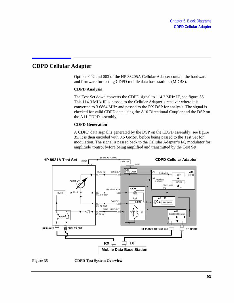
Chapter 5, Block DiagramsCDPD Cellular Adapter
l is on
gure r r for
CDPD Cellular Adapter
Options 002 and 003 of the HP 83205A Cellular Adapter contain the hardware and firmware for testing CDPD mobile data base stations (MDBS).
CDPD Analysis
The Test Set down converts the CDPD signal to 114.3 MHz IF, see figure 35. This 114.3 MHz IF is passed to the Cellular Adapter’s receiver where it is converted to 3.6864 MHz and passed to the RX DSP for analysis. The signachecked for valid CDPD data using the A10 Directional Coupler and the DSPthe A11 CDPD assembly.
CDPD Generation
A CDPD data signal is generated by the DSP on the CDPD assembly, see fi35. It is then encoded with 0.5 GMSK before being passed to the Test Set fomodulation. The signal is passed back to the Cellular Adapter’s I/Q modulatoamplitude control before being amplified and transmitted by the Test Set.
Figure 35 CDPD Test System Overview
CDPD Cellular Adapter
DSP0.5 GMSK
CDPD Valid
AmplitudeControl
Directional Coupler
HP 8921A Test Set
DC FM
114.3
RF IN/OUT DUPLEX OUT
CDPDMOD OUT
114.3 IF OUT
114.3 MHz IF IN3.6864 MHz
CW RF OUT
RCVR
IQIQ RF IN
SYNTH IQ RF OUT
IBASIC
RJ DB15Serial Port
Serial Switch
CW RF IN
(SERIAL Cable)
RCVR
A9/A7
A9/A6
A10
A10
A11
A2
RX DSP
MOD IN
J4
J6
P3 J5
J6
J9
Mobile Data Base Station
TXRX
RF IN/OUTRF IN/OUT TO TEST SET
93

Chapter 5, Block DiagramsAssembly Descriptions
Assembly Descriptions
Table 9 describes the major assemblies and subassemblies that make up the Cellular Adapter. Use the diagram shown in figure 36 on page 95 for a visual overview of the Test System.
Table 9 Quick Reference of Assemblies
AssemblyDesignator
Assembly Name Function
A2 Receiver DSP (Digital Signal Processor) Data analyzer
A4 Generator/Reference Encodes the I/Q channels
A5 Data Buffer Data generator
A9 Reference/IQ Houses the A6 & A7 assemblies
A9/A6 LO/IF Receiver and down converter
A9/A7 IQ Modulator Modulates the RF carrier with π/4 DQPSK
A10 CDPD Directional Coupler & Serial Switch
The directional coupler couples the CDPD signal for verification. The serial switch switches Test Set communication between the premod filter and the CDPD assembly.
A11 CDPD module Provides CDPD protocol processing
94

Chapter 5, Block DiagramsAssembly Descriptions
114.3 IF IN (
IQ
CWIN (
Hz (RP)
IGGER/ALIFIER
RF O(RP
T
(RP)
I Out(RP)
Q Out(RP)
NTHEFPUTP)
CO
PS
OPTIMOD
Figure 36 Test System Block Diagram
A9 Ref/ IQMHzRP)
A6 LO/IF
A7 I/Q Modulator
A2 RX DSP128K FLASH
EPROM256K
Fast RAM 33 MHz
THS320C30DSP
ADDRDecode
12 BITADC
8 MHz
-10 to +30 dB
RFRP)
I Q ModAssembly
1 GHz
RF InRF Out
I Drive Q Drive
10
DIAG
DIAGNOSTICA4 Gen/Ref Board
DATA IN
EVEN SEC/
GDATA
DataBuffer
ParallelTo
SerialInterface
CONTROL
U1
÷N
Σ
10MOUT
TRQU
HostInter-
DataLatch
DIAG 0DIAG 1
DIAG 2DIAG 3
DE-MUX12 TO 24
TrigCircuit
SampleClock
Generator
MUX
Quad Adjust
PWR+12V, +12VAUX
110.6863 MHz
10 MHz
N.F. 8/9
PowerRegulation
SerialI/O MUX
MUX 0MUX 1MUX 2
J1
+12V
-12V
+5V
CLK
DATA
7,14 6 15 9 2 10 4
3,4 5 2 14 13 12 9
LO/IF
DIA
G
J10
UT)
MONITOROUT (FP)
DIAGMUX
B_CASSS
1.2288 MHzCHIP CLOCK
OUT (FP)
19.6608 MHz16xCHIP
CLOCKOUT(FP)
SYNC IN(FP)
I/QCALDAC
M_CASSS
IDAC
QDAC
ΣQ_OFFSET
I_OFFSET
I/R
I/R
GADDR
(FP)
CDMAIMEBASEIN (RP)
PowerSense/
Regulator
GND
+15V
+5V
-15V
+12V
+5V
-12V
3.6864 MHz IF
INA5 Data Buffer / Noise Source
I + Noise To IQ Modulator
Q + Noise To IQ Modulator
DiagMUX
Σ
Σ
Gaussian Table /Buff / Mod noise
Config.128K x 16 Flash
Q SignalControl
I SignalControl
Σ
SYR
IN(R
I/0
SerialIO
Q OffsetI OffsetNoise Gain Delta
ΣParallelOutputs
Mod noise
CDMAReverse
LinkModulator
DATA IN(RP)
Serial Data
I Noise Control
Q Noise Control
IDAC
QDAC
1 MHz
1 MHz
CALEEPROM
DataBuffer
ControlStatus/
Readback
Control
Serial
Data
Data Buffer128K x 8 SRAM
QGain
I
DAC
DAC
GainI Signal
Gain Delta
GADDR
GDATAGADDR
GDATA
EN2
Serial
Bus
GADDR
GDATA
NTROLI/O
(RP)
TOOWERUPPLY
Ø
Ø
Ø
N.F.
N.F.
AUX DSP
3 dB
3 dB
20.00 MHz
19.6608 MHz
IN (RP)
Buffer
SerialJ2
PowerP3
CDPD VALID
FM DEMOD
AMPLITUDE CONTROL
10MHz REF IN
RX IN
BASEBAND
J4
J3
J5
J6
P2Control
DSPGMSK
Modem
0.5 GMSK
FPGA
µC
SRAM
OTP
FLASH
DAC (DC Offset
VCO
Serial
Control)
A10
30 dB
A11 CDPD
CALDAC
CouplerDirectional
ONALE OUT
face
Dividers
95

Chapter 5, Block DiagramsAssembly Descriptions
. SP
tes 3 pter.
nd Q g.
ble
A2 RX DSP Assembly
The RX (Receiver) DSP board is the heart of the Cellular Adapter’s analyzerThis board performs the complex BERT, EVM, and Adjacent Channel powermeasurements functions using specialized DSP Firmware. The specialized Dfirmware can be updated through the Test Set’s memory card reader. For connector information, see table 10.
A3 Motherboard This assembly interconnects the premod filter and the DSP boards. It distributhe AC/DC voltages and control signals. The Test Set has control over the Aassembly’s power relay to apply or disconnect AC power to the Cellular Ada
A4 Gen/Ref Assembly
The Generator/Reference assembly converts the generated test signal to I adrive signals through a process of buffering, differential encoding, and filterinThis assembly uses a digital Nyquist filter. For connector information, see ta11 on page 97.
Table 10 A2 Receiver DSP
Description and/or Function
J6 3.6864 MHz input from the reference board. This IF is the downconverted 114.3 MHz IF from the Cellular Adapter’s receiver. Expected Frequency = 3.6864 MHz ±1 kHz Input Level = 30 to 400 mV peakInput impedance = 2kΩ
J3 Input for external IF signal bypassing the Cellular Adapter receiver’s 114.3 MHz IF. Expected Frequency 3.6864 MHz ±1kHzInput Level = 30 to 400 mV peak Input Impedance = 2kΩ
J4 EXT_FS input from A4 FsClk (A4J7)Expected Frequency 4.9152 MHz
96

Chapter 5, Block DiagramsAssembly Descriptions
-
Table 11 A4 Generator/Reference Assembly
Description and/or Function
J1 CDMA TIMEBSE INPUT (front panel). This port is the CDMA timebase input to the CDMA reference PPL. When the CDMA TB field is set to Internal, the CDMA frame clocks are phase locked to the RF synthesizer’s 10 MHz reference. When one of the following frequenciesare chosen, the CDMA frame clocks are locked to the signal on this connector: Expected Frequency = 1, 1.2288, 2, 2.4576, 4.9152, 5, 9.8304, 10, 15, 19.6608 MHz. Accuracy = ±1 PPM. Input Level = 0 to +23 dBm Input Impedance = 50 Ω
J2 SYNTH REF IN (rear panel). Provides a phase reference for the RF synthesizer. Normally connected to the Test Sets 10 MHz OUT. The REF UNLOCK LED will be on if none of the follow-ing frequencies are present: Expected Frequency = 1, 1.2288, 2, 2.4576, 4.9152, 5, 9.8304, 10, 15, 19.6608 MHz Accuracy = ±5 PPM. Input Level = 0 to + 23 dBm Impedance = 50 Ω
J3 10 MHz LO. Provides a 10 MHz reference to the LO/IF board A6J2.
J5 10 MHz OUT (rear panel). Provides a 10 MHz reference output. This signal is phase locked to the signal applied to the SYTH REF IN port. Stability = same as Synth. REF. IN. Input Level = > +5 dBmInput Impedance = 50 Ω
J7 4.9152_OUT to EXT_FS (A2J4) inputFrequency = 4.9152 MHz
J20 Fan Drive > 12 vdc
J703 EVEN SECOND IN/SYNC IN (front panel). Input for the even second clock from the transmitter under test. Input Level = TTL Input Impedance = 50 Ω
J400 I_OUT. I data drive to the IQ modulator, A5J401.
J500 Q_OUT. Q data drive to the IQ modulator, A5J501.
J701 DATA IN (front panel). Provides a data input to the CDMA Generator of the Cellular Adapter. Input Level = TTLData Rate = 1.2288 Mcps. Input Impedance = 50 Ω
97
Chapter 5, Block DiagramsAssembly Descriptions
est he
A5 Data Buffer Modulator
The Data Buffer generates a signal that emulates a CDMA traffic channel and provides a calibrated noise source.
A8 Power Supply This switching supply is a replaceable assembly and provides the +5 and +/−15 DC voltages for the Cellular Adapter. Replacement of the power supply fuse is not supported. See "Power Supply and Voltage Distribution" on page 102 for power distribution information.
A9 Reference/ IQ The A9 assembly contains both the LO/IF (A6) and IQ Modulator (A7) sub assemblies. The IQ Modulator routes the source’s RF through the I and Q modulator or through the bypass path. This circuit is controlled by the host TSet though the Gen/Ref board (A4). The LO/IF conditions and translates the114.3 MHz received IF from the host Test Set and routes a translated IF to tDSP board (A2). For connector information, see table 12 on page 99.
J702 TRIGGER QUALIFIER IN (front panel). Active when an external trigger qualifier is selected. Input Level = TTL Input Impedance = 50 Ω
J705 1.2288 MHz OUT CHIP CLOCK (front panel). Provides a 1.2288 MHz square wave output with a 50% duty cycle. CDMA Chip Rate. Input Level = CMOSInput Impedance = 50 Ω
J706 19.6608 MHz OUT 16 X CHIP CLOCK (front panel). Provides a 19.6608 MHz square wave output with a 50% duty cycle. (16 times the CDMA chip rate). This signal is derived from the CDMA frame clocks. Input Level = CMOSInput Impedance = 50 Ω
J708 19.6_CHB. Provides digital timing to the Data Buffer board, A5J4.
Table 11 A4 Generator/Reference Assembly
Description and/or Function
98

Chapter 5, Block DiagramsAssembly Descriptions
Table 12 A9 IQ Modulator and LO/IF Assembly Signals and Waveforms
Description and/or Function
A6J3 114.3 MHz Input. Downconverted IF with π/4 DQPSK modulation from the Test Set’s receiver. Input Level = −15 dBm max. level, typical −53 to −25 dBm
A6J4 3.6864 MHz IF Output to A2J6. Downconverted from the 114.3 MHz IF with π/4 DQPSK modulated carrier. Input Level = −25.5 to 5.5 dBm into 50 Ω
A7J1 CW RF IN (rear panel) - CW RF to this port is from CW RF OUT of Test Set. If the CW RF Path is set to IQ, the CW signal is modulated by the I and Q drive signals before being routed to the rear panel IQ RF Out connector. In bypass, the CW RF signal is routed around the IQ modulator to the IQ RF OUT connector. Bypass path, 500 - 1000 MHz. IQ Mod path, 810-956 MHz level, 0 dBm +/− 4 dB nominal, Max. +12 dBm. Input Impedance = 50 Ω.
A7J4 IQ RF OUT (rear panel) - to IQ RF IN. RF output from the IQ Modulator or Bypass path. Bypass, 500-1000 MHz @ Gain >2 dB IQ Mod, 810-956 MHz @ Output level= −8 to −11 dBm. Quadrature set a center, 859 MHz, typical spur level < − 45 dB @ Quad.
A7J2, A7J3
I and Q InputsInput Level ≅ −2 dBm Input Impedance = 50 Ω
A7J5 Quad Tune;DC level from A4J401, Gen/Ref
99

Chapter 5, Block DiagramsAssembly Descriptions
A10 Directional Coupler & Serial Switch
The directional coupler passes part of the received CDPD signal to the CDPD assembly while blocking the transmitted signal. This allows the CDPD module to detect valid CDPD signals. The serial switch board allows the Test Set to send commands to either the CDPD module or the Gen/Ref assembly.
A11 CDPD Assembly
The A11 CDPD assembly performs all of the CDPD signal generation and detects a valid CDPD signal from the base station, see figure 37. The only way to control the CDPD assembly is over the serial bus using the IBASIC controller built into the Test Set. See table 13 on page 101 for a description of the signals and waveforms expected from the connectors of the A11 assembly.
Figure 37 A11 CDPD Assembly Block Diagram
Buffer
SerialJ2
Power
P3 CDPD VALID
FM DEMOD
AMPLITUDE CONTROL
10 MHz REF IN
RX IN
BASEBAND
J4
J3
J5
J6
P2Control
DSP
0/40 dB
GMSKModem
TO I/Q MOD ASSEMBLY
0.5 GMSK
FPGA
µC
SRAM
OTP
FLASH
DAC (DC Offset
VCO
Serial
Control)Directional Coupler
30 dB
100

Chapter 5, Block DiagramsAssembly Descriptions
Table 13 A11 Assembly Signals and Waveforms
Signal Description and/or Function
J2 Power −15V, GND, +5V, +15V
J3 10 MHz Reference Input - 10 MHz reference signal from the LO/IF module (A6 - part of A9 assembly).
J4 Amplitude Control - DC control signal for fast switching of the CDPD RF signal.
J5 Receiver Input - Modulated CDPD data signal received from the Directional Coupler (A10). Will be active when running the RF loopback test in the diagnostics.
J6 Baseband 0.5 GMSK - Unmodulated CDPD data signal that is passed to the Test Set for modulation and transmission. Will be active when running the RF Loopback Test in the diagnostics.
P2 Serial Communications - Serial control bus to/from the serial switch board (A10).
P3 Valid CDPD - Notifies the DSP that a valid CDPD signal is being received. This is a DC signal.
101

Chapter 5, Block DiagramsPower Supply and Voltage Distribution
Power Supply and Voltage Distribution
The Cellular Adapter does not have its own power-up switch. The power-up command is received through the I/O CONTROL cable on the back panel. For an overview of power distribution, see figure 38 on page 103.
WARNING: There are AC voltages present inside the instrument when the power cord is connected to a power source. Extreme caution should be used when you are working in the area of A3J1, A3J7, A3K1 on the A3 Motherboard, and the fuse holder near the power cord. The A8 power supply assembly does not have AC voltage present unless the POWER switch on the Test Set is pressed, the Cellular Adapter is plugged in, and the digital IO cable is connected between the Test Set and Cellular Adapter.
102

Chapter 5, Block DiagramsPower Supply and Voltage Distribution
Figure 38 Test System Power Distribution
P/O A4 Gen/Ref
A3 Motherboard
A5 Data Buffer (Opt 001, 003)
A2 RX DSP
P/O A4 Gen/Ref
A9/A6 LO/IF
A8 Power Supply
Line Module
CONTROL I/O
A4J8, pin 48
+12V AUXFrom
Test Set
+12 AUX
J6
10
J2
J1 J7
6 3 8
1
K1
NC
257
NC
4
1 3 1 3
FUSE
FUSE
J1
-15V
+5V
+15V
J2
6
5
4
1
1
3
2
6
A8W1J9
FANDRIVER
43,44
45,46
47,48
49-50
51-54
J6 -5V Reg.
PWRLED
+/- 12VReg.
+14V
2
1
J20
FAN
6
2
3
4
5
13
15
7
14
6
J1
+12 AUX
+5V
+12V
-12V
W16
+12 AUX
J10
J1
-15V
+15V
-5V
+5V
+5V
5
6
7,8
9,10
33-36
J2
5-8,33-36
J2
J2J6
J5 J1-15V
+15V
-5V
+5V
+5V
5-8,33-36
5
6
7,8
9,10
33-36
+5V
J3
J4
+5V +5V
+5V
CR1
A11 CDPD (Opt 002, 003)
J2
-15V
GND
+5V
+15V
A10 Serial IO(Opt 002, 003)
J3
-15V
GND
+5V
+15V
Power Harness
To J2 of A11 Assembly &To J3 of A10 Assembly
From A8W1Power Harness
A4J6, pin 10
48
J8
103

Chapter 5, Block DiagramsPower Supply and Voltage Distribution
104

6
Replaceable Parts
This chapter contains the replaceable assembly and component information for the HP 83205A CDMA (Opt 001), CDPD (opt 002), and CDMA/CDPD (Opt 003) Cellular Adapters. Use the illustrations on the following pages to identify the replaceable parts. See "Parts List" on page 120 for part numbers.
105

Chapter 6, Replaceable PartsParts Identification
Parts Identification
Major Assemblies Figure 39 below and figure 40 on page 107 identify the major assemblies for the HP 83205A Cellular Adapter.
Figure 39 HP 83205A Cellular Adapter Major Assemblies
A9
A3
A1MP1
A7
A6
A12
A8
A4
A3K1
A1MP2 (Opt 001)
A5
A2
A11
(part of A9)
(part of A9)
(Opt 002/003)
(Opt 001/003)
(All options)
106

Chapter 6, Replaceable PartsParts Identification
CDPD Components
NOTE: The CDPD components shown below are installed in Options 002 and 003 of theHP 83205A Cellular Adapter.
Figure 40 CDPD Assemblies and Components
A10
W11
A1MP2 (Opt 003)
A1MP2 (Opt 002)
A8W1
A11
W10
W19MP21
MP29
MP30
J1
MP24
MP25
MP4
MP31
W13
W12 (11P2-10J1)
W18
W15
W14
W20
W21
([RP]OJ8)
(11J6)
(11J3)(11J5)
(11J4)
(A10 “INPUT”)
(6J6)
(7J6)
J2
(to 10J3)
(to 11J2)
(to 4J9)
(11P3-2J9)
107
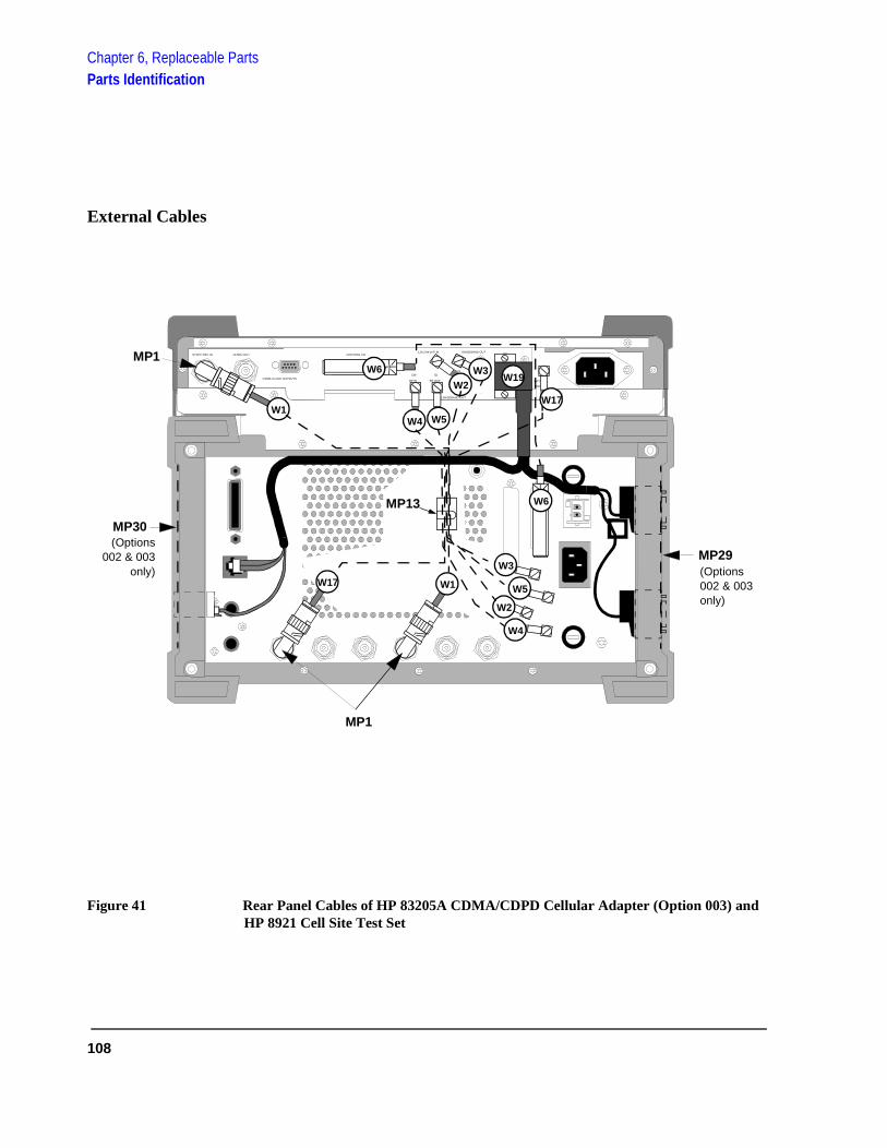
Chapter 6, Replaceable PartsParts Identification
External Cables
Figure 41 Rear Panel Cables of HP 83205A CDMA/CDPD Cellular Adapter (Option 003) and HP 8921 Cell Site Test Set
114.3 MHz IF IN I BASEBAND OUT
AUXCW
RF IN
IQ
RF OUT OPTIONAL
SE
RIA
L P
OR
T
CONTROL I/OSYNTH REF IN 10 MHz OUT
CDMA CLOCK OUTPUTSDSP IN
MOD OUT
10 MHz
REF OUT
Q BASEBAND OUT
W5
W2
W1
W3
MP13 W6
W5W4
W2W3
W1W17
W6
W17
W19
MP1
MP1
MP29
MP30(Options
002 & 003only) (Options
002 & 003 only)
W4
108

Chapter 6, Replaceable PartsParts Identification
Front Panel Components
Figure 42 Front Panel Components
Frame
Top View
Front View
PWR REFUNLOCK
83205AC D M A C E L L U L A R A D A P T E R
RF IN/OUTTO
TEST SET
RF IN/OUTMAX.PWR 60WCONTINUOUS
DIAGNOSTICMONITOR OUT
1.2288 MHz OUTCHIP CLOCK
19.6608 MHz OUT16 X CHIP CLOCK
CDMATIMEBASE IN
EVEN SECOND/SYNC IN
DATAIN
TRIGGER/QUALIFIER IN
A4 Assembly
A1W1
Deck
A2 Assembly
J702J701
J703J1
J707J705
J706
A1 Assembly
MP4
MP3MP5 MP5
MP4
MP2
MP4
MP4
MP4MP4
MP2
MP4
MP4
MP4
MP4
MP4
MP4
MP3
MP15
A1MP3
A1W5
A1MP1
A1MP2
A1MP4
A1W2
A1W4
A1W3
A1W7
A1W6
Dress Plate
RFI Braid
MP4
W9(4J701-5J709)
MP24
109

Chapter 6, Replaceable PartsParts Identification
Cover and Rear Panel Components
Figure 43 Cover and Rear Panel Components
Deck
114.3 MHz IF IN I BASEBAND OUT
AUXCW
RF IN
IQ
RF OUT OPTIONAL
SE
RIA
L P
OR
T
CONTROL I/OSYNTH REF IN 10 MHz OUT
CDMA CLOCK OUTPUTS
DSP IN
MOD OUT
10 MHzREF OUT
Q BASEBAND OUT
MP28
Top View
MP 18 (cover side view)
MP7MP7MP8
MP14
MP4 MP4
MP7MP7
MP16(Rear Panel)
(Mounting Plate)
(Option 001)MP17
110

Chapter 6, Replaceable PartsParts Identification
Rear Panel Components
Figure 44 Rear Panel Components
MP14
Deck
J5 J2
MP20
MP19 BNC Connector
MP16
MP17
MP14
W7 W23
W15
MP4
(Opt 001 only)
114.3 MHz IF IN I BASEBAND OUT
AUXCW
RF INIQ
RF OUT
OPTIONAL
SE
RIA
L P
OR
T
CONTROL I/OSYNTH REF IN 10 MHz OUT
CDMA CLOCK OUTPUTSDSP IN
MOD OUT
10 MHzREF OUT
Q BASEBAND OUT
W26(OJ3)
W25(OJ2)
W24(OJ1)W7W23
W27(OJ4)
W28(OJ5)
W8(OJ6)
(Lock Washer)
(9/16” Nut)
(Back Panel)
Drawing B
MP23
MP22MP4
(Rear Panel)
0J3
0J7MP27
MP26
MP14
Cable Clips
SMC Connector
0 J 3
(Lock Washer)
(1/4” Nut)
(Back Panel)
Drawing A
(OJ8 -11J6)(See Drawing A)
(See InsetDrawing A)
(See Drawing B)(Opt 002/003)
111
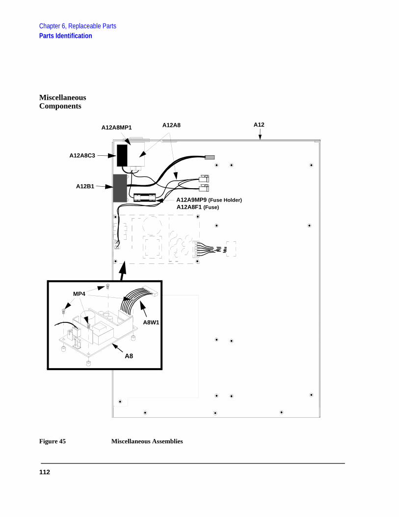
Chapter 6, Replaceable PartsParts Identification
Miscellaneous Components
Figure 45 Miscellaneous Assemblies
A8
A12A8C3
A12A8MP1 A12A8
A12B1
A12
A12A8F1 (Fuse)A12A9MP9 (Fuse Holder)
A8W1
MP4
112

Chapter 6, Replaceable PartsParts Identification
A4 Gen./Ref. Assembly and Components
NOTE: Perform the PER_CALD and EBNO_CAL calibration procedures after replacing the A4assembly, see "Periodic Calibration (for Options 001 & 003 only)" on page 127.
Figure 46 A4 Generator/Reference Assembly
J11
SMB Connector
P/O A12B1
J400J500
J708J401
J7
J9
J10
A4 Assembly
J20J5
J2
J3
J709
J11
(4J11-10J2)W22
W23
W7(A4J5-[RP]10 MHz OUT)
(A4J2-[RP] SYNTH REF IN)
A1W7A1W6
A1W4 A1W5
A1W3 W9
A1W1
W16
(A8W1)(A12B1)
W34
J20 J9
(J10)J709 J4
W33 W32
W31
W30
W29(4J400-5J401)
(4J500-5J501) (4J708-5J4)
(4J401-7J5)
(4J3-6J2)
(4J7-2J4)
J702J701
J703J1
J707J705
J706
J11 (W22)(4J11-10J2)
A1W7 (4J706- [FP]19.6608 MHz OUT)
A1W6 (4J705- [FP] 1.2288 MHz OUT CHIP CLOCK)
A1W4 (4J1- [FP] CDMA TIMEBASE IN)A1W5 (4J707- [FP] DIAGNOSTIC MONITOR OUT)
A1W3 (4J703-[FP] EVEN SECOND/SYNC IN)W9 (4J701-5J709)
A1W1 (4J702-[FP] TRIGGER/QUALIFIER IN)W16
MP4
MP4
MP4MP4
MP4
MP4
MP4
W28
Assembly A7, Connector J5
to Assembly A4, Connector J3
(7J5-4J3)Wirereferencedesignator
Cable Legend
[RP] = Rear Panel[FP] = Front Panel
113

Chapter 6, Replaceable PartsParts Identification
A9 Reference/IQ Assembly
NOTE: Perform the PER_CALD and EBNO_CAL calibration procedures after replacing the A4assembly, see "Periodic Calibration (for Options 001 & 003 only)" on page 127.
Figure 47 A9 Reference/IQ Assembly
A9 Assembly
MP10
W37W24
W30
A6 SubassemblyA7 Subassembly
A9 Assembly
W27W35
W28
W31
Ribbon Cable (W16)
(6J2-4J3)
W20(6J6-11J3) (6J3-[RP]OJ1) (6J4-2J6)
(7J5-4J401)
(7J4-[RP]OJ5)
W36(7J3-5J400)
W21(7J6-11J4)
(7J2-5J500)(7J1-[RP]OJ4)
MP10
MP10
MP10
MP10
MP10
W28
Assembly A7, Connector J5
to Assembly A4, Connector J3
(7J5-4J3)Wirereferencedesignator
Cable Legend
[RP] = Rear Panel[FP] = Front Panel
114

Chapter 6, Replaceable PartsParts Identification
A10 Directional Coupler & Serial Switch Assembly
Figure 48 A10 CDPD Directional Coupler and Serial Switch Assembly
A10
Rear Panel
A10 Assembly
W10
W11
W22
W12
P/O A8W1
W14
J1J2
J4J3
A10 Assembly
W10
W14
W11
Coupler Side
W12(10J1-11P2)
P/O A8W1
(10J2-4J24)W22
Switch Side
OUTPUT
INPUT
−30dB
(A10 “−30dB”-11J5)
(A10 “INPUT”-front panelRF IN/OUT)
(A10 “OUTPUT”-front panel RF IN/OUT TO TEST SET)
115

Chapter 6, Replaceable PartsParts Identification
A11 CDPD Assembly
Figure 49 A11 CDPD Assembly (on Options 002 & 003 only)
W12 (11P2-10J1)
W13 (11P3-2J9)
W22 (11J2-10J2)
A11 Assembly
MP11
MP11
MP11
MP11
W21 (11J4-7J6)
W20 (11J3-6J14)
W15 (11J6-[RP]MODE OUT)
W14 (11J5-DIR. COUPL.)
116

Chapter 6, Replaceable PartsParts Identification
Semi-Rigid Cables & Components
Figure 50 Semi-Rigid Cables and Components
A10 Assembly
W10 (Semi-rigid cable)
W11 (Semi-rigid cable)
MP12
W14
MP12
MP13
MP13
MP12
117

Chapter 6, Replaceable PartsParts Identification
A2 RX DSP Assembly
Figure 51 A2 RX DSP Assembly
A5 Data Buffer Assembly
Figure 52 A5 Data Buffer Assembly
A2 Assembly
W29 (2J4-4J7)
W37 (2J6-6J4)
A5A2
MP11
MP11W13 (2J9-11P3)
(2J3-OJ2)W25
A5 AssemblyA5
W8
W35W33
W34 W36
W26W9 (4J701-5J709)
W32 (5J4-4J708)
(5J502-OJ6)
(5J500-7J2)(5J501-4J500)
(5J401-4J400)(5J400-7J3)
(5J402-OJ3)
(J709)
(J22)
A1W2 (to front panel DATA IN)
118

Chapter 6, Replaceable PartsParts Identification
A3 Motherboard Assembly
Figure 53 A3 Motherboard Assembly
MP12
MP12
A3K1
A3
MP12
MP12
119

Chapter 6, Replaceable PartsParts List
Parts List
REFERENCE DESCRIPTION PART DESIGNATOR NUMBER
ACC1 MANUAL ALR 83205-90009
ACC2 USER’S GUIDE 83205-90008
ACC3 SW USER GUIDE 83204-90014
ACC4 DSP/CDPD UPGRADE KIT 83205-61801
ACC5 CDPD SFTWARE KIT 83204-61807
ACC6 KIT-RACK MOUNT 08921-61037
ACC7 ACCESSORY KIT 83204-61008
ACC7AT1 ATTN COAX 6dB 1W 0955-0698
ACC7MP1 ADPT TEE FMF BNC 1250-0781
ACC7MP2 TERMINATION 0960-0053
ACC7MP3 ADPT M BNC F SMA 1250-1700
ACC7MP4 ADAPTER 1250-1250
ACC7W1 CA MCND RJ11-DB9 08921-61038
ACC7W2 CA CX ASSY 50Z 8120-2582
ACC7W4 CBL FLEX COAX 08921-61052
A1 (#001) AY FRNT PNL #001 83205-61005
A1 (#002) AY FRNT PNL #002 83205-61003
A1 (#003) AY FRNT PNL #003 83205-61001
A1MP1 (#001) FRAME FRONT 83201-21007
A1MP1 (#002/#003) FRAME FRONT MACH 83203-21003
A1MP2 (#001) PANEL DRESS 83205-00002
A1MP2 (#002) PANEL DRESS #002 83205-00001
A1MP2 (#003) PANEL DRESS 83203-00025
120
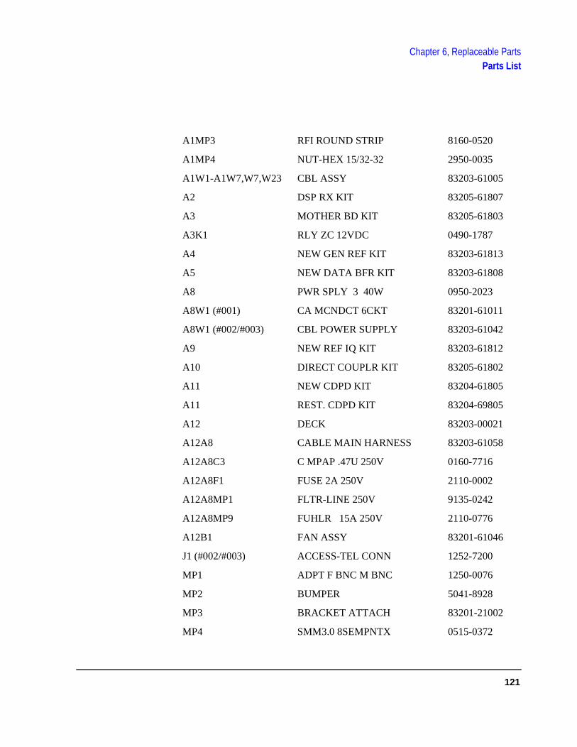
Chapter 6, Replaceable PartsParts List
A1MP3 RFI ROUND STRIP 8160-0520
A1MP4 NUT-HEX 15/32-32 2950-0035
A1W1-A1W7,W7,W23 CBL ASSY 83203-61005
A2 DSP RX KIT 83205-61807
A3 MOTHER BD KIT 83205-61803
A3K1 RLY ZC 12VDC 0490-1787
A4 NEW GEN REF KIT 83203-61813
A5 NEW DATA BFR KIT 83203-61808
A8 PWR SPLY 3 40W 0950-2023
A8W1 (#001) CA MCNDCT 6CKT 83201-61011
A8W1 (#002/#003) CBL POWER SUPPLY 83203-61042
A9 NEW REF IQ KIT 83203-61812
A10 DIRECT COUPLR KIT 83205-61802
A11 NEW CDPD KIT 83204-61805
A11 REST. CDPD KIT 83204-69805
A12 DECK 83203-00021
A12A8 CABLE MAIN HARNESS 83203-61058
A12A8C3 C MPAP .47U 250V 0160-7716
A12A8F1 FUSE 2A 250V 2110-0002
A12A8MP1 FLTR-LINE 250V 9135-0242
A12A8MP9 FUHLR 15A 250V 2110-0776
A12B1 FAN ASSY 83201-61046
J1 (#002/#003) ACCESS-TEL CONN 1252-7200
MP1 ADPT F BNC M BNC 1250-0076
MP2 BUMPER 5041-8928
MP3 BRACKET ATTACH 83201-21002
MP4 SMM3.0 8SEMPNTX 0515-0372
121
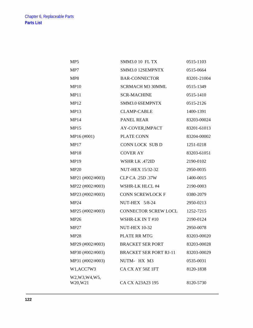
Chapter 6, Replaceable PartsParts List
MP5 SMM3.0 10 FL TX 0515-1103
MP7 SMM3.0 12SEMPNTX 0515-0664
MP8 BAR-CONNECTOR 83201-21004
MP10 SCRMACH M3 30MML 0515-1349
MP11 SCR-MACHINE 0515-1410
MP12 SMM3.0 6SEMPNTX 0515-2126
MP13 CLAMP-CABLE 1400-1391
MP14 PANEL REAR 83203-00024
MP15 AY-COVER,IMPACT 83201-61013
MP16 (#001) PLATE CONN 83204-00002
MP17 CONN LOCK SUB D 1251-0218
MP18 COVER AY 83203-61051
MP19 WSHR LK .472ID 2190-0102
MP20 NUT-HEX 15/32-32 2950-0035
MP21 (#002/#003) CLP CA .25D .37W 1400-0015
MP22 (#002/#003) WSHR-LK HLCL #4 2190-0003
MP23 (#002/#003) CONN SCREWLOCK F 0380-2079
MP24 NUT-HEX 5/8-24 2950-0213
MP25 (#002/#003) CONNECTOR SCREW LOCL 1252-7215
MP26 WSHR-LK IN T #10 2190-0124
MP27 NUT-HEX 10-32 2950-0078
MP28 PLATE RR MTG 83203-00020
MP29 (#002/#003) BRACKET SER PORT 83203-00028
MP30 (#002/#003) BRACKET SER PORT RJ-11 83203-00029
MP31 (#002/#003) NUTM- HX M3 0535-0031
W1,ACC7W3 CA CX AY 50Z 1FT 8120-1838
W2,W3,W4,W5,W20,W21 CA CX A23A23 195 8120-5730
122

Chapter 6, Replaceable PartsParts List
W6 CA MCNDCT 37CKT 83201-61001
W8,W24,W25,W26 FLEX CABLE 83203-61013
W9 CABLE AY 3 PIN 83203-61020
W10 (#002/#003) CA SR-2.18 N-SMA 83203-61045
W11 (#002/#003) CA SR-2.18 N-SMA 83203-61046
W12 (#002/#003) CA ASSY 3COND 83203-61048
W13 (#002/#003) CBL RCV/CDPD 83203-61049
W14 (#002/#003) CA COAX SMA-SMC 83203-61047
W15,W27,W28 (#002/#003) CX F SMC-SMCBH 8 8120-5857
W16 RBN 15CNDCT 28AWG 83201-61004
W17 (#002/#003) CABLE 8120-6285
W18 (#002/#003) CX FLEX N-N 8120-8317
W19 (#002/#003) CBL SERIAL PORTS 83203-61044
W22, (#002/#003) CA ASSY 4-COND 83203-61043
W29,W30 COAX CABLE ASSY 8120-5017
W31 COAXIAL CBL ASSY 8120-5022
W32 CX F SMB-F SMB 83203-61017
W33,W34 CX F SMB-F SMB 83203-61018
W35,W36 FLEX CABLE 83203-61019
W37 CA CX A06A06 260 8120-5020
123

Chapter 6, Replaceable PartsParts List
124
7
Periodic Calibration and Performance Tests
This chapter contains the calibration procedures and the CDMA and CDPD performance test procedures for the HP 83205A Cellular Adapter.
125

Chapter 7, Periodic Calibration and Performance TestsIntroduction
Introduction
NOTE: For Cellular Adapter Options 001 and 003, perform the "Periodic Calibration (for Options001 & 003 only)" on page 127 before performing any of the performance tests.
The performance tests in this chapter verify that the Cellular Adapter performs to its specifications. Use table 14 to determine the calibration and performance tests to run for each of the following Cellular Adapters:
• HP 83205A CDMA Cellular Adapter Option 001• HP 83205A CDPD Cellular Adapter Option 002• HP 83205A CDMA/CDPD Cellular Adapter Option 003
The "CDMA Performance Record" on page 137 and "CDPD Performance Record" on page 138 are provided for logging the results of these test routines.
Table 14 Calibration and Performance Tests
Performance Test Name HP 83205A Cellular Adapter
Option 001 Option 002 Option 003
"Periodic Calibration (for Options 001 & 003 only)" on page 127
X X
"CDMA Performance Test (for Options 001 & 003 only)" on page 129
X X
"CDPD Performance Test (for Options 002 & 003 only)" on page 131
X X
126

Chapter 7, Periodic Calibration and Performance TestsPeriodic Calibration (for Options 001 & 003 only)
12 d
t Set’s
Periodic Calibration (for Options 001 & 003 only)
The following calibration procedures only apply to the Cellular Adapters containing CDMA (Options 001 & 003). A CDMA Cellular Adapter is calibrated by running the PER_CALD and EBNO_CAL calibration programs. These programs are stored in the Test Set’s ROM and should be run at least everymonths, or whenever the Test Set and Cellular Adapter are disconnected anreassembled.
NOTE: Before calibrating the Test Set and CDMA Cellular Adapter as a Test System, ensure the Test Set has been calibrated independently of the Cellular Adapter. Refer to the TesALR manual for calibrating the Test Set.
PER_CALD Calibration Procedure
1. Press TESTS to access the TESTS screen.
2. Select the Procedure Location: field.
3. Select ROM under the Choices: menu.
4. Select the Procedure Filename: field.
5. Select PER_CALD under the Choices: menu.
6. Select Run Test (k1 USER key).
7. Follow the instructions on the screen.
The end of the PER_CALD routine will instruct you to exit this program and cycle the power Off and On.
127

Chapter 7, Periodic Calibration and Performance TestsPeriodic Calibration (for Options 001 & 003 only)
T
EBNO_CAL Calibration ProcedureThis calibration procedure will take several minutes, and during calibration, you will be required to disconnect and reconnect the Cellular Adapter’s IQ RF OUport to the Test Set.
NOTE: The preceding PER_CALD Calibration Procedure must be completed prior to performingthe following procedure.
1. Connect the Cellular Adapter’s IQ RF OUT to the Test Set’s ANT IN connector.
2. Press the TESTS to access the TESTS screen.
3. Select the Procedure Location: field.
4. Select ROM under the Choices: menu.
5. Select the Procedure Filename: field.
6. Select EBNO_CAL under the Choices: menu.
7. Select Run Test (k1 USER key).
8. Follow the instructions on the screen.
9. If the EBNO_CAL calibration corrections are less than 1.27dB, respond YES to use these corrections as the new calibration factors.
The end of the EBNO_CAL routine will instruct you to exit this calibration program and cycle the power Off and On.
128

Chapter 7, Periodic Calibration and Performance TestsCDMA Performance Test (for Options 001 & 003 only)
CDMA Performance Test (for Options 001 & 003 only)
CDMA performance verification is done by setting the Test System into a loop back state and using the CDMA analyzer to measure the CDMA generator. This allows you to quickly and accurately verify that both the generator and analyzer are working. No external test equipment is needed.
Prerequisites Perform the "Periodic Calibration (for Options 001 & 003 only)" on page 127 before performing the following performance procedure.
Equipment Setup Make sure the back panel connections between the Test Set and the Cellular Adapter are properly connected. For reference, see figure 16, "Rear Panel Cable Connections for HP 83205A CDMA/CDPD Cellular Adapter," on page 65.
CDMA Performance Procedure
Step 1. Connect the Test Set’s DUPLEX OUT to the ANT IN port.
Step 2. Press the PRESET key or cycle power to the Test System.
Verify the REF UNLOCK LED is not lit, otherwise, troubleshoot the Test System, see "Test System Troubleshooting" on page 38.
Step 3. Set up the CDMA GENERATOR screen
• Select More: and then CDMA GEN from the Choices: menu. The CDMA GENER-ATOR screen appears.
• Set the RF Gen Freq field to 850 MHz.
• Set the Amplitude field to −10 dBm.
• Set the CW RF Path field to IQ.
• Set the Output Port field to Dupl.
• Set the Gen Dir field to Fwd.
129

Chapter 7, Periodic Calibration and Performance TestsCDMA Performance Test (for Options 001 & 003 only)
Step 4. Set up the CDMA ANALYZER screen
a. Select More:, and then CDMA ANL from the Choices: menu. The CDMA ANALYZER screen appears.
b. Select the Measurement field and change it to Rho , see figure 54.
c. Set the Tune Freq field to 850 MHz.
d. Set the Input Atten field to 20 dB.
e. Set the Input Port field to Ant.
Figure 54 CDMA Analyzer Screen
Step 5. Read and record the Rho measurement, see figure 54.
a. This reading should be >0.96 and no error messages should appear.
b. Record the rho measurement in the "CDMA Performance Record" on page 137.
Tune Freq To Screen
CDMA ANALYZER
Frequency Error
Anl Special
Synth Ref
PN Offset
Meas Intvl
Gain
Analyzer
Qual Event
0
850.000000MHz
RF GENRF ANLAF ANLSCOPESPEC ANLENCODEDECODERADIO INT
Rho
Even Sec In
Anl Dir
Set to 20 dB
Off
Hz
More
80 ms
Set to 850 MHz IQ
0.9903
Input Atten20 dB
Input PortRF In/Ant
CDMA TB
Internal
0.00
Enable/Not
0.50
Auto/Hold
Fwd/Rev
Arm MeasSingle/ContDisarm
12 dB
ms
Trig EventImmed
Time Offset us Carrier Feedthru
-47.5dB
-50 50- - - -
Set Measurement field to Rho
Set to ANT
2.39
Read Rho measurement
130

Chapter 7, Periodic Calibration and Performance TestsCDPD Performance Test (for Options 002 & 003 only)
CDPD Performance Test (for Options 002 & 003 only)
The spectral purity, modulation accuracy, and on/off level of the CDPD Generator are measured directly with the CDPD analyzer.
Prerequisites Perform the "Periodic Calibration (for Options 001 & 003 only)" on page 127 before performing the following performance procedure.
Equipment Set Up No external test equipment is required.
Procedure Step 1. Load the CDPD MDBS Cell Site Test Software.
a. Press the PRESET key.
b. Insert the CDPD MDBS Cell Site Test Software card, HP 83204-61807.
c. Press the TESTS key.
d. Select Card for procedure location and CDPD for procedure filename.
e. Run the test, press k1 (Run Test). Wait (30 seconds to 2 minutes) for the (CDPD) Main Menu to appear, see figure 55.
Figure 55 Main Menu (CDPD)
1
Continue2
Help4
RF GENTo Screen
RF ANLAF ANL
TESTS (Main Menu)
LOAD TEST PROCEDURE:Select Procedure Locat ion:
Select Procedure F i lename:
Description:
Library: Program:
CUSTOMIZE TEST PROCEDURE: SET UP TEST SET:
Channel In format ionTest ParametersOrder of TestsPass/Fai l L imi tsSave/Delete Procedure
External DevicesPrinter Setup
IBASIC Cnt r l
FreqParmSeqnSpecProc
CnfgPrint
Exec Execut ion Cond
IBASIC
RF parametric tests for CDPD MDBS equipment.
Choices:
CDPDCALSLDEMOSEQN
Card
Run Test
CDPD
Select Card as the location of the diagnostic program.
Select the CDPD diagnostic program.
Main Menu (CDPD)
CDPD Card
Revision : A.00.11
CDPD MDBS CELL SITE TEST
TX Tests
RX Tests2
4
3
End5
1
MAIN MENU==== ====(1) Transmitter Tests(2) Receiver Tests(3) System Tests(4) Calibrations (5) End this Program
System
Use knob or softkeys to select from the menu.
Cals
TESTS (IBASIC Controller)
131

Chapter 7, Periodic Calibration and Performance TestsCDPD Performance Test (for Options 002 & 003 only)
e.
Step 2. Calibrate and record the GMSK Deviation.
a. From the MAIN MENU, select (4) Calibrations. The CALIBRATIONS menu appears, see figure 56.
Figure 56 CALIBRATIONS Menu
b. From CALIBRATIONS menu, select (3) GMSK Deviation Calibration, an equipment cable-hookup screen appears.
c. Connect Test Set and Cellular Adapter as shown on the screen, that is, connect the Test Set’s RF IN/OUT to Cellular Adapter’s RF IN/OUT TO TEST SET.
d. Press the k2 (Continue). Wait for the GMSK Deviation Calibration mea-sured value to appear, figure 57. WRITE DOWN the measured value for later us
Figure 57 GMSK Deviation
e. Press k5 (Menu) to return to the CALIBRATIONS menu.
f. From the CALIBRATIONS menu, press k5 (Prev Menu) to return to the MAIN MENU screen.
Power2
4
To Screen
3
Prev Menu5
CALIBRATIONS ============(1) Cable Loss(2) Power Measurement Calibration(3) GMSK Deviation Calibration(4) Center Frequency Calibration(5) Previous Menu
GMSK Dev
Cntr Freq
2
4
3
Menu5
1
RF parametric tests for CDPD MDBS equipment====================================================Test conditions Measured value P/F
====================================================
GMSK Deviation Calibration 8.52 kHz/V
TESTS (IBASIC Controller)
132

Chapter 7, Periodic Calibration and Performance TestsCDPD Performance Test (for Options 002 & 003 only)
e
Step 3. Perform Transmitter Tests.
a. From the MAIN MENU, select (1) Transmitter Tests. The TRAMSMITTER TESTS menu appears, see figure 58.
Figure 58 Transmitter Tests Menu
b. Select (1) RF Parameters, or press the k1 key.
c. Connect the Test Set and Cellular Adapter as shown on the screen. Do not connect the Cellular Adapter to the base station. (Test Set’s RF IN/OUT is still connected to Cellular Adapter’s RF IN/OUT TO TEST SET.)
d. Press k2 (Continue). The TESTS (IBASIC Controller) screen reports No signal found.
e. Press SHIFT and CANCEL keys.
f. Connect the Test Set’s DUPLEX OUT connector to its ANT IN connector.
g. Move the cursor to the message block and enter OUTPUT 10;"XMIT_MDBS 2", see figure 59. Use the Test Set’s cursor control knob to select each character from thchoices menu and then select DONE.
h. Change the output statement to OUTPUT 10;"WR_AMPL_OFF". After entering, select DONE.
Figure 59
RF Parms
Pwr Cal2
4
3
Prev Menu5
1
TRANSMITTER TESTS=========== =====(1) RF Parameters (power, frequency, etc.)(2) Power Measurement Calibration(3) Previous Menu
Use knob or softkeys to select from the menu.TESTS (IBASIC Controller)
2
3
1OUTPUT 10;"XMIT_MDBS 2"
TESTS (IBASIC Controller)
133

Chapter 7, Periodic Calibration and Performance TestsCDPD Performance Test (for Options 002 & 003 only)
Step 4. Setup the RF GENERATOR screen.
a. Select RF GEN from the To Screen menu. The RF GENERATOR screen appears, see figure 60.
b. Set RF Gen Freq to 870 MHz.
c. Set Amplitude to −20 dBm.
d. Turn ON the Mod In To, press the ON/OFF key. Verify that the value in this field is the same as the GMSK Deviation Calibration value recorded in step 2d.
e. Change FM Coupling AC/DC to AC/DC and perform DC FM Zero by pressing the Cursor Control knob.
Figure 60 Setting up the RF GENERATOR Screen for the CDPD Performance Test
RF Gen Freq To Screen
RF GENERATOR
FM Deviation
Amplitude
AFGen1 Freq
AFGen1 To
AFGen2 Freq
AFGen2 To
Mic Pre-Emp
Mod In To-20.00
870.000000
dBm
RF GENRF ANLAF ANLSCOPESPEC ANLENCODEDECODERADIO INT
TX Freq Frequency
TX Power
FM
FM Coupling Audio OutAtten Hold
Output Port
MHz
RF Out/Dupl
OFF
Enter −20 dBm.
Enter 870 MHz.
On/Off
Off
Off SINAD Off
Off
MoreAC/DCDC FM Zero
FM (/Vpk)8.52
kHz
Change AC/DC to AC/DC Turn ON (press the ON/OFF key)and verify the value.and perform DC FM Zero.
134

Chapter 7, Periodic Calibration and Performance TestsCDPD Performance Test (for Options 002 & 003 only)
Step 5. Setup the RF ANALYZER screen.
a. Select RF ANL from the To Screen menu. The RF ANALYZER screen appears, see figure 61.
b. Set Tune Mode to Manual.
c. Set Tune Freq to 870 MHz.
d. Set Input Port to Ant.
Figure 61 RF ANALYZER Screen
Step 6. Access the CDPD SCREEN.
a. Select More from the To Screen menu.
b. Select CDPD TEST. The CDPD SCREEN appears, see figure 62.
c. Set Digital Anl to Cont.
d. Verify Status is 3.000000.
Figure 62 CDPD SCREEN
Tune Mode To Screen
Tune Freq
Input port
Input Atten
IF Filter
Squelch
Ext TX Key
TX Pwr Zero870.000000
Auto/Manual
MHz
RF GENRF ANLAF ANLSCOPESPEC ANLENCODEDECODERADIO INT
TX Power
Sensitivity RF Cnt Gate
Set to 870 MHz.
Set to Ant. Off SINAD Off
More
Zero
Set to Manual.RF In/Ant
Digital Anl
To Screen
CDPD SCREEN
Measurement
Gain
Arms Meas
Special
RF GENRF ANLAF ANLSCOPESPEC ANLENCODE
Single/ContDisprm
Ampl Cntl
Dig An1:Armed
Dig Gen:Idle
StatusFreq Err Mod IndxMod IndxIncid FMMx Freq Chan PwrAdj PwrAlt PwrAl2 PwrMax ADCGain Set
Hz
SDHz
DevdB
dBcdBcdBcdBa
db
3.000000-189.400000
0.5000000.000223
57.3569874556.40526-18.128560-34.478719-70.270158-73.895623
-6.20052112.000000
Set to Cont.
Adj Pwr dBcAlt Pwr dBcAl2 Pwr dBc
Chan Pwr dB
RECORD:
Mod IndxStatus
135

Chapter 7, Periodic Calibration and Performance TestsCDPD Performance Test (for Options 002 & 003 only)
Step 7. Record CDPD SCREEN information.
a. Record the Adjacent Channel Power, Adj Pwr dBc (see figure 62 on page 135), in the "CDPD Performance Record" on page 138.
b. Record the First Alternate Channel power, Alt Pwr dBc, in the "CDPD Performance Record" on page 138.
c. Record the Second Alternate Channel power, Al2 Pwr dBc, in the "CDPD Performance Record" on page 138.
d. Record the Modulation Index, Mod Indx, in the "CDPD Performance Record" on page 138.
Step 8. Calculate On/Off Power Level
a. Record the present value for channel power, Chan Pwr dB, as ON POWER in the equation below and in the "CDPD Performance Record" on page 138.
b. Change Ampl Cntrl to CDPD, see figure 63.
Figure 63 CDPD SCREEN
c. Record the Chan Pwr dB of the CDPD SCREEN as OFF POWER in the equation below and in the "CDPD Performance Record" on page 138.
d. Calculate in the equation below the ON/OFF DIFFERENTIAL level and record it in the "CDPD Performance Record" on page 138.
ON POWER − OFF POWER = ON/OFF DIFFERENTIAL
___________− ___________ = _________
Digital Anl
To Screen
CDPD SCREEN
Measurement
Gain
Arms Meas
Special
RF GENRF ANLAF ANLSCOPESPEC ANLENCODEDECODERADIO INT
Single/ContDisprm
Ampl Cntl
Valid Check
Dig An1:Armed
Dig Gen:Idle
StatusFreq Err Mod IndxMod IndxIncid FMMx Freq Chan PwrAdj PwrAlt PwrAl2 PwrMax ADCGain Set
Hz
SDHz
DevdB
dBcdBcdBcdBa
db
3.000000-192.400000
0.5000000.000223
104.3569875130.40526-38.488560-34.478719-58.270158-58.895623
-8.20052130.000000
Set to CDPD.
Chan Pwr dB
Norm/CDPD
136

Chapter 7, Periodic Calibration and Performance TestsCDMA Performance Record
CDMA Performance Record
Date _____________ Time_______________ Humidity ___________
Tested by: __________________________________________________
Cellular Adapter Serial Number: _________________________________
Test Set Serial Number ________________________________________
Test Set Last Calibration Date __________________
Rho Measurement
HP 83205A CDMA Cellular Adapter (Opt 001)
HP 83205A CDMA/CDPD Cellular Adapter (Opt 003)
Rho
Lower Limit Actual
0.96
137

Chapter 7, Periodic Calibration and Performance TestsCDPD Performance Record
CDPD Performance Record
Date _____________ Time_______________ Humidity ___________
Tested by: __________________________________________________
Cellular Adapter Serial Number: _________________________________
Test Set Serial Number ________________________________________
Test Set Last Calibration Date __________________
CDPD Generator Spectral Purity Measurement
CDPD Modulation Accuracy Measurement
CDPD Generator On/Off Level Measurement
1. ON POWER − OFF POWER = ON/OFF DIFFERENTIAL
HP 83205A CDPD Cellular Adapter (Opt 002)
HP 83205A CDMA/CDPD Cellular Adapter (Opt 003)
Channel Power Upper Limit (dBc) Measured Spectral PurityActual (dBc)
Adjacent Channel Power (Adj Pwr dBc) −26
First Alternate Channel (Alt Pwr dBc) −45
Second Alternate Channel (Al2 Pwr dBc) −60
Upper Limit Lower Limit Modulation Index (Mod Indx)
0.525 0.475
Measured Values Calculated Value (dB)
ON POWER OFF POWER ON/OFF DIFFERENTIAL1 Actual
Lower Limit
15
138

8
Specifications
This chapter contains the specifications for the HP 83205A CDMA and CDPD Cellular Adapters. Chapter 7, "Periodic Calibration and Performance Tests," on page 125 has the performance tests for verifying measurement performance.
139
Chapter 8, SpecificationsHP 83205A CDMA Specifications
r’s and tire
HP 83205A CDMA Specifications
The following specifications describe the HP 83205A CDMA Cellular Adaptewarranted performance when operating with an HP 8921A Cell Site Test Setapply after a 30 minute warm-up. All specifications are valid over the unit’s enoperating/environmental range unless otherwise noted.
Supplemental characteristics are intended to provide additional information useful in applying the instrument by giving typical, but non-warranted performance parameters. These are shown in italics or labeled as “typical”, “usable to”, or “nominal”.
NOTE: The following specifications describe the CDMA Test Systems: HP 8921A Option 600(HP 8921A Test Set & HP 83205A CDMA Cellular Adapter) and HP 8921A Option 603(HP 8921A Test Set & HP 83205A CDMA/CDPD Cellular Adapter).
CDMA Signal Generator
Frequency & Amplitude
Frequency Range: 824 to 894 MHz, usable from 800 MHz to 1000 MHz and from 4 MHz to 200 MHz with degraded ρ and carrier feedthrough performance.
Frequency Resolution: 1 Hz
Output Level Range:at Test Set’s RF IN/OUT: −19 dBm to −137 dBmat Test Set’s DUPLEX OUT: +4 dBm to −127 dBm
Output Level Accuracy:at Test Set’s RF IN/OUT: ±2.0 dB, typically ±1.0 dBat Test Set’s DUPLEX OUT: ±1.7 dB, typically ±1.0 dB
Modulation
Reverse Link Source Modulation: OQPSK per TIA IS-95
Reverse Link Source Modulation Data: Internal data buffer, Idle (all zeroes)NOTE: May also be modulated with external encoded data. External data must be properly coded and ready for short sequence spreading at 1.2288 Mbit per second.
Forward Link Source Modulation: QPSK per TIA IS-95
140

Chapter 8, SpecificationsHP 83205A CDMA Specifications
Forward Link Source Modulation Data: Internal (Pilot channel) NOTE: May also be modulated with external encoded data. External data must be properly coded and ready for short sequence spreading at 1.2288 Mbit per second.
Residual Rho (ρ): 0.96, typically >0.98 at 25°C ±15°C
Carrier Feedthrough: −30dBc, typically <−35 dBc at 25°C ±15°C
Adjacent Channel Noise: −45dBc, typically <−50 dBc; measured in a 30 kHz BW filter relative to the total carrier power at fc ±900 kHz at 25°C ±15°C;from RF IN/OUT connector <−29 dBm from DUPLEX OUT connector <-3 dBm
PN Offset: Adjustable from 0 to 511 units (1 unit equals 64 chips)
PN Offset Resolution: 0.0156 units (1 chip)
Data Buffer
Size/Length: 5400 frames
Modes: Single, Continuous Looping, and Idle
Coding: IS-95 CDMA full rate reverse link channel coding, interleaving, and spreading
Long Code Mask: 42 zeros
Input Data Rate: 9600 bps; 14,400 bps
Data Source: For each rate set, 300 frames factory loaded, 1800 frames additional user definable data can be entered via HP-IB
141
Chapter 8, SpecificationsHP 83205A CDMA Specifications
r of
AWGN Source(Added White Gaussian Noise)
Bandwidth: 2 MHz nominally, Gaussian to >3 sigma
Modes: Noise only, data only, and user selectable Eb/No settings
Eb/No Resolution: 0.1 dB
Eb/No Range: −5 to 25 dB
Eb/No Accuracy: ±0.5 dB, for Eb/No of 5 to 20 dBtypically ±1 dB for Eb/No of −5 to +5 dB and +20 dB to +25 dB
CDMA Analyzer Wave Quality Measurement Rho (ρ)IS-95 forward or reverse link formats (QPSK or OQPSK)
Input and Level Range:at Test Set’s RF IN/OUT: −10 dBm to +48 dBmat Test Set’s ANT IN: −46 dBm to +17 dBm
Input Frequency Range: 4 MHz to 1000 MHz
Rho (ρ) Measurement Interval Range: 0.25 to 1.25 ms
Rho (ρ) Measurement Range: 0.50 to 1.00
Rho (ρ) Measurement Accuracy: <±0.005
Input Frequency Error Range: ±900 Hz
Frequency Error Measurement Accuracy: ±30 Hz using a measurement interval ≥ 0.5 ms. NOTE: Accuracy can be improved by averaging a numbemeasrements. Error is reduced by square root of the number of averages.
Other Reported Parameters: Pilot Time Offset, Carrier Feedthrough, Error Vector Magnitude, Amplitude Error and Phase Error
Pilot Time Offset Measurement Accuracy: Typically <±500 ns from even-second signal to start of PN sequence
142

Chapter 8, SpecificationsHP 83205A CDMA Specifications
cy)
e or
Average Power Measurement
Input Frequency Range: 30 MHz to 1000 MHz at RF IN/OUT only. (NOTE: When measuring power at the RF IN/OUT port, the internal signal generator level must be 60 dB below the measured power or less than −20 dBm at the DUPLEX OUT port.)
Measurement Period: 0.25 ms to 5 ms
Measurement Bandwidth: Provides an accurate measure of the total power for signals within 2 MHz of the operating frequency. If other signals are present outside this frequency range, reduced measurement accuracy will result.
Maximum Input Level: 60 W continuous
Measurement Range: 1 mW to 60 W continuous (0 to +48 dBm)
Measurement Accuracy: ±5% ±1 µW, at 25°C ±10°C ±10% ±1 µW, from 0° to 55°C
Channel Power MeasurementTest Set’s RF IN/OUT (usable on ANT IN with reduced measurement accura
Input Level Range: −10 dBm to +48 dBm
Input Frequency Range: 4 MHz to 1000 MHz
Measurement Bandwidth: Measures the total power in a 1.23 MHz bandwidthcentered on the selected frequency
Measurement Accuracy: ±1 dB over a range of ±5°C from the temperature oflast calibration. NOTE: When measuring power at the RF IN/OUT port, thinternal signal generator level must be 60 dB below the measured power less than −20 dBm at the DUPLEX OUT port.
143

Chapter 8, SpecificationsHP 83205A CDMA Specifications
.
Code Domain Analyzer
Code Domain Power Measurement Test Set’s RF IN/OUT or ANT IN
Input Frequency Range: 4 MHz to 1000 MHz
Input Frequency Error Range: ±900 Hz
Input Level Range:Test Set’s RF IN/OUT: −10 dBm to +48 dBmTest Set’s ANT IN: −46 dBm to +17 dBm
Measurement Dynamic Range: 40 dB
Measurement Accuracy: ±0.5 dB using a measurement interval ≥0.5 ms
Measurement Resolution: 0.01 dB
Carrier Frequency Offset Accuracy: ±30 Hz using a measurement interval ≥0.5 ms. NOTE: Accuracy can be improved by averaging a number of measurements. Error is reduced by square root of the number of averages
Pilot Time Offset Accuracy: Typically <±500 ns from even-second signal to start of PN sequence
Code Domain Timing Measurement (Pilot to Code Channel Time Tolerance)at Test Set’s RF IN/OUT or ANT IN
Input Level Range:Test Set’s RF IN/OUT: −10 dBm to +48 dBmTest Set’s ANT IN: −46 dBm to +17 dBm
Input Frequency Range: 4 MHz to 1000 MHz
Input Frequency Error Range: ±900 Hz
Measurement Range: ±4 ns to ±200 ns
Measurement Accuracy: ±10 ns using a measurement interval of 1.25 ms and≥10 averages
Measurement Resolution: 0.01 ns
144

Chapter 8, SpecificationsHP 83205A CDMA Specifications
nd
Code Domain Phase Measurement (Pilot to Code Channel Time Tolerance)at Test Set’s RF IN/OUT or ANT IN
Input Frequency Range: 4 MHz to 1000 MHz
Input Frequency Error Range: ±900 Hz
Input Level Range:Test Set’s RF IN/OUT: −10 dBm to +48 dBmTest Set’s ANT IN: −46 dBm to +17 dBm
Measurement Range: ±4 mrad to ±200 mrad
Measurement Accuracy: ±20 mrad using a measurement interval of 1.25 ms a≥10 averages
Measurement Resolution: 10 mrad
RF Time Base For proper operation, this reference must be locked to an external, quality reference.
Locking Range: ±10 ppm
Input Frequencies: 19.6608 MHz, 15 MHz, 10 MHz, 9.8304 MHz, 5 MHz, 4.9152 MHz, 2.4576 MHz, 1.2288 MHz, and 1 MHz
Input Level: ≥ 0 dBm (into 50 Ω)
Output Frequency: 10 MHz
Output Level: TTL
145

Chapter 8, SpecificationsHP 83205A CDMA Specifications
ort
CDMA Reference For proper operation, this reference must be locked to the internal RF time base or an external, high quality reference.
Locking Range: ±10 ppm
Input Frequencies: 19.6608 MHz, 15 MHz, 10 MHz, 9.8304 MHz, 5 MHz, 4.9152 MHz, 2.4576 MHz, 1.2288 MHz, and 1 MHz
Even Second Sync Input: (BNC) accepts a rising edge to reset the internal shsequences and CDMA clocks. Periodic inputs should have a period of twoseconds and a minimum pulse width of >50 ns.
Input Level: ≥0 dBm (into 50 Ω)
Outputs: Coaxial BNC’s:
19.6608 MHz (TTL levels)1.2288 MHz (TTL levels)
TTL Sub Mini D:20 ms frame clock26.67 ms short sequence clock80 ms clockEvery even second
146

Chapter 8, SpecificationsHP 83205A CDPD Specifications
HP 83205A CDPD Specifications
The following specifications apply to the HP 83205A CDPD (Opt 002) and HP 83205A CDPD/TDMA (Opt 003) Cellular Adapter when fitted with the HP 8921A Cell Site Test Set, and when running the provided CDPD MDBS Cell Site test software (this software is included with each of these Cellular Adapters).
NOTE: The following specifications describe the CDPD Test Systems: HP 8921A Option 602(HP 8921A Test Set & HP 83205A CDPD Cellular Adapter) and HP 8921A Option 603(HP 8921A Test Set & HP 83205A CDMA/CDPD Cellular Adapter).
CDPD Signal Generator
The following specifications apply to the signal at the DUPLEX OUT port of the HP 8921A Cell Site Test Set.
Output: • Level and Range Accuracy: Same as HP 8921A Test Set• Reverse Power: Same as HP 8921A Test Set• Frequency Range: Same as HP 8921A Test Set• Frequency Accuracy: ±500 Hz, typically ±50 Hz
Spectral Purity: • Spurious Signals, Adjacent Channels: <−26 dBc• Spurious Signals, First Alternate Channel: <−45 dBc• Spurious Signals, Second Alternate Channel: <−60 dBc
Switching Speed: Typically <150 ms to be within 1 kHz
Transmitter On/Off Level and Timing: >15 dB down in <1 ms
Modulation Type: GMSK with BT = 0.5
Modulation Accuracy: <5% error in modulation index
147

Chapter 8, SpecificationsPhysical Specifications
)
CDPD Analyzer RF Frequency Range: Same as HP 8921A Test Set
Input Level Range: Same as HP 8921A Test Set
RF Power Measurement Accuracy: • 5%, ±0.01 mW at RF IN/OUT, for single signal > 200 mW and at 25°C ± 10°• 10% over full temperature range.
Frequency Error Accuracy: timebase accuracy ± 1 Hz
Modulation Index Accuracy: < 0.1% error in modulation index
Adjacent Channel Power measurement floor: Typically −45 dBc (NOTE: For RF In signal level > −34 dBm.)
Alternate Channel Power measurement noise floor: Typically −55 dBc (NOTE: For RF In signal level > −34 dBm.)
Second Alternate Channel Power measurement noise floor: Typically −60 dBc (NOTE: For RF In signal levels > −34 dBm.)
Physical Specifications
Power requirements: 100 to 240 V; 50 to 60 Hz; 100 VA.
Operating temperature range: 0 to 55° C.
Leakage: Conducted and radiated interference meets CISPR 11.Typical HP 8921A Option 60x radiated leakage at signal generator output frequency is <2.0 µV induced in a resonant dipole antenna 25 mm (1 inchfrom any surface except the rear panel for RF output levels <−40 dBm. Spurious leakage levels are typically <1µV in a resonant dipole antenna.
Weight: 4.5 kg (10 lbs) net, 6.8 kg (15 lbs) shipping.
Dimensions: 62 H × 330 W × 456 D mm (2.4 H × 13 W × 18 D in).
148

Glossary
active link A two-way connection with a mobile phone. The Test Set provides a froward channel to the phone and monitors the reverse channel from the phone.
address (HP-IB) A means of identifying the location of instruments in the system for communication purposes.
abbreviated alert An abbreviated alert is used to remind the mobile station user that previously selected alternative routing features are still active.
AC Authentication center
access attempt A sequence of one or more access probe sequences on the access channel. The same access channel message is transmitted in every access probe of every access probe sequence.
access channel (CDMA) A reverse CDMA channel used by mobile stations for communicating to the base station. The access channel is used for short signaling message exchanges such as call originations, responses to pages, and registrations. The access channel is a slotted random access channel.
access channel (analog) A forward control channel that is used to page a mobile station and send orders.
ACK See acknowledgment.
acknowledgment (ACK) A layer 2 response by the mobile station or base station confirming that a signaling message was received correctly.
active set The set of pilots associated with
the CDMA channels containing forward traffic channels assigned to a particular mobile station.
advanced mobile phone system (AMPS) The analog cellular system in use on the North American continent and on other continents.
aging A mechanism through which the mobile station maintains in its neighbor set. The pilots that have been recently sent to it from the base station and the pilots whose handoff drop-timers have recently expired.
amplitude accuracy The uncertainty of an amplitude measurement, whether relative or absolute.
AMPS See advanced mobile phone system.
analog color code An analog signal (see Supervisory Audio Tone) transmitted by a base station on analog voice channel and used to detect capture of a mobile station by an interfering base station or the capture of a base station by an interfering mobile station.
analog control channel A channel used for the transmission of digital control information from a base station to a mobile station or from a mobile station to a base station.
analog paging channel A forward analog control channel that is used to page mobile stations and send orders.
analog voice channel A channel on which a voice conversation occurs and on which brief digital message may be sent from a
149

Glossary
150
d
l
u
e
base station to a mobile station or from a mobile station to a base station .
analysis-by-synthesis A procedure to select speech coder parameters by synthesizing speech using all possible values for the coder parameters and then selecting the parameters which minimize an error measure between the synthesized speech and the original speech.
antenna bandwidth The definition for bandwidth depends on the system application, and in most cased, is the narrowest of the relevant parameters. Antenna performance is measured as RF components; a radiator and a directive filter. Each has a bandwidth of satisfactory performance.
antenna radiation pattern The radiation pattern of an antenna is a graphical description of the intensity of its radiation, in Watts per m2, as measured over a large imaginary sphere around it and far away from it, or over a circular cut of the sphere.
antenna directivity The ratio of its maximal radiation intensity to its average intensity over the radiation sphere. There are 4π steradians in a sphere. The average intensity is therefore P/4π, where P is the transmitted power. Directivity is therefore derived as D=\f(4π[maximum intensity], P).
antenna gain The antenna is a passive element and does not have any power gain. The antenna gain is shorthand for antenna directivity gain, which is a product of its directivity, D, and its power efficiency ζ. This latter is less than one, accounting for losses in the antenna and its RF circuitry. G=ζ.
ARQ See automatic repeat request.
authentication A procedure used by base stations to validate a mobile station’s identity.
automatic repeat request An error control mechanism that automatically requests retransmission of lost or corrupteframes.
autostart The setup field in the TESTS menu that enables the Test Set to automatically run the designated Test Procedure.
AWGN Additive White Gaussian Noise.
bad frames Frames classified as 9600 bpsprimary traffic with probable bit errors (category 9) or erasures (category 10).
bandwidth selectivity A measure of an analyzer’s ability to resolve signals unequain amplitude. Also called shape factor, bandwidth selectivity is the ratio of the 60dB bandwidth to the 3dB bandwidth for agiven resolution (IF) filter. For some analyzers, the 6dB bandwidth is used in lieof the 3dB bandwidth. In either case, bandwidth selectivity tells us how steep thfilter skirts are.
base station (1.) A station in the Domestic Public Cellular Radio TelecommunicationsService, other than a mobile station, usedfor communicating with the mobile. (2.) A fixed-location transceiver in a communications network. The land stationin a cellular or PCS network carrying on aradio communication with mobile units.
BCH code See Bose-Chaudhuri-

Glossary
t it
d e
e
o
,
a
Hocquenghem code
beamwidth The angular separation between the tow half-power points on the major lobe of an antenna’s plane radiationpattern, usually taken in one of the principaplanes.
bearer service (1.) A means to convey information (speech, data, video, and so forth) between users in real time and without alteration of the content of the message. (2.) Telecommunication serviceproviding the capability of transmissions ofsignals between access points.
BER See bit error rate.
BFN Beam forming network.
bit error rate (BER) The number of incorrectly received bits divided by the number of bits sent.
blank-and-burst (1.) The process by which the voice (in a voice channel) is temporarily blanked and a burst of data istransmitted. (2.) The preemption of an entire traffic channel frame’s primary traffic by signaling traffic or secondary traffic. Bland-and-burst is performed on a frame-by-frame basis.
block codes A class of codes that are generated by the XORing of code words.
Bose-Chaudhuri-Hocquenghem code (BCH code) A large class of error-correcting cyclic codes. For any positive integers m, m≥3 and t<2m −1, there is a binary BCH code with a block length n equal to 2m −1 and n-k ≤ mt parity check bits, where k is the number of information
l
s
bits. The BCH code has a minimum distance of at least 2t+1.
bps Bits per second.
burst errors White noise normally causesa random distribution of bit errors. Other sources of noise (such as lightning) are noso random, and as such create bursts of berrors.
busy-idle bits The portion of the data stream transmitted by a base station on aforward analog control channel that is useto indicate the current busy-idle status of thcorresponding reverse analog control channel.
CAI See common air interface.
candidate set The set of pilots that have been received with sufficient strength by thmobile station to be successfully demodulated, but have not been placed inthe active set by the base station. See alsActive Set, Neighbor Set, and Remaining Set.
carrier A cellular company providing cellular service, classified as either A or Bdepending on ownership.
carrier frequency A wave having at least one characteristic that may be varied from known reference value by modulation.
That part of a modulated wave that corresponds in a specified manner to the unmodulated wave, having, for example, the carrier frequency’s spectral components.
carrier-to-interference ratio (C/I) C
151

Glossary
152
equals the received signal power from the mobile station at the cell.
CDCC See coded digital color code.
CDMA See code division multiple access.
CDMA channel The set of channels transmitted from the base station and the mobile stations on a given frequency. See also Forward CDMA Channel and Reverse CDMA Channel.
CDMA channel number An 11-bit number corresponding to the CDMA frequency assignment. The number specifies the channel number for the CDMA channel center frequency.
CDMA frequency assignment A 1.23 MHz segment of spectrum centered on one of the 30-kHz channels of the existing analog system.
CDPD See cellular digital packet data.
cellular adapter The HP 83201, 83203, 83204, 83205, or 83206 Cellular Adapter.
cellular digital packet data (CDPD) Packet data system which overlays an existing AMPS voice system. It is designed for small bursts of data; not efficient for large file transfers. See mobile data base station (MDBS - CDPD).
cellular geographic service area (CGSA) The coverage area composed of one or more counties in which a cellular company provides service.
CELP See code excited linear predictive.
CGSA See cellular geographic service area.
channel (1.) A transmission path between two points. It is usually the smallest subdivision of a particular transmission system by means of which a single type of communication service is provided. (2.) A connection between two communication entities.
channel bank Channel terminal equipment used for multiplexing channels on a time division basis.
cell The calling area surrounding a cell site, usually one to eight miles in radius.
cell site The radio tower and transceiver located at the center of each cell.
cell splitting Dividing one cell into two or more cells for the purpose of expanding the availability of frequencies used in a given area.
C/I See carrier-to-interference ratio.
circuit switching A communication technique where a dedicated path is allocated exclusively for the use of communication between two devices. Data continuously flows in a circuit switched connection. The advantage of circuit switching is that it provides a low-latency path because the connection is set up only once. See Packet Switching and Message Switching.
clearing house A central computer which acts as a link between the noe and host carriers when verifying roamers.
Glossary
e l
t
en
ct
CMAC See control mobile attenuation code.
codebook A set of random vectors used by the vocoder in Service Option 1. For each vocoder codebook subframe, one particular vector is chosen and used to excite the vocoder’s filters. The codebook vector is chosen to minimize the weighted error between the original and synthesized speech after the pitch and formant filter coefficients have been determined.
code channel A subchannel of a forward CDMA channel. A forward CDMA Channel contains 64 code channels. Codechannel zero is assigned to the pilot channel. Code channels 1 through 7 may bassigned to either paging channels or traffchannels. Code channel 32 may be assignto either a sync channel or a traffic channeThe remaining code channels may be assigned to traffic channels.
code division multiple access (CDMA) A technique for spread-spectrum multiple-access digital communications that createchannels through the use of unique code sequences.
coded digital color code (CDCC) A seven bit code, transmitted by the mobile station on a reverse control channel, that used to detect the correct link between a base station and a mobile.
code excited linear predictive (CELP) A speech coding algorithm. CELP coders use random excitation, a long-term pitch prediction filter, and a short-term formant prediction filter.
code symbol The output of an error-
e ic ed l.
s
is
correcting encoder. Information bits are input to the encoder and code symbols aroutput from the encoder. See ConvolutionaCode.
collinear dipole array An array of dipoles stacked along a line. A vertical collinear array forms a sharper beam in the verticalplane yet omnidirectional in the azimuthalplane.
common air interface (CAI) (1.) A radio service built around a published set of specifications or recommendations. A common air interface encompasses the seof protocols including layers 0 through 3. DECT, CT2, GSM, CDMA are all instancesof common air interfaces. (2.) A proposedEIA/TIA interim standard. Also known as the Wideband Spread Spectrum Digital Cellular Dual-Mode Mobile Station-Base Station Compatibility Standard produced by Qualcomm.
conference call A subscription feature that allows three callers on one line simultaneously.
connection oriented data transfer A structured set of protocols between two entities that have agreed to transfer that data.
connectionless data transfer Data transfers occurring between two entities were no agreement has been made betwethose entities to transfer the data. Often called datagram transfers.
connectivity software A software program that is used to verify that the connections between equipment are correand that the connecting cables are intact.
153

Glossary
154
e
The program also checks the basic functionality of each instrument in the Test System.
connect time The period of time a cellular phone is in contact with a cell site, from when the IN USE light goes on until the END button is pressed.
continuous transmission A mode of operation in which discontinuous transmission is not permitted.
continuous wave (CW) An RF carrier with no modulation.
control channel A pair of channels, forward and reverse, used for the transmission of digital control information. Typically used for call setup and system administration.
control filler message A message sent in the forward control channel whenever no other overhead message is available. It may indicate to the mobile station to change its power level, or tell the mobile station to wait for another overhead message before it may access the system.
control mobile attenuation code (CMAC) A 3-bit field in the control filler message that specifies the maximum authorized power level for a mobile transmitting on an analog reverse control channel.
convolutional code (1.) A type of error-correcting code that is typically formed by passing the data sequence through a shift register. A code symbol is obtained by performing the exclusive-or of a set of taps on the shift register. A rate 1/n code with
constraint length of k has n sets of taps (producing n code symbols for each information bit) and can have a shift register that is K-1 bits long.
(2.) An effective error correction code whose output is dependent on the history of the input data bits. The decoding process utilizes that history in its correction algorithm. A convolutional decoder typically only determines the most probable input pattern that produced the received bit stream, so most systems that use convolutional codes also follow it with a CRC to tell if the best guess was the correct one.
CRC See cyclic redundancy check, and cyclic redundancy code.
CRT persistence An indication of the rate at which the image fades on the display.
cursor Refers to the brightened region on the Test Set’s screen used to indicate thefield/function currently being accessed.
CW See continuous wave.
cyclic code A class of error control codes that can be implemented using shift registers and appropriate feedback terms.
cyclic redundancy code (CRC) A class of linear error detecting codes which generatparity check bits by finding the remainder of a polynomial division.
cyclic redundancy check (CRC) Used to detect errors.
DAMPS digital advanced mobile phone system.

Glossary
data burst randomizer (DBR) (1.) The function that determines which power control groups within a frame are transmitted to the reverse traffic channel when the data rate is lower than 9600 bps. The data burst randomizer randomizes, for each mobile station, the position of the transmitted power control groups in the frame while guaranteeing that every Walsh symbol is transmitted exactly once. (2.) Reduces the bit rate and power in the reverse link, one symbol from each set of repeated symbols transmitted using a pseudorandom gating approach.
dBc The ratio (in dB) of the sideband power of a signal, measured in a given bandwidth at a given frequency offset from the center frequency of the same signal, to the total inband power of the signal. For CDMA, the total inband power of the signal is measured in a 1.23 MHz bandwidth around the center frequency of the CDMA signal.
dB-Hz Decibel-Hertz
dBm (1.) A measure of power expressed in terms of its ratio (in dB) to one milliwatt. (2.) The unit-of- measure for signal strength, measured in decibels relative to one milliWatt.
dBm/Hz A measure of power spectral density. dBm/Hz is the power in 1 Hz of bandwidth, where power in expressed in units of dBm.
DBR See data burst randomizer.
dBW A measure of power expressed in terms of its ratio (in dB) to one Watt.
dBµ A measure of electrical field strength in terms of its ratio (in dB) to one microvolt/meter.
DCC See digital color code.
DCCH digital control channel
DCS Digital Cross-Connect Switch.
dead spot A location where a cellular signal cannot penetrate due to terrain, weather, or the like.
DECT Digital European Cordless Telecommunications.
dedicated control channel An analog control channel used for the transmission of digital control information from either a base station or a mobile station.
deinterleaving The process of unpermuting the code symbols that were permuted by the interleaver. Deinterleaving is performed on received code symbols prior to decoding.
delta marker A mode in which a fixed, reference marker has been established and a second, active marker is available that can be placed anywhere on the displayed trace. A readout indicates the relative frequency separation and amplitude difference between the reference and active markers.
device-under-test (DUT) The device that is being tested, usually mobile or base station. Sometimes referred to as the UUT (unit-under-test) or MSUT (mobile-station-under-test).
diagnostic monitor Collects and displays
155

Glossary
156
n
n
s
t t
o
information from the base station processors. Used for individual device monitoring and debugging. Features include: logging of data packets, remote processor peek/poke, status displays, temporal analyzer displays, downloading to channel elements and error reporting.
digital color code (DCC) [1.] A digital signal transmitted by a base station on a forward analog control channel that is used to detect capture of a base station by an interfering mobile station. [2.] One of four digital values (00, 01, 10, 11) transmitted by a base station on a forward control channel that is used to detect the correct link between a base station and a mobile station.
dim-and-burst A frame in which primary traffic is multiplexed with either secondary traffic or signaling traffic.
dipole antenna An antenna with two radiators, or, one radiator where the tap is typically connected in the center of the radiator.
directional antenna An antenna designed to optimally receive signals from less than 360°. It also provides gain with respect to aomnidirectional antenna.
display dynamic range (Non-real time spectrum analyzers) The maximum ratio otwo non-harmonically related sinusoids each of which can be simultaneously measured on the screen to a specified accuracy.
discontinuous transmission (DTX) A mode of operation in which a mobile stationtransmitter autonomously switches betweetow transmitter power levels while the
n
f
n
mobile station is in the conversation state oan analog voice channel.
distance-vased registration A registration method in which the mobile station registers whenever it enters a cell whose distance form the cell in which the mobile station last registered exceeds a given threshold.
downconverter A device in which the output frequency is the difference of the input frequency and a local oscillator frequency.
downlink Forward link.
drift An undesired change in output over aperiod of time.
dropped call The complete loss of the voice link. The call must be placed again.
DTMF See dual-tone multifrequency.
DTX See discontinuous transmission.
dual-tone multifrequency (DTMF) Signaling by the simultaneous transmissioof two tones, one form a group of low frequencies and another from a group of high frequencies. Each group of frequencieconsists of four frequencies.
DUT See device-under-test.
dynamic range The ratio in dB between the largest and smallest signals, present athe input of an analyzer simultaneously, thacan be measured to a given degree of accuracy. Dynamic range generally refers tmeasurement of distortion or intermodulation products.

Glossary
t e.
y
y
l
al
EAMPS
Eb The energy of an information bit.
EbNo The ratio between the energy of each information bit (Eb) and the noise spectral density (No). This ratio is usually expressed in dB.
Ec/Io The ratio, in dB, between the pilot energy accumulated over one PN chip period (Ec) to the total power spectral density in the received bandwidth (Io).
effective isotropic radiated power (EIRP) When a dipole is sometimes used as a point of reference instead of an isotropic antenna. Sometimes the reference to an isotropic antenna is also noted as ERP. This is not always clearly specified.
effective radiated power (ERP) The equivalent power that an isotropic antenna would have to radiate to achieve the same power density in the chosen direction at a given point as another antenna.
EIRP See effective isotropic radiated power.
electronic serial number (ESN) [1.] A 32-bit electronic serial number uniquely identifying the mobile station. [2.] A number unique to each cellular phone, sent as part of a phone’s transmission when a call is made. This number cannot be changed or altered; it is part of the cellularphone. [3.] The serial number assigned tomobile station. It uniquely identifies the mobile station.
electrostatic discharge (ESD) A transfer of electric charge from one place t
a
o
another. Devices can be damaged by the energy transferred during the discharge.
encoder tail bits A fixed sequence of bits added to the end of a block of data to resethe convolutional encoder to a known stat
enhancers Also known as repeaters. Radiating elements that uniformly illuminate the designated coverage area bproper distribution of radiating elements, each illuminating a smaller locality.
envelope detector Also called a peak detector. A circuit element whose output follows the envelope, but not the instantaneous variation, of its input signal.
Erlang capacity The average traffic load in terms of average number of users requesting service resulting in the probability that a new user will find all channels busy and accompanied by a bussignal.
ERP See effective radiated power.
error vector magnitude The magnitude of the vector which connects the ideal signaphasor on the unity circle to the measuredsignal phasor at the detection decision point. The magnitude of this vector represents the error between the ideal signand the measured signal.
ESD See electrostatic discharge.
ESN See electronic serial number.
ETSI European Telecommunications Standards Institute
EVM See error vector magnitude.
157

Glossary
158
.
extended protocol. An optional expansion of the signaling messages between the base station and mobile station to allow for the addition of new system features and operational capabilities.
external mixer An independent mixer, usually with a waveguide input port, used to extend the frequency range of those spectrum analyzers designed to utilize them. The analyzer provides the LO signal and, if needed, mixer bias, and mixing products are returned to the analyzer’s IF input.
FACCH See fast associated control channel.
fade timer A timer kept by the mobile station as a measure of forward traffic channel continuity. If the fade timer expiresthe mobile station drops the call.
far field Far away from the antenna, it maybe considered a point source of radiation,and the radiation field propagates radially out. The radiation intensity may vary for different directions, as expressed by the radiation pattern, independent of the distance from the antenna. The radiated power density degrades as 1/r in the far field. The criterion for the far field zone is:
where d is the dimension of the antenna, perpendicular to the direction of observation.
far zone Beyond the service area where location is required for other cells or from fixed sites.
r2d
2
λ--------<
,
fast associated control channel (FACCH) This is a logical control channel that is associated with a TCH or SDCCH, used to perform handovers and call establishment/termination of a TCH or SDCCH.
fast Fourier transform (FFT) Fast Fourier Transform. A mathematical operation performed on a time-domain signal to yield the individual spectral components that constitute the signal. Seealso Spectrum.
fast Hadamard transformer (FHT) A optimum receive filter for the Walsh function used in the demodulation process
FFT See fast Fourier transform.
FHT (Fast Hadamard Transformer) See fast Hadamard transformer.
field An area on the CRT with an inverse video display where entries can be made.
field A sequence of bits or bytes within a frame, time slot, or field. Fields are groupsof bits that have a logical meaning as a whole. A TDMA time slot is a field within a frame. The time slot is composed of a midamble and data fields. Each data field might be composed of control and traffic fields. In its most typical usage, the term "field" applies to the lowest level fields thatcannot be decomposed into other logical fields.
finite impulse response (FIR) filter A filter for which the output, in response to animpulse input, totally dies away after a finite time interval. The term is usually usedin reference to a digital filter.

Glossary
fire code A cyclic code used to correct for sequential bit errors.
FIR filter See finite impulse response (FIR) filter.
firmware Program information hard-coded into integrated circuits which controls an instrument.
flash An indication sent on an analog voice channel or CDMA traffic channel indicating that the user directed the mobile station to invoke special processing.
flatness See Frequency Response.
flash Request A message sent from the mobile station which indicates the mobile wants to invoke special processing.
flow control A technique for assuring that transmitting entity does not overwhelm a receiving entity with data.
FOCC See forward analog control channel.
foreign NID roamer A mobile station operating in the same system (SID) but a different network (NID) from the one in which service was subscribed. See also Foreign SID Roamer and Roamer.
foreign SID roamer A mobile station operating in the same network (NID) but a different system (SID) from the one in which service was subscribed. See also Foreign NID Roamer and Roamer.
formant A peak in the speech frequency spectrum caused by the shape of the vocal tract.
forward analog control channel (FOCC) An analog control channel used from a base station to a mobile station.
forward analog voice channel See forward voice channel.
forward CDMA channel A CDMA channel from a base station to mobile stations. The forward CDMA channel contains one or more code channels that are transmitted on a CDMA frequency assignment using a particular pilot PN offset. The code channels are associated with the pilot channel, sync, channel, paging channels and traffic channels. The forward CDMA channel always carries a pilot channel and may carry up to one sync channel, up to seven paging channels, and up to 63 traffic channels, as long as the total number of channels, including the pilot channel, is no greater than 64.
forward control channel (FOCC) A control channel used to transmit digital control information from a base station to a mobile station.
forward link The link between the base station and the mobile station. The base station communicates to the mobile on this link. Also referred to in satellite communications technology as the downlink.
forward traffic channel A code channel used to transport primary traffic, secondary traffic, and signaling traffic from the base station to the mobile station.
forward voice channel (FVC) A voice channel used from the base station to the mobile. Carries the analog voice and blank-
159

Glossary
160
h s.
nd
l
d d
a
f a
and-burst data.
Fourier transform The impulse response in the amplitude spectrum (coherence function) of the channel.
frame [1.] A sequence of bits or bytes of a given format. Each frame is composed of 1 or more fields of data. Some fields can contain fixed data patterns and other can contain variable data intended for the receiving entity. [2.] A basic timing interval in the system. For the access channel, paging channel, and traffic channel, a frame is 20 ms long. For the sync channel, a frame is 26.666...ms long. For the vocoder used for Service Option 1, a frame is 20 ms long. [3.] A basic timing interval. For CDMA access, paging, and traffic channels, a frame is 20 ms long; for the sync channel, a frame is 26.666...ms long. For TDMA a frame is 40 ms long.
frame category A classification of a received traffic channel frame based upon transmission data rate, the frame contents (primary traffic, secondary traffic, or signaling traffic), and whether there are detected errors in the frame.
frame clock A phase-locked loop in the Cellular Adapter that synchronizes the PCS Interface with the Cellular Adapter. The clock rate for CDMA and TDMA differ. Refer to the Cellular Adapter’s user guidefor further information.
frame offset A time skewing of traffic channel frames from system time in integemultiples of 1.25 ms. The maximum frameoffset is 18.75 ms.
frame quality indicator A measure of the
r
quality of a frame. Frame quality information can be obtained through the CRC check applied to 4800 bps and 9600 bps traffic channel frames and througother decoder metrics applicable to all rateThe frame quality indicator is used for classifying frames (that is, determining therate of the frame and whether the frame contains errors). See also Good Frames aBad Frames.
frequency accuracy The uncertainty with which the frequency of a signal or spectracomponent is indicated, either in an absolute sense or relative to some other signal or spectral component. Absolute anrelative frequency accuracies are specifieindependently.
frequency range The range of frequenciesover which instrument performance is specified.
frequency resolution The ability of a receiver or signal processing system to detect or measure separately tow or moresignals which differ only in frequency. Theclassic measure of frequency resolution isthe minimum frequency separation of two otherwise identical signals which permits the given system to distinguish that two frequencies are present and to extract thedesired information from both of them. When the separation is done by means oftunable bandpass filter system, the resolution is often specified as the width othe frequency response lobe measured atspecific amount (such as 3 dB) down fromthe peak response.
frequency response The variation in the displayed amplitude of a signal as a function of frequency. Typically specified in terms of ±dB relative to the value

Glossary
ed
e
e
. e
d
o
midway between the extremes. Also may be specified relative to the calibrator signal.
frequency stability The measure of a transmitter’s ability to remain on its assigned channel as determined on both short-term (1 second) and a long-term (24hour) basis.
Fresnel zone The zone that connects the near field and the far field. The induction fields are negligible, but the antenna dimensions are yet appreciable, as compared to the distance of observation. The intensity of radiation does not decreasat the 1/r2 rate. Instead, the fields stay collimated with only a small divergence toabout
until it begins to flare. This effect is important both in considering antenna fieldand reflections by large structures.
FVC See forward voice channel.
Galois field A finite set of pm elements where p is prime and m is a non-negative integer.
global action overhead message A message that may be attached to a systemparameter overhead message. It can conta number of actions, including rescan, change to a new access channel, and rerofor overload control.
global positioning system (GPS) A U.S. government satellite system that provideslocation and time information to users.
r 0.2d
2
λ-----⋅=
-
e
s
rol
ute
GPS See global positioning system
ground plane A flat surface perpendicular to the antenna that enhances the transmittsignal.
group identification A subset of the most significant bits of the system identification(SID) that is used to identify a group of cellular systems.
GSM Global System for Mobile communications. Also known as Special Mobile Group.
guardband. The minimum separation in frequency such that the level of interferenccaused by one RM mobile is less than a predetermined threshold.
guardzone The minimum distance between the cell site and the mobile such that the level of interference caused by onFM mobile is less than a predetermined threshold.
half frame A 10 ms interval on the paging channel. Two half frames comprise a frameThe first half frame begins at the same timas the frame.
handoff [1.] The act of transferring communication with a mobile station fromone base station to another (or from one channel to another. [2.] The act of transferring a cellular caller from one cell toanother during the course of a call, operateby the MTSO.
handset The part of a mobile or transportable phone you pick up and hold tyour ear, which usually includes a keypadand display.
161
Glossary
162
s
l
hard handoff A handoff characterized by a temporary disconnection of the traffic channel. Hard handoffs occur when the mobile station is transferred between disjoint active sets, the CDMA frequency assignment changes, the frame offset changes, or the mobile station is directed from a CDMA traffic channel to an analog voice channel. See also Soft Handoff.
harmonic distortion Unwanted frequency components added to a signal as the result of the non-linear behavior of the device through which the signal passes. These unwanted components are harmonically related to the original signal.
hash function A function used by the mobile station to select one out of N available resources. The hash function distributes the available resources uniformly among a random sample of mobile stations.
Hewlett-Packard Interface Bus (HP-IB) Hewlett-Packard’s implementation of IEEE-488.2. Control of the PCS Interface isdone through HP-IB.
home mobile station A mobile station that operates in the cellular system from whichservice is subscribed.
home carrier The carrier that acts as a cellular user’s base carrier, usually the carrier the user originally signed on to.
home system [1.] The system transmitting a SID which is recognized by the mobile station as the "home" SID. [2.] The systemto which the mobile station has subscribed
host carrier The carrier that acts as a
.
temporary cellular provider for a roaming cellular caller.
HP-IB See Hewlett-Packard Interface Bus.
IBASIC See instrument BASIC.
IBASIC controller Instrument BASIC is the computer language used by the Test Set’s built-in controller. The Test Set’s built-in controller runs IBASIC programs tocontrol the PCS Interface and perform automatic tests of radios.
idle handoff The act of transferring reception of the paging channel from one base station to another, when the mobile station is in the mobile station idle state.
IIR filter See infinite-duration impulse response (IIR) filter.
implied registration A registration achieved by a successful use of the acceschannel by the mobile station.
incidental FM Unwanted frequency modulation on the output of a device (signasource, amplifier) caused by some other form of modulation such as AM.
infinite-duration impulse response (IIR) filter An infinite-duration impulse response filter is a filter for which the output, in response to an impulse input, never totally dies away. This term is usuallyused in reference to digital filters.
initialize The process of formatting a cardor disk prior to storing data.
input impedance The impedance

Glossary
presented by a transducer device or network to a source.
instrument BASIC (IBASIC) A programming language used to control many Hewlett-Packard Instruments.
interleaving [1.] The process of permuting code symbols at the output of a coder. [2.] A technique used to improve correction of burst errors by interleaving a number of non-adjacent bits between adjacent bits.
intermodulation distortion Unwanted frequency components resulting from the interaction of tow or more spectral components passing through a device with non-linear behavior (such as a mixer or amplifier). The unwanted components are related to the fundamental components by sums and differences of the fundamentals and various harmonics.
ISDN Integrated Services Digital Network.
isotropic antenna An imaginary antenna that radiates with a uniform intensity in all directions. Its directivity D (x gain is used loosely for directivity) is equal to 1. Since there cannot be an isotropic antenna for radio waves, the term is used for reference only. A dipole has the smallest directivity. For a half wavelength (λ/2) dipole, D=1.643 (2.16 dB).
keypad The pad of buttons found on a cellular phone used for dialing numbers and programming the phone.
landline See wireline.
layer 1 See physical layer.
layer 2 In protocol architecture, layer 2 is known as the data link layer. Its primary purpose is to provide a reliable means to transmit data across a physical link. Layer 2 provides for the correct transmission and reception of signaling messages including partial duplicate detection.
layer 3 In protocol architecture layer 3 is know as the network layer. Its primary purpose is to establish, maintain, and terminate connections across the system. Layer 3 provides the control of the cellular telephone system. Signaling messages originate and terminate at layer 3.
layering A method of organization for communication protocols. A layer is defined in terms of its communication protocol to a peer layer in another entity and the services it offers to the next higher layer in its own entity.
linear predictive coding (LPC) A method of predicting future samples of a sequence by a linear combination of the previous samples of the same sequence. Linear predictive coding is used in reference to a class of speech coders.
line spectral pair (LSP) A representation of digital filter coefficients in a pseudo-frequency domain. This representation has good quantization and interpolation properties.
local control An optional mobile station feature used to perform manufacturer-specific functions.
local control status A parameter that indicates whether the mobile station must respond to local control messages.
163

Glossary
164
local oscillator (LO) An oscillator whose output is mixed with the received signal to produce a sum or difference frequency equal to the intermediate frequency of the receiver.
logical channel A logically independent channel that can be multiplexed with other logical channels onto one physical channel. A mobile-base physical channel might contain both control and traffic logical channels. There may be more than one logical control channel if those control channel functions can be logically separated. For instance, there may be a control channel dedicated to maintaining proper timing and amplitude of the signal from the mobile, and another control channel dedicated to handovers and call establishment.
logic unit The computer section of a cellular phone, usually combined with the transceiver.
long code A PN sequence with period 242-1 that is used for scrambling on the forward CDMA channel and spreading on the reverse CDMA channel. The long code uniquely identifies a mobile station or a mobile station user (MIN) on both the reverse traffic channel and the forward traffic channel. The long code provides limited privacy and prevents the accidental reception of signals transmitted to another mobile station. The long code also separates multiple access channels on the same CDMA channel. See also Public Long Code and Private Long Code.
long code mask A 42-bit binary number that contains system and mobile station dependent values such as the mobile station electronic serial number (ESN), mobile
station identifications number (MIN), paging channel number and access channel number. The long code mask creates the unique identities of the long code. See also Public Long code, Private Long Code, Public Long Code Mask, and Private Long Code Mask.
LNA Low Noise Amplifier
LO See local oscillator.
LOS Line-of-sight propagation. Free space propagation typified by the R2 attenuation profile.
LPC See Linear Predictive Coding.
LSB Least significant bit.
LSD Least significant digit.
LSP See Line Spectral Pair.
magnitude error An indication of the quality of the amplitude component of a π/4 DQPSK signal. When converted to a phasor, magnitude error is one of the components of the error vector magnitude.
main service area The area where path loss is desired to be low, and the loss variations are minimal.
maximal length sequence(m-Sequence) A binary sequence of period 2n-1, n a positive integer, with no internal periodicity. A maximal length sequence can be generated by a tapped n-bit shift register with linear feedback.
Mcps Megachips per second (one million

Glossary
chips per second).
MDBS See mobile data base station.
MD-IS See mobile data intermediate station.
mean input power The total received calorimetric power measured in a specified bandwidth at the antenna connector when the transmitter is active.
measurement range The ratio, expressed in dB, of the maximum signal level that can be measured (usually the maximum safe input level) to the lowest achievable average noise level. This ratio is almost always much greater than can be realized in a single measurement. See also Dynamic Range.
M-ES See mobile end station.
message A data structure that conveys control, signaling information, or limited application information. A message consists of a length field (MSG_LENGTH), a message body (the part conveying the information), and a CRC.
message switching A communication technique were no dedicated path is allocated between communicating entities. Each message is routed independently of other messages, utilizing bandwidth only when bandwidth is needed. Each message header contains the information needed to identify the destination node, allowing intermediate nodes to temporarily store and the forward the message to another node. A disadvantage of message switching is that it provides a high-latency connection because routing is established for each message and
the store and forward technique requires that the entire message is received before it is forwarded.
metropolitan service area (MSA) A cellular service area covering a large city.
MIN See mobile station identification number.
mobile data base station (MDBS) This is the receiver/transmitter that relays data between the M-ES and the MD-IS. It is located at a fixed site; typically in a cellular phone site.
mobile data base station (MDBS - CDPD) CDPD uses a separate mobile data base station which is integrated into the antenna system of a cell site. When there is no voice traffic on a designated AMPS voice channel, the CDPD MDBS transmits data to mobile-end or fixed-end stations. When AMPS voice is assigned to that channel, the CDPD MDBS powers down and reacquires communication on another designated CDPD channel.
mobile data intermediate station (MD-IS) This is the point where data is exchanged between the wire-line phone system and the MDBS.
mobile end station (M-ES) This is the receiver/transmitter that is the originator or final receiver of the data. It may be at a fixed location or installed in an automobile or other mobile carrier.
mobile identification number (MIN) [1.] The identification number assigned to a mobile station. Analogous to a land-based telephone number. [2.] The 34-bit number
165

Glossary
166
r,
e
l.
r ta n
e
that is a digital representation of the 10-digit directory telephone number assigned to a mobile station.
mobile protocol capability indicator (MPCI) A 2-bit field used to indicate the mobile station’s capabilities.
mobile phone A cellular phone that is permanently installed in a car. It is made uof the power source, handset, transceiverand antenna.
mobile radio cell The geographical area which is served by one cellular provider using one base station. The provider usesnetwork of cells to form a service area.
mobile station [1.] A station in the Domestic Public Cellular Radio Telecommunications Service intended to bused while in motion or during halts at unspecified points. Mobile stations includeportable units (such as hand-held personaunits) and units installed in vehicles. [2.] Aradio station designed to be installed in a vehicle or carried by a person and normalloperated when in motion.
mobile station class Mobile station classes define mobile station characteristicsuch as slotted operation and transmissiopower.
mobile-station-under-test (MSUT) The device that is being tested, usually mobile obase station. Sometimes referred to as theDUT (device-under-test) or UUT (unit-under-test).
mobile station originated call A call originating from a mobile station.
p ,
a
e
l
y
s n
r
mobile switching center (MSC) An alternate name for Mobile Telephone Switching Office.
mobile telephone switching office (MTSO) The location that usually containsthe telephone switch, the system controlleand the vocoders. Often called the mobileswitching center (MSC).
modulation symbol The output of the data modulator before spreading. On the reverstraffic channel, 64-ary orthogonal modulation is used and six code symbols are associated with one modulation symboOn the forward traffic channel, each code symbol (when the data rate is 9600 bps) oeach repeated code symbol (when the darate is less than 9600 bps) is one modulatiosymbol.
MPCI See mobile protocol capability indicator.
MSA See metropolitan service area.
MSC See mobile switching center.
MSUT See mobile-station-under-test.
monopole antenna An antenna with only one radiator, where the tap is attached to one end of the pole.
MTSO See mobile telephone switching office.
multiplex option The ability of the multiplex sublayer and lower layers to be tailored to provide special capabilities. A multiplex option defines such characteristics as the frame format and thrate decision rules.

Glossary
multiplex sublayer One of the conceptual layers of the system that multiplexes and demultiplexes primary traffic, secondary traffic, and signaling traffic.
NADC North American Dual-Mode Cellular.
national negative file A file listing all of the illegitimate roamers or fraudulent ESNs. The file is used by the clearing house for verification.
near field A field that is close to the antenna in which the currents are inductive, capacitive, and resonant. The near field decays away from the antenna surface at a rate of 1/r2 or higher (r being the distance) and is negligible beyond five wavelengths. Large antennas, measuring 4λ or more, support an inductive field that is discernible to
Any object located at shorter distances interacts with the antenna, and changes its impedance and radiation pattern. Close-in objects and structures should thus be avoided, or else be incorporated in the antenna design and characterization.
near zone Part of the service area close to the cell site antenna where excessive coupling between the cell site and the users antenna is of concern.
neighbor set The set of pilots associated with the CDMA channels that are probable candidates for handoff. Normally, the neighbor set consists of the pilots associated with CDMA channels that cover
r 0.63 d3
λ-----<
geographical areas near the mobile station. See also Active Set, Candidate Set, and Remaining Set.
network A network is a subset of a cellular system, such as an area-wide cellular network, a private group of base stations, or a group of base stations set up to handle a special requirement. A network can be as small or large as needed, as long as it is fully contained within a system. See also System..
network identification (NID) A 16-bit number that identifies a network within a cellular system. See also System Identification.
NID See network identification.
No One-sided power spectral density of thermal noise.
noise figure The ratio, usually expressed in dB, of the signal-to-noise ratio at the input of a device (mixer, amplifier) to the signal-to-noise ratio at the output of the device.
non-autonomous registration a registration method in which the base station initiates registration.
non-slotted mode An operation mode of the mobile station in which the mobile station continuously monitors the paging channel when in the mobile station idle state.
non-wireline Refers to a carrier owned by an independent investment company.
no service light A feature on the cellular
167

Glossary
168
n.
e
s
y
e
e
phone which lights when there is no cellular service available in a given area.
ns Nanosecond, one-billionth of one second.
null traffic channel data A frame of 16 1’s followed by eight 0’s sent at the 1200 bps rate when the primary service option and the secondary service option are not active, and a signaling message is not beinsent. Null traffic channel data acts as a fillefor the frame and allows the system to maintain synchronization and power control.
number assignment module (NAM) A set of parameters stored in the mobile station.
numeric information Numeric information consists of parameters that appear as numeric fields in messages exchanged by the base station and the mobile station and information used to describe the operation of the mobile statio
OCXO Ovenized Crystal Oscillator.
offset quadrature phase shift keying (OQPSK) A form of modulation that applies different data sequences to two carriers separated by 90degrees. The twodifferent data sequences are staggered byhalf a modulation symbol time. See also Quadrature Phase Shift Keying.
OLC See overload control..
omnidirectional antenna An antenna designed to optimally receive signals from full 360°.
g r
n.
a
one-time-programmable card (OTP card) A card containing read-only memory. Also known as ROM card.
optional field A field defined within a message structure that is optionally transmitted to the message recipient.
OQPSK See offset quadrature phase shift keying.
order [1.] A command sent to a mobile station from a base station. [2.] A type of message that contains control codes for either the mobile station or the base statio
ordered registration A registration method in which the base station orders thmobile station to send registration related parameters.
OTP card See one-time-programmable card.
overhead message [1.] One of four messages sent by the base station on thepaging channel. These messages communicate base-station-specific and system-wide information to the mobile station. [2.] The portion of the transmissionin the control channel which relates to control and communication with the mobilestation.
overload class The means used to controlsystem access by mobile stations, typicallin emergency or other overloaded conditions. Mobile stations are assigned on(or more) of sixteen overload classes. Access to the CDMA system can then be controlled on a per class basis by persistence values transmitted by the basstation.

Glossary
d
g t
y,
f
overload control (OLC) A means to restrict reverse control channel accesses by mobile station. Mobile stations are assigned one (or more) of sixteen control levels. Access is selectively restricted by a base station setting one or more OLC bits in the overload control global action message.
over-the-air Using the Test Set’s protocol capabilities to establish and maintain an active voice/traffic channel (link).
packet [1.] The unit of information exchanged between the service option applications and the base station and the mobile station. [2.] A message that is senfrom one entity to another, possibly by breaking it up into smaller messages.
packet switching A communication technique where lager packets are brokenup into smaller messages that re sent usinmessage switching.
padding A sequence of bits used to fill from the end of a message to the end of amessage capsule, typically to the end of thframe or half-frame.
paging [1.] The act of seeking a mobile station when an incoming call has been placed to it. [2.] The method by which a base station makes contact with a mobile station when a call has been placed to themobile station.
paging channel (analog) A forward analog control channel that is used to pagmobile stations and send orders.
paging channel (CDMA) A code channel in a forward CDMA channel used for transmission of control information and
t
g
e
e
pages from a base station to a mobile station.
paging channel slot A 200 ms interval on the paging channel. Mobile stations operating in the slotted mode are assignespecific slots in which they monitor messages from the base station.
parameter-change registration A registration method in which the mobile station registers if a change occurs in its SCM, active MIN list, or preferred slot cycle index.
parity check bits Bits added to a sequenceof information bits to provide redundancy.Depending upon the method used to produce the parity check bits, the receivindecoder can detect, correct, or both detecand correct certain errors.
PCM Pulse Code Modulation.
π/4 DQPSK See π/4 shifted differential quadrature phase shift key modulation.
π/4 shifted differential quadrature phase shift key modulation A modulation format that uses two data bits to define a symbol with one of four possible I-Q plane locations. Odd symbols are rotated in the I-Q plane by π/4 degrees.
PCMCIA media A type of mass storage memory card. These cards can be static random access memory, read-only memoror one-time programmable cards.
PCS Personal Communication Services
PCS frequency band The U.S. personal communications service frequency band o
169

Glossary
170
1850 to 1990 MHz.
PCS Interface The HP 83236A.
persistence A probability measure used by the mobile station to determine if it should transmit in a given access channel slot.
phase error An indication of the quality of the phase component of a π/4 DQPSK signal. When converted to a phasor, phase error is one of the components of the error vector magnitude.
physical channel The portion of a transmission media that is dedicated to a particular transmitter-receiver pair.
physical layer The part of the communication protocol between the mobile station and the base station that is responsible for the transmission and reception of data. The physical layer in the transmitting station is presented a frame by the multiplex sublayer and transforms it into an over-the-air waveform. The physical layer in the receiving station transforms the waveform back into a frame and presents it to the submultiplex layer above it.
pilot channel An unmodulated, direct-sequence, spread spectrum signal transmitted continuously by each CDMA base station. The pilot channel allows a mobile station to acquire the timing of the forward CDMA channel, provides a phase reference for coherent demodulation, and provides a means for signal strength comparisons between base station for determining when to handoff.
pilot PN sequence A pair of modified maximal length PN Sequences with period
215 used to spread the forward CDMA channel and the reverse CDMA channel. Different base stations are identified by different pilot PN sequence offsets.
pilot sequence offset index The PN offset in units of 64 PN chips of a pilot, relative to the zero offset pilot PM sequence.
pilot strength The ratio of the received pilot energy to overall received energy. See also Ec/Io.
pitch The fundamental frequency in speech caused by the periodic vibration of the human vocal cords.
PN Pseudonoise.
PN chip The time duration of one binary bit in the PN sequence, which is equal to the reciprocal of the frequency at which the PN sequence generator operates. For example, if the PN generator operates at 1.2288 MHz, then a PN chip is 813.802...ns.
PN sequence Literally, pseudonoise sequence. A periodic binary sequence (with 0 mapped to 1 and 1 mapped to -1). Typically a PN sequence has good autocorrelation which (when normalized) equals 1 for zero shift between the two sequences and -1/N, where N is the period, for all other shifts.
polarization The radio wave is polarized: its electric field has a certain direction, perpendicular to the direction of propagation. A polarization may be linear, when the direction of the field does not change in time (except for change of sign at twice the wave frequency). A polarization is

Glossary
circular when the field vector rotates at a rate equal to the wave frequency. An antenna is built to match a certain polarization. Cellular communication antennas are matched to vertical polarization. The scattering of the waves from objects on the way between the transmitter and the receiver transform part of the wave to horizontal polarization.
port A place of access to a device where signals may be input, output, or measured. Also known as a connector or terminal.
portable phone A hand held cellular phone with typically low wattage.
power control bit A bit sent in every 1.25 ms interval on the forward traffic channel to signal the mobile station to increase or decrease its transmit power.
power control group A 1.25 ms interval on the CDMA channel. During this interval, the mobile station either transmits six Walsh symbols or transmits nothing. Nothing is transmitted when the data burst randomizer specifies that the power control group is not to be transmitted (this can only occur at data rates lower than 9600 bps). The base station estimates the received power in a power control group in order to determine the value of a corresponding power control bit.
power-down registration A registration method in which the mobile station registers whenever it posers down if it has previously registered in the current system (SID).
power-up registration A registration method in which the mobile station registers whenever it powers up.
preamble A sequence of frames containing the Walsh symbol zero transmitted by the mobile station at the beginning of an access channel slot. The preamble simplifies the task of detecting a demodulating access channel transmissions at the base station.
preamplifier An amplifier connected to a low-level signal source to present suitable input and output impedances and provide gain so that the signal may be further processed without appreciable degradation in the signal-to-noise ratio. A preamplifier may include provisions for equalizing or mixing. Further processing frequently includes further amplification in a main amplifier.
preselector A device placed ahead of a frequency converter or other device, that passes signals of desired frequencies and reduces others.
primary CDMA channel a CDMA channel at a preassigned frequency assignment used by the mobile station for initial acquisition. See also secondary CDMA channel.
primary paging channel (CDMA) The default code channel (code channel 1) assigned for paging on a CDMA channel.
primary traffic The main traffic stream carried between the mobile station and the base station on the traffic channel. See also Secondary Traffic and Signaling Traffic.
private long code The long code characterized by the private long code mask. See also Long Code.
171

Glossary
172
rt
e
ne.
private long code mask The long code mask used to form the private long code. The mask is unique for every MIN. See also Public Long Code Mask and Long Code.
procedure A file that customizes HP test software for a particular application.
propagation loss Attenuation with distance. Ranges form the inverse square low to an inverse fourth-power (or higher) law.
propagation mode selection Involves a proper choice of operating frequency and antenna so that signals propagate between the intended communications but not between (very many) other communicators.
PSTN Public Switched Telephone Network.
public long code The long code characterized by the public long code mask.
public long code mask The long code mask used to form the public long code. The mask contains the ESN of the mobile station. See also private long code mask and long code.
punctured code A rate k/n error-correcting code generated from a rate 1/n error-correcting code by deleting (puncturing) code symbols from the coder input.
QPSK See quadrature phase shift keying.
quadrature phase shift keying (QPSK) A form of modulation that applies different data sequences to two carriers separated by 90°.
quick repeats Additional transmissions of identical copies of a message within a shointerval to increase the probability that themessage is received correctly.
rake receiver Provides individually tracking multiple multipath arrivals.
RAM Random access memory.
RAM card A memory card containing non-volatile random-access memory, frequently used to store configuration information.
randomes Antenna covers designed to protect the antenna from weather.
RANDU See unique random variable.
range The distance a cellular phone can bused away from the cell site.
rate plan A billing system structured to different subscriber’s needs and specifications.
RCS Radar Cross Section
RECC See reverse control channel.
receive objective loudness rating (ROLR) A perceptually weighted transducer gain of telephone receivers relating electrical excitation for a referencegenerator to sound pressure at the earphothe receive objective loudness rating is normally specified in dB relative to one Pascal per millivolt.
reference channel A forward channel used to provide a reference signal level to

Glossary
l.
d
n
a
the M-ES. The moving M-ES uses this signal to help it determine the best cell to transfer to by making a signal strength measurement of each of the surrounding cells.
reference frequency A selected frequency from which frequency departure is measured. The reference frequency for the PCS Interface is 10 MHz. An external 10 MHz reference signal must be input to the PCS Interface’s REF IN port because the interface does not have an internal reference source.
reference timebase See Reference Frequency.
REGID See registration ID..
registration The process by which a mobile station identifies its location and parameters to a base station.
registration zone A collection of one or more base stations treated as a unit whendetermining whether a mobile station should perform zone-based registration.
registration ID (REGID) A message that may be attached to a system parameter overhead message. It contains the registration ID information.
repeaters Also known as enhancers. Radiating elements that uniformly illuminate the designated coverage area bproper distribution of radiating elements, each illuminating a smaller locality.
release A process that the mobile station and the base station use to inform each othof a call disconnect.
y
er
release request A message sent from a mobile station to a base station indicating that the user desires to disconnect the cal
remaining set The set of all allowable pilot offsets, excluding the pilot offsets of the pilots in the active set, candidate set, anneighbor set. See Also Active Set, Candidate Set, and Neighbor Set.
remote inverse An option of the CONFIGURE TEST SET which will display (on the terminal only) the highlighted text in inverse video.
request A layer 3 message generated by either the mobile station or the base statioto retrieve information, ask for service, or command an action.
reseller A company that independently sells cellular service by purchasing blocksof numbers from a carrier and selling themas its own service.
residual FM The inherent short-term frequency instability of an oscillator in the absence of any other modulation.
response A layer 3 message generated asresult of another message, typically a request.
reverse analog control channel See reverse control channel.
reverse analog voice channel (RVC) See reverse voice channel.
reverse control channel (RECC) A control channel used to transmit digital control information from a mobile station to a base station.
173

Glossary
174
e
d
).
ts
reverse CDMA channel The CDMA channel from the mobile station to the base station. From the base station’s perspectivthe reverse CDMA channel is the sum of amobile station transmissions on a CDMA frequency assignment.
reverse link The link between the mobile unit and the base station. The mobile transmits its data over this link to the baseAlso referred to in satellite communicationstechnology as the uplink.
reverse traffic channel A reverse CDMA channel used to transport primary traffic, secondary traffic, and signaling traffic froma single mobile station to one or more basstations.
reverse voice channel (RVC) A voice channel used from the mobile station to thbase station. Carries the analog voice andblank and burst data.
roam What the mobile station does when iis operating outside of its home system.
roamer A mobile station operating in a cellular system (or Network) other than theone from which service was subscribed. Sealso Foreign NID Roamer and Foreign SIDRoamer.
roamer fraud The illegal usage of anothercarrier’s service without being charged.
roam light A feature on a cellular phone that indicates, when steady, that a caller haentered another carrier’s coverage on thehome carrier’s system, or when flashing, thcaller has entered another carrier’s coveragon the opposite system from their home carrier.
e, ll
.
e
e
t
e
s ir e e
roaming The act of making cellular calls through a host carrier when outside a homcarrier’s coverage.
roaming agreement A contract between two carriers regarding the service provideto roamers on each other’s system.
RMS Remote Monitoring System.
ROM Read-only memory.
ROM card A memory card containing read-only memory, usually containing a software such as C.A.L.M. Also called OTP card (One-Time-Programmable card
RSA Rural Service Area. A cellular servicearea in less populated regions.
RVC See reverse voice channel.
RX Abbreviation for receiver.
RX TEST Receiver Test. Represents thescreen that controls the transmission aspecof the Test Set.
SACCH See slow associated control channel.
SAT See supervisory audio tone.
SCM See station class mark.
scan of channels The procedure by which a mobile station examines the signal strength of each forward analog control channel.
scrambling A technique used to increase the bit transitions ina communication

Glossary
.
o
channel by inverting a percentage of the transmitted bits using and algorithm to determine which bits are inverted.
SDCC1, SDCC2 See supplementary digital color code.
search window The range of PN sequence offsets that a mobile station searches for a pilot. Search window sizes and search window centers are specified independently for pilots in the active set, candidate set, neighbor set, and remaining set.
secondary CDMA channel A CDMA channel at a preassigned frequency assignment used by the mobile station for initial acquisition. See also Primary CDMA Channel.
secondary traffic An additional traffic stream that can be carried between the mobile station and the base station on the traffic channel. See also Primary Traffic and Signaling Traffic.
sector A partition of the cell using directional antennas.
seizure precursor The initial digital sequence transmitted by a mobile station to a base station on a reverse analog control channel.
sensitivity (antenna) The minimum signal that an antenna receives that can be detected.
sensitivity (receiver) The minimum signal that can be detected and used within a receiver.
service option A service capability of the
system. A service option comprises layer 2 and above of the system and connects to the multiplex sublayer. Service option may be applications such as voice, data, or facsimile.
shared secret data (SSD) A 128-bit pattern stored in the mobile station (in semi-permanent memory) and known by the base station. SSD is a concatenation of two 64-bit subsets: SSD-A, which is used to support the authentication procedures, and SSD-B, which serves as one of the inputs to the process generating the private long code. Shared secret data is maintained during power-off.
short message service SMS is a means of sending short alphanumeric text message over the network to and from a mobile.
SID See system identification.
signal strength The measure of a signal’s received power, typically recorded in dBm(decibels relative to one milliWatt)
signaling tone (ST) A 10 kHz tone transmitted by a mobile station to confirm orders, signal flash requests, and signal release requests. This signal can vary in duration.
signaling traffic Control messages that arecarried between the mobile station and thebase station on the traffic channel. See alsPrimary Traffic and Secondary Traffic.
slot cycle A sequence of consecutive slotson the paging channel. A slot cycle lasting2N seconds consists of 5 x 2N slots (5 slots per second times 2N seconds) where N is aninteger from zero through seven. Each
175

Glossary
176
s f
t
a
mobile station operating in the slotted mode uses one of the eight slot cycles defined by N and monitors a single slot in that cycle.
slotted mode An operation mode of the mobile station in which the mobile station monitors only selected slots on the paging channel when in the mobile station idle state.
slow associated control channel (SACCH) This is a logical control channel that is associated with a physical channel used to maintain proper timing and power between transmitter-receiver pairs communicating on that channel.
SMS See short message service.
SMS Short Message Service. SMS is a means of sending short alphanumeric text message over the network to and from a mobile.
SNR signal-to-noise ratio
soft handoff A handoff characterized by commencing communications with a new base station before terminating communications with the old base station. See also Hard Handoff.
softkey [1.] Any of the set of keys next to the CRT display which can be assigned to certain special actions. [2.] Five inverse video fields that appear in the upper-right side of the Test Set’s display. These fieldscorrespond the USER keys on the Test Sefront panel. The softkey’s function can be activated by pressing its corresponding USER key, or by positioning the knob at theinverse video field, then pressing the knob
t’s
.
spatial filtering Uses the properties of directive antenna arrays to maximize response in the direction of desired signaland to minimize response in the direction ointerfering signals.
spectrum An array of sine waves of differing frequencies and amplitudes and properly related with respect to phase thataken as a whole constitute a particular time-domain signal.
SSD See shared secret data.
ST See signaling tone.
standby time Time when a cellular phone is turned on listening for a call, using lowerpower than when on talk time.
station class mark (SCM) An identification of certain characteristics of amobile station.
Stream A The portion of the overhead message which contains control data for mobiles which have MINs that are even numbered. Analogous to phone numbers which end in even numbers.
Stream B The portion of the overhead message which contains control data for mobiles which have MINs that are odd numbered. Analogous to phone numbers which end in odd numbers.
subscriber A cellular user signed on to a carrier’s service.
subscriber unit See mobile station.
subscription features Optional calling features that can be subscribed to through

Glossary
e
o
ll
n
a
carrier.
supervisory audio tone (SAT) [1.] A tone (one of three frequencies: 6000, 5970, or 6030 Hertz) which is transmitted by the base station on the voice channel and transponded by a mobile station. It is used to confirm that the mobile station has connected to the desired base station on the voice channel. [2.] One of three tones in the 6 kHz region that is transmitted on the forward analog voice channel by a base station and transponded on the reverse analog voice channel by a mobile station.
supplementary digital color code (SDCC1, SDCC2) Additional bits assigned to increase the number of color codes from four to sixty four, transmitted on the forward analog control channel.
symmetric block code A type of block code where the input data bits are passed to the output, and check bits are added to the input bits to generate the block code’s output.
sync channel A channel in the forward CDMA channel that provides synchronization to the mobile station.
system A system is a cellular telephone service that covers a geographic area sucas a city, metropolitan region, county or group of counties. See also Network.
System A or System B The two cellular phone systems within any given area. Thefrequency band allocated for cellular has been split to allow for competition.
system identification (SID) [1.] An identification associated with a cellular
h
system. [2.] System identification of the service area. [3.] A digital code transmittedto the mobile station by the base station inthe System Parameter Overhead Messagwhich identifies the home system of the mobile.
system parameter overhead message A message which must be sent at regular intervals. It has two words, Word 1 and Word 2, and contains SID and other information.
system time The time reference used by the system. System time is synchronous tUTC time (except for leap seconds) and uses the same time origin as GPS time. Abase stations use the same system time (with a small error). Mobile stations use thesame system time, offset by the propagatiodelay from the base station to the mobile station. See also universal Coordinated Time.
talk time Time when a call is in progress, using more power than when on standby time.
TDMA See time division multiple access.
TE See terminal equipment.
telescoping antenna An antenna, usually a monopole or dipole, which can collapse to smaller length.
temperature compensation A method of ensuring the accuracy of signal level and power measurements in the presence of fluctuating ambient temperatures.
terminal See port.
177

Glossary
178
se
terminal equipment (TE) Generally, anything that exists at the end of a communication channel.
Test Set The HP 8920, 8921, or 8924 Test Set.
time division multiple access (TDMA) A technique for increasing channel capacity by allowing up to six phone calls to time-share a channel.
time reference A reference established by the mobile station that is synchronous with the earliest arriving multipath component used for demodulation. The time reference is used to establish transmit time and the location of zero in PN space.
timer-based registration A registration method in which the mobile station registers whenever a counted reaches a predetermined value. The counter is incremented an average of once per 200 ms period.
TOLR See transmit objective loudness rating.
traffic channel A communication path between a mobile station and a base station used primarily for communicating service-option-related traffic. The term traffic channel implies a forward traffic channel and reverse traffic channel pair. See also Froward Traffic Channel and Reverse Traffic Channel.
traffic channel preamble A sequence of all-zero frames that is sent at the 9600 bps rate by the mobile station on the reverse traffic channel. The traffic channel preamble implies a forward traffic channel
and reverse traffic channel pair. See also Forward Traffic Channel and Reverse Traffic Channel.
transceiver Equipment that both receives and transmits radio waves.
transceiver shelf Upconverts 4.950 MHz IF signal out of the digital shelf to UHF and downconverts UHF back to IF. Also allows the noise form the Noise Box to be added to both forward and reverse links.
transmit objective loudness rating (TOLR) A perceptually weighted transducer gain of telephone transmitters relating sound pressure at the microphone to voltage at a reference electrical termination. It is normally specified in dB relative to one millivolt per Pascal.
transportable phone A cellular phone that can be used either car-mounted or detached and removed. It can draw power form a car battery or its own battery.
trigger A pulse used to initiate some function, for this instrument, usually a power measurement.
TWS Two-way Simultaneous. Duplex.
TX Abbreviation for transmitter.
unique challenge-response procedure An exchange of information between a mobile station and a base station for the purpose of confirming the mobile station’sidentity. The procedure is initiated by the base station and is characterized by the uof a challenge-specific random number (RANDU) instead of the random variable broadcast globally (RAND).

Glossary
e el d
n .
n
es f
unique random variable (RANDU) A 24-bit random number generated by the base station in support of the unique challenge-response procedure.
unit-under-test (UUT) The device that is being tested, usually mobile or base station. Sometimes referred to as the DUT (device-under-test) or MSUT (mobile-station-under-test).
universal coordinated time (UTC) An internationally agreed-upon time scale that has the same rate as atomic time. UTC is corrected by step adjustments of exactly one second as needed to remain within 0.9 seconds of astronomical time.
upconverter A device in which the output frequency is the sum of the input frequency and a local oscillator frequency.
uplink Reverse link.
UMTS Universal Mobile Telecommunications System
UUT See unit-under-test.
validation See verification.
verification Also called validation. The process of confirming a roamer’s validity with their home carrier.
VCA See voice channel assignment.
VMAC See voice mobile attenuation code.
vocoder Voice encoder/decoder.
voice channel A channel provided for
communication purposes. Used in either thforward or reverse paths, the voice channtypically carries analog voice and blank anburst signals.
voice channel assignment (VCA) The act of providing a voice channel (forward and reverse) to a mobile station for communication purposes. Voice channelsare typically assigned according to a patter(algorithm) chosen by the system provider
voice following The process of tracking a mobile station call as the mobile moves from cell to cell.
voice channel A channel used for voice communications in the analog cellular system.
voice mobile attenuation code (VMAC) [1.] A 3-bit field in the extended address word commanding the initial mobile powerlevel when assigning a mobile station to aanalog voice channel. [2.] A code used todefine the initial mobile power level when assigning a mobile station to a voice channel.
voice privacy The process by which use voice transmitted over a CDMA traffic channel is afforded a modest degree of protection against eavesdropping over theair.
voltage standing wave ratio (VSWR) the absolute value of the antenna impedance, normalized to that of the RF transmission line (50 ohms). Note that because the impedance matching propertiof the antenna are important mainly for itspower matching, the phase information is oless importance. Phase change with
179

Glossary
180
s
frequency, which is related to the group delay and to the frequency dispersion, may also be of importance for broadband systems.
VSWR See voltage standing wave ratio.
Walsh chip The shortest identifiable component of a Walsh function. There are 2N Walsh chips in one Walsh function were N is the order of the Walsh function. On the forward CDMA channel, one Walsh chip equals 1/1.2288 MHz, or 813.802...ns. On the reverse CDMA channel, one Walsh chip equals 4/1.2288 MHz, or 3.255...µs.
Walsh cover A coding method that uses Walsh functions to create a set of mutually orthogonal CDMA signals. In the CDMA system, code channel is formed by a Walsh cover.
Walsh symbol The time necessary to transmit one Walsh function on the reverse CDMA channel.
wave field regions The region where currents which generate electric and magnetic fields around the antenna are transformed into waves that propagate radially from the antenna. There are three wave field regions: the near-induction field, the Fresnel zone or the near-radiation zone, and the far field.
wireline Refers to a carrier owned by an existing phone company.
Word 1 or Word 2 The two portions of the system parameter overhead message. Word 1 contains the system identification. Word 2 contains registration fields and the number of paging and access fields.
zero input response (ZIR) The filter output caused by the non-zero initial state of the filter when no input is present.
zero offset pilot PN sequence A pilot PN sequence aligned with system time such that the first chip on every even second mark is the 1 following the fifteen consecutive 0’s.
ZIR See zero input response.
zone-based registration A registration method in which the mobile station registerwhenever it enters a cell that is not in the mobile station’s zone list.

,
Index
AA10 Dir. Coupler & Switch assembly
description, 100parts, 115removal, 78
A11 CDPD assemblyblock diagram, 100description, 100parts, 116removal, 80
A2 RX DSP assemblydescription, 96parts, 118removal, 81
A3 Motherboard assemblydescription, 96parts, 119removal, 83
A4 Gen/Ref assemblydescription, 96parts, 113removal, 72, 76
A4/A9 removal, as a unit, 76A5 Data Buffer assembly
description, 98parts, 118removal, 81, 82
A8 Power Supplydescription, 98misc. parts removal, 67removal, 66
A9 IQ Mod/Ref assemblydescription, 98parts, 114removal, 74, 76
AF diagnostics, 49AF_DIAGS diagnostics, 49
Bback panel & components, 111block diagram, 89
A11 CDPD assembly, 100CDMA test system, 91power distribution, 103Test System, 95
Ccables, 59
A4, 68A5, 68front panel, 68misc. assemblies, 67rear panel, 65, 70rear panel, external, 108
calibration, 34, 127EBNO_CAL, 128PER_CALD, 127
CDMA, 140analyzer, 142description, 90, 91domain analyzer, 144major assemblies, 106parts, 106performance test, 129Performance test for Opts 001 & 003,
129performance test record, 137reference signal, 146RF time base, 145signal analysis, 92signal generation, 92signal generator, 140specifications, 140test system block diagram, 91user guide, 35
CDMA ANL screen, 51CDMA/CDPD performance tests, 126CDPD
A11 CDPD assembly block diagram,100
analyzer specifications, 148description, 90generator specifications, 147part numbers, 107performance record, 138Performance Test for Opts 002 & 003,
131signal analysis, 93signal generation, 93software user’s guide, 35specifications, 147Test System, 93Test System block diagram, 93
CDPD/CDMA performance tests, 126
CDPD_DIAG, 55Cellular Adapter
CDMA, 32CDPD, 32major assemblies, 30options, 30
codes, failure, 44
Ddiagnostic
AF_DIAGS, 49MS_DIAGS, 50RF_DIAGS, 49
dimensions, Cellular Adapter, 148disassembly, 62–83
misc. assemblies, 67rear panel, 70removing A10 Dir. Coupler & Switch
assembly, 78removing A3 Motherboard assembly
83removing A4 Gen/Ref assembly, 72removing A4/A9 assembly, 76removing A5 Data Buffer assembly,
81, 82removing A8 power supply, 66removing A9 IQ Mod/Ref assembly, 74removing cover, 63removing front panel, 68removing semi-rigid cables, 78removing the A11 CDPD assembly, 80removing the A2 RX DSP assembly, 81separating units, 63
documentation, 35
EEBNO_CAL, 128email, 35error code LED patterns, 48error codes, 44, 48Error messages, CDPD, 55
Ffactory support, 35failure code format, 44fan removal, 67firmware compatibility, 31
181

Index
firmware upgrades, 86front panel part numbers, 109fuse, 67
GGen/Ref(A4), IQ Mod & LO/IF Module
(A9) test description, 54
Iinstrument description, 30internet address, 35
Mmajor assemblies, 106Mobile Data Base Station, 90MS_DIAGS diagnostics, 50
Ooperating temperature, 148ordering parts, 35
Ppart numbers list, 120parts, 105
A10 Dir. Coupler & Swtich assembly,115
A11 CDPD assembly, 116A2 RX DSP assembly, 118A3 Motherboard assembly, 119A4 Gen/Ref assembly & misc. compo-
nents, 113A5 Data Buffer assembly, 118A9 IQ Mod/Ref assembly, 114cables, 108CDPD components, 107cover & rear panel components, 110front panel & components, 109identification, 106major assemblies, 106ordering information, 35part numbers list, 120power supply, deck, & misc., 112rear panel components, 111
PER_CALD, 127performance test, 34
CDMA, 129
CDPD, 131performance test record
CDMA, 137CDPD, 138
power cables, 13power distribution block diagram, 103power requirements, Cellular Adapter,
148power, block diagram, 103power-up diagnostics, 38, 54
Cellular Adapter, 45Test System, 44
power-up failure codes, 44PWR LED, 42
Rrear panel & components, 110REF UNLOCK LED, 43repair process, 33replaceable assemblies, 33RF diagnostics, 49RF_DIAGS diagnostics, 49
Ssafety, 5semi-rigid cables removal, 78service equipment and tools, 34service information, 35signal analysis, CDMA, 92signal generation
CDMA, 92, 140CDPD, 93
specifications, 139CDPD, 147CDPD signal generator, 147physical, 148
Ttechnical support, 35temperature, Cellular Adapter, 148test results, 56Test Set
Assembly Level Repair manual, 35firmware, 31LEDs, 47recognizes Cellular Adapter, 51verifying operation, 49
Test Systemblock diagram, 95description, 90
troubleshooting, 33CDPD, 55flow chart, 39PWR LED, 42REF UNLOCK LED, 43
troubleshooting process, 38
Uupgrading firmware, 86user guide, 35
Wwebsite, 35weight, Cellular Adapter, 148
182