high k nanocomposite dielectric for printed organic electronics applications
TRANSCRIPT
Microelectronic Engineering 93 (2012) 95–99
Contents lists available at SciVerse ScienceDirect
Microelectronic Engineering
journal homepage: www.elsevier .com/locate /mee
High K nanocomposite dielectric for printed organic electronics applications
Amjad Rasul a,b, Jie Zhang a, Dan Gamota a, Christos Takoudis b,c,⇑a Motorola Inc., Physical Realization Research Center, 1301 E. Algonquin Road, Schaumburg, IL 60196, United Statesb Department of Chemical Engineering, University of Illinois at Chicago, 810 S. Clinton Street, Chicago, IL 60607, United Statesc Department of Bioengineering, University of Illinois at Chicago, 851 S. Morgan Street, Chicago, IL 60607, United States
a r t i c l e i n f o a b s t r a c t
Article history:Received 23 January 2007Accepted 11 November 2011Available online 9 January 2012
Keywords:Organic electronicsHigh KNanocompositePrinted electronicsPad printingBarium titanate
0167-9317/$ - see front matter � 2012 Published bydoi:10.1016/j.mee.2011.11.016
⇑ Corresponding author at: Department of ChemicIllinois at Chicago, 810 S. Clinton Street, Chicago, IL 6312 3550859; fax: +1 312 9965921.
E-mail addresses: [email protected] (A. RTakoudis).
Solution processed, high K nanocomposite dielectric material was demonstrated as a low cost insulatingmaterial for printed organic electronics applications. A nanocomposite dielectric consisting of an epoxysolution with propylene glycol methyl ether acetate (PGMEA) as the solvent and barium titanate (BTO)nanoparticles was developed and utilized as a printed dielectric. The high relative permittivity(K = 35), bimodal nanocomposite system utilized has two different filler particle sizes 200 and1000 nm diameter particles. Due to the nanosize of the BTO particles, they disperse well in the organicmatrix, which makes it possible to use low cost solution-processable methods, such as pad printing. Inthis paper we present our work to develop an characterize a low cost pad printed bimodal nanocompositedielectric with a high capacitance density of about 62 pF/mm2 with low dielectric loss (approximately 3%)and quite low current leakage.
� 2012 Published by Elsevier B.V.
1. Introduction
Printing techniques are attractive for the fabrication of organicelectronics, both from an economic point of view and because ofthe inherent appeal of an all organic fabrication process for semi-conductors. Early last decade, scientists had succeeded in applyingprinting-related technologies to create organic field effect transis-tors (OFETs) with micrometer-sized features. This has led to awide-spread vision of developing printed electronic products,especially sensors, displays, and low cost wireless products suchas radio frequency identification tags (RFIDs).
The primary goal of printing electronics is to create structuresthat are functionally similar to conventional electronics but at afar greater production speed, lower cost, and with less manufactur-ing complexity [1].
A wide variety of conventional and new printing technologies arebeing used or tested for printing electronic circuits of various types.However, the varied nature of the materials available to create suchcircuits and the diversity of circuits required means that no oneprinting technology will ever be used for all applications. Indeed,the evolution of new conducting, semiconducting, dielectric, batteryand other inks with new physical characteristics means that theprinting technologies chosen or adapted will be constantly changing
Elsevier B.V.
al Engineering, University of0607, United States. Tel.: +1
asul), [email protected] (C.
for some time to come. To make the transition towards materialsthat are printed in ambient conditions (as opposite to highly-con-trolled environment) it is necessary to use either a suspension orsolution of material (ink), which can be layered to approximatethe bulk properties of a solid formed by a traditional deposition pro-cess [2]. Towards this end, we have developed a ferroelectric–epoxynanocomposite dielectric, whose advantages in terms of process-ability, low processing temperature, low cost, and versatility makeit quite promising for printed electronics applications.
Composites consisting of a polymer matrix and dispersed cera-mic particles are a kind of materials with unique properties andapplications. By integrating the attributes of the two phases, thecomposite material can offer enhanced performance far beyondthose of the individual constituent materials. Generally, polymersare flexible and processable, but their dielectric constant is rela-tively low. Contrarily, ceramics have high dielectric constant; how-ever, they are fragile materials that need to be sintered at hightemperature. For these reasons, the application of an individualpolymer or a ceramic as a dielectric material is restricted in manyapplications. Formulation of ceramic–polymer composites by dis-persing ceramic particles into the polymer matrix provides a newroute in combining the merits of polymers and ceramics.
Ceramic–polymer composite dielectrics are promising candi-dates for printed electronic applications where low processingtemperature is essential. Barium titanate (BaTiO3) is an idealdielectric due to its high dielectric constant, and is available in awide range of particle sizes at commodity prices. However, BTOis not solution processable which limits its application in low costprinted electronics. Epoxy resin is an ideal polymer matrix due to it

96 A. Rasul et al. / Microelectronic Engineering 93 (2012) 95–99
low processing temperature, and a curing reaction that is initiatedby a thermal agent or photosensitizer. Epoxies are also known fortheir stability with respect to frequency at normal temperatureranges [3]. Incorporating barium titanate particles into the epoxymatrix, results in the creation of a solution-processed compositewith high dielectric constant. This approach combines the low-temperature (<200 �C) processing of the organic epoxy matrixand the high dielectric constant of the ceramic BTO filler.
A number of ceramic–polymer composites developed to dateare microcomposites with the dispersant particle size ranging froma few to ten micrometers [4]. Due to their large particles size, pre-cursor solutions of microcomposites face limitations in processingthem into thin films or as printed inks in direct write or screenprinting processes which are essential fabrication techniques forprinted electronics. This problem can be overcome by employingnanoparticles of BTO as long as no significant particle agglomera-tion takes place. Polymer composites with ceramic nanoparticleshad been studied as potential high K materials for electronic appli-cations [5–7].
Printed capacitors were developed using a combination of padprinting and coating technologies. An aluminum coated plastic filmwas used as the flexible bottom electrode substrate. The BTO-Epoxy nanocomposite was printed and thermally cured before asilver top electrode was pad printed to complete the capacitorstructure. The low temperature processing of the BTO nanocom-posite dielectric is compatible with the flexible substrate usedwithout compromising performance or reliability. In this paperwe present our work to characterize and process the nanocompos-ite. Electrical characterization of the pad printed thin film capaci-tors is also described.
2. Experimental
2.1. Nanocomposite dielectric composition
Epoxy resin curing system is selected as the base binder matrixfor the polymer–ceramic nanocomposite developed. A specialty bi-modal nanocomposite shown in Fig. 1 was formulated by HuntsmanAdvanced Materials for our evaluation. A two-part epoxy solution(Probelec� 81, Huntsman, Switzerland) with propylene glycolmethyl ether acetate (PGMEA) as the solvent was utilized as thepolymer matrix. The barium titanate ceramic filler consisted oftwo different particle sizes: 200 and 1000 nm diameter at a particledistribution ratio of 1:3 by weight. Having two different particlesizes enhances the BTO particle surface coverage in the cured filmand results in a higher nanocomposite capacitance. In bulk BaTiO3
ceramics, grain size has a strong effect on the dielectric constantat room temperature for the grain size below approximately10 lm [8]. Dielectric constant increases with decreasing grain sizesup to a maximum at approximately 1000 nm. Below this size, dielec-
Electrodes
Epoxy matrix
BTO particles
Fig. 1. Schematic diagram of plate capacitor with bimodal BTO-Epoxy nanocom-posite dielectric.
tric constant sharply decreases again, in conjunction with the reduc-tion of tertragonality and of remanent polarization. Crystalstructure of BaTiO3 powder changes with its size. According to Uch-ino [9], at room temperature, tetragonality decreases as BTO powdersize decreases slowly up to about 300 nm. Below this size it sharplydecreases again, and at approximately 100 nm it disappears, whichmeans cubic or pseudocubic structure with very low dielectric con-stant. Having the selected two different particle sizes (200 and1000 nm) enhances the BTO particle surface coverage in the curedfilm and results in a higher nanocomposite dielectric constant. Pre-vious studies by Cho [10] had indicated that a higher dielectric con-stant is achieved with a bimodal nanocomposite compared to aunimodal one. The nanocomposite had a 60 v% particle loading.Increasing the volume fraction of the filler beyond 0.5–0.6 is a formi-dable task and compromises have to be made on the mechanicalproperties and the processability of the nanocomposite [11].
2.2. Nanocomposite pad printing
Fabrication of the nanocomposite capacitors was achieved uti-lizing the low cost pad printing process. The pad printing processis a material transfer process that is commonly used in printinginks on flexible and curved surfaces such as printing logos on mugsand fabrics. Utilizing the pad printing process for printing elec-tronic circuits represents a challenge due to processing and mate-rials issues. However, pad printing is a good candidate for highvolume, low cost plastic electronic applications.
The ink transfer process in pad printing is commonly referred toas offset gravure because the ink is held in an etched surface whichis brought in contact with a carrier offset surface (the pad) thatsubsequently transfers the image to the substrate [12]. First thecliché is flooded with printing media (BTO-Epoxy nanocomposite).Afterwards, the pad is lowered onto the cliché and the nanocom-posite ink is removed out of the recesses. The nanocomposite inkmust wed the silicone pad well enough so that the nanocompositeink is attached without obliterating the ink structure. Next the padis positioned over the substrate. During this dwell time, the sol-vents of the nanocomposite ink are evaporating and a tacky inter-face towards the substrate is formed. The pad is lowered intocontact with the substrate and the nanocomposite ink is trans-ferred from the silicone pad. Due to its elasticity, the silicone padadapts well to the form of the substrate and can be used for print-ing on non flat surfaces. An all mechanical, Trans Tech SEALCUP 60bench model pad printing machine with a hermetically sealed inkcup was used to print the BTO nanocomposite dielectric as well asthe top silver electrode layer. An aluminum coated Mylar film wasused as the flexible bottom electrode substrate. The capacitor fab-rication process is shown in Fig. 2.
The nanocomposite dielectric was pad printed onto the alumi-num coated Mylar film at ambient conditions. The pad printingprogram consisted of a 2 s dip of the cup in the material reservoirfollowed by a 5 s dwell time where the cup was exposed to air. The
BTO nanocomposite dielectric
Top metal electrode
Aluminum coated Mylar film
Pad printing and curing of dielectric
Pad printing and curing of top electrode
Fig. 2. Schematic illustration of the capacitor fabrication process using bimodalnanocomposite dielectric.

Fig. 3. Laser profile scan of pad printed nanocomposite dielectric (5 lm average dielectric thickness).
A. Rasul et al. / Microelectronic Engineering 93 (2012) 95–99 97
final step consisted of the cup making contact for 2 s with the alu-minum coated Mylar film that was vacuum held onto the work sta-tion. The square shaped dielectric was transferred to the aluminumcoated film. To insure a pin-hole free surface, the 1 h dry oven cur-ing at 150 �C was preceded by a 1 h flash-off at ambient conditions.The final step in the capacitor fabrication process involves padprinting the top silver electrode. Silver paste was pad printed usingthe same set up as before. Silver paste curing was done in a dryoven for 20 min at 120 �C. As such, square-shaped, parallel platecapacitors were fabricated. The fabricated capacitors had a 5 lmaverage dielectric thickness as measured using a laser profile scan-ner (Optical Gagging Products) as seen in Fig. 3. Area of the toprectangular silver electrode was 0.3 cm2.
Scanning electron microscopy (SEM) was used to evaluate theBTO particle distribution in the cured nanocomposite dielectriclayer. Uniform particle distribution along the thickness of thenanocomposite layer was observed in the cross sectional view asseen in Fig. 4. The nanocomposite/aluminum electrode interfaceappears to have sufficient BTO particles to insure good electricalcontact. The top surface of the printed nanocomposite layer dis-plays minimal roughness that is common for composite materials.No pinholes were present.
Fig. 4. Cross sectional SEM micrograph of pad printed BTO-Epoxy nanocompositeon aluminum surface.
3. Results and discussion
3.1. Mechanical characterization
BTO-Epoxy nanocomposite viscosity is a critical factor in pro-cessing printed capacitors. Viscosity was determined using a CVO120 high resolution rheometer (Bohlin Instruments). Testing ofthe nanocomposite immediately after mixing the two parts (epoxyresin and hardener) showed a low viscosity of only 1.21 Pas. Pro-cessing the nanocomposite dielectric with this low viscosity willbe very challenging. Having a higher viscosity dielectric will lenditself better to the type of low cost pad printing or coating targetedfor printed electronic applications. Previous investigation of thepad printing process indicted that optimum printing can beachieved with viscosities higher than 3.0 Pas. Drying the nanocom-posite at room temperature will result in the solvent evaporationwhich ultimately leads to higher viscosity. Fig. 5 shows the viscos-ity and shear properties of the nanocomposite dielectric 20 h aftermixing. With a Newtonian model fit, the viscosity was determinedto be 3.04 Pas. This viscosity is more compatible with the low costpad printing process that was utilized for capacitor fabrication.
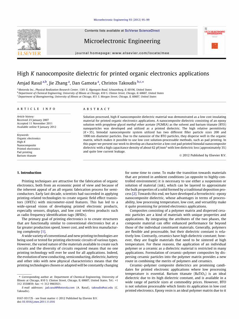
Curing behavior of the nanocomposite was investigated using adifferential scanning calorimeter (DSC, Model 2200 from TA Instru-ments). After curing, the glass transition temperature (Tg) wasmeasured using DSC under modulated mode. The curing profilewith the 60 v% filler is shown in Fig. 6. The cure reaction stars atabout 65 �C and the curing peak appeared at approximately
Nanocomposite Dielectric Viscosity20 hrs after mixing
0.001.002.003.004.005.006.007.008.00
0.00 5.00 10.00 15.00 20.00 25.00Shear Stress
Visc
ocity
, Pas
Shear
Viscocity
Fig. 5. Nanocomposite dielectric viscosity 20 h after mixing.
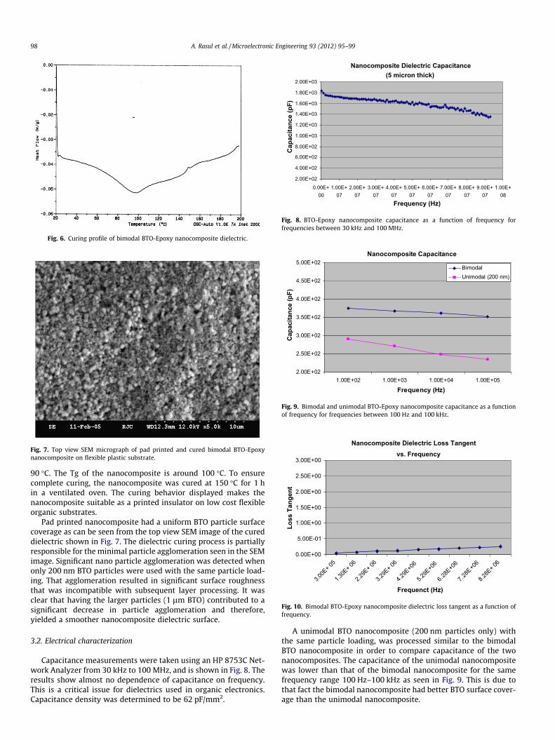
Fig. 6. Curing profile of bimodal BTO-Epoxy nanocomposite dielectric.
Fig. 7. Top view SEM micrograph of pad printed and cured bimodal BTO-Epoxynanocomposite on flexible plastic substrate.
Nanocomposite Dielectric Capacitance(5 micron thick)
2.00E+02
4.00E+02
6.00E+02
8.00E+02
1.00E+03
1.20E+03
1.40E+03
1.60E+03
1.80E+03
2.00E+03
0.00E+00
1.00E+07
2.00E+07
3.00E+07
4.00E+07
5.00E+07
6.00E+07
7.00E+07
8.00E+07
9.00E+07
1.00E+08
Frequency (Hz)
Cap
acita
nce
(pF)
Fig. 8. BTO-Epoxy nanocomposite capacitance as a function of frequency forfrequencies between 30 kHz and 100 MHz.
Nanocomposite Capacitance
2.00E+02
2.50E+02
3.00E+02
3.50E+02
4.00E+02
4.50E+02
5.00E+02
1.00E+02 1.00E+03 1.00E+04 1.00E+05
Frequency (Hz)
Capa
cita
nce
(pF)
BimodalUnimodal (200 nm)
Fig. 9. Bimodal and unimodal BTO-Epoxy nanocomposite capacitance as a functionof frequency for frequencies between 100 Hz and 100 kHz.
Nanocomposite Dielectric Loss Tangentvs. Frequency
0.00E+00
5.00E-01
1.00E+00
1.50E+00
2.00E+00
2.50E+00
3.00E+00
3.00E
+ 05
1.30E
+ 06
2.29E
+ 06
3.29E
+ 06
4.29E
+06
5.29E
+06
6.28E
+06
7.28E
+06
8.28E
+ 06
Frequenct (Hz)
Loss
Tan
gent
Fig. 10. Bimodal BTO-Epoxy nanocomposite dielectric loss tangent as a function offrequency.
98 A. Rasul et al. / Microelectronic Engineering 93 (2012) 95–99
90 �C. The Tg of the nanocomposite is around 100 �C. To ensurecomplete curing, the nanocomposite was cured at 150 �C for 1 hin a ventilated oven. The curing behavior displayed makes thenanocomposite suitable as a printed insulator on low cost flexibleorganic substrates.
Pad printed nanocomposite had a uniform BTO particle surfacecoverage as can be seen from the top view SEM image of the cureddielectric shown in Fig. 7. The dielectric curing process is partiallyresponsible for the minimal particle agglomeration seen in the SEMimage. Significant nano particle agglomeration was detected whenonly 200 nm BTO particles were used with the same particle load-ing. That agglomeration resulted in significant surface roughnessthat was incompatible with subsequent layer processing. It wasclear that having the larger particles (1 lm BTO) contributed to asignificant decrease in particle agglomeration and therefore,yielded a smoother nanocomposite dielectric surface.
3.2. Electrical characterization
Capacitance measurements were taken using an HP 8753C Net-work Analyzer from 30 kHz to 100 MHz, and is shown in Fig. 8. Theresults show almost no dependence of capacitance on frequency.This is a critical issue for dielectrics used in organic electronics.Capacitance density was determined to be 62 pF/mm2.
A unimodal BTO nanocomposite (200 nm particles only) withthe same particle loading, was processed similar to the bimodalBTO nanocomposite in order to compare capacitance of the twonanocomposites. The capacitance of the unimodal nanocompositewas lower than that of the bimodal nanocomposite for the samefrequency range 100 Hz–100 kHz as seen in Fig. 9. This is due tothat fact the bimodal nanocomposite had better BTO surface cover-age than the unimodal nanocomposite.
A. Rasul et al. / Microelectronic Engineering 93 (2012) 95–99 99
Dielectric constant value was calculated from the capacitancedata using Eq. (1):
C ¼ e0erAt
ð1Þ
where, e0 is dielectric constant of the free space (8.85 � 10�12 F/m),A is the area of the electrical conductor plate (30 mm2), t is thethickness of the insulating layer (five micrometer), and er is thedielectric constant of the nanocomposite insulator layer. The nano-composite dielectric constant was calculated to be 35. The nano-composite exhibited a low loss tangent as seen in Fig. 10. The losstangent (tan d) was only 3.2% at 30 kHz. The BTO-Epoxy nanocom-posite dielectric had a breakdown voltage of 23 kV/mm at 1000 Hz.
4. Conclusion
We have developed a promising low temperature, low cost ap-proach to process high capacitance BTO-Epoxy nanocompositedielectric thin films for printed electronics applications. It has beendemonstrated that the pad printing technology can be utilized toprocess thin film dielectric insulators of the nanocomposite. Ther-mal and electrical properties of the nanocomposite dielectric arecompatible with flexible plastic materials. The high capacitancedensity obtained suggests that the BTO-Epoxy nanocompositecan be utilized to reduce the operating voltage of printed electronicdevices.
Acknowledgments
We are grateful to the Motorola Physical Realization ResearchCoE (PRRC) staff and for their contributions. We thank Paul Brazisfor assistance with electrical characterization. We are also gratefulto Huntsman Advanced Materials for their help with formulatingthe nanocomposite material.
References
[1] D. Gamota, P. Brazis, K. Kalyanasundaram, J. Zhang, Printed Organic andMolecular Electronics, Kluwer Academic Publishers, New York, 2004. pp. 161–192.
[2] C. Keimel, J. Gu, S. Chou, Nature 417 (2002) 835–837.[3] S. Ramesh, B. Shutzberg, C. Huang, J. Gao, E. Giannelis, IEEE Trans. Adv. Pack. 26
(2003) 17–24.[4] Y. Rao, K. Tang, and C. Wong, Proceedings of 53rd Electronic Components and
Technology Conference, 2003, 1820–1821.[5] Y. Rao, S. Ogitani, P. Kohl, C. Wong, J. Appl. Poly. Sci. 83 (2002) 1084–1090.[6] Y. Rao, J. Que, T. Marinis, C. Wong, IEEE Trans. Comp. Pack. Tech. A 23 (2002)
680–683.[7] S. Ogitani, S. Bidstrup-Allen, P. Kohl, Comp. Pack. Manu. Tech. B 23 (2000) 313–
322.[8] D. Arlt, J. Appl. Phys. 58 (1985) 1619–1622.[9] K. Uchino, E. Sadanaga, T. Hirose, J. Am. Ceram. Soc. 72 (1989) 1555–1562.
[10] S. Cho, J. Lee, J. Hyun, K. Paik, Mater. Sci. Eng. B 110 (2004) 233–239.[11] B. Shutzberg, C. Huang, S. Ramesh, and E. Giannelis, Proceedings of 50th
Electronic Components and Technology Conference, 1568–1571.[12] M. Bohan, T. Claypole, A. Clist, D. Gethin, TAGA Journal of Graphic Technology
110 (2001) 1–12.