hexagon dsp:an architecture mobile...
TRANSCRIPT
.................................................................................................................................................................................................................
HEXAGON DSP: AN ARCHITECTUREOPTIMIZED FOR MOBILE MULTIMEDIA
AND COMMUNICATIONS.................................................................................................................................................................................................................
THE QUALCOMM HEXAGON DSP IS USED FOR BOTH MODEM PROCESSING AND
MULTIMEDIA ACCELERATION. BY OFFLOADING MULTIMEDIA TASKS FROM THE CPU TO THE
DSP, SIGNIFICANT POWER SAVINGS CAN BE ACHIEVED. THIS ARTICLE PROVIDES AN
OVERVIEW OF THE HEXAGON ARCHITECTURE. THE PROCESSOR IS DESIGNED TO DELIVER
SUPERIOR ENERGY EFFICIENCY COMPARED TO MOBILE CPU ALTERNATIVES AND THEREBY
HELP ACHIEVE LONG BATTERY LIFE FOR IMPORTANT MOBILE APPLICATIONS.
......To be competitive, a modernmobile product must provide a rich user expe-rience and long battery life. Chips for theseecosystems integrate multiple subsystems,each customized for a particular applicationdomain. By specializing a subsystem to a task,performance and power can be enhancedbeyond what is possible with a homogenousCPU-based computing platform.
Figure 1 shows a block diagram of theSnapdragon 800. This chip contains dedicatedsubsystems for camera, display, video, audio/voice, sensors, graphics, cellular modem, Wi-Fi, and more. Each subsystem contains dedi-cated hardware, and many contain special-purpose processing engines and software cus-tomized to the task.
The Snapdragon 800 has two instances ofthe Hexagon digital-signal processor (DSP).The modem (mDSP) is dedicated andcustomized for modem processing, whereasthe application DSP (aDSP) is used for mul-timedia acceleration. The modem processoris a closed subsystem and is programmedonly within Qualcomm Technologies. The
multimedia DSP, however, is licensed forprogramming by OEMs and third-party soft-ware vendors. This article provides an over-view of the multimedia DSP and builds onthe presentation from HotChips 25.1
Figure 2 shows the various Hexagon gen-erations. Version 2 (V2) was the first pro-duction version and appeared in the initialSnapdragon mobile products in 2007. V3featured an improved implementation withbetter power consumption. These early ver-sions of Hexagon targeted voice and audioprocessing. Example functions include wide-band vocoders, echo cancellation, audiopostprocessing filters, MP3/AAC play-back, speaker protection algorithms, andso on.
V4 and V5 expanded the application tar-gets to include image processing for cameraand video; computer vision tasks such ashand, gesture, and face recognition; andprocessing of sensor input (gyro, accelerome-ter, fingerprint, and so on). Unless otherwisenoted, this article will focus on the latestHexagon V5 core.
Lucian Codrescu
Willie Anderson
Suresh Venkumanhanti
Mao Zeng
Erich Plondke
Chris Koob
Ajay Ingle
Charles Tabony
Rick Maule
Qualcomm
.......................................................
34 Published by the IEEE Computer Society 0272-1732/14/$31.00�c 2014 IEEE

• aDSP: Real-timemedia & sensorprocessing
Camera KraitAdreno
Krait
Snapdragon800
Audio
Display
JPEG
Video
CPUAdrenoGPU
KraitCPU
CPU
KraitCPU
Misc.connectivity
HexagonaDSP
Sensors
Other
Multimedia fabric System fabric
2-Mbyte L2
ModemFabric & memory controllerHexagon
mDSP
LPDDR3 LPDDR3• mDSP: Dedicated
modem processing
Figure 1. Snapdragon 800 block diagram. The chip contains dedicated subsystems for camera, display, video, audio/voice,
sensors, graphics, cellular modem, and Wi-Fi.
V3 mDSP45 nm
June 2009
V4 mDSP28 nm
Dec. 2010
V5 mDSP28 nm
Dec. 2012
V4 aDSPLow-tier28 nm
Apr. 2011V2 aDSP
65 nmDec. 2007
V3 aDSPLow-tier45 nm
Nov. 2009
V1 aDSP65 nm
Oct. 2006
V3 aDSP45 nm
Aug. 2009
V4 aDSP28 nm
Dec. 2010
V5 aDSP28 nm
Dec. 2012
Time
Figure 2. Hexagon digital-signal processor (DSP) evolution. The figure shows the evolution from Version 1 in October 2006
through Version 5 in December 2012.
.............................................................
MARCH/APRIL 2014 35
Hexagon is a multithreaded very longinstruction word (VLIW) DSP. The designphilosophy is to maximize work per cycle forperformance, but target the microarchitec-ture to modest clock speeds and low power.
Instruction-set architecture overviewThe architecture’s foundation is a stati-
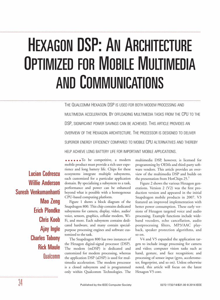
cally scheduled four-way VLIW. The VLIWapproach puts the burden of instruction par-allelism on the compiler and thereby avoidscostly and power-hungry dynamic-schedulinghardware.2 The VLIW approach is popularamong commercial DSPs. Figure 3 shows ablock diagram of Hexagon.
Registers and memoryThe Hexagon processor features a unified
byte-addressable memory. This memory hasa single 32-bit virtual address space that holdsboth instructions and data. It operates inlittle-endian mode. A full-featured memorymanagement unit (MMU) translates virtualto physical addresses.
All user-level registers are replicated perthread. There are two sets of user registers:general registers and control registers. Thegeneral registers include thirty-two 32-bitregisters that can be accessed either as singleregisters or as aligned 64-bit register pairs.The general registers contain all pointer, sca-lar, vector, and accumulator data. The con-trol registers include special-purpose registerssuch as the program counter, status register,and loop registers.
Data-processing instructionsThere are two identical 64-bit single-
instruction, multiple-data (SIMD) executionunits. Each unit supports all multiply, shift,arithmetic logic unit (ALU), and bit manipu-lation instructions. Supported data typesinclude
� 8-, 16-, 32-, and 64-bit integer;� 16- and 32-bit fractional with optional
rounding and saturation;� 16-bit complex; and� single-precision IEEE-compatible float-
ing point.
Each unit is capable of supporting:
� four 16� 16 multiplies;� two 32� 16 multiplies; or� one 32 � 32 multiply, one complex
multiply, or one floating-point fusedmultiply-add (FMA).
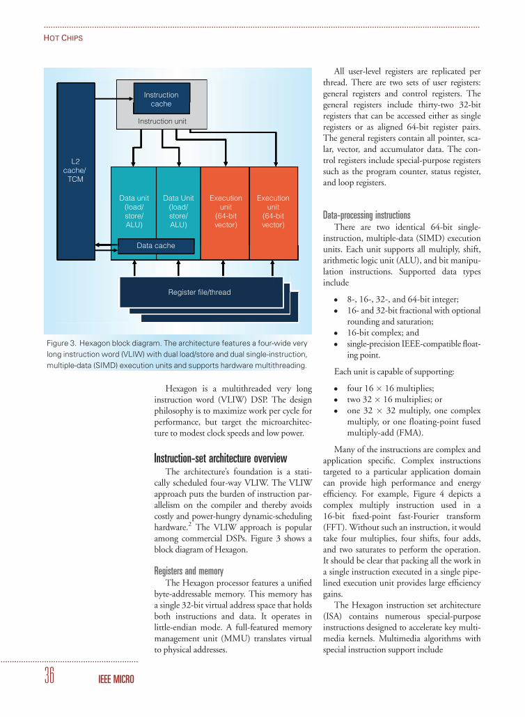
Many of the instructions are complex andapplication specific. Complex instructionstargeted to a particular application domaincan provide high performance and energyefficiency. For example, Figure 4 depicts acomplex multiply instruction used in a16-bit fixed-point fast-Fourier transform(FFT). Without such an instruction, it wouldtake four multiplies, four shifts, four adds,and two saturates to perform the operation.It should be clear that packing all the work ina single instruction executed in a single pipe-lined execution unit provides large efficiencygains.
The Hexagon instruction set architecture(ISA) contains numerous special-purposeinstructions designed to accelerate key multi-media kernels. Multimedia algorithms withspecial instruction support include
Instruction unit
L2cache/
TCM
Data unit(load/store/ALU)
Data Unit(load/store/ALU)
Executionunit
(64-bitvector)
Executionunit
(64-bitvector)
Data cache
Register file/thread
Instructioncache
Figure 3. Hexagon block diagram. The architecture features a four-wide very
long instruction word (VLIW) with dual load/store and dual single-instruction,
multiple-data (SIMD) execution units and supports hardware multithreading.
..............................................................................................................................................................................................
HOT CHIPS
............................................................
36 IEEE MICRO
� variable-length encode/decode, suchas context-adaptive binary-arithmetic-coding processing in H.264 video;
� features from accelerated segmenttest (FAST) corner detection imageprocessing;
� FFTalgorithms;� sliding-window filters;� linear-feedback shift;� table lookup from an arbitrary bit
field index;� elliptic curve cryptography; and� cyclic redundancy check (CRC)
calculation.
Load/store instructionsDual load/store units access signed or
unsigned 8-, 16-, 32-, and 64-bit values inmemory. There is a rich variety of addressingmodes, including
� absolute 32-bit,� base plus scaled immediate and base
plus scaled register,� auto-incrementing by register and
immediate,� circular addressing, and� bit reversed.
To increase the number of instructioncombinations allowed in packets, the load/store units also support 32-bit ALUinstructions.
Conditional execution and program flowThe Hexagon ISA includes conditional
execution. Conditional execution is useful toremove branches through if-conversion andis helpful for a VLIW processor. Compareinstructions target one of four predicate regis-ters. These predicate registers can then beused to conditionally execute certain instruc-tions. Not all instructions can be condi-tional—only the most common load/storeand ALU instructions.
A unique feature of Hexagon conditionalexecution is that the processor can generateand use a predicate in the same VLIW in-struction packet. This reduces packet countand creates denser packets, both of whichimprove performance and reduce energy con-sumption. Consider the following C state-ment and the corresponding assembly code
that is generated from it by the compiler. The“.new” suffix implies the source predicate isgenerated in the same packet. In this exam-ple, the dot-new construct enables the workto be done in one instruction packet insteadof two.
The C statement is as follows:if (R2 == 4)
R3 = *R4;
else
R5 = 5;
Assembly code with braces delineatepacket boundaries:{
P0 = cmp.eq(R2,#4)
if (P0.new) R3 = memw(R4)
if (!P0.new) R5 = #5
}
Similar to many DSP processors, Hexa-gon includes a zero-overhead hardwarecounted looping mechanism with supportfor two levels of nesting. An instruction isused to initialize the loop count and the startaddress. Bits encoded in the last packet of theloop delineate the end of the loop. Thisarchitecture allows execution of loops with
Rs R
R
32 32 32
Add Add
Sat_32Sat_32
High 16bitsHigh 16bits
RdRI
32
0x80000x8000 <<0–1<<0–1
–
<<0–1<<0–1
∗ ∗ ∗ ∗
R
RRt
Rs
RtI
I
I
I
Figure 4. Complex multiply instruction. Such an instruction executed in a
single pipelined execution unit provides large efficiency gains for
applications that use complex arithmetic.
.............................................................
MARCH/APRIL 2014 37

no branch mispredicts or stalls, and no hard-ware devoted to loop branch prediction.
Compound and memop instructionsCompound instructions combine two or
more dependent operations in a single instruc-tion. These instructions improve code size andsave power by reducing register file and for-warding power. Hexagon includes many suchinstructions, including shift-add, shift-or, add-add, compare-branch, shift-xor, and many fla-vors of the classic DSP multiply-add.
Another class of instruction performs sim-ple operations directly on memory, includingadd, subtract, logical–or, and logical–and.Without these memory operations (mem-ops), three instructions would be necessary toperform the same task: one to load the value,one to perform the arithmetic or logical oper-ation on the value, and one to store the result.Memops improve code size and reduce powerbecause intermediate register access is notneeded.
VLIW instruction groupingVLIW instruction packets are variable
sized and contain one to four instructions. Ifa packet contains more than one instruction,the instructions execute in parallel. Theinstruction combinations allowed in a packetare limited to the instruction types that canbe executed in parallel in the four executionunits. The processor uses parallel executionsemantics. All registers are read, then allinstructions are executed, then all registersare written.
Duplex instructionsLow code size is advantageous for an
embedded processor. Hexagon instructionsare fixed size and 32 bits in length. Toimprove code size, the Duplex feature enablessome use of 16-bit instructions by creating a32-bit subpacket containing two 16-bitinstructions. These subpackets are calledduplexes. Figure 5 shows a visualization of aduplex.
Because duplexes are always 32 bits,packet sizes continue to be multiples of 32bits. This leads to a simpler and lower-powerimplementation as compared to instructionsets with a mixed 16-/32-bit instruction set.Additionally, duplexes must always end apacket, and are always dispatched to the sametwo execution units, which further simplifiesthe implementation. The instructions allowedin duplexes, called subinstructions, are the mostcommon subset of normal Hexagon instruc-tions, with reduced ranges of registers andimmediate operands.
Multithreading and microarchitectureThe Hexagon processor is multithreaded.
The number of threads varies by implemen-tation. Early implementations included sixhardware threads, but more recent coresinclude three hardware threads. There aremany trade-offs in choosing the number ofthreads. Additional threads provide morelatency tolerance and enable power-savingopportunities in the microarchitecture byserializing work rather than speculatingwork. On the other hand, additional threadsincrease cache pressure and increase the soft-ware programming burden. Our experienceis that three or four threads are a sweet spotin the design space.
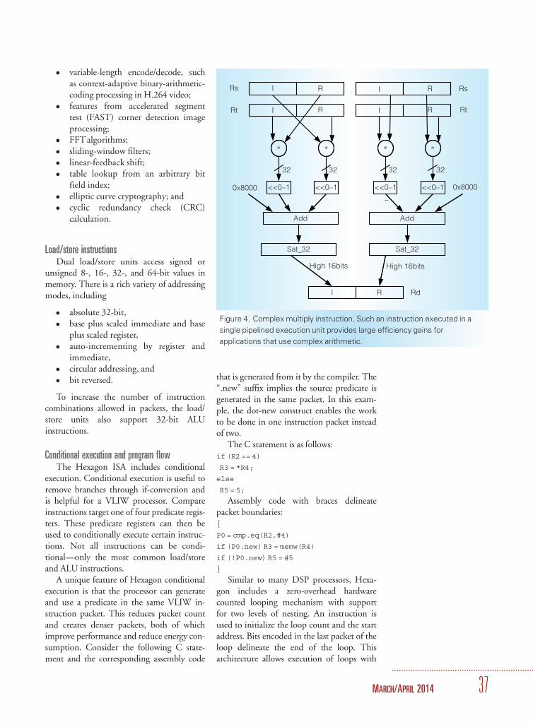
Hexagon is designed to look like a multi-core architecture with communicationthrough shared memory. Figure 6 shows howthe processor appears to the programmer.Software threads are mapped to hardwarethreads by the operating system.
In the physical implementation, however,there is only one processor, which the threehardware threads share. Hexagon V1 throughV4 implemented a simple round-robin inter-leaved multithreading (IMT) approach.3 Onevery clock tick, a different thread is given a
Each box is an instruction.
Packet of four 32-bit instructions
Packet of two 32-bit instructions and a duplex
32 bits
32 bits
32 bits
32 bits
32 bits
32 bits
16 bits 16 bits
Figure 5. Visualization of a duplex. A duplex
is a 32-bit subpacket containing two 16-bit
instructions.
..............................................................................................................................................................................................
HOT CHIPS
............................................................
38 IEEE MICRO
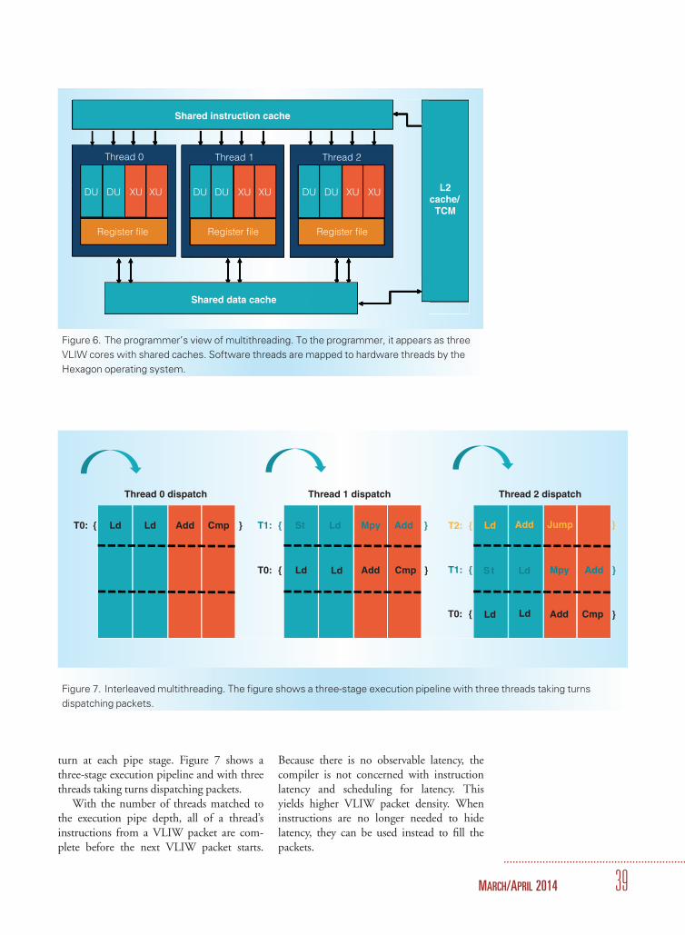
turn at each pipe stage. Figure 7 shows athree-stage execution pipeline and with threethreads taking turns dispatching packets.
With the number of threads matched tothe execution pipe depth, all of a thread’sinstructions from a VLIW packet are com-plete before the next VLIW packet starts.
Because there is no observable latency, thecompiler is not concerned with instructionlatency and scheduling for latency. Thisyields higher VLIW packet density. Wheninstructions are no longer needed to hidelatency, they can be used instead to fill thepackets.
Thread 0 Thread 1 Thread 2
Shared instruction cache
DU DU L2cache/ TCM
XU DU XUDU XU
Register file Register file Register file
Shared data cache
DU DU XUXU XU
Figure 6. The programmer’s view of multithreading. To the programmer, it appears as three
VLIW cores with shared caches. Software threads are mapped to hardware threads by the
Hexagon operating system.
Thread 0 dispatch Thread 1 dispatch Thread 2 dispatch
T0: { Ld Ld Add Cmp } T1: { St Ld Mpy Add }
T0: { Ld Ld Add Cmp }
T2: { Ld
Add Jump }
T1: { St Ld
Mpy
Add }
T0: { Ld
Ld
Add Cmp
}
Figure 7. Interleaved multithreading. The figure shows a three-stage execution pipeline with three threads taking turns
dispatching packets.
.............................................................
MARCH/APRIL 2014 39
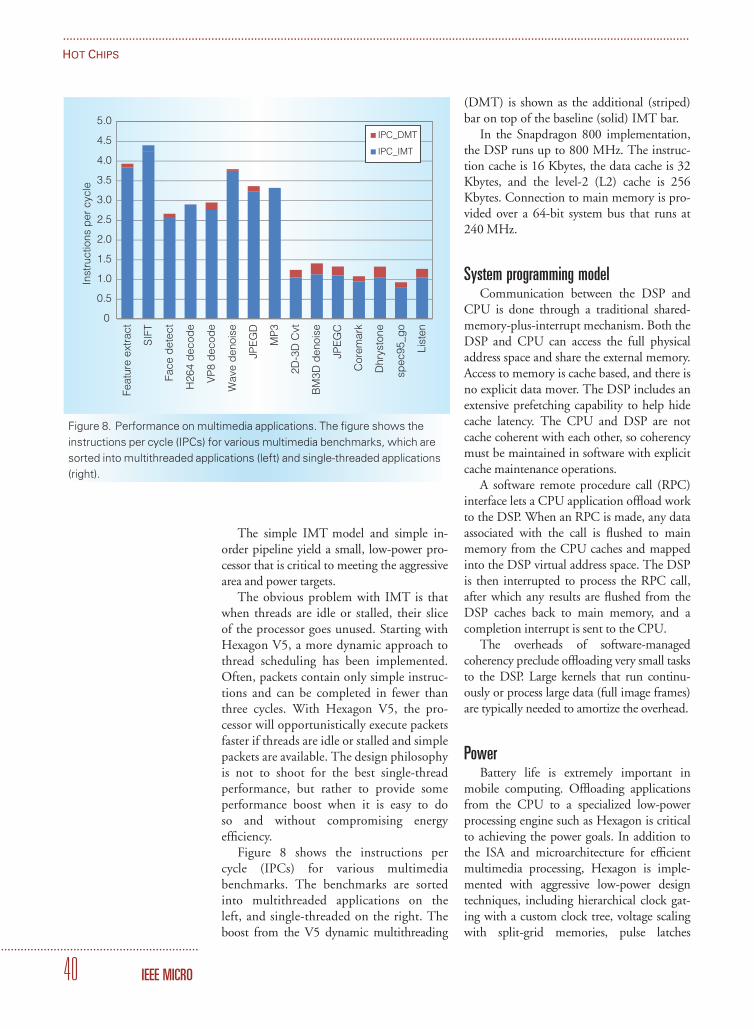
The simple IMT model and simple in-order pipeline yield a small, low-power pro-cessor that is critical to meeting the aggressivearea and power targets.
The obvious problem with IMT is thatwhen threads are idle or stalled, their sliceof the processor goes unused. Starting withHexagon V5, a more dynamic approach tothread scheduling has been implemented.Often, packets contain only simple instruc-tions and can be completed in fewer thanthree cycles. With Hexagon V5, the pro-cessor will opportunistically execute packetsfaster if threads are idle or stalled and simplepackets are available. The design philosophyis not to shoot for the best single-threadperformance, but rather to provide someperformance boost when it is easy to doso and without compromising energyefficiency.
Figure 8 shows the instructions percycle (IPCs) for various multimediabenchmarks. The benchmarks are sortedinto multithreaded applications on theleft, and single-threaded on the right. Theboost from the V5 dynamic multithreading
(DMT) is shown as the additional (striped)bar on top of the baseline (solid) IMT bar.
In the Snapdragon 800 implementation,the DSP runs up to 800 MHz. The instruc-tion cache is 16 Kbytes, the data cache is 32Kbytes, and the level-2 (L2) cache is 256Kbytes. Connection to main memory is pro-vided over a 64-bit system bus that runs at240 MHz.
System programming modelCommunication between the DSP and
CPU is done through a traditional shared-memory-plus-interrupt mechanism. Both theDSP and CPU can access the full physicaladdress space and share the external memory.Access to memory is cache based, and there isno explicit data mover. The DSP includes anextensive prefetching capability to help hidecache latency. The CPU and DSP are notcache coherent with each other, so coherencymust be maintained in software with explicitcache maintenance operations.
A software remote procedure call (RPC)interface lets a CPU application offload workto the DSP. When an RPC is made, any dataassociated with the call is flushed to mainmemory from the CPU caches and mappedinto the DSP virtual address space. The DSPis then interrupted to process the RPC call,after which any results are flushed from theDSP caches back to main memory, and acompletion interrupt is sent to the CPU.
The overheads of software-managedcoherency preclude offloading very small tasksto the DSP. Large kernels that run continu-ously or process large data (full image frames)are typically needed to amortize the overhead.
PowerBattery life is extremely important in
mobile computing. Offloading applicationsfrom the CPU to a specialized low-powerprocessing engine such as Hexagon is criticalto achieving the power goals. In addition tothe ISA and microarchitecture for efficientmultimedia processing, Hexagon is imple-mented with aggressive low-power designtechniques, including hierarchical clock gat-ing with a custom clock tree, voltage scalingwith split-grid memories, pulse latches
4.5
5.0
0
0.5
1.0
1.5
2.0
2.5
3.0
3.5
4.0
Feat
ure
extr
act
SIF
T
Face
det
ect
H26
4 d
ecod
e
VP
8 d
ecod
e
Wav
e d
enoi
se
JPE
GD
MP
3
2D-3
D C
vt
BM
3D d
enoi
se
JPE
GC
Cor
emar
k
Dhr
ysto
ne
spec
95_g
o
List
en
Inst
ruct
ions
per
cyc
le
IPC_DMT
IPC_IMT
Figure 8. Performance on multimedia applications. The figure shows the
instructions per cycle (IPCs) for various multimedia benchmarks, which are
sorted into multithreaded applications (left) and single-threaded applications
(right).
..............................................................................................................................................................................................
HOT CHIPS
............................................................
40 IEEE MICRO
instead of flip-flops, and full-custom cachesand register files designed for low power. Amore complete description of the low-powertechniques used by Hexagon is availableelsewhere.4
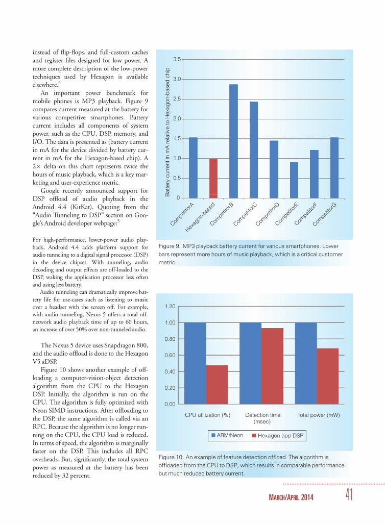
An important power benchmark formobile phones is MP3 playback. Figure 9compares current measured at the battery forvarious competitive smartphones. Batterycurrent includes all components of systempower, such as the CPU, DSP, memory, andI/O. The data is presented as (battery currentin mA for the device divided by battery cur-rent in mA for the Hexagon-based chip). A2� delta on this chart represents twice thehours of music playback, which is a key mar-keting and user-experience metric.
Google recently announced support forDSP offload of audio playback in theAndroid 4.4 (KitKat). Quoting from the“Audio Tunneling to DSP” section on Goo-gle’s Android developer webpage:5
For high-performance, lower-power audio play-back, Android 4.4 adds platform support foraudio tunneling to a digital signal processor (DSP)in the device chipset. With tunneling, audiodecoding and output effects are off-loaded to theDSP, waking the application processor less oftenand using less battery.
Audio tunneling can dramatically improve bat-tery life for use-cases such as listening to musicover a headset with the screen off. For example,with audio tunneling, Nexus 5 offers a total off-network audio playback time of up to 60 hours,an increase of over 50% over non-tunneled audio.
The Nexus 5 device uses Snapdragon 800,and the audio offload is done to the HexagonV5 aDSP.
Figure 10 shows another example of off-loading a computer-vision-object detectionalgorithm from the CPU to the HexagonDSP. Initially, the algorithm is run on theCPU. The algorithm is fully optimized withNeon SIMD instructions. After offloading tothe DSP, the same algorithm is called via anRPC. Because the algorithm is no longer run-ning on the CPU, the CPU load is reduced.In terms of speed, the algorithm is marginallyfaster on the DSP. This includes all RPCoverheads. But, significantly, the total systempower as measured at the battery has beenreduced by 32 percent.
3.0
3.5
2.0
2.5
1.0
1.5
0.5
Competi
torA
Competi
torB
Competi
torC
Competi
torD
Competi
torE
Competi
torF
Competi
torG
Hexag
on-b
ased
Bat
tery
cur
rent
in m
A r
elat
ive
to H
exag
on-b
ased
chi
p
0
Figure 9. MP3 playback battery current for various smartphones. Lower
bars represent more hours of music playback, which is a critical customer
metric.
1.00
1.20
0.00
0.20
0.40
0.60
0.80
CPU utilization (%) Detection time(msec)
Total power (mW)
ARM/Neon Hexagon app DSP
Figure 10. An example of feature detection offload. The algorithm is
offloaded from the CPU to DSP, which results in comparable performance
but much reduced battery current.
.............................................................
MARCH/APRIL 2014 41

Figure 11 provides additional examples ofperformance and power, comparing the Hex-agon V5 DSP to the CPU used in the Snap-dragon 200 chip. Each chart features adifferent algorithm used in a computer visionapplication. For the CPU, all code is fullyoptimized using Neon SIMD instructions.Both single-CPU and quad-CPU data isshown. The x-axis shows latency in units oftime/pixel, and the y-axis shows energy/pixel.The origin is (0,0) in all charts. Power ismeasured at the battery and includes all sys-tem power. When compared to the quadCPU in Snapdragon 200, the Hexagon V5DSP provides similar or better performanceand lower power in all cases.
T his article provides an overview of theHexagon DSP architecture. The
demand for low-power signal processing inmobile applications continues unabated.Camera and video applications requiresophisticated signal processing at ultra-highdefinition resolution. At the same time,“always-on” voice activation features arepushing power requirements to new lows.Future versions of Hexagon DSP will beenhanced and specialized to tackle theseupcoming challenges.
For readers who would like to explorefurther, the Hexagon Software Developer’sKit (https://developer.qualcomm.com/mobile-development/maximize-hardware/multimedia-optimization-hexagon-sdk/multimedia-optimization-h-2) provides everythingneeded to program the DSP, includingfull documentation, software tools, acycle-approximate simulator, and examplecode. MICRO
....................................................................References1. L. Codrescu et al., “Qualcomm Hexagon
DSP: An Architecture Optimized for Mobile
Multimedia and Communications,” Hot
Chips 25, 2013.
2. J. Fisher, “VLIW Architectures: An Inevita-
ble Standard for the Future?” J. Supercom-
puter, vol. 7, no. 2, 1990, pp. 29-36.
3. B. Smith, “Architecture and Applications of
the HEP Multiprocessor Computer Sys-
tem,” SPIE Real Time Signal Processing IV,
1981, pp. 241-248.
4. M. Saint-Laurent et al., “A 28 nm DSP Pow-
ered by an On-Chip LDO for High-Per-
formance and Energy-Efficient Mobile
Applications,” to be published in Proc. IEEE
Int’l Solid-State Circuits Conf., 2014.
Canny
Time/pixel(nSec)
Ene
rgy/
pix
el(n
J)
Fast9
Time/pixel(nSec)
Ene
rgy/
pix
el(n
J)
Intensity histogram
Time/pixel(nSec)
Ene
rgy/
pix
el(n
J)
Harris
Time/pixel(nSec)
Ene
rgy/
pix
el(n
J)
NCC
Time/pixel(nSec)
Ene
rgy/
pix
el(n
J)
- CPUx1 CPU @ 1.2 GHz - CPUx4 - DSP DSP @ 690 MHz
Figure 11. Energy versus latency for multimedia benchmarks. Each chart features a different algorithm used in a computer
vision application.
..............................................................................................................................................................................................
HOT CHIPS
............................................................
42 IEEE MICRO

5. “Android KitKat: New Media Capabilities,”
Android.com, Jan. 2014, http://developer.
android.com/about/versions/kitkat.html#44-
media.
Lucian Codrescu is a senior director atQualcomm, where he leads the HexagonArchitecture team. Codrescu has a PhD incomputer engineering from the GeorgiaInstitute of Technology.
Willie Anderson is a vice president at Qual-comm, where he runs the DSP engineeringorganization. Anderson has a BS in physicsfrom the University of Texas at Austin.
Suresh Venkumanhanti is a principal engi-neer at Qualcomm, where he is responsiblefor the DSP core microarchitecture. Venku-manhanti has an MS in electrical engineer-ing from the University of Florida.
Mao Zeng is a senior staff engineer at Qual-comm and a principal designer of the DSPinstruction set architecture. Zeng has a PhDin electrical engineering from the Universityof Victoria.
Erich Plondke is a senior staff engineer atQualcomm, where he leads the systemarchitecture team. Plondke has an MS inelectrical engineering from the GeorgiaInstitute of Technology.
Chris Koob is a principal engineer at Qual-comm, where he is responsible for the memorysystem microarchitecture. Koob has an MS inelectrical engineering from Virginia Tech.
Ajay Ingle is a principal engineer at Qual-comm, where he is responsible for DSParchitecture support of modem applications.Ingle has an MS in electrical engineeringfrom Texas A&M University.
Charles Tabony is a senior engineer atQualcomm, where he contributes to theinstruction set design and performance veri-fication. Tabony has a BS in computer engi-neering from the University of Texas.
Rick Maule is a senior director at Qual-comm, where he is responsible for DSPproduct management. Maule has an MS inelectrical engineering from the University ofArkansas.
Direct questions and comments about thisarticle to Lucian Codrescu at [email protected].
.............................................................
MARCH/APRIL 2014 43