functional tolerancing using full surface metrology tolerancing using...with the shrinkage of...
TRANSCRIPT

Functional tolerancing using full surface metrology Robert D. Grejda*, Katherine Ballman, Chris A. Lee
Corning Tropel Corporation, 60 O’Connor Road, Fairport NY 14450
ABSTRACT
This paper highlights two examples of the use of full surface metrology to allow for functional tolerancing of components in the areas of EUV lithography (reticle characterization) and DUV precision lens manufacturing (lens holder metrology). For both examples, the measurement of the full surface is a key enabler to understanding the critical characteristics to control and tolerance for functionality or performance. Interferometric techniques are used to provide high resolution and accurate measurements for both examples. Subsequently, this data can be used to identify the surface characteristics that contribute to the end functionality and provide a means for deterministic correction or compensation.
Keywords: flatness, functional tolerances, EUV, reticle, opto-mechanics, interferometry, full surface metrology, low-stress mounting
1. INTRODUCTION For the past several decades, the lithographic industry has met the call of Moore’s Law through increasingly clever process improvements. With the shrinkage of feature sizes, tolerances around specifications were tightened to ensure accuracy, and although these specifications were often complex and challenging, the industry rose to the challenge. Through many years and iterations of this process, feature shrinkage and tolerance tightening, higher cost became obvious to bystanders. As in most industries, in order to improve the key attributes of high performance products, tighter and tighter process controls were required. The specific drivers for different applications may differ, but the resulting trend is that improved manufacturing capability and process controls result in a competitively advantaged product. The simplest and often first approach to achieve these advantages is simply to reduce all of the blanket tolerance windows.
In this paper, we present two applications of functional tolerances as a method to achieve high performance specifications in which traditional blanket tolerances loosen in favor of embracing a “root cause” approach to device performance. Functional tolerances allow us to ensure the overall system specifications are achieved through thoughtful analysis and engineering at the component level. This method utilizes surface information to drive down error contributors rather than just tightening specifications to drive components to “near perfection” at the expense of cost and throughput.
The first application uses an in depth knowledge of the complete system architecture combined with full surface flatness measurements from the surface of an EUV reticle and showcases potential for overlay error mitigation through compensation schemes as opposed to total surface tolerances requiring performance at the edge of the viable process capability. The second application shows the use of full surface interferometric measurements of optical element holders (cells) and uses the data, along with understanding of the assembly process to decrease stress and strain introduced during system assembly. For both examples, the intention is to shift process complexity to a singular one-time engineering cost rather than tightening blanket specifications and pushing higher cost onto each component manufactured for every single system. The nature of full surface measurements is that the components are characterized with great detail, enabling the capability to draw correlations of the component shape to the resulting system or process.
*[email protected]; phone 1 585 388-3494; www.corning.com/worldwide/en/products/advanced-optics.html

2. EUV PHOTOMASK FLATNESS OVERLAY ERROR MITIGATION As feature sizes have decreased, tolerances around image placement have decreased as well, and factors contributing to image placement error have faced increased scrutiny. EUV photomasks in particular have faced a very significant tightening of their geometric tolerances and are now facing single digit nanometer flatness specifications. Shifting from the on-axis illumination of the photomask in optical lithography to the reflective imaging of EUV lithography results in a direct relationship between the topography of the photomask on the electrostatic chuck within the EUV scanner and the resulting image placement error at the wafer. In this section, we discuss the key parameters of reticle flatness and their resulting contribution to image placement errors. From these metrics, we then discuss the manufacturing options available to reach the required specifications; tightened GD&T, or functional tolerancing with the adoption of a data based corrective process. The compensation strategies proposed look at the results of the reticles’ full surface flatness measurement, and then analyze the corrective capabilities available within the proposed processes (at scanner or at write) in order to determine the residual error following the implementation of such a process (Figure 1).
Figure 1: Full surface interferometric measurements create the opportunity to conduct a thorough analysis of EUV blank
topographies and simulate the viability of different correction options. [1]
2.1 Image Placement Errors Related to Photomask Flatness
The magnitude of the image placement error related to the photomask’s shape can be characterized from two sets of distortion. In-plane distortion (IPD) results from differences in the chucking mechanisms between reticle patterning and exposure in the scanner. EUV scanners require the use of electrostatic chucking, while reticle patterning tools use more simplistic 3-point chucks for holding the photomask during its exposure. When the patterned mask is then chucked in the scanner, the pattern is shifted through in-plane distortion, which can be calculated as shown below in Figure 2a. The image placement error from IPD can vary depending on the method of calculation [2] and is discussed further in Section 2.3. Out-of-plane distortion (OPD) occurs when the surface of the photomask deviates from its ideal plane within the EUV lithography tool. EUV lithography is reflective in nature, and the illumination of the reticle is at an angle (approximately 6 degrees). Therefore, height variation at the reticle surface results in a corresponding lateral shift of the pattern upon reflection, as can be seen in Figure 2b.

(a) (b)
Figure 2: Schematic demonstrating the image placement errors from both (a) IPD and (b) OPD.
The contributions of OPD and IPD sum to the final image placement error caused by the reticles shape. Both IPD and OPD can be controlled through tightened tolerances on flatness; however the overlay budget for high end nodes allots only a small percentage of its error for flatness and image placement related to flatness. Estimates of these contributions are summarized in Table 1. The system specifications were estimated by using the calculation methods from the last published ITRS [3] in combination with the 2015 NXE technology roadmap [4]. It is important to note that both referenced materials are outdated, and it is likely that the raw specifications (those that don’t implement a holistic correction) could potentially be tighter.
Table 1: Photomask topography strawman budget for 10nm and 7nm resolutions, based on calculations from previous ITRS and NXE roadmap [1].
Node Resolution ITRS+ NXE RoadMap
N5 10nm
Budgeted Overlay (nm) 1.2 Image Placement (nm) 0.7
Flatness (nm) 6.9 Slope (urad) 0.2
N3 7nm
Budgeted Overlay (nm) 1.0 Image Placement (nm) 0.6
Flatness (nm) 5.7 Slope (urad) 0.2
From these estimations, it stands that photomask blanks for 7nm resolution would have to adhere to a flatness specification of roughly 6nm P-V. Although the photomask industry has made incredible strides in the last decade to improve blanks flatness, champion mask performance is typically around 10’s of nm, accompanied by a significant increase in price, and a decrease in throughput. It is for these reasons that we propose the adoption of compensation techniques which would allow current levels of blank flatness to be used, and still meet the ultimate image placement and overlay specifications. In the following sections we discuss which factors require consideration for each compensation technique and compare them to the procedures used to achieve the low level flatness required by GD&T specs, and further discuss the advantages and challenges for each process.

2.2 Manufacturing Methods vs. Functional Tolerances
Standard reticle polishing procedures can yield photomasks with flatness ~150nm [5]. A reticle with this level of non-flatness contributes a significant amount of image placement error during wafer print. The specifications and calculations discussed in the previous section indicate a limit of ~6nm non-flatness to achieve the 7 nm node overlay requirements. To achieve this level of flatness requires the use of conventional polishing techniques, as well as NC local polishing approaches used in iteration with feedback from high accuracy metrology instruments. Figure 3 shows a basic schematic of these iterations using an UltraFlatTM reticle measurement tool as the processes metrology feedback for local polishing.
Figure 3: Flow diagram depicting the process steps for polishing of photomask blanks [5].
A deterministic finishing process starts from a more conventional surface generation, and then using high resolution high accuracy measurement feedback, a process with variable removal rate is used to converge on the final specifications. In a simplistic analysis this can be modeled as a linear system with a convergence rate (slope) and a base error level (intercept). When the requirements approach the limits of convergence, the number of iterations increases with diminishing returns on flatness as shown in Figure 4.
Figure 4: Chart showing the cost to achieve various levels of flatness using deterministic finishing processes.
1
10
100
1000
$- $500 $1,000 $1,500 $2,000 $2,500 $3,000
Flat
ness
(nm
)
Processing Cost
Cost of Flatness
70% + 5
70% + 4
70% + 3
Target N5
Target N3

Figure 4 represents the requirements driving down to the fundamental manufacturing process limits. In addition to the convergence limits of deterministic finishing, there are also local polishing steps at the end of this process to minimize any high spatial frequencies introduced from the deterministic finishing. In Figure 3 above, this is referred to as “Touch Polishing”, and this can improve high and mid spatial content, but typically makes the mid to low frequency figure worse, and with very tight specifications may force the iterative process to start over. Under these circumstances, any type of specification relief not only reduces the per part cost of manufacturing, but becomes a fundamentally enabling technology. These types of situations are the strongest candidates for a deeper look into the functional tolerance requirements, as any form of specification relief can have a dramatic impact on product viability.
With a process limited application such as this, it is highly desirable to dig deeper and understand what drives the tolerances, and see if there is a way to tease apart these requirements and refocus the efforts on improving the critical portions, ultimately loosening up the requirements in the areas that have more process tolerance.
2.3 Full Surface Data Analysis for Holistic Corrections
The adoption of a holistic correction method requires a detailed understanding of each process involved in the ultimate systems performance, and their relative error contributions. The type of analysis needed to determine these factors is thorough, collaborative, and in many cases time consuming, however the advantage over a brute force method for GD&T is that the analysis is done one time over the process, as opposed to having to perform extended efforts (and increasing cost) over every single part. In this section we further discuss some of the error contributors which are considered when evaluating the proposed reticle flatness compensation methods [1].
Figure 5: Fishbone diagram showing items taken into consideration for error calculation and correction process
implementation.
Corrective processes must consider the implications of the scanner environment and include them in their error model. Such consideration including the nature of the electrostatic chuck, as well as the releveling method of the reticle once chucked. Using data collected from full surface interferometric measurements of the reticle, combined with knowledge of the corrective capabilities from each potential holistic application, we are then able to model the resulting error contribution using the equations shown in Section 2.1. Each correction process will have different methods and varying magnitudes of correction, and as such will require different algorithms to estimate their corrective capabilities and residuals. The three corrections shown in Figure 6, linear scanner, high order scanner, and write compensation list their relative corrective capabilities. Previous works further discuss analytic modeling of each process [1,2,6].

Figure 6: Process flow depicting the full surface measurement of the reticle blank, through clamping and alignment in
the scanner. Using the clamped and releveled flatness data, it is then possible to model the resulting flatness related error, and compensate appropriately [6].
2.4 Corrective Capabilities Example
For any holistic correction, it is important to know which corrective adjustments are available within the manufacturing process in order to both simulate the end results as well as loosen upstream process tolerances based on the analysis of the compensation scheme. The below results show a preliminary analysis of such a process related to write compensation to mitigate image placement and error.
The graphics in Figure 7 show the predicted OPD contribution from two, very non-flat, reticles (IPD was also calculated and summed for each reticle to predict the overall image placement error from each mask). Both masks were exposed on the ADT stepper and overlay data from the two exposures collected. The raw overlay data is shown in the bottom left corner. Using the method described in detail in Ballman et al., a write compensation algorithm was applied to the raw overlay data to generate the compensation file [2]. The algorithm itself represents the repurposing of single digit nanometer flatness specifications, to instead put boundaries on the individual error contributors on the correction methods capabilities. In this case, write compensation is limited to corrections up to the 12th order [2]. The compensation vectors are then subtracted from the raw error yielding the overlay residuals. The results show a significant decrease to the resulting error, providing overlay which approaches the required specification, even though the flatness of the masks far exceed their required specification. By placing the constraints on the residual overlay (following the implementation of write compensation), rather than the upstream reticle flatness, we show that the flatness tolerances can be loosened to reflect the corrective capability of the compensated manufacturing process.

Figure 7: Correction capability using write compensation simulated from ADT scanner overlay results [2].
The above example shows predicted results specific to the adoption of a write compensation for flatness error mitigation; however similar methods can be implemented with scanner corrections, which has the added benefit of being a readily available process (as opposed to full implementation of write correction which requires data handling and additional process considerations). Even without the implementation of high order scanner corrections, the scanner also utilizes linear corrections, and although the magnitude of correction is minimal, it is a correction currently used, which typically is not considered when discussing flatness specifications.
Though varying in magnitude, each of these compensation schemes presents the opportunity to mitigate error and relax the current overly stringent flatness specifications, thus alleviating excessive costs associated with iterative polishing techniques without diminishing the quality of the results.
3. DUV LENS OPTO-MECHANICAL ASSEMBLIES In concert with the lithographic industry, the requirements for other aspects of chip and reticle manufacturing have increased the demand of performance of supporting optical systems. For example, imaging requirements of optical systems used in semiconductor quality assurance (e.g. wafer and reticle inspection) have become more challenging as operational wavelengths have moved from UV to DUV, increasing numerical apertures of imaging objectives, and cost of ownership targets limit space for optics inside tools. Therefore, design and fabrication of opto-mechanical assemblies have become more complex to meet the demand.

For example, in an arbitrary imaging application shown schematically in Figure 8, support structures, object stages, illumination feed devices and locations, detector planes, and spaces for supporting equipment are defined in parallel to the space required for the imaging objective to meet system level requirements. Often, the space between adjacent systems and locations where “optical work” is being done (i.e. imaging rays exist) can be limited; thus limiting the volume for mechanical holders for optical elements refracting or reflecting rays. The next section will describe how holding methods and tolerancing can adversely affect optical performance when lens mounts (cells) are coupled to optical elements.
Figure 8: The space for mechanical holding of optical elements can be limited because of other system constraints.
3.1 Stress/Strain Contributions
Volumes of prior art exist that describe methods for mounting optics in systems and assemblies. Yoder provides an excellent resource that gives a broad overview of many mounting techniques commonly used in optical systems and the advantages of each [7]. One typical method shown schematically in Figure 9 below depicts a mechanically retained optical mount; this method often is economical for both cost and space efficiency. However, relatively loose tolerances can produce alignment errors and stresses in the optical elements which can degrade optical performance, often triggering opto-mechanical designers to search for lower stress options in higher precision applications.
Figure 9: Retained methods for optical holder are often space efficient but can produce stress in optical elements
(after Yoder [7]).
It is easily recognized that when forces from the mounts are sufficiently far away from the optical surfaces or elements, the stress impact on optical performance is decreased. Therefore, flexure mounts can be employed that incorporate compliance between locations where deformations (strains) exist and optical elements reside [8-10]. These mounts can often be costly, suffer from poor dynamic performance (i.e. natural frequency) and nearly always require extra mounting space and complex assembly and manufacturing procedures. Kinematic mounting methods have also been developed to prevent stress coupling and minimize mounting distortions [11-13]. These systems are also complex to manufacture and have high cost, but do have the advantage of providing a convenient locations for implementing element adjustments or compensations.
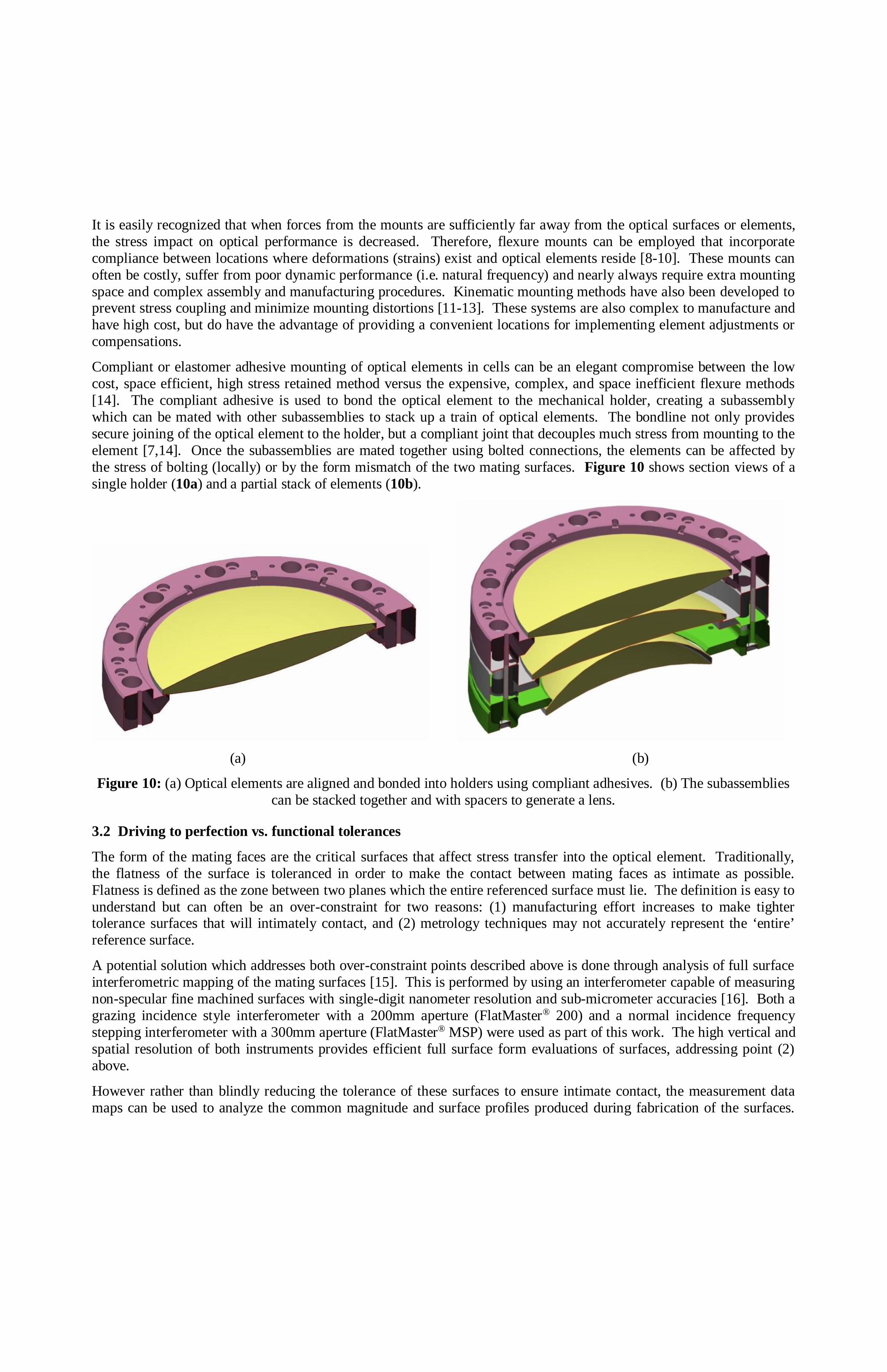
Compliant or elastomer adhesive mounting of optical elements in cells can be an elegant compromise between the low cost, space efficient, high stress retained method versus the expensive, complex, and space inefficient flexure methods [14]. The compliant adhesive is used to bond the optical element to the mechanical holder, creating a subassembly which can be mated with other subassemblies to stack up a train of optical elements. The bondline not only provides secure joining of the optical element to the holder, but a compliant joint that decouples much stress from mounting to the element [7,14]. Once the subassemblies are mated together using bolted connections, the elements can be affected by the stress of bolting (locally) or by the form mismatch of the two mating surfaces. Figure 10 shows section views of a single holder (10a) and a partial stack of elements (10b).
(a) (b)
Figure 10: (a) Optical elements are aligned and bonded into holders using compliant adhesives. (b) The subassemblies can be stacked together and with spacers to generate a lens.
3.2 Driving to perfection vs. functional tolerances
The form of the mating faces are the critical surfaces that affect stress transfer into the optical element. Traditionally, the flatness of the surface is toleranced in order to make the contact between mating faces as intimate as possible. Flatness is defined as the zone between two planes which the entire referenced surface must lie. The definition is easy to understand but can often be an over-constraint for two reasons: (1) manufacturing effort increases to make tighter tolerance surfaces that will intimately contact, and (2) metrology techniques may not accurately represent the ‘entire’ reference surface.
A potential solution which addresses both over-constraint points described above is done through analysis of full surface interferometric mapping of the mating surfaces [15]. This is performed by using an interferometer capable of measuring non-specular fine machined surfaces with single-digit nanometer resolution and sub-micrometer accuracies [16]. Both a grazing incidence style interferometer with a 200mm aperture (FlatMaster® 200) and a normal incidence frequency stepping interferometer with a 300mm aperture (FlatMaster® MSP) were used as part of this work. The high vertical and spatial resolution of both instruments provides efficient full surface form evaluations of surfaces, addressing point (2) above.
However rather than blindly reducing the tolerance of these surfaces to ensure intimate contact, the measurement data maps can be used to analyze the common magnitude and surface profiles produced during fabrication of the surfaces.

Analysis of the form deviations show mostly “low-order” variations in the circumferential or radial direction of the element holder faces; often coming from delicate machine alignments or clamping/fixturing of the parts during fabrication. Immediate improvement can be implemented when gross errors are recognized during this phase and can often be attributed to a machining or fixturing root cause. Recognition during this step alone can provide significant improvements to the manufacturing process.
Subtle errors and further quantification can be done with the use of appropriate filtering and decomposition of the measurement data. Fourier series fits or Fourier transforms are a useful tool that can be used to fit the mounting band surface measurements and separate specific orders of the low-order shape into individual “bins” or as shown in Figure 11.
(a)
(b) (c) (d)
Figure 11: (a) Interferometric flatness measurements of a holder face and are decomposed into low order form contributors such a (b) 2-lobe, (c) 3-lobe, and (d) radial taper using polynomial fitting.
Fourier filtering/decomposition
a.u.

Figure 11b and Figure 11c show the 2-lobe (astigmatic) and 3-lobe (trefoil) components of the flatness map from Figure 11a using a Fourier series fit in the circumferential direction of the flatness map. Figure 11d shows the extraction result of the flatness deviations with a radially oriented polynomial fit showing features such as radial taper or curvature similar to concavity or convexity of the mounting face. It is these low order shapes and shape mismatch between surfaces that most affect the bending stress when holders are mated to one another.
It is also important to note the overall flatness may contain excursions that are either sporadic or at spatial frequencies that will not affect the bending when two surfaces are bolted together. This impact is filtered out using the method described above allowing the important form features to be toleranced to a preferable level. Often this means that the GD&T interpretation can be loosened because of the analysis done with this type of metrology.
3.3 Results
The measurements of mating faces result in flatness maps of two subassemblies. In order to minimize cell bending during bolting in the assembly process, it is preferential to have low order form of the mating faces be of similar magnitude and the orientation, or phase, be complimentary. This is shown schematically below in Figure 12 for the 2-lobe (astigmatic) fit of the face flatness.
(a) (b)
Figure 12: (a) The 2-lobe form of the mating faces A and B are in phase (highs & lows align) which during bolting will maximize strain and (b) the 2-lobe form of the mating faces A and B are out of phase (high to low alignment) which will
be complimentary during bolting and minimize strain.
Because Fourier series fits of the mating surfaces are used, the coefficients of the nth order terms can be used to capture the magnitude and phase of the low order shapes. For example the 2-lobe forms shown in Figure 12 can be described using the function Ansin(n ) + Bncos(n ) where n=2. These are measured relative to a datum location on the circumference of the cell which can then be used to prescribe a rotation of one subassembly to the other to achieve a complementary phase.
2-lobe error sub-assy A
2-lobe error sub-assy B
2-lobe error sub-assy A
2-lobe error sub-assy B

4. CONCLUSION/SUMMARY The examples presented in this paper highlight the use of full surface characterizations that enable functional tolerancing of components which allows a loosening of the traditional flatness tolerance and provides a reduction in the cost and effort to manufacture. For EUV reticles, the techniques described provide a methodology for meeting image placement error requirements without shrinking flatness tolerances to levels that approach extreme to impossible. For DUV imaging objective lens holders, the full surface measurements provide data that can allow engineers to tolerance the appropriate low order shapes that most affect the stress into optical elements, often allowing the overall flatness of mating surfaces to become looser.
ACKNOWLEDGEMENTS
The authors would like to thank Michael Litzenberger and Todd McMichael of Corning Tropel Corporation for numerous contributions supporting the work within this paper.
REFERENCES
[1] Katherine Ballman, Chris Lee, Tom Dunn, Alexander Bean, "Error analysis of overlay compensation methodologies and proposed functional tolerances for EUV photomask flatness,” Proc. SPIE 9984, Photomask Japan 2016: XXIII Symposium on Photomask and Next-Generation Lithography Mask Technology, 99840S, (2016)
[2] Katherine Ballman, Christopher Lee, John Zimmerman, Thomas Dunn, Alexander Bean, "Evaluation of photomask flatness compensation for extreme ultraviolet lithography,” Proc. SPIE 9985, 99850N, Photomask Technology 2016, (2016)
[3] 2013 ITRS Lithography Roadmap, Table Lith6-EUV, www.itrs.net [4] Van Schoot, J, “EUV High-NA scanner and mask optimization for sub 8nm resolution,” Proc. SPIE 9635, 963503,
(2015) [5] Tsutomu Shoki, T. Yamada, S. Shimojima, Y. Shiota, M. Tsukahara, K. Koike, H.Shishido, O. Nozawa, T.
Sakamoto and M. Hosoya, “Development of EUV mask blanks with high flatness,” PMJ2008, April 17th, 2008. [6] Christina Turley, Jed Rankin, Xuemei Chen, Katherine Ballman, Christopher A. Lee, Tom Dunn, "EUV mask
flatness compensation strategies and requirements for reticle flatness, scanner optimization and E-beam writer (Conference Presentation),” Proc. SPIE 10450, 104500A International Conference on Extreme Ultraviolet Lithography 2017, (16 October 2017)
[7] Yoder, P.R., Jr., [Mounting Optics in Optical Instruments], SPIE Press, Washington, 127-178 (2008). [8] Bruning, J. H., DeWitt, F. A, Hanford, K. E., Decoupled mount for optical element and stacked annuli
assembly, US Patent 5428482. [9] Bacich, J.J., Precision lens mounting, European Patent 0230277B1. [10] Holderer, H., Rümmer, P., Trunz, M., Assembly of optical element and mount, US Patent 6229657B1. [11] Matsuyama, T., Shibazaki, Y., Ohmura, Y., Suzuki, T., “High NA and low residual aberration projection lens for
DUV scanner,” Proc. SPIE 4691, 687-695, (2002). [12] Dieker, T., Mounting Device for an Optical Element, US Patent 6552862B2. [13] Watson, D.C., Phillips, A. H., Hatasawa, M., Kinematic optical mounting assembly with flexures,
US Patent 6922293B2. [14] McMaster, B. M., Grejda, R. D., Dewa, P. G., “Advancements in the adhesive mounting of optics,” Proc. SPIE
10371, 1037103, (2017). [15] Grejda R. D., McMichael, T. R., Method of minimizing stacking element distortions in optical assemblies,
US Patent 9254538B2. [16] Corning Advanced Optics, “Optical Metrology,” http://www.corning.com/worldwide/en/products/advanced-
optics/product-materials/analytic-instruments.html (April 2018).