fine-grained and coarse-grained behavioral partitioning with effective utilization of memory and...
TRANSCRIPT
140 IEEE TRANSACTIONS ON VERY LARGE SCALE INTEGRATION (VLSI) SYSTEMS, VOL. 9, NO. 1, FEBRUARY 2001
Fine-Grained and Coarse-Grained BehavioralPartitioning with Effective Utilization ofMemory and Design Space Exploration
for Multi-FPGA ArchitecturesVinoo Srinivasan, Sriram Govindarajan, and Ranga Vemuri, Senior Member, IEEE
Abstract—Reconfigurable computers (RCs) host multiple fieldprogrammable gate arrays (FPGAs) and one or more physicalmemories that communicate through an interconnection fabric.State-of-the-art RCs provide abundant hardware and storageresources, but have tight constraints on FPGA pin-out andinter-FPGA interconnection resources. These stringent con-straints are the primary impediment for multi-FPGA partitioningtools to generate high-quality designs. In this paper, we presenttwo integrated partitioning and synthesis approaches for RCs. Thefirst approach involves fine-grained partitioning of a scheduleddata-flow graph (DFG, or an operation graph), and the secondinvolves a coarse-grained partitioning of an unscheduled controldata flow graph (CDFG, or a block graph). A hardware designspace exploration engine is integrated with the block graph par-titioner that dynamically contemplates multiple schedules duringpartitioning. The novel feature in the partitioning approaches isthat the physical memory in the RC is effectively used to alleviatethe FPGA pin-out and inter-FPGA interconnection bottle-neck.Several experiments have been conducted, targeting commercialmulti-FPGA boards, to compare the two partitioning approaches,and detailed summaries are presented.
Index Terms—Design space exploration, field programmablegate array (FPGA), partitioning, reconfigurable computers,synthesis.
I. INTRODUCTION
DESIGN process for reconfigurable computers (RCs) in-volves partitioning and synthesis of the given design spec-
ification onto the ield programmable gate arrays (FPGAs), andmemories on the RC and accordingly establishing the requiredpin-assignment and inter-FPGA routing. Partitioning of a designmay be performed at various levels, behavioral, register transferlevel (RTL) or gate-level. High level synthesis (HLS) processconverts a behavioral specification into a RTL design havingdata path (structural net list of components) and a controller. Be-havioral partitioning is a presynthesis partitioning, while struc-
Manuscript received February 17, 2000; revised August 25, 2000. This workwas performed at the University of Cincinnati, OH, and was supported in part bythe U. S. Airforce Research Laboratory, WPAFB, Dayton, OH, under ContractF33615–97–C-1043.
V. Srinivasan is with Intel Corporation, Santa Clara, CA 95054 USA (e-mail:[email protected]).
S. Govindarajan is with Cadence Design Systems, San Jose, CA 95134 USA(e-mail: [email protected]).
R. Vemuri is with the Department of ECECS, University of Cincinnati,Cincinnati, OH 45221 USA (e-mail: [email protected]).
Publisher Item Identifier S 1063-8210(01)01498-6.
tural partitioning is done after HLS. Studies such as [6]–[9]comparing behavioral and RTL partitioning show the superi-ority of the former for large designs.
Gate-level and RTL partitioning are both structural level par-titioning problems that are typically modeled as graph parti-tioning. In RTL partitioning, the nodes are components fromRTL library, while in gate-level partitioning the components arefrom the target specific device library. In fact, the same struc-tural partitioning engine has been used to perform both RTL andgate-level partitioning [10]. Problem sizes for gate level parti-tioning are a magnitude larger than for RTL partitioning. If theRTL components are preplaced macros [11], [12] that must notbe flattened into gates, then gate level partitioning is not per-formed. Usually gate-level partitioning is used in the contextof certain placement algorithms that use recursive partitioningstrategies to minimize the wire length [13].
Behavioral partitioners must be guided by high-level es-timators that make estimates on device area, memory size,input–output (I/0), performance and power. These estimationsare performed bylight weight synthesis estimators. Theseestimators have to be light weight because several thousandpartition options may be examined. However, being lightand accurate at the same time is very difficult. Sophisticatedestimation techniques are used to alleviate this difficulty [11],[12], [14]. Behaviorally partitioned system may use more gates,since hardware is not shared between partitions. However,since RTL partitions are I/O dominated, the RTL partitions donot tend to under utilize the device. Thus, this increase in gatesis not much of a concern.
The RC research community has invested several effortsinto multi-FPGA partitioning [15]–[22]. However almost all ofthese have been postHLS partitioning approaches. Chan et al.[15] partition with the aim of producing routable subcircuitsusing a prepartition routability prediction mechanism. Sawkarand Thomas [22] present a set cover based approach forminimizing the delay of the partitioned design. Limited logicduplication is used to minimize the number of chip-crossings oneach circuit path. Bi-partition orderings are studied by Hauckand Borriello [16] to minimize critical bottlenecks duringinter-FPGA routing. Woo [19], Kuznar [20], and Haung [21]primarily limit their partitioners to handle device area and pinconstraints. A library of FPGAs is available and the objectiveis to minimize device cost and interconnect complexity [20],
1063–8210/01$10.00 © 2001 IEEE
SRINIVASAN et al.: FINE-GRAINED AND COARSE-GRAINED BEHAVIORAL PARTITIONING 141
[21]. Functional replication techniques have been used [20]to minimize the cut size. Neogi and Sechen [17] presents arectilinear partitioning algorithm to handle timing constraintsfor a specific multi-FPGA system. Fang and Wu [18] present ahierarchical partitioning approach, integrated with RTL/logicsynthesis.
Behavioral partitioning has been promoted by several systemlevel synthesis groups [7], [14], [23]–[27]. In this paper, the be-havioral partitioning approach was chosen for RCs due to thedrawbacks of structural, as mentioned above, and due to sev-eral studies that lead to the decision [6], [7], [28], [29]. Wepresent two integrated partitioning and synthesis methodologiesRCs. In both approaches, we show that the physical memoryon the RC can be effectively used to alleviate the pin-out andinter-FPGA interconnection bottleneck. First, we present a dataflow graph (DFG) partitioner. Following this a coarser block-level partitioner is presented. The block-level partitioner is in-tegrated with a dynamic design space exploration engine. Thispaper presents a fully automated framework for behavioral par-titioning of a DFG and a control data flow graph (CDFG), withappropriate estimation and exploration techniques such that theRC resources are effectively utilized. In additional, the paperalso provides a detailed summary of advantages and disadvan-tages of both partitioning approaches.
Various aspects of the partitioning problem presented in thepaper and the hardware area/performance estimation techniquesbear similarities to the research in the area of hardware-soft-ware codesign [30]–[33]. There have been several approachesto solve the problem of hardware-software partitioning for arange of granularity [23], [31], [34]–[38]. Fully automatic par-titioners are in existence for quite some time now [23], [31],[35]. Gupta and De Micheli [23] start with an all hardware so-lution and iteratively move one task at a time to software untilno further improvement is possible. Ernst and Henkel [31] onthe contrary follow a software oriented approach which startswith an all software solution and uses a simulated annealingpartitioning engine. Hou and Wolf [35] proposed a process levelpartitioning heuristic based on hierarchical clustering. Eles [37]performs a performance guided partitioning based on simulatedannealing and Tabu search. Thomas [36] presents a coarse grainpartitioning methodology at a functional level. The RC parti-tioning presented in this work does not have a software estima-tion component. However, the communication model and the re-source availability (both for communication between partitionsand hardware logic) is well defined and performance overheadscan be accurately computed within clock-cycle accuracy. Thechallenge is to dynamically explore the hardware design spaceand efficiently use the available communication resources in-order to generate the optimal design that satisfies resource con-straints. It is typical of RC environment to have a host desk-topcomputer interacting with a FPGA-based RC. In such cases, RChardware partitioning can follow functional level hardware-soft-ware partitioning.
The SPARCS environment [12], [26], [62] developed atthe University of Cincinnati is a classic example of a tightlyintegrated system in that it has various partitioning, synthesis,and design space exploration engines that are coupled together.SPARCS provides a fully authomatic flow that converts a
high-level design specification into its temporally and spa-tially partitioned implementation on a generic reconfigurablecomputer. The work presented in this paper is an integral partof the SPARCS project and primarily focuses on the spatialpartitioning and design space exploration aspects in SPARCS.
This paper is organized as follows. In Section II, the DFGand block graph specification models are presented. Section IIIpresents the target RC architecture model. Sections IV and Vpresent in detail the data flow graph and block graph parti-tioning methodologies, experimental results, and observations.Our conclusions are presented in Section VI.
II. I NPUT SPECIFICATION MODELS
In this section, we formally present the two specificationmodels that are used this paper—data flow graph, and behav-ioral block graph.
A. Specification for Fine-Grained Partitioning
Several digital signal processing (DSP) and image processingapplications can be expressed as simple graphs that have puredata flow or minimal control flow. Discrete cosine transforms(DCT), fast Fourier transforms (FFTs), image filtering, and Ja-cobi transforms are some widely used applications that can beexpressed by data flow graphs.
The input to be partitioned is an acyclic graph whose nodesare the operations to be partitioned across the FPGAs of the RCand the edges represent the data flow. The formal definition isas follows.
Definition II.1: A DFG is a directedacyclic graph,. is the set of nodes representing the operations
and is the set of directed hyper-edges corresponding to thedata flow dependencies.is the set of primary inputs and isthe set of primary outputs. Following are the attributes relatedto nodes and edges.
• For each node : is the area of the nodesin configurable logic blocks (CLBs); is the number ofinput wires feeding ; is the number of output wiresfanning out ; and is the level number of the node, or its schedule time-step. For a valid DFG
Here, the symbol denotes a directed path.• For each edge : is the source node or the
primary input, in , that drives the hyper-edge; isthe set of nodes and primary outputs that are driven bythe hyper-edge . , is the bit width of the edge,and is the data-transfer mode for the edge, if itcutspartition boundaries. If MEM, then datatransfer is through memory transfer, else WIREand data-transfer is through the interconnection networkof the RC.
is a scheduled data flow graph with well defined modes fordata transfer across partitions. All primary inputs to the DFGmustbe available when the DFG starts execution (at time-stepzero). Primary outputs are available in the next time-step afterthey are computed.
142 IEEE TRANSACTIONS ON VERY LARGE SCALE INTEGRATION (VLSI) SYSTEMS, VOL. 9, NO. 1, FEBRUARY 2001
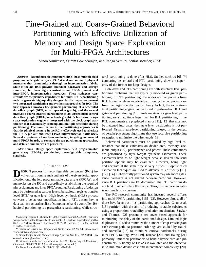
Fig. 1. Vprod: DFG for8� 8 vector product.
Fig. 1 shows the DFG for a vector product equation ofthe form . The DFG is sched-uled in five time-steps. The level of an operation is the time step(level) at which it is scheduled. For instance, in Fig. 1, four op-erations have the level attribute value of zero. All primary inputsto the DFG are fetched from the memory and all primary out-puts must be stored in memory. All internal nets by default areMEM mode unless explicitly specified asWIRE. In Fig. 1, twoedges haveWIREmode, meaning, if these nets are cut duringpartitioning, then they must be wired using the interconnect re-sources on the board.
B. Specification for Coarse-Grained Partitioning
Thebehavioral block graphin essence is a CDFG where theblocks in the graph capture the data flow in the design and theedges across blocks capture both control flow and data transfers.The block graph is extracted from the behavioral specification ofthe design and is used as the intermediate format for the AssertaHLS [39], [40]. Here is a more formal definition of the BBG.
Definition II.2: A BBG is a directed graph,PI PO , where
is the set of behavioral blocks in thedesign.PI and PO are the primary input and primary outputports of the design.
CE CE CE is the set of control dependen-cies in the BBG. Each control edge,CE ,denotes control dependency from BB to the set of BBs in
. The control transfer from block to one of the blocksin happens conditionally based on the value thatsetson the flag . Informally, each control edge is a multi terminaledge from a source block to multiple destination blocks, wherethe control transfer from source to one of the destination blocksoccurs conditionally. Data transfer takes place from the outputport of a block to the input port of another.
DE DE DE is the set of data dependenciesin the BBG. Each data transfer edge,DE
, denotes multiterminal net with BB as the source and theset of BBs in are the destination. denotes the width ofthe data transfer edge. The source of the data transfer may be aprimary input port inPI and similarly one or more destinations
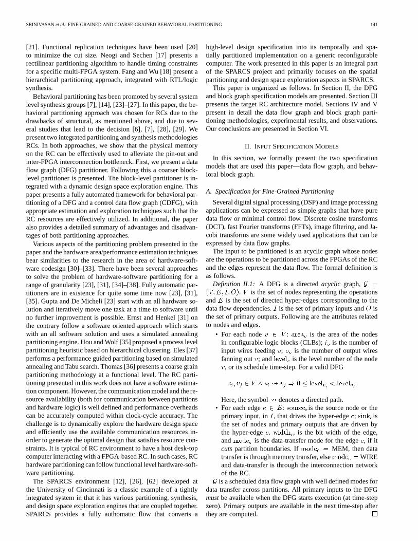
(a)
(b)
Fig. 2. Examples of a block graph, extracted from BBIF.
may be primary output ports inPO. The variable denotesthe data-transfer mode (Definition II.1) ofDE .
Each BB is modeled as a quadruplewhere is the DFG that represents the
behavior of the block . follows the DFG semantics,Definition II.1. and are the input and output ports ofthe behavior block . The input ports of the block may beconnected to one of the primary inputs (PI) or to the outputports of other blocks. Similarly ports in may be connectedto primary outputs (PO) and/or to inputs ports of other blocks.The port connectivity is also captured by the data dependencyset, .
Fig. 2(a) shows a block graph with six behavioral blocks.Fig. 2(b) shows the structure of a single block. Block B1 per-forms operations on the primary input and the control is trans-

SRINIVASAN et al.: FINE-GRAINED AND COARSE-GRAINED BEHAVIORAL PARTITIONING 143
Fig. 3. Block graph of 2-D FFT.
Fig. 4. The reconfigurable architecture model.
fered to B2. On completion of B2, the controlconditionallytransfers to block B3 or B4. B5 executes next when either ofB3 or B4 finishes and finally B6 is executed.The block graphmodel permits only a single thread of control. Exactly one blockis active at any time during the execution of the design. This al-lows acomplete sharing of resources across blocks. The blockgraph model allows operation-level parallelism within the be-havioral blocks. Control constructs such asif then else, caseandwhile loopsin BBIF can easily be translated into control flow inthe block graph [39], [40]. Fig. 3 shows the BBG for the two-di-mensional (2-D) FFT benchmark. The graph has 18 blocks and25 edges. Notice that there are two loops in the graph.
III. T ARGET RC MODEL
We consider a multi-FPGA RC architecture that has multipleFPGAs sharing a single physical memory. The FPGAs are inter-connected by a fixed interconnection network and all the FPGAscan access the memory through a shared memory bus. Fig. 4shows the RC architecture model that is considered.
Formally, the RC has FPGAs, thatshare a physical memory . For , is the area ofthe FPGA in terms of the available CLBs. We define conn tobe the connectivity matrix, where for conn
is the number of wires in the channel connecting FPGA-and
FPGA- . The connectivity matrix is derived from the the fixedinterconnection network.
The FPGAs can communicate data either through the sharedmemory or directly throughchannels(wires) in the intercon-nection network. For DFG and block graph partitioning, all pri-mary design inputs are assumed to be present in the memory andall primary outputs are written back to the memory. For DFGpartitioning, when the internal edges in the DFG are cut, datacommunication is made through either memory or channels de-pending on their user-specified mode (Definition II.1).
IV. DATA FLOW GRAPH PARTITIONING
In this section, we present the DFG partitioning methodology.First, we explain the partitioning and synthesis process. Fol-lowing this the various details about the cost estimation and par-tition evaluation methodologies are presented. We briefly de-scribe the iterative partitioning engine used. Elaborate experi-mental results are presented and the observations are summa-rized at the end of this section.
A. Partitioning and Synthesis Process for DFGs
The goal of RC synthesis process is to partition and synthe-size a behavioral specification and toefficiently utilizethe un-derlying RC resources. The quality of the design is determinedby the cost metrics, discussed later in Section IV-B. The primarygoal of this process is to successfully obtain a partitioned designthat satisfies all board-level constraints such as area, intercon-nect, and memory resources. The secondary, but an importantfactor is measured in terms of the performance (throughput) ofthe design.
Fig. 5 shows the partitioning and synthesis design flow forDFG partitioning onto RCs. First the DFG is extracted froma behavioral specification in C [41] or very high speed inte-grated circuit hardware description language (VHDL) [42]. De-sign space exploration is performed to generate aschedule[43]for the DFG that is suitable for the underlying RC. The sched-uled DFG is then passed as an input to the partitioner. The DFGpartitioner generates multiple CDFGs. Each CDFG is synthe-sized for an individual FPGA on the RC. Thecontrolstructuresin the CDFG are a simple synchronization mechanism betweenthe multiple communicating DFGs.
Any iterative partitioning engine such as simulated annealing(SA) [44], genetic algorithm (GA) [45], or Fiduccia–Mattheyses(FM) may be used by the partitioner. The most crucial com-ponent of the partitioner that determines its convergence is thepartition cost evaluator. The evaluator estimates the cost andperformance of the contemplated partition against the target RCmodel, as presented in Section IV-B.
Following partitioning, we generate a block graph (CDFG)for each partition segment of the original DFG. Each blockgraph is then individually synthesized to a RTL implementa-tion by the Asserta [39] HLS tool. Asserta is a formally assertedhigh-level synthesis system, that can produce RTL designs forany user specified RTL component library. The RTL designsproduced by Asserta have two components. The first compo-nent is a simple finite state machine (FSM) that acts as the con-troller and the second component is data path of components

144 IEEE TRANSACTIONS ON VERY LARGE SCALE INTEGRATION (VLSI) SYSTEMS, VOL. 9, NO. 1, FEBRUARY 2001
Fig. 5. RC partitioning and synthesis process for DFGs.
from the RTL component library. The synthesized designs aretranslated to VHDL, integrated together with the RC VHDLtemplates, usually provided by the RC vendor. The integrationprocess involves connecting the design I/O to the pads in theRC template and generating additional glue logic, if necessary.Commercial VHDL simulators are used to simulate the parti-tioned design and verify timing and functionality of the parti-tioned design.
After successful RTL simulation, logic and layout synthesis isperformed on each design that is mapped to an FPGA. The tem-plate host program is accordingly modified to setup the memoryfor inputs and provide the necessary signals to start and recog-nize the finish of the design on the RC. Finally, the design isdownloadedon the RC and board-level testing is performed. Inpractice, layout synthesis may fail during place and route. Theinformation is fed back to the partitioner, respective constraintsare tightened and the design process is carried out again. Due tothis time-expensive design cycle, the cost evaluators are care-fully finetuned so that such failures, late in the design process,can be minimized.
B. Partition Cost Evaluation for DFG Partitioning
Partitions are evaluated based on their architectural con-straint-satisfaction and how well the performance is optimized.For DFG partitioning we consider number and area of theFPGAs and the inter-FPGA interconnection resources to be theconstraints on the RC. The RC constraints are available fromthe RC architecture model (Fig. 5). The optimization goal forthe partitioner is to minimize the latency of the design. Beforepresenting the combined cost function, the area, interconnectand latency estimation techniques are presented.
1) Area Estimation:The area of each partition segmentis constrained by the number of CLBs available on the FPGAto which it is mapped. In the case of ASIC design, both com-putation resources (ALU components such as, adders and sub-tracters) and storage resources (registers) are considered alikebecause both occupy silicon area. However, in FPGAs, the loopup table (LUT) based function generators in the CLBs providethe computation resources while the flip-flops in the CLBs pro-vide the storage resources. Hence, in the case of FPGAs, com-putation area estimation and storage area estimation (registerestimation) must be performed separately and individual con-straint-satisfaction checked.
The total area of a segment is composed of the componentarea, multiplexor areas due to component and register sharing.The area of each component is available from the RTL library.Multiplexor area characterization for Xilinx 4000 series FPGAs[49] shows that a four-input multiplexor needs a unit CLB re-source and the area increases linearly with the input size.
During synthesis, all inputs and outputs of every node in theDFG is stored in a register. Trivially if every input and outputbit of a node is stored in a flip-flop, then the storage resource re-quired is a function of sum of the I/O bits of all nodes in the par-tition segment. Approximately, for every two 4-bit registers thatare shared, a unit CLB cost will be incurred for multiplexing. Weuse empirical formulas to compute the register and multiplexorarea costs [46] based on an expected register sharing behavior.
Let be the segments to be mapped onto theFPGAs on the RC (Section III). Then, we define theAreaPenaltyof the partition as
AreaPenalty
where
otherwise
is the estimated area of the segmentand(Section III) is the area of the FPGA to which the segment ismapped. Notice that no negative penalties are assigned to seg-ments with areas lesser than the FPGA area. More importantlywe normalize the area violations to the amount of area avail-able. This is important when partitions are evaluated for mul-tiple conflicting constraints. A value of zero for theAreaPenaltyimplies that the partition does not violate area constraint. Neg-ative area penalties are avoided because the goal is to generatethe performance-optimal design that does not violate resource

SRINIVASAN et al.: FINE-GRAINED AND COARSE-GRAINED BEHAVIORAL PARTITIONING 145
constraints for a fixed RC. Negative penalties needlessly avoidsearch spaces thereby increasing the chances of beign held at alocally optimal solution.
2) Interconnect Estimation:The inter-FPGA interconnec-tion resource constraints are derived from the connectivitymatrix (conn) that is part of the RC specification model(Section III). Let be the partition segments.Each edge in the original DFG contributes a wire requirementof size , if is Wire and edge communicatesbetween two different segmentsand . Another componentthat adds to the interconnection cost is the routing of synchro-nization lines for the communicate the end of a block execution.
Let be the segments to be mapped onto theFPGAs on the RC (Section III). For
be the number of wires required between partition segmentsand (as computed by the functionEstimate Wires .Then, we define theInterconectPenaltyof the partition as
InterconnectPenalty where
ifotherwise
Notice that similar to theAreaPenaltycomputation (Sec-tion IV-B.1), no negative penalty is assigned for constraintsatisfying solutions. Again, the interconnect penalty is normal-ized with respect to the number of channels available on theRC for inter-FPGA routing.
3) Latency Estimation and Memory Utilization:A partitionsolution of a DFG is constraint-satisfying if both area and in-terconnect penalties are zero. When multiple constraint satis-fying partitions are obtained, the partitioner selects the solutionwith the least design latency. Latency is the the total number of-steps (clocks) to process a single set of inputs to the DFG. If
the input specification were not partitioned but implemented ona single FPGA the total latency will be the schedule length of theDFG plus the time for reading primary inputs from the memoryand writing primary outputs back to the memory.
In the case of a partitioned DFG, additional clocks are spentin data transfer across partitions and in synchronization of blockexecution across multiple segments. The latency of a partitioneddesign is composed of four components.
1) DFG schedule length: This is the number of time steps inthe scheduled DFG. This is equal to the maximum of thelevel numbers of all nodes in the DFG. Formally, schedulelength , refer Definition II.1.
2) I/O latency: Primary inputs and outputs are stored in thememory. Since we consider a shared memory RC model,the I/O latency is a linear function of the number of pri-mary inputs and outputs of the DFG. If each memory readand write operation takesand cycles, then the I/O la-tency for a DFG is(Definition II.1). For the Wildforce [1] architecture, is3 cycles and is one cycle.
3) Data transfer latency: When edges in the DFG cut seg-ment boundaries, the data transfer between FPGAs maybe either through the shared memory or through the chan-nels in the interconnection network. Each data transfer
through memory will consume cycles, and eachwired data transfer will consume two cycles, assumingunit cycle for port read and write. If there are datatransfers through memory and wired data transfersthen the data transfer latency is .
4) Synchronization latency: Insertion of synchronizationblocks introduces extra clock ticks to write the donesignal and recognize it. The synchronization latency is thenumber of synchronization blocks in the design multipliedby a constant factor. The value of the constant dependson the synthesis process. The HLS tool used (Asserta[39]) in our partitioning environment (Fig. 5) consumesfour extra cycles for every synchronization block.
The total latency is the sum of the four components discussedabove. As seen from the above discussion, the latency of thethe design can be accurately computed and the time to computelinearly increases with the number of edges in the DFG.
C. Partitioning Engine for DFG Partitioning
We use a GA [45], [50] based partition engine to performthe DFG partitioning. GAs capture the solution in a structuralrepresentation and the convergence is based on genetic oper-ations—selection, crossover and mutation. The genetic opera-tors work on a population of solutions, also called generation.We now present the details of the adaptation of GA for DFGpartitioning. We model the partitioning problem as a simple in-teger-coded genetic algorithm. Each partition solution is repre-sented as an integer array whose length is equal to the number ofnodes in the DFG and the each location of the array has a valuebetween one and the number of partition segments. The selec-tion operator probabilistically selects highly fit solutions in thecurrent generation. The GA uses uniform crossover operation[51]. Mutation operator randomly changes the integer values inthe integer arrays. The population size varies between 100 and200. Selection percentage is set to20%, and mutation proba-bility is 0.10.
The convergence of the GA is primarily dependent on thefitness computation function.
fitness
AreaPenalty InterconnectPenalty(1)
Equation (1) shows how fitness of a partitionis computed.AreaPenaltyandInterconnectPenaltyare computed as presentedin Sections IV-B.1 and IV-B.2. Thus, when both area and inter-connect penalties are zero, the fitness of the solution is one.
The selection operator firstsortsthe solutions in the currentpopulation in decreasing order ofquality[(2)]. For two solutions
and , the solution with
quality quality
(2)
where and are the fitness and latency values for the so-lution .
The selection operator selects20%of the population, with ahigh probability of selecting solutions lower (high quality solu-tions) in the sorted array. Selecting the lower20%of the sorted
146 IEEE TRANSACTIONS ON VERY LARGE SCALE INTEGRATION (VLSI) SYSTEMS, VOL. 9, NO. 1, FEBRUARY 2001
array may make the GA converge too fast. The crossover oper-ator also selects good quality solutions for crossover.
D. Experimental Results for DFG Partitioning
In this section, we present the results of partitioning severalDFG benchmarks of varying sizes onto multi-FPGA RC archi-tectures. The genetic partitioning engine and the estimation al-gorithms are implemented in C++ and all results are reportedfor a two processor Sun UltraSparc workstation running at 296Mhz and 384 MB RAM.
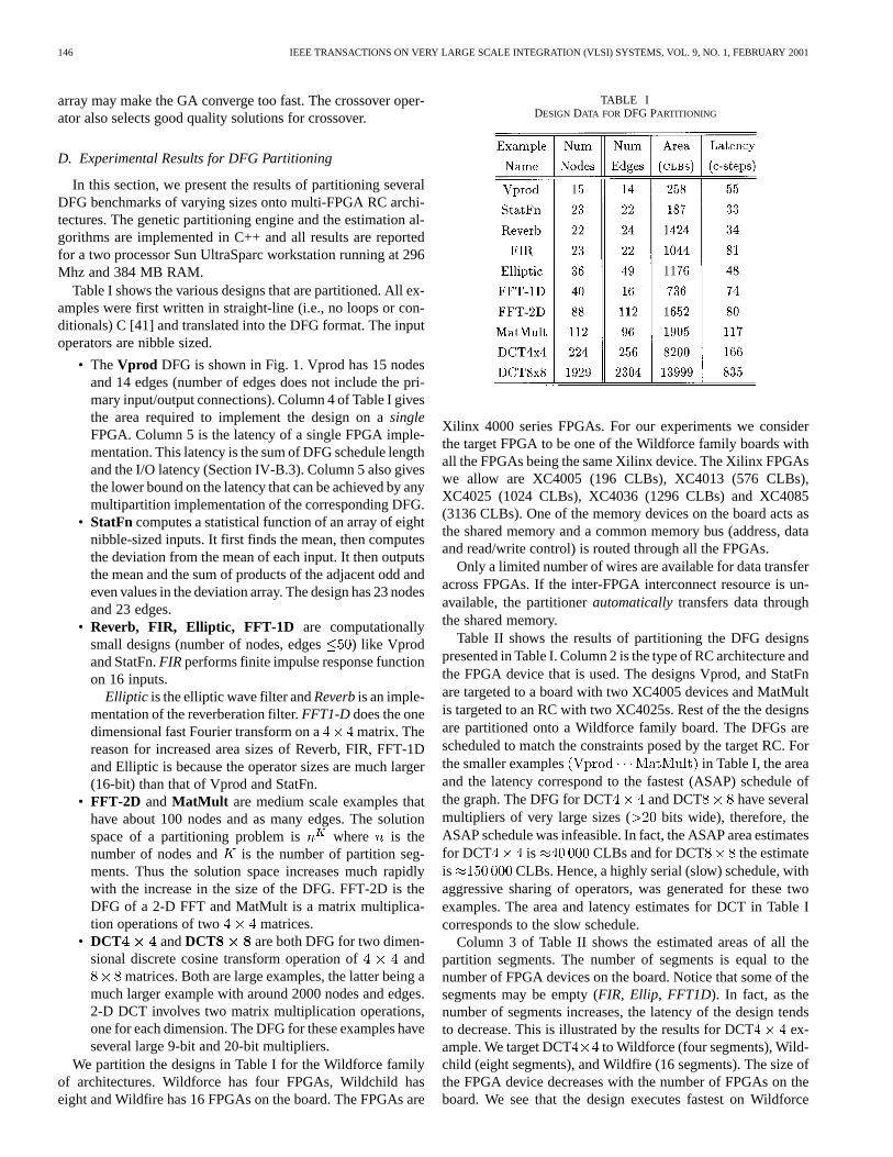
Table I shows the various designs that are partitioned. All ex-amples were first written in straight-line (i.e., no loops or con-ditionals) C [41] and translated into the DFG format. The inputoperators are nibble sized.
• TheVprod DFG is shown in Fig. 1. Vprod has 15 nodesand 14 edges (number of edges does not include the pri-mary input/output connections). Column 4 of Table I givesthe area required to implement the design on asingleFPGA. Column 5 is the latency of a single FPGA imple-mentation. This latency is the sum of DFG schedule lengthand the I/O latency (Section IV-B.3). Column 5 also givesthe lower bound on the latency that can be achieved by anymultipartition implementation of the corresponding DFG.
• StatFn computes a statistical function of an array of eightnibble-sized inputs. It first finds the mean, then computesthe deviation from the mean of each input. It then outputsthe mean and the sum of products of the adjacent odd andeven values in the deviation array. The design has 23 nodesand 23 edges.
• Reverb, FIR, Elliptic, FFT-1D are computationallysmall designs (number of nodes, edges ) like Vprodand StatFn.FIR performs finite impulse response functionon 16 inputs.
Elliptic is the elliptic wave filter andReverbis an imple-mentation of the reverberation filter.FFT1-Ddoes the onedimensional fast Fourier transform on a matrix. Thereason for increased area sizes of Reverb, FIR, FFT-1Dand Elliptic is because the operator sizes are much larger(16-bit) than that of Vprod and StatFn.
• FFT-2D andMatMult are medium scale examples thathave about 100 nodes and as many edges. The solutionspace of a partitioning problem is where is thenumber of nodes and is the number of partition seg-ments. Thus the solution space increases much rapidlywith the increase in the size of the DFG. FFT-2D is theDFG of a 2-D FFT and MatMult is a matrix multiplica-tion operations of two matrices.
• DCT andDCT are both DFG for two dimen-sional discrete cosine transform operation of and
matrices. Both are large examples, the latter being amuch larger example with around 2000 nodes and edges.2-D DCT involves two matrix multiplication operations,one for each dimension. The DFG for these examples haveseveral large 9-bit and 20-bit multipliers.
We partition the designs in Table I for the Wildforce familyof architectures. Wildforce has four FPGAs, Wildchild haseight and Wildfire has 16 FPGAs on the board. The FPGAs are
TABLE IDESIGN DATA FOR DFG PARTITIONING
Xilinx 4000 series FPGAs. For our experiments we considerthe target FPGA to be one of the Wildforce family boards withall the FPGAs being the same Xilinx device. The Xilinx FPGAswe allow are XC4005 (196 CLBs), XC4013 (576 CLBs),XC4025 (1024 CLBs), XC4036 (1296 CLBs) and XC4085(3136 CLBs). One of the memory devices on the board acts asthe shared memory and a common memory bus (address, dataand read/write control) is routed through all the FPGAs.
Only a limited number of wires are available for data transferacross FPGAs. If the inter-FPGA interconnect resource is un-available, the partitionerautomaticallytransfers data throughthe shared memory.
Table II shows the results of partitioning the DFG designspresented in Table I. Column 2 is the type of RC architecture andthe FPGA device that is used. The designs Vprod, and StatFnare targeted to a board with two XC4005 devices and MatMultis targeted to an RC with two XC4025s. Rest of the the designsare partitioned onto a Wildforce family board. The DFGs arescheduled to match the constraints posed by the target RC. Forthe smaller examples in Table I, the areaand the latency correspond to the fastest (ASAP) schedule ofthe graph. The DFG for DCT and DCT have severalmultipliers of very large sizes ( bits wide), therefore, theASAP schedule was infeasible. In fact, the ASAP area estimatesfor DCT is CLBs and for DCT the estimateis CLBs. Hence, a highly serial (slow) schedule, withaggressive sharing of operators, was generated for these twoexamples. The area and latency estimates for DCT in Table Icorresponds to the slow schedule.
Column 3 of Table II shows the estimated areas of all thepartition segments. The number of segments is equal to thenumber of FPGA devices on the board. Notice that some of thesegments may be empty (FIR, Ellip, FFT1D). In fact, as thenumber of segments increases, the latency of the design tendsto decrease. This is illustrated by the results for DCT ex-ample. We target DCT to Wildforce (four segments), Wild-child (eight segments), and Wildfire (16 segments). The size ofthe FPGA device decreases with the number of FPGAs on theboard. We see that the design executes fastest on Wildforce

SRINIVASAN et al.: FINE-GRAINED AND COARSE-GRAINED BEHAVIORAL PARTITIONING 147
TABLE IIRESULTS FORDFG PARTITIONING
architecture, followed by Wildchild then the Wildfire. The la-tency of an unpartitioned design (reported in Table I), providesa lower bound on the design latency. Column 5 of Table II re-ports the latency of the partitioned design. Notice that more thenumber of partition segments, greater is the deviation from thelower bound.
The estimated area of the unpartitioned DFG (as in Table I isthe lower bound on the total area. Column 4 of Table II reportsthe total area of the partitioned designs. We infer from the resultsthat limited larger FPGAs is a better alternative than severalsmaller FPGAs. The run times for the genetic algorithm rapidlyincreases with the size of the DFG. The last column in Table IIreports the execution time to complete 1000 generations of thegenetic algorithm.
For a few examples (Table III), we performed logic and layoutsynthesis and compared our estimated area and performancemeasures against the actual values after synthesis. The designsVprod and StatFn were successfully implemented and testedon the Wildforce [1] board. Table III shows estimated and ac-tual areas after synthesis of the partition segments for each de-sign. Similarly, the estimated and actual latency (obtained fromRC VHDL template simulation) of the partitioned design is re-ported. We observe a very small deviation in the latency com-putation. The deviation in area estimates and actual area is dueto the approximations made for interconnect and the controllerarea. However, the error margin is less than20%, making theestimation process reliable.
TABLE IIIRESULTS OFLAYOUT SYNTHESIS AND ON-BOARD TESTING
E. Observations and Summary for DFG Partitioning
We presented a simple and efficient methodology for parti-tioning data-flow graphs onto multi-FPGA shared memory RCarchitectures. A fully automatic design flow from a behavioralspecification in C or VHDL is accomplished. There are variousadvantages of this process.
• For small designs, it is straight forward to specify the de-sign as a DFG.
• The user is oblivious to the underlying RC architecture.The specification is implementation independent. The datatransfers and the DFG i/o are automatically mapped to thememory or the inter-FPGA wires automatically.

148 IEEE TRANSACTIONS ON VERY LARGE SCALE INTEGRATION (VLSI) SYSTEMS, VOL. 9, NO. 1, FEBRUARY 2001
• Given a scheduled DFG, area and latency of the parti-tioned design can be estimated with reasonable accuracy.
• The partitioned implementation exploits the inherent op-erator level parallelism in the DFG. Multiple operations inthe same and different FPGAs may be active at the sametime.
• Typically, pin-outs and inter-FPGA routing resources areone of the primary bottlenecks to implement large de-signs on RCs. Our DFG partitioning methodology is anapproach to minimize this bottleneck by seamlessly trans-ferring inter-FPGA communication through the memory.This is done at the cost of increased latency of the design.However,if not for this, most of the useful designs tend tobe infeasible.
• The partitioned design model is simple and closely resem-bles the original DFG in its structure. The simple parti-tioning process poses very limited scope for error whengenerating the partitioned design. Moreover verificationof the partitioned design is not difficult.
The advantages of DFG partitioning come with several dis-advantages as well.
• The design space exploration process is not fully inte-grated with the partitioning process. Since partitioning isdone at a fine-grained level (operation-level partitioning),the problem size increases exponentially with the numberof nodes. Design space exploration (i.e., determination ofan efficient schedule of operations), during partition is ex-tremely time consuming and is feasible only for very smallexamples. In the DFG partitioning methodology, designspace exploration is performeda priori based on the con-straints posed by the target RC.
• The lack of control structures, such as conditionalbranching and loops, makes it tedious to specify largerdesigns. For ease of specification, if control constructssuch as loops were allowed, the following are the draw-backs: 1) the transformation process into a DFG may becomplex and prone to errors; and 2) verification of thespecification against the final design will be much moredifficult.
The DFG model is insufficient to express designs withcontrol flow, a traffic light controller, for instance. How-ever, DFG specification is useful for a restricted domainof data dominant applications.
• Due to operator level partitioning, the problem size ismuch larger than functional partitioning. For instance, apartitioning Matrix multiplication DFG is severaltimes faster than an multiplication. This is not trueabout block level or function level partitioning. As seenfrom the results (Table II), run times for DCT designis several days.
We see a need for coarser grain partitioners that keep thepartition problem size within reasonable limits. Integrateddesign space exploration during partitioning is possible withcoarser grain partitioners but not during DFG partitioning.Control structures such as loop and conditionals enhance theapplicability of the methodology. RCs with fewer and largerFPGAs are more useful than those with several smaller devices.
Fig. 6. Synthesis and partitioning environment for block graphs.
V. BLOCK GRAPH PARTITIONING
In this section, we present the block graph (coarse-grained)partitioning methodology. We illustrate the advantages of inte-grated design space exploration during partitioning. The designspace exploration engine and the various cost estimation tech-niques are described in adequate detail.
A. Partitioning and Synthesis Process for BBGs
Fig. 6, shows our approach to integrated synthesis and parti-tioning. The design to be partitioned is specified in a high levelspecification language such as VHDL [42] or C [41]. The inputtranslator converts the specification into an equivalent blockgraph specification (Section II-B). A profiler computes the av-erage execution count (AEC) and maximum execution count(MEC) for each behavioral block in the (block graph). The AECof a block is the average number of times the block is invokedper profile vector, averaged over a large set of profiling stimuli.The MEC of a block is the maximum number of times the blockis invoked during any single profile run. AEC values of blocksmay be greater than one in the presence of loops and they maybe fractional values less than one due to conditional invocationof blocks.
The core of the environment is the HLS exploration engine[52] integrated with an iterative partitioning engine. The uniquefeature of the exploration engine is that it views a partitionedmodel of the block graph and performs design space explorationto globally optimize the partitioned design. Traditionally, de-sign space exploration engines [53]–[57] do not consider parti-tioned design models for exploration. Instead area-time tradeoffcan be performed on each partition without the knowledge ofother partitions. Thus each partition is locally optimized butglobal optimization of the partitioned design cannot be per-formed. We explain the multipartition exploration engine in

SRINIVASAN et al.: FINE-GRAINED AND COARSE-GRAINED BEHAVIORAL PARTITIONING 149
Fig. 7. Model for the exploration engine.
Section V-B, and a more detailed description and analysis maybe found in [52].
The partitioner has iterative partitioning engines such as theSA and the FM heuristics. The partitioners interact with theexploration engine through an application program interface(API). The API provides various useful functions that are usedto efficiently perform design space exploration on a partitionedblock graph. The various API functions and the modes ofinteraction between the partitioner and the exploration engineare presented in SectionsV-B and V-D.
The result of partitioning is a collection of block graphs, onefor each partition segment of the original block graph. Eachpartition segment is targeted to a single FPGA on the RC. HLSis performed on each partitioned block graph and a set of RTLdesigns are generated. Logic and layout synthesis is performedon the partitioned designs to generate the required configura-tion streams for the FPGAs. In our design process, the Assertasystem [39] is used to perform HLS. Commercial simulation(Synopsys’ VHDL simulator), logic synthesis (Synplicity’sSynplify) and layout synthesis (Xilinx M1) tools are used.
B. Design Space Exploration Engine
The exploration engine [52] provides the framework to inte-grate any iterative partitioner, such as SA, FM, and GA. The par-titioners can invoke the exploration algorithm through a rangeof interface functions and get area and latency estimates aboutindividual blocks, partition segments, or for the complete parti-tioned design itself. In addition to estimation, the explorationengine can efficiently explore the design space of the blocks(finding the best schedule for each partition segment), such thata constraint-satisfying solution that is optimal in terms of la-tency is produced.
Fig. 7 shows the exploration model. On the left is the parti-tioned block graph. Each segment,, has a set of design pointsassociated with it, . The design points areshown in the center of the Fig. 7. Each design point corre-sponds to a particular schedule of the segment. A schedule ofthe segment , is derived from the schedule of the individualblocks in and the sharing information between the blocks.Given a design point for a segment, various estimates about
Fig. 8. Block diagram of the HLS exploration engine.
the RTL design corresponding to that design point can be made.These estimates include details about ALU, register, and multi-plexor areas. In addition, the controller information such as thenumber of states, inputs and outputs are also available. The ex-ploration engine also maintains the necessary information aboutsharing of resources within and across the blocks in any seg-ment.
The overview of the exploration engine is presented in Fig. 8.The inputs to the exploration are the BBIF corresponding totheblock graphto be partitioned (withblocks assigned to seg-ments), thedesign latency constraint, and the characterized RTLcomponent library. The exploration engine has three main com-ponents: 1) the design analyzer; 2) the design explorer; and 3)the application program interface (API) to the partitioner. Theexploration engine also has a resource estimator, fast time-con-strained and resource-constrained schedulers and a behavioralestimator that can estimate the area and performance of the RTLdesign corresponding to a scheduled block graph.
The first call made by the partitioner to the explorationengine is to initialize the exploration engine and setup partitioninvariant information about the design. Thedesign analyzermodule does such initialization. Following are the phases ofthe design analyzer:
1) initialization: dependency graphs for each block and theentire control flow graph of the design is built;
2) resource estimation: for each block in the graph alocalresource setis formed. The resource set contains compo-nents from theRTL library that are potentially required toimplement the block. Aglobal resource set for the entiregraph is formed based on the individual local sets;
3) design latency function: The function to compute the de-sign latency is determined. Design latency is the numberof clock cycles required for a single execution of the de-sign. The design latency, , is the sum of the number ofclocks spent in each block of the design. Formally
is the execution count of the block. The execu-tion count may either be set to the AEC or MEC of theblock. This choice is made by the user. Usually, the AECis the default choice unless the latency constraints are verycrucial andmustnot be violated. The user may choose to
150 IEEE TRANSACTIONS ON VERY LARGE SCALE INTEGRATION (VLSI) SYSTEMS, VOL. 9, NO. 1, FEBRUARY 2001
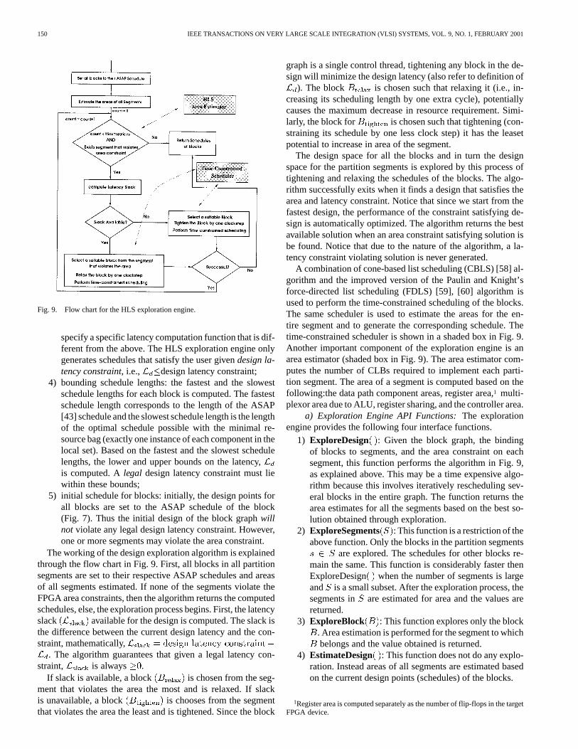
Fig. 9. Flow chart for the HLS exploration engine.
specify a specific latency computation function that is dif-ferent from the above. The HLS exploration engine onlygenerates schedules that satisfy the user givendesign la-tency constraint, i.e., design latency constraint;
4) bounding schedule lengths: the fastest and the slowestschedule lengths for each block is computed. The fastestschedule length corresponds to the length of the ASAP[43] schedule and the slowest schedule length is the lengthof the optimal schedule possible with the minimal re-source bag (exactly one instance of each component in thelocal set). Based on the fastest and the slowest schedulelengths, the lower and upper bounds on the latency,is computed. Alegal design latency constraint must liewithin these bounds;
5) initial schedule for blocks: initially, the design points forall blocks are set to the ASAP schedule of the block(Fig. 7). Thus the initial design of the block graphwillnot violate any legal design latency constraint. However,one or more segments may violate the area constraint.
The working of the design exploration algorithm is explainedthrough the flow chart in Fig. 9. First, all blocks in all partitionsegments are set to their respective ASAP schedules and areasof all segments estimated. If none of the segments violate theFPGA area constraints, then the algorithm returns the computedschedules, else, the exploration process begins. First, the latencyslack available for the design is computed. The slack isthe difference between the current design latency and the con-straint, mathematically,
. The algorithm guarantees that given a legal latency con-straint, is always .
If slack is available, a block is chosen from the seg-ment that violates the area the most and is relaxed. If slackis unavailable, a block is chooses from the segmentthat violates the area the least and is tightened. Since the block
graph is a single control thread, tightening any block in the de-sign will minimize the design latency (also refer to definition of
). The block is chosen such that relaxing it (i.e., in-creasing its scheduling length by one extra cycle), potentiallycauses the maximum decrease in resource requirement. Simi-larly, the block for is chosen such that tightening (con-straining its schedule by one less clock step) it has the leasetpotential to increase in area of the segment.
The design space for all the blocks and in turn the designspace for the partition segments is explored by this process oftightening and relaxing the schedules of the blocks. The algo-rithm successfully exits when it finds a design that satisfies thearea and latency constraint. Notice that since we start from thefastest design, the performance of the constraint satisfying de-sign is automatically optimized. The algorithm returns the bestavailable solution when an area constraint satisfying solution isbe found. Notice that due to the nature of the algorithm, a la-tency constraint violating solution is never generated.
A combination of cone-based list scheduling (CBLS) [58] al-gorithm and the improved version of the Paulin and Knight’sforce-directed list scheduling (FDLS) [59], [60] algorithm isused to perform the time-constrained scheduling of the blocks.The same scheduler is used to estimate the areas for the en-tire segment and to generate the corresponding schedule. Thetime-constrained scheduler is shown in a shaded box in Fig. 9.Another important component of the exploration engine is anarea estimator (shaded box in Fig. 9). The area estimator com-putes the number of CLBs required to implement each parti-tion segment. The area of a segment is computed based on thefollowing:the data path component areas, register area,1 multi-plexor area due to ALU, register sharing, and the controller area.
a) Exploration Engine API Functions:The explorationengine provides the following four interface functions.
1) ExploreDesign : Given the block graph, the bindingof blocks to segments, and the area constraint on eachsegment, this function performs the algorithm in Fig. 9,as explained above. This may be a time expensive algo-rithm because this involves iteratively rescheduling sev-eral blocks in the entire graph. The function returns thearea estimates for all the segments based on the best so-lution obtained through exploration.
2) ExploreSegments : This function is a restriction of theabove function. Only the blocks in the partition segments
are explored. The schedules for other blocks re-main the same. This function is considerably faster thenExploreDesign when the number of segments is largeand is a small subset. After the exploration process, thesegments in are estimated for area and the values arereturned.
3) ExploreBlock : This function explores only the block. Area estimation is performed for the segment to whichbelongs and the value obtained is returned.
4) EstimateDesign : This function does not do any explo-ration. Instead areas of all segments are estimated basedon the current design points (schedules) of the blocks.
1Register area is computed separately as the number of flip-flops in the targetFPGA device.

SRINIVASAN et al.: FINE-GRAINED AND COARSE-GRAINED BEHAVIORAL PARTITIONING 151
5) EstimateMove : The binding of the block ischanged from segment to segment and the areasof two segments are re-estimated. This function does notperform any exploration. The function is very fast and ex-tremely useful in the case of partitioners like FM [61] andSA [44], where the partitioner makes incremental movesby changing the segment binding of one node at a time.
C. Partition Cost Evaluation
The partition cost evaluation is similar to the evaluation cri-teria followed for DFG partitioning in Section IV-B. FPGA areaand the inter-FPGA interconnect resources are the architecturalconstraints. The architectural constraints are available from theRC architecture model (Fig. 6). As described in Section V-B, theexploration engine can handle alegal design latency constraint(Fig. 8). The exploration algorithm, as explained in the previoussection, guarantees the satisfaction of latency constraint and alsooptimizes the design for latency when multiple area constraintsatisfying solutions exist.
Area Estimation: Let be the segments to bemapped onto the FPGAs on the RC (Section III). Then, wedefine theAreaPenaltyof the partition as
AreaPenalty
where
ifotherwise
is the estimated area of the segmentand(Section III) is the area of the FPGA to which the segment ismapped. The AreaPenalty is computed similar to the computa-tion for DFG partitioning, Section IV-B.1. Here, the estimatedarea of the segments are obtained through the explo-ration and estimation functions provided by the API of the ex-ploration engine.
Interconnect Estimation:The interconnect estimationprocedure and theInterconnectPenaltycomputation is iden-tical to the approach presented earlier for DFG partitioning,Section IV-B.2.
Latency Estimation:As mentioned above, latency of thepartitioned design is posed as a constraint to the HLS explo-ration engine. The estimated latency of the partitioned RTL de-sign is reported by the exploration engine. This value may belesser than the constraint but is never greater.
The fitnessandquality of partitions are computed based on(1) and (2), as defined in Section IV-C.
D. Integration of Partitioning With HLS Exploration
We consider the simulated annealing algorithm for par-titioning because it is most suitable for interaction with theinterface provided by the exploration engine. Simulatedannealing is more suitable for incremental estimation. Thealgorithm starts with an initial random partition, which wewill synonymously refer to as the initialconfiguration. Thepartitioner moves from one configuration to another, typically
Fig. 10. Template partitioning algorithm for simulated annealing.
making incremental moves. The incremental exploration andestimation functions provided by the HLS exploration enginecan be efficiently used by the partitioner.
The partitioning engine communicates the initial configura-tion to the exploration engine. From then on, throughout thepartitioning process, both the partitioning engine and the ex-ploration engine maintain the samecurrent configuration. Asand when the partitioner changes its configuration by movingblocks across segments, the configuration in the explorationengine is changed accordingly. In addition to maintaining theconfiguration information, the HLS exploration engine, at anygiven time, maintains design space for all partition segments.For each block in the block graph, the exploration engine hasa current design point (CDP) for the block ( current schedulefor the block).
At the start of partitioning, for all blocks , CDP is setto the ASAP schedule of the block. From then on,CDPis changed only when any of the exploration functions(ExploreDesign , ExploreSegments, or ExploreBlock )changes the schedule of block. We now present the templateof the SA algorithms and its interaction with the explorationengine.
Fig. 10 presents the template of the SA based partitioningalgorithm. The statements that are boxed (statements 1, 2, 7,9, and 13) are the stages in the algorithm when the partitionerinterfaces with the exploration engine.
• Statement 1:SA creates a random initial configuration. This initial configuration is communicated to
the HLS exploration engine. The partitioner also invokesthe design analyzer(Fig. 8) to perform the initializationroutines of the exploration engine, as mentioned inSection V-B.
• Statement 2:The cost of is evaluated (Sec-tion V-C). An interconnection estimator (Section IV-B.2)

152 IEEE TRANSACTIONS ON VERY LARGE SCALE INTEGRATION (VLSI) SYSTEMS, VOL. 9, NO. 1, FEBRUARY 2001
is invoked to compute the interconnect penalty. To com-pute the area penalties, theExploreDesign function iscalled to explore and generate the best design points (DP)for all blocks, for . The exploration engine reportsthe estimates obtained for the RTL designs for the bestDPs. It must be understood that the quality of the designspace is dependent on the configuration. A set ofDPs forblocks that are optimal with respect to one configurationmay be poor for another.
After computing the area and interconnect penalties, thefitness function in Eq. (1) is used to compute the fitness ofthe configuration. Thequalityof the partition is used as theevaluation metric. The quality of partitions are evaluatedbased on the relation defined by (2).
• Statement 7:At this stage, the SA is looking at a neighbor-hood configuration to move to. InStatement 6, the newconfiguration is generated. Interconnect penalty iscomputed the same way as before. Ideally, invoking theExploreDesign function for will produce the op-timal design space and the corresponding RTL estimates.However, is a time expensive func-tion and more importantly, Statement 7 is within the innerloop (stmt 5–11) of the SA. To keep the execution time ofthe SA under control, theEstimateDesign function isinvoked.2
The premise here is that, since the is in theneighborhood of , the optimal design space for
is usually near-optimal, or good at the least,for . If is obtained from by movingexactly one block from its current segment to another,then theEstimateMove function may be invoked.This provides additional speedup in comparison to theEstimateDesign function.
• Statement 9:The current configuration in the partitioneris updated. Accordingly, the configuration within the ex-ploration engine must be changed. TheExploreDesignis called to create the best design space for the newly ac-cepted configuration.
• Statement 13:This is a minor variation to the standard SAalgorithm. If has not changed over several temper-atures, then it is more than likely that SA is a local-minima.To get SA out of the local-minima, we perturbrandomly.3 The newly obtained configuration is commu-nicated to the exploration engine and ExploreDesignisinvoked to create the best design space for the new config-uration.
The template for the SA shows how a move based partitioningalgorithm can be efficiently integrated with the exploration en-gine. The time expensive exploration and the fast estimationfunctions are appropriately used by the partitioner. The integra-tion of design space exploration during the partitioning processis possible due to the reduced problem size of block-level parti-tioning in comparison to DFG partitioning.
2In fact, we did experiment withExploreDesign( ) function at this stage ofthe SA, but run times were prohibitively high (>12 hrs) for even for relativelysmall examples, like FFT, Fig. 3.
3At any time, SA stores of the best configuration obtained thus far. Hence, itis not a concern if the current configuration is indeed the global optima.
TABLE IVDESIGN DATA FOR DFG PARTITIONING
E. Experimental Results for Block-Level Partitioning
In this section we present the results of block-level parti-tioning and design space exploration. We study the behavior ofblock-level partitioning for several benchmarks that were usedfor DFG partitioning (Table I), with minor or no variation. Wecompare the block-level partitioning and synthesis methodologywith the DFG synthesis and partitioning methodology presentedin Section IV. The main difference is the presence of controlin the specification and the reduction in the problem size ofblock graph partitioning in comparison with the DFG coun-terpart. This allows dynamic design space exploration duringthe process of partitioning. We implemented the SA based par-titioning engine and the exploration engine discussed in Sec-tions V-D and V-B. The implementations are in C++ and allresults are reported for a two processor Sun UltraSparc work-station running at 296 Mhz and 384 MB RAM.
The deatils of the SA based implementation are as follows.The initial solution was created randomly, and solutions wereperturbed by changing the partition of one of the blocks in thedesign. The starting temperature was 30 000 and was cooleddown very slowly, using a cooling factor of 0.999997, to a finaltemperature of 0.1. The SA was allowed to iterate 50 times ateach temperature value. The fitness value of the partition is re-computed after each perturbation. If is the fitness of the cur-rent solution and is the fitness of the solution after perturba-tion, then the improvement factor,IF is defined as .Perturbed solutions with positive improvement are always ac-cepted and those with negative improvement factor are acceptedwith a probability of , where is the current tempera-ture and is a constant factor with a value of 0.000 003. Allconstants were are results of tuning over a large set of runs.
Table IV presents the details of the block graph benchmarks.All designs were first written in behavioral VHDL [42] andtranslated into BBIF (the internal format to store the blockgraph for partitioning and synthesis). Unlike the specificationfor DFG partitioning, loops and conditionals may be present inthe VHDL specification of the design. Several of the bench-marks in Table IV, such as, Reverb, FIR, FFTs and DCTs, are

SRINIVASAN et al.: FINE-GRAINED AND COARSE-GRAINED BEHAVIORAL PARTITIONING 153
functionally identical4 to the examples used in Section IV-D.As mentioned in Section IV-D, the examples in Table I weretranslated from a straight-line5 C [41] code. However, the blockgraphs in Table IV are translated from VHDL descriptions thatmay have loops, conditionals and case statements.
The VHDL descriptions were written in a manner favorablefor block-level partitioning. Blocks boundaries in the VHDLspecification usually occurs at control expressions, such asloops and conditionals. Block separation also takes place atpoints where there are I/O reads or writes in the specification.The user has to intelligently write the VHDL specification.Larger, but fewer number of blocks, reduces the size of theblock graph but on the flip-side may require larger FPGAs inthe RC because blocks cannot be partitioned across partitionboundaries. Smaller, but several blocks introduce two prob-lems: 1) the size of the block graph increases and so will thetime to partition; and, more importantly, 2) the lower boundon the achievable design latency increases due to clocks spenton transfer between block. Moreover, blocks execute serially,hence parallelizing operations in different blocks is not possibleeven when the required resources are available.
Table IV provides the following information about the bench-mark block graphs. The first column is the name of the example.Column 2 shows the number of blocks in the block graph. Notethat not all blocks in the block graph perform active compu-tations. There may be several I/O blocks and simple conditionevaluation blocks, depending on the nature of the VHDL speci-fication. Column 3 is the number of data edges in the graph. Thenumber of loops in the VHDL specification of the block graph isin Column 4. The table does not show details about the numberof conditional expressions (if-then-elseandcase-when).
The of the design is the lower bound on the achiev-able latency6 of the design. This corresponds to the ASAP [43]schedule length of the design when implemented as a singlepartition. is the tight upper boundon the latency (referBounding Schedule Lengths, Section V-B). is themin-imumarea required by any implementation of the design thatachieves . is theminimumarea of required by anyimplementation of the design that is no slower than . In-formally, these aretight boundson the latency and area requiredfor implementing the design. Their values are computed as fol-lows:
• is computed by performing anASAP schedule of allblocks in the graph;
• is derived by performing a resource-constrainedscheduling of the design where exactly one resource ofeach required type is available;
• and are produced by time-constrained sched-uling of the design where the constraints on the scheduleare and , respectively.
The following is the description block graph benchmarks inTable IV.
4Same input/output functionality and bit-widths. However, the timing aspectsmay be different.
5No control constructs.6Latency includes the time required to read/write primary inputs/outputs from
and to the memory.
• Find: Find is a control dominated design with three loopsand several conditional evaluations.Find first sorts anarray of 8 16-bit integers using the bubble sort algorithm.After the sort, it can take one 16-bit input per run andsearch for the existence of the input number in the sortedarray using a binary search mechanism. Clearly controldominated examples such asFind cannot be writtenas DFGs. TheFind block graph has 22 blocks and 30edges. There are three loops and several conditionals(not mentioned in the table) in its VHDL specification.The minimum and maximum latency bounds ofFind aresame (584 cycles) because one resource of each type issufficient to achieve the ASAP schedule length.
• ALU is a small design that reads two 8-bit numbers and a2-bit opcode and produces a 16-bit result. Depending onthe opcode, the result is either the sum, difference or thesum-of-products of the two numbers. There is no appre-ciable difference in the lower and upper bound values oflatency and area.
• MeanVar reads in 8 4-bit integers and produces the meanand the 11-bit variance as the result.
• Reverb, FIR, Elliptic, FFT-1D are functionally identicalto the DFG graphs in Section IV-D. Their functionaldescription also available in Section IV-D. Notice thatFFT-1D is implemented with one loop. In general, forthese examples there is not a great difference between the
and the values.The value is comparable to the ASAP schedule
length of the corresponding DFG, as reported in Table I.The values are always marginally more than theDFGs ASAP values. This is due to the additional clocks forblock transfers and the potential parallelism that may belost between operations in different blocks. The importantvalues toobserve in the tableare the and values.Notice that both these values are much smaller than the arearequired for the ASAP schedule of the DFGs. In the case ofthe FFT-1D the difference is large. The reduction in areavalues is through the use of efficient schedulers [58]–[60].
• FFT-2D, MatMult, DCT andDCT are thelarger (in terms of problem size, and more in terms of thearea of the design) set of benchmarks. These are function-ally identical to their DFG counterparts in Section IV-D.Notice that the difference between the andincreases with increasing number of operations in thedesign. For DCT , is more than three times(over 1000 clocks slower). Accordingly, we see a similartrend in the and values. For DCTis about 3.5 times . The area estimates are comparableto the DFG area estimates in Table I. As mentioned in Sec-tion IV-D, the DFG for the DCT benchmarks correspondto theirslowestschedules. Hence, for the DCT examples,compare their values with the areas reported inTable I.
Similar to the results presented for DFG partitioning (Sec-tion IV-D), we try to partition the block graphs in Table IV for theWildforce [1] family of architectures. Wildforce has 4 FPGAs,Wildchild has 8 and Wildfire has 16 FPGAs on the board. TheFPGAs are Xilinx 4000 series FPGAs. For our experiments we

154 IEEE TRANSACTIONS ON VERY LARGE SCALE INTEGRATION (VLSI) SYSTEMS, VOL. 9, NO. 1, FEBRUARY 2001
TABLE VRESULTS FORBLOCK GRAPH PARTITIONING
consider the target RC to be one of the Wildforce family boardswith all the FPGAs being the same Xilinx device. In order toeffectively compare the DFG and block level partitioning we usethe same FPGA devices that were used for DFG partitioning.The Wildforce architectures can host the following XilinxFPGAs—XC4005 (100 CLBs), XC4005 (196 CLBs), XC4013(576 CLBs), XC4025 (1024 CLBs), XC4036 (1296 CLBs) andXC4085 (3136 CLBs). One of the memory devices on the boardacts as the shared memory and a common memory bus (address,data and read/write control) is routed through all the FPGAs.
Only limited wires are available for data transfer acrossFPGAs. During partition cost evaluation, edges in the blockgraph that cut segment boundaries areautomaticallyconvertedto memory based data transfer. Accordingly a latency penaltyis introduced. In our experimentation, we associate a latencypenalty of six cycles (three for memory read for memorywrite and twofor synchronization) for each data transferthrough memory. Thus a partition with a larger cut-set willhave a larger latency.
Table V presents the results of partitioning the block graphsin Table IV. Column 2 is the type of RC architecture and theFPGA device that is used. The designs ALU, MeanVar, Find,and MatMult are targeted to a 2-FPGA RC board where theFPGAs are XC4003, XC4005, XC4013, and XC4025, respec-tively. Rest of the the designs are partitioned onto a Wildforcefamily RC board. To aid effective comparison between the par-titioners, for the benchmarks common to Tables II and V, thesame identical target architectures are chosen.
We analyze the results in Table V based onDesign Area,Design Latencyand partitionerRun time.
1) Design AreaThe total design area for all benchmarks is close or com-
parable to their corresponding value in Table IV. This
shows that the partitioner, with the aid of the design spaceexploration engine, converges to design configuration thatminimizes duplication of resources (functional units andALUs) in multiple FPGAs. We see that the total design areaafter behavioral partitioning is comparable to the total de-sign area of the unpartitioned design.
For almost all benchmarks (DCT being the excep-tion), the total estimated design area after block graph parti-tioning (Table V) is less than the total estimated design areaafter DFG partitioning (II). The design space exploration en-gine utilized the available area better and produced a fasterdesign. For the largest design, DCT , total area afterblock partitioning is much smaller than the design after DFGpartitioning (22183 CLBs versus 36 556 CLBs).
For the FFT1D benchmark, block partitioning only re-quired two XC4005 FPGAs while the DFG partitioner re-quired two XC4013s. The total design area of the FFT1Dafter block partitioning is 335 CLBs (this is fit on a singleXC4013), while after DFG partitioning it is 736 CLBs (Ta-bles V, and II). The estimated design latencies are compa-rable (91 and 109 clocks steps). The reason for the reducedarea with comparable performance is due to the efficient de-sign space exploration during the partitioning process.
The DFG partitioner failed to partition DCT ontoa Wildchild board. It required Wildfire board with 16XC4085s (the largest FPGA chip available). Table V showstwo runs for the DCT benchmark. After the first runwe noticed that the estimated areas of some of the partitionsegments were very close to the area of the FPGA (3196FPGAs). Hence,we tightened the area constraint to 2900and partitioned the design again. As expected, the latency ofthe design increased from 1752 cycles to 1806. Interestinglythe maximum area of any segment reduced to 2900 but the
SRINIVASAN et al.: FINE-GRAINED AND COARSE-GRAINED BEHAVIORAL PARTITIONING 155
total design area increased. This is because, as constraint istightened, certain blocks that shared resources with otherblocks in the segment are forced to other segments resultingin new resources being instanced. This goes back to theobservation made at the end of in Section IV-E that fewerlarger FPGAs are better than several smaller devices.
2) Design LatencyFor most of the examples the design latency after parti-
tioning (Table V) is comparable to its value. For mostbenchmarks, the estimated design latency of the block parti-tioned designs is better than or close to the latency of designsresulting from DFG partitioning (Compare Tables V, and IIfor Reverb, FIR, Ellip, FFT2D and DCT ). FFT1D afterblock partitioning has a slower latency because the designis much smaller (in terms of number of CLBs) and, hence,is a slower implementation. In general, DFGs are larger andhave more nodes and edges when compared to equivalentblock graphs. Due to this, the number of edges that cut par-titioning boundaries in a design resulting from DFG parti-tioning tends to be more than block partitioning. As designsget larger, partitioning the DFGs gets more complex and thedesign latency is dominated by the data transfer component(Section IV-B.3. For this reason, the DFG partitioning forDCT produced a design with very high latency (about14 000 clock cycles) while block partitioning generates a de-sign with a much lower latency 1800 clock cycles.
3) Partitioning Run timesFor the smaller designs (ALU FFT1D), partitioning
run time is only a few seconds ( seconds). For FFT2Dand MatMult the SA run time is between 20–25 seconds.For the DCT examples, the run times is about 5 minutes forDCT and about two hours for DCT . In compar-ison to DFG partitioning, this is a tremendous improvementin partitioning run times (Table II). For the DCT bench-mark, the DFG partitioner did not converge even after a runtime of 182 hours. These results show the feasibility of blockgraph partitioners to handle large designs. As we tighten theconstraints for block partitioner (for example, by makingFPGAs on the RCs smaller), the block partitioning run timesare bound to increase. However, based on the above results,it is highly likely that a good-quality solution will be pro-duced in a reasonably small run time.
From our experiments, we see that block level partitioningis superior to DFG partitioning both in terms of quality ofthe partitioned design and also in terms of partitioning runtime. The DFG partitioning methodology is useful only forrelatively small designs that have no control flow. We per-formed logic and layout synthesis for the partitioned designsof ALU and MeanVar and successfully verified the estimatesand the functionality of the synthesized designs.
F. Observations and Summary of the Block-Level Partitioning
We observe that the block level partitioner has the followingadvantages.
• Typically, block graphs can be modeled much smaller(using loops) than the equivalent (unrolled) DFGs. Theintegrated design space exploration engine can generate
an implementation of the design that is optimal withrespect to the current partition configuration for the areaconstraints posed by the target RC.
• The RTL implementation model of the block graph issimple. Each partition segment is implemented as a singlecontroller, single datapath design.
• Experiments show that the quality of the resulting parti-tioned designs are superior to that generated from DFGpartitioning. This is attributed to efficient dynamic explo-ration of possible schedules for the blocks in the design.
• Various implementation alternatives can be tried byvarying the design area and latency constraints. Experi-ments and our experience with the partition and synthesisenvironment shows that the response of the partitioner tochanges in user constraints is very intuitive and can beeasily understood, and effectively used.
• Block graph model provides the user with the flexibility tospecify very large designs. In the case of DFGs, the parti-tioning and synthesis complexity increases exponentiallywith the problem size. However, efficient modeling of de-sign in terms of block graphs keeps the problem size undercontrol. For example, the DCT , a 1929 node DFG,design is efficiently modeled as a 56 node block graph,thereby keeping the problem size under control.
The block level partitioning has the following disadvantages.
• The RTL synthesis model of the block graph serializesthe block execution. Exactly one block is active at anytime. Due to this, operators in different blocks cannot beparallelized even when adequate resources are available.Thus, as the number of blocks in the design increases, thelower bound on the achievable latency tends to increase.To avoid this operators that may be executed in parallelmust be in the same block. A poorly crafted block graphis bound to generate a low quality design.
• The DFG specification of a design is straightforward.Given a set of operators such as two input adders, sub-tracters and multipliers, the user expresses the design as aset of assignment statements. The extraction of the DFGfrom such a specification is trivial and is well understoodby an average user.
The block graph model is extracted from a high levelspecification in VHDL. Since the VHDL specificationsubset is rich (allows loops, conditionals, waits and reg-ular signal assignment), there are several different waysin which a design can be specified. The translation fromVHDL to block graph, or equivalently, the extraction ofblock graph is highly dependent on the specification style.For instance, a port read or a write in the VHDL specifi-cation forces a block separation. The different cases of aconditional are in separate blocks. These rules about thetranslationprocessmustbewellunderstoodbythedesigner.
More importantly, the block graph specification has pre-cise synthesis [40] semantics that are strictly honored bythe Asserta HLS system [39]. The performance and area ofthe synthesized design are closely related to the exact na-ture of the BBIF. Also, the amount of data communicated
156 IEEE TRANSACTIONS ON VERY LARGE SCALE INTEGRATION (VLSI) SYSTEMS, VOL. 9, NO. 1, FEBRUARY 2001
between adjacent blocks,7 or equivalently, the number ofedges in the block graph is dependent on the specification.
In essence, it is possible for a naive user of the system tospecify an unsuitable behavioral specification. In order toefficiently use the partitioning and synthesis environment(Section V-E), the user must have a good understanding ofthe following: 1) behavioral specification to block graphtranslation process; 2) synthesis semantics of the blockgraph; and 3) partitioning semantics.
VI. CONCLUSION
In this paper, we presented novel partitioning and synthesismethodologies for DFG and block graph partitioning for RCswith multiple-FPGA and a shared memory. The unique featureof the partitioners is that they seamlessly transform inter-FPGA
nets into memory based communication thereby alleviating thepin-out and interconnection bottleneck. This is done at the ex-pense of minimal increase in the latency of the design. Resultsof block graph partitioning illustrates the effectiveness of dy-namic design space exploration during partitioning.
Dynamic design space exploration was possible due tocoarser-grain specification models. In the case of DFG parti-tioning, the problem size is dominated by the different possiblepartition configurations. However, in the case of block graphpartitioning, the problem complexity shifted to design spaceexploration. Results show that coarser grain partitioning witheffective dynamic design space exploration improves perfor-mance and run-times for large designs. In order to efficientlyutilize an RC, the focus of the research must be onspecifi-cation, implementation, cost-evaluationmodels, anddesignspace explorationtechniques. Research efforts to develop newpartitioning heuristics, or improve existing algorithms, areuseful, but should not be the primary focus in the context ofRCs.
The efficiency of block level partitioning is dependent on thequality of the input specification. In general, VLSI CAD frame-works address complex problems that make it almost impossibleto find optimal solutions without the efficient involvement of theuser. Most state-of-the-art VLSI CAD tools are developed foruse by qualified VLSI designers. Given this, it is appropriate toassume a fair amount for user contribution to make such CADframeworks successful.
The inherent drawback of the block graph model is its singlethread of control. Exactly one block is active at any time.Since blocks cannot be fragmented across segment bound-aries, at most one FPGA device is active at any time. This isclearly not an efficient model for RCs with several FPGAs.To avoid such under utilization of resources multi-threadedmodels for synthesis and partitioning must be considered. Ef-ficient multi-threaded models for RCs with distributed mem-ories are addressed as part of the Synthesis and Partitioningfor Adaptive Reconfigurable Computing Systems (SPARCS)
7This is determined based on data dependency analysis. In the BBIF repre-sentation [40],all variables that are live across adjacent blocks are passed fromthe source block to the adjacent destination block. This translates to an edge inthe block graph.
system [12], [26], [46], [62], at the University of Cincinnati,Cincinnati, OH.
ACKNOWLEDGMENT
The authors would like like to thank A. Scarpelli, K. Hill,D. Barker, and J. Hines of AFRL for monitoring our researchand providing valuable feedback. The authors would like to ac-knowledge the valuable contributions of the following membersof the SPARCS team: I. Ouaiss, M. Kaul, P. Lakshmikanthan,S. Ganesan, S. Sundararaman, and P. Vattyam.
REFERENCES
[1] Annapolis Microsystems Inc,Wildforce, Wildforce Reference ManualDocument #11 849-0000.
[2] GigaOps, Spectrum Reconfigurable Computing Platform,http://splish.ee.byu.edu/tutorials/gigaops/main.html.
[3] S. Casselman, “Virtual computing and the virtual computer,” inProc.IEEE Workshop FPGAs for Custom Computing Engines, Apr. 1993, pp.43–48.
[4] J. Woodfill and B. V. Herzen, “Real-time stereo vision on PARTS recon-figurable computer,” inProc. FPGAs for Custom Computing Machines,Apr. 1997, pp. 201–210.
[5] H. Hogl et al., “Enable++: A second generation FPGA processor,” inProc FPGAs for Custom Computing Machines, Apr. 1995, pp. 45–53.
[6] N. Kumar, “High level VLSI synthesis for multichip designs,” Ph.D.dissertation, Univ. Cincinnati, Cincinnati, OH, 1994.
[7] N. Kumar, V. Srinivasan, and R. Vemuri, “Hierarchical behavioral parti-tioning for multi component synthesis,” inProc. Euro. Design Automa-tion Conf., 1996, pp. 212–219.
[8] F. Vahid, “Techniques for minimizing and balancing I/O during func-tional partitioning,”IEEE Trans. Computer-Aided Design, vol. 18, pp.69–75, Jan. 1999.
[9] , “Functional partitioning improvements over structural parti-tioning for packaging constraints and synthesis: Tool performance,”ACM Trans. Design Automation .Elect. Syst., vol. 3, no. 2, pp. 181–208,Apr. 1998.
[10] M. Vootukuru, “Partitioning of register transfer level designs formulti-FPGA synthesis,” presented at the VIUF Conf., 1996.
[11] M. Xu and F. J. Kurdahi, “Layout-driven high level synthesis for FPGAbased architectures,” inProc. Design Automation Test Europe, Feb.1998, pp. 446–450.
[12] I. Ouaiss, S. Govindarajan, V. Srinivasan, M. Kaul, and R. Vemuri, “Anintegrated partitioning and synthesis system for dynamically reconfig-urable multi-FPGA architectures,” inProc. Parallel Distributed Pro-cessing, (RAW98), Mar. 1998, pp. 31–36.
[13] N. A. Sherwani, Algorithms for VLSI Physical Design Automa-tion. Boston, MA: Kluwer, 1993.
[14] F. Vahid and D. D. Gajski, “Incremental hardware estimation duringhardware/software functional partitioning,”IEEE Trans. VLSI Syst., vol.3, Sept. 1995.
[15] P. K. Chan, M. Schlag, and J. Zien, “Spectral-based multi-way FPGApartitioning,” inProc. 3rd Int. Symp. FPGAs, 1995, pp. 133–139.
[16] S. Hauck and G. Borriello, “Logic partition orderings for multi-FPGAsystems,” inProc. 3rd Int. Symp. FPGAs, 1995, pp. 32–38.
[17] K. Roy-Neogi and C. Sechen, “Multiple FPGA partitioning withperformance optimization,” inProc. 3rd Int. Symp. FPGAs, 1995, pp.146–151.
[18] W.-J. Fang and A. Wu, “A hierarchical functional structuring and parti-tioning approach for multi-FPGA implementations,”IEEE Trans. Com-puter-Aided Design, vol. 9, no. 5, pp. 500–511, Nov. 1990.
[19] N.-S. Woo and J. Kim, “An efficient method of partitioning circuits formulti-FPGA implementations,” inProc. 30th ACM/IEEE Design Au-tomation Conf., 1993, pp. 202–207.
[20] R. Kuznar, F. Brglez, and B. Zajc, “Multi-way netlist partitioning intoheterogeneous FPGA’s and minimization of total device cost and inter-connect,” inProc. 31st ACM/IEEE Design Automation Conf., 1994, pp.228–243.

SRINIVASAN et al.: FINE-GRAINED AND COARSE-GRAINED BEHAVIORAL PARTITIONING 157
[21] D. Huang and A. B. Kahng, “Multi-way system partitioning into a singletype or multiple types of FPGAs,” inProc. 3rd Int. Symp. FPGAs, 1995,pp. 140–145.
[22] P. Sawkar and D. Thomas, “Multi-way partitioning for minimum delayfor look-up table based FPGAs,” inProc. 32nd ACM/IEEE Design Au-tomation Conf., 1995, pp. 201–205.
[23] R. K. Gupta and G. De Micheli, “System-level synthesis using re-pro-grammable components,” inProc. European Design Automation Conf.,1992, pp. 2–7.
[24] K. Kucukcakar, “System-level synthesis techniques with emphasis onpartitioning and design planning,” Ph.D. dissertation, Univ. SouthernCalifornia, Los Angeles, CA, 1991.
[25] F. Vahid and D. D. Gajski, “Specification partitioning for system de-sign,” in Proc. 29th Design Automation Conf., 1992, pp. 219–224.
[26] V. Srinivasan and R. Vemuri, “Task-level partitioning and RTL designspace exploration for multi-FPGA architectures,” presented at the Inter-national Symposium on Field-Programmable Custom Computing Ma-chines, Apr. 1999.
[27] V. Srinivasan, S. Radhakrishnan, and R. Vemuri, “Hardware/softwarepartitioning with integrated hardware design space exploration,” inProc.Design Automation Test Europe, Feb. 1998, pp. 28–35.
[28] R. Vemuri, “Genetic algorithms for partitioning, placement, and layerassignment for multichip modules,” Ph.D. dissertation, Univ. Cincinnati,Cincinnati, OH, July 1994.
[29] V. Srinivasan, R. Vemuri, and R. Vemuri, “Genetic algorithms for phys-ical design of multi-chip modules,”IEEE Trans. on VLSI Systems. Sub-mitted to the.
[30] R. K. Gupta and G. De Micheli, “Hardware-software cosynthesis fordigital systems,” inIEEE Design Test Comp., Sept. 1992, pp. 29–40.
[31] R. Ernst, J. Henkel, and T. Benner, “Hardware-software cosynthesis formicrocontrollers,”IEEE Design Test Compu., pp. 64–75, Dec. 1993.
[32] N. Woo, A. E. Dunlop, and W. Wolf, “Codesign from cospecification,”IEEE Computer, pp. 42–47, Jan. 1994.
[33] G. De Micheli, “Computer-aided hardware software codesign,”IEEEMicro, pp. 10–16, Aug. 1994.
[34] J. Henkel and R. Ernst, “The interplay of run-time estimation and granu-larity in HW/SW partitioning,” inFourth Int. Workshop Hardware/Soft-ware Codesign, Mar. 1996, pp. 52–58.
[35] J. Hou and W. Wolf, “Process partitioning for distributed embeddedsystems,” inFourth Int. Workshop Hardware/Software Codesign, Mar.1996, pp. 70–76.
[36] D. E. Thomas, J. K. Adams, and H. Schmit, “A model and methodologyfor hardware-software codesign,” inIEEE Design Test Computers, Sept.1992, pp. 6–15.
[37] P. Eles, K. Kuchcinski, Z. Peng, and A. Doboli, “System level hard-ware/software partitioning based on simulated annealing and tabusearch,” inDesign Automation for Embedded Systems. Boston, MA:Kluwer, 1997, vol. 2, pp. 5–32.
[38] V. Catania, M. Malgeri, and M. Russo, “Applying fuzzy logic to code-sign partitioning,”IEEE Micro, pp. 62–70, June 1997.
[39] N. Narasimhanet al., “Theorem proving guided discovery of formalassertions in resource-constrained scheduler for high-level synthesis,”presented at the International Conference on Computer Design, Oct.1998.
[40] N. Narasimhan, “Formal-assertions based verification in a high-levelsynthesis system,” Ph.D. dissertation, University of Cincinnati, Depart-ment of ECECS, Cincinnati, OH, 1998.
[41] B. Kernighan and D. M. Ritchie,The C Programming Lan-guage. Englewood Cliffs, NJ: Prentice-Hall, 1978.
[42] IEEE Standard VHDL Language Reference Manual, IEEE StandardsOffice, New York, 1993.
[43] D. Gajski, N. Dutt, and A. Wu,High-Level Synthesis: Introduction toChip and System Design. Boston, MA: Kluwer, 1992.
[44] S. Kirkpatrick, C. D. Gelatt, and M. P. Vecchi, “Optimization by simu-lated annealing,”Science, vol. 220, no. 4598, pp. 671–680, 1983.
[45] J. Holland,Adaptation in Natural and Artificial Systems. Ann Arbor,MI: Univ. Michigan Press, 1975.
[46] V. Srinivasan, “Partitioning for FPGA-based reconfigurable computers,”Ph.D. dissertation, Univ. Cincinnati, Cincinnati, OH, Aug. 1999.
[47] J. Roy, R. Dutta, N. Kumar, and R. Vemuri, “DSS: A distributed high-level synthesis system for VHDL specifications,” inIEEE Design TestComp., 1992.
[48] G. De Micheli,Synthesis and Optimization of Digital Circuits. NewYork: McGraw Hill, 1994.
[49] M. Vootukuru, “Performance estimation and partitioning of VHDLmodels for FPGA implementation,” M.S. thesis, Univ. Cincinnati,Cincinnati, OH, July 1996.
[50] D. E. Goldberg,Genetic Algorithms in Search, Optimization, and Ma-chine Learning. Reading, MA: Addison-Wesley, 1989.
[51] L. Davis,Handbook of Genetic Algorithms. New York: Van Nostrand,1989.
[52] S. Govindarajan, V. Srinivasan, P. Lakshmikanthan, and R. Vemuri, “Atechnique for dynamic high-level exploration during behavioral-parti-tioning for multi-device architectures,” presented at the Proceedings ofthe 13th IEEE International Conference on VLSI Design, Calcutta, WestBengal, India, Jan. 2000.
[53] R. K. Gupta and G. De Micheli, “Partitioning of funtional models of syn-chronous digital systems,” inProc. Int. Conf. Computer-Aided Design,1990, pp. 216–219.
[54] M. J. McFarland and T. Kowalski, “Incorporating bottom-up design intohardware synthesis,”IEEE Trans. Computer-Aided Design, vol. 9, Sept.1990.
[55] E. D. Lagnese and D. E. Thomas, “Architerctural partitioning of systemlevel synthesis of integrated circuits,”IEEE Trans. Computer-Aided De-sign, vol. 9, pp. 847–860, July 1991.
[56] R. Camposano and V. J. Eijndhoven, “Partitioning a design in structuralsynthesis,” inProc. Euro. Conf. Design Automation, 1987, pp. 14–18.
[57] D. D. Gajski and F. Vahidet al., Specification and Design of EmbeddedSystems. Englewood Cliffs, NJ: Prentice-Hall, 1994.
[58] S. Govindarajan and R. Vemuri, “Cone-based clustering heuristic for listscheduling algorithms,” inProc. Euro. Design Test Conf., Paris, France,Mar. 1997, pp. 456–462. ISBN 0-8186-7786-4.
[59] P. G. Paulin and J. P. Knight, “Force directed scheduling for the behaviorsynthesis of ASICs,”IEEE Trans. Computer-Aided Design, vol. 8, pp.661–679, June 1989.
[60] S. Govindarajan and R. Vemuri, “Dynamic bounding of successor forcecomputations in the force directed list scheduling algorithm,” inProc.IEEE Int. Conf. Computer Design, Austin, TX, Oct. 1997, pp. 752–757.
[61] C. M. Fiduccia and R. M. Mattheyses, “A linear time heuristic for im-proving network partitions,” inProc. 19th Design Automation Conf.,1982, pp. 175–181.
[62] S. Govindarajan, I. Ouaiss, M. Kaul, V. Srinivasan, and R. Vemuri, “Aneffective design approach for dynamically reconfigurable architectures,”in Int. Symp. Field-Programmable Custom Computing Machines, Apr.1998, pp. 312–313.
Vinoo Srinivasan received the Bachelor of Engi-neering degree in computer science and engineeringfrom the University of Madras, Spain, in 1993and the Doctoral degree in computer science andengineering from the University of Cincinnati, OH,in 1999.
He has been working in computer-aided design(CAD) for very large scale integration (VLSI) forthe past ten years. He was a Research Assistant at theDigital Design Environments Laboratory, Universityof Cincinnati, from 1993 to 1999. Currently, he is
a CAD Engineer with Intel Corporation, Santa Clara, CA. He is involved inthe research and development of place and route methodologies for data pathlayouts. His areas of interest are physical VLSI design automation, high-levelsynthesis, and CAD for reconfigurable computers.
Sriram Govindarajan received the Bachelor of En-gineering degree in computer science from the Uni-versity of Madras, Chennai, India, in 1993, and Doc-toral degree in computer engineering from the Uni-versity of Cincinnati, OH, in 2000.
He is currently a Senior Member of ConsultingStaff at Cadence Design Systems Inc., San Jose, CA.His research interests include high-level synthesisand reconfigurable computing.

158 IEEE TRANSACTIONS ON VERY LARGE SCALE INTEGRATION (VLSI) SYSTEMS, VOL. 9, NO. 1, FEBRUARY 2001
Ranga Vemuri (S’85–M’89–SM’00) received theB.Tech. degree in electronics and communicationsengineering from the VR Siddhartha EngineeringCollege, Nagarjuna University, India, the M.Tech.degree in computer engineering from the IndianInstitute of Technology at Kharagpur in 1985, andthe Ph.D. degree in computer engineering andscience from Case Western Reserve University,Cleveland, OH, in 1988.
He is a Professor of electrical and computer engi-neering and computer science and the Director of the
Laboratory for Digital Design Environments at the University of Cincinnati,OH. He has graduated about 15 Ph.D. students and 26 M.S. students and hasauthored or coauthored about 120 research publications. He is coauthor of thebookUsing WAVES and VHDL for Effective Design and Testing. His interestsare in computer-aided design of VLSI systems, configurable computing, formalverification, high-level synthesis, and hardware description languages.
Dr. Vemuri served on the program committees of several conferences in com-puter-aided design of VLSI systems, configurable computing, formal verifica-tion, high-level synthesis, and hardware description languages. He is the re-cipient of the University of Cincinnati Faculty Achievement Award, the SigmaXi Outstanding Young Researcher award, a Distinguished Research Award, anOutstanding Teacher Award, and was corecipient of several Best Paper Awardsat various international conferences. He was a guest editor of the IEEE Com-puter Special Issue on Reconfigurable Computing Technology and Applications(April 2000). He is currently an Associate Editor of the IEEE TRANSACTIONS
ON VERY LARGE SCALE INTEGRATION (VLSI) SYSTEMS. He is a member of theSigma Xi, IEEE Computer Society, IEEE CAS, ACM, ACM-SIGDA, ASEE,and Eta Kappa Nu.