Download - ISL91302B Datasheet | Renesas
FN8828 Rev.3.01 Page 1 of 79Feb 2, 2022 © 2017 Renesas Electronics
FN8828Rev.3.01
Feb 2, 2022
ISL91302BDual/Single Output Power Management IC
DATASHEET
The ISL91302B is a highly efficient, dual or single output, synchronous multiphase buck switching regulator that can deliver up to 5A per phase continuous output current. The ISL91302B features four integrated power stages and two controllers. The ISL91302B can assign its power stages and controllers to two dual-phase outputs (2+2) or one three-phase and one-phase output (3+1) or one four-phase output (4+0). This flexibility allows seamless design-in for a wide range of applications in which dual, triple, or quad phase outputs are needed, such as CPU and GPU core power mobile applications.
The ISL91302B integrated low ON-resistance MOSFETs, programmable PWM frequency, and automatic diode emulation, which maximizes efficiency while minimizing the external component count and solution size.
The ISL91302B uses the proprietary Renesas R5 modulator technology to deliver a highly robust power solution capable of ultra-fast transient response, excellent loop stability, and seamless DCM/CCM transitions without requiring external compensation.
The ISL91302B is widely configurable through the factory OTP settings. Available features include:
• SPI and I2C interface
• External signal telemetry with an internal ADC
• Dynamic Voltage Scaling (DVS) with selectable slew rate
Contact Renesas support for additional configurations.
Features• Dual output 3+1 or 2+2, or single output 4-phase
• 2.5V to 5.5V supply voltage
• 5A per phase output current capability
• Small solution size
• High efficiency (94.7% peak for 3.8V VIN, 1.8V VOUT, L = 470nH)
• Low IQ in low power mode
• Proprietary control scheme reduces the output capacitor and supports fast load transients (such as 50A/μs per phase)
• Voltage, current, and temperature telemetry through integrated ADC plus auxiliary inputs
• ±0.7% system accuracy with remote voltage sensing
• OTP programmable PWM frequency from 2MHz to 6MHz
• I2C and SPI programmable output from 0.3V to 2.0V
• Independent Dynamic Voltage Scaling (DVS) for each output
• Soft-start and fault detection (UV, OV, OC, OT), short-circuit protection
• 2.551mmx 3.670mm 54 ball WLCSP with 0.4mm pin pitch
Applications• Smart phones and tablets
• FPGA and ASIC power
• Industrial MPU power
• Human machine interface
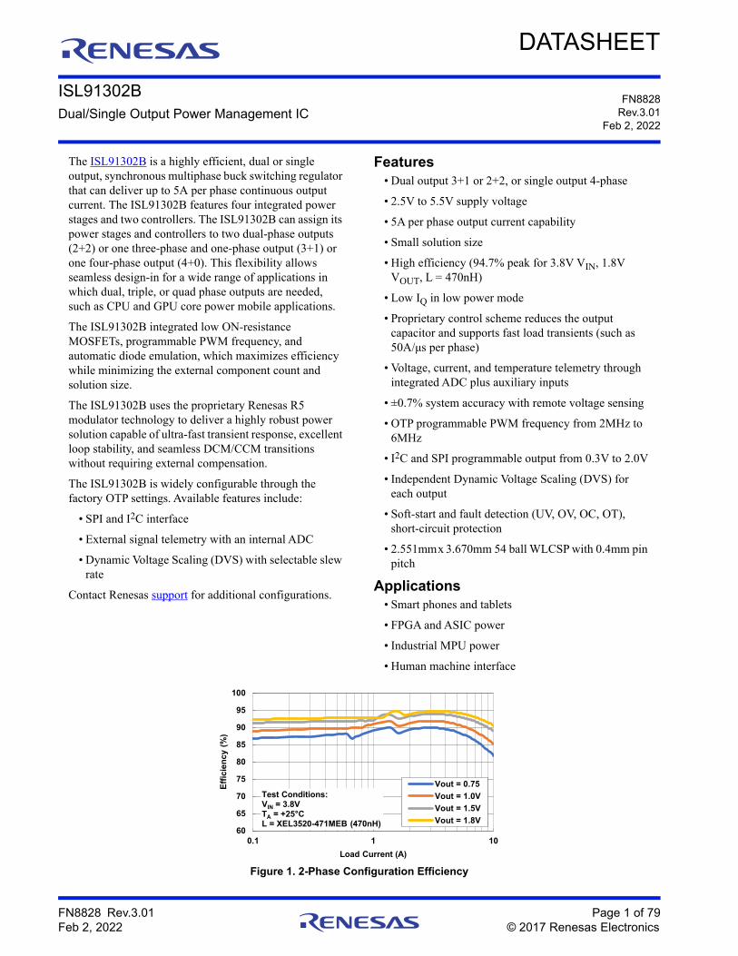
Figure 1. 2-Phase Configuration Efficiency
60
65
70
75
80
85
90
95
100
0.1 1 10
Effic
ienc
y (%
)
Load Current (A)
Vout = 0.75Vout = 1.0VVout = 1.5VVout = 1.8V
Test Conditions:VIN = 3.8VTA = +25°CL = XEL3520-471MEB (470nH)
FN8828 Rev.3.01 Page 2 of 79Feb 2, 2022
ISL91302B
Contents
1. Overview. . . . . . . . . . . . . . . . . . . . . . . . . . . . . . . . . . . . . . . . . . . . . . . . . . . . . . . . . . . . . . . . . . . . . . . . 4
1.1 Typical Application Circuits . . . . . . . . . . . . . . . . . . . . . . . . . . . . . . . . . . . . . . . . . . . . . . . . . . . . . . . 4
1.2 Block Diagram . . . . . . . . . . . . . . . . . . . . . . . . . . . . . . . . . . . . . . . . . . . . . . . . . . . . . . . . . . . . . . . . . 6
1.3 Ordering Information . . . . . . . . . . . . . . . . . . . . . . . . . . . . . . . . . . . . . . . . . . . . . . . . . . . . . . . . . . . . 7
1.4 Pin Configuration . . . . . . . . . . . . . . . . . . . . . . . . . . . . . . . . . . . . . . . . . . . . . . . . . . . . . . . . . . . . . . . 8
1.5 Pin Descriptions. . . . . . . . . . . . . . . . . . . . . . . . . . . . . . . . . . . . . . . . . . . . . . . . . . . . . . . . . . . . . . . . 9
2. Specifications. . . . . . . . . . . . . . . . . . . . . . . . . . . . . . . . . . . . . . . . . . . . . . . . . . . . . . . . . . . . . . . . . . . 11
2.1 Absolute Maximum Ratings . . . . . . . . . . . . . . . . . . . . . . . . . . . . . . . . . . . . . . . . . . . . . . . . . . . . . . 11
2.2 Thermal Information. . . . . . . . . . . . . . . . . . . . . . . . . . . . . . . . . . . . . . . . . . . . . . . . . . . . . . . . . . . . 11
2.3 Recommended Operation Conditions . . . . . . . . . . . . . . . . . . . . . . . . . . . . . . . . . . . . . . . . . . . . . . 11
2.4 Analog Specifications . . . . . . . . . . . . . . . . . . . . . . . . . . . . . . . . . . . . . . . . . . . . . . . . . . . . . . . . . . 12
3. Output Configurations. . . . . . . . . . . . . . . . . . . . . . . . . . . . . . . . . . . . . . . . . . . . . . . . . . . . . . . . . . . . 15
4. Typical Operating Performance . . . . . . . . . . . . . . . . . . . . . . . . . . . . . . . . . . . . . . . . . . . . . . . . . . . . 18
5. Applications Information. . . . . . . . . . . . . . . . . . . . . . . . . . . . . . . . . . . . . . . . . . . . . . . . . . . . . . . . . . 21
5.1 Inductor Selection . . . . . . . . . . . . . . . . . . . . . . . . . . . . . . . . . . . . . . . . . . . . . . . . . . . . . . . . . . . . . 21
5.2 Output Capacitor Selection . . . . . . . . . . . . . . . . . . . . . . . . . . . . . . . . . . . . . . . . . . . . . . . . . . . . . . 21
5.3 Input Capacitor Selection. . . . . . . . . . . . . . . . . . . . . . . . . . . . . . . . . . . . . . . . . . . . . . . . . . . . . . . . 22
5.4 ADC Telemetry. . . . . . . . . . . . . . . . . . . . . . . . . . . . . . . . . . . . . . . . . . . . . . . . . . . . . . . . . . . . . . . . 22
5.5 Dynamic Voltage Scaling (DVS) . . . . . . . . . . . . . . . . . . . . . . . . . . . . . . . . . . . . . . . . . . . . . . . . . . 23
5.6 Configuring DVS Speed. . . . . . . . . . . . . . . . . . . . . . . . . . . . . . . . . . . . . . . . . . . . . . . . . . . . . . . . . 26
5.7 Output Voltage Setting. . . . . . . . . . . . . . . . . . . . . . . . . . . . . . . . . . . . . . . . . . . . . . . . . . . . . . . . . . 26
5.8 Power Sequencing. . . . . . . . . . . . . . . . . . . . . . . . . . . . . . . . . . . . . . . . . . . . . . . . . . . . . . . . . . . . . 26
5.9 Watchdog Time (WDOG_RST Pin) . . . . . . . . . . . . . . . . . . . . . . . . . . . . . . . . . . . . . . . . . . . . . . . . 28
5.10 Interrupt Pin . . . . . . . . . . . . . . . . . . . . . . . . . . . . . . . . . . . . . . . . . . . . . . . . . . . . . . . . . . . . . . . . . . 28
5.11 Decay Mode. . . . . . . . . . . . . . . . . . . . . . . . . . . . . . . . . . . . . . . . . . . . . . . . . . . . . . . . . . . . . . . . . . 29
6. Protection Features (Faults) . . . . . . . . . . . . . . . . . . . . . . . . . . . . . . . . . . . . . . . . . . . . . . . . . . . . . . . 30
6.1 Over-Temperature Protection . . . . . . . . . . . . . . . . . . . . . . . . . . . . . . . . . . . . . . . . . . . . . . . . . . . . 30
6.2 Overcurrent Protection Mode. . . . . . . . . . . . . . . . . . . . . . . . . . . . . . . . . . . . . . . . . . . . . . . . . . . . . 30
6.3 Overvoltage (OV)/Undervoltage (UV) Protection. . . . . . . . . . . . . . . . . . . . . . . . . . . . . . . . . . . . . . 30
7. Serial Communication Interface . . . . . . . . . . . . . . . . . . . . . . . . . . . . . . . . . . . . . . . . . . . . . . . . . . . . 31
7.1 SPI Serial Interface . . . . . . . . . . . . . . . . . . . . . . . . . . . . . . . . . . . . . . . . . . . . . . . . . . . . . . . . . . . . 31
7.2 I2C Interface. . . . . . . . . . . . . . . . . . . . . . . . . . . . . . . . . . . . . . . . . . . . . . . . . . . . . . . . . . . . . . . . . . 34
8. Board Layout Recommendations. . . . . . . . . . . . . . . . . . . . . . . . . . . . . . . . . . . . . . . . . . . . . . . . . . . 38
8.1 PCB Layout Summary . . . . . . . . . . . . . . . . . . . . . . . . . . . . . . . . . . . . . . . . . . . . . . . . . . . . . . . . . . 40
8.2 PCB Design for WLCSP Recommendations . . . . . . . . . . . . . . . . . . . . . . . . . . . . . . . . . . . . . . . . . 40
FN8828 Rev.3.01 Page 3 of 79Feb 2, 2022
ISL91302B
9. Register Address Map . . . . . . . . . . . . . . . . . . . . . . . . . . . . . . . . . . . . . . . . . . . . . . . . . . . . . . . . . . . . 41
10. Register Description by Address . . . . . . . . . . . . . . . . . . . . . . . . . . . . . . . . . . . . . . . . . . . . . . . . . . . 42
11. Revision History. . . . . . . . . . . . . . . . . . . . . . . . . . . . . . . . . . . . . . . . . . . . . . . . . . . . . . . . . . . . . . . . . 78
12. Package Outline Drawing . . . . . . . . . . . . . . . . . . . . . . . . . . . . . . . . . . . . . . . . . . . . . . . . . . . . . . . . . 79
FN8828 Rev.3.01 Page 4 of 79Feb 2, 2022
ISL91302B 1. Overview
1. Overview
1.1 Typical Application Circuits
Figure 2. Typical Application 4-Phase Single Output
Figure 3. Typical Application Circuit: 3-Phase + 1-Phase
AVIN
PVIN_A
EN
2.5V to 5.5V
VOUT1
VOUT1
PH_D
PH_B
RTN1
VIO
AVIN_FILT
PH_C
VOUT2
GND
RTN2
INTMPIO<3:0>
4
WDOG_RSTGPIO<1:0>
2
PVIN_B
PVIN_C
PVIN_D
PGND_CDPGND_AB
ISL91302B
1.8V
1.5V to 5.5V
2.5V to 5.5V
PH_A
AVIN
PVIN_A
EN
2.5V to 5.5V
VOUT1
VOUT1
PH_D
PH_B
RTN1
VIO
AVIN_FILT
VOUT2PH_C
VOUT2
GND
RTN2
INTMPIO<3:0>
4
WDOG_RSTGPIO<1:0>
2
PVIN_B
PVIN_C
PVIN_D
PGND_CDPGND_AB
ISL91302B
1.8V
1.5V to 5.5V
2.5V to 5.5V
PH_A
FN8828 Rev.3.01 Page 5 of 79Feb 2, 2022
ISL91302B 1. Overview
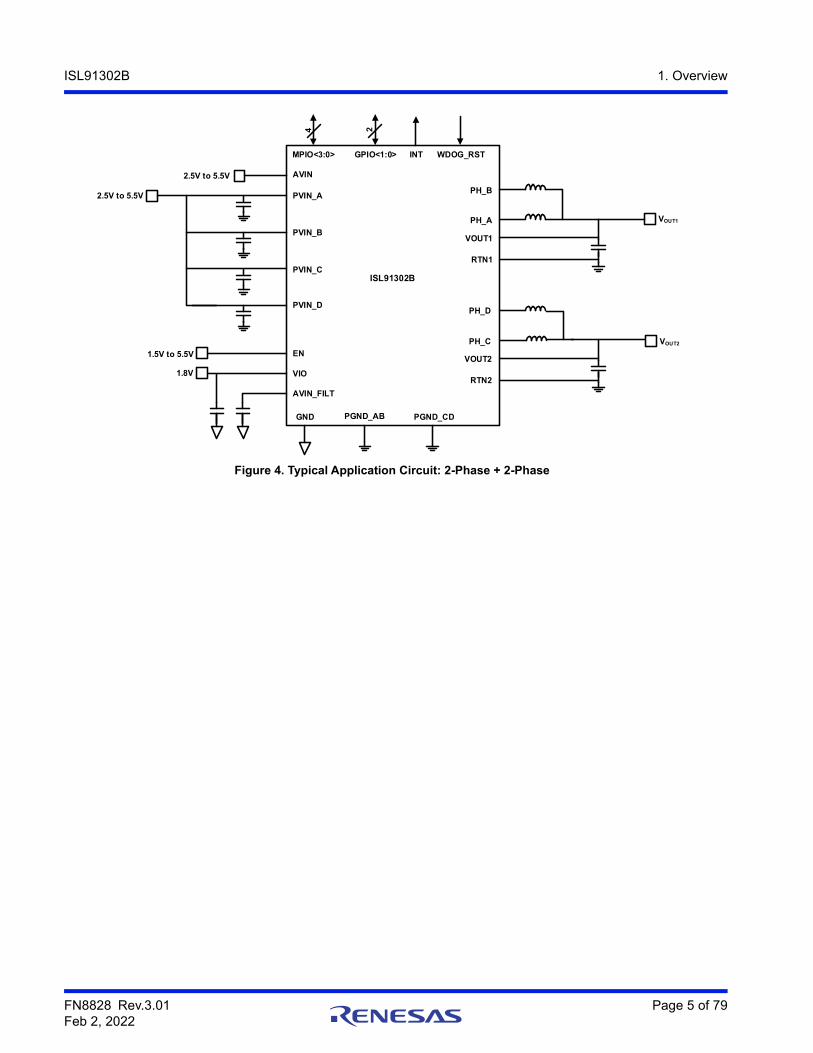
Figure 4. Typical Application Circuit: 2-Phase + 2-Phase
AVIN
PVIN_A
EN
2.5V to 5.5V
VOUT1
VOUT1
PH_B
PH_A
RTN1
VIO
AVIN_FILT
VOUT2
PH_D
PH_C
VOUT2
GND
RTN2
INTMPIO<3:0>
4
WDOG_RSTGPIO<1:0>
2
PVIN_B
PVIN_C
PVIN_D
PGND_CDPGND_AB
ISL91302B
1.8V
1.5V to 5.5V
2.5V to 5.5V
FN8828 Rev.3.01 Page 6 of 79Feb 2, 2022
ISL91302B 1. Overview
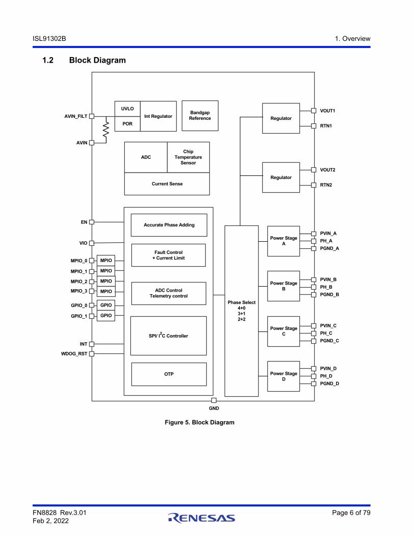
1.2 Block Diagram
Figure 5. Block Diagram
Int RegulatorBandgap Reference Regulator
Power Stage A
Power Stage B
Power Stage C
Power Stage D
VOUT1
RTN1
PGND_A
PH_A
PVIN_A
Chip Temperature
SensorADC
VIO
EN
MPIO
MPIO
MPIO
MPIO_0
SPI/ I2C Controller
AVIN_FILT
ADC ControlTelemetry control
Fault Control+ Current Limit
Accurate Phase Adding
GND
UVLO
POR
MPIO_1
MPIO_2
AVIN
OTP
Regulator
VOUT2
RTN2
Phase Select4+03+12+2
PGND_B
PH_B
PVIN_B
PGND_C
PH_C
PVIN_C
PGND_D
PH_D
PVIN_D
Current Sense
MPIOMPIO_3
INT
WDOG_RST
GPIO
GPIO
GPIO_0
GPIO_1
FN8828 Rev.3.01 Page 7 of 79Feb 2, 2022
ISL91302B 1. Overview
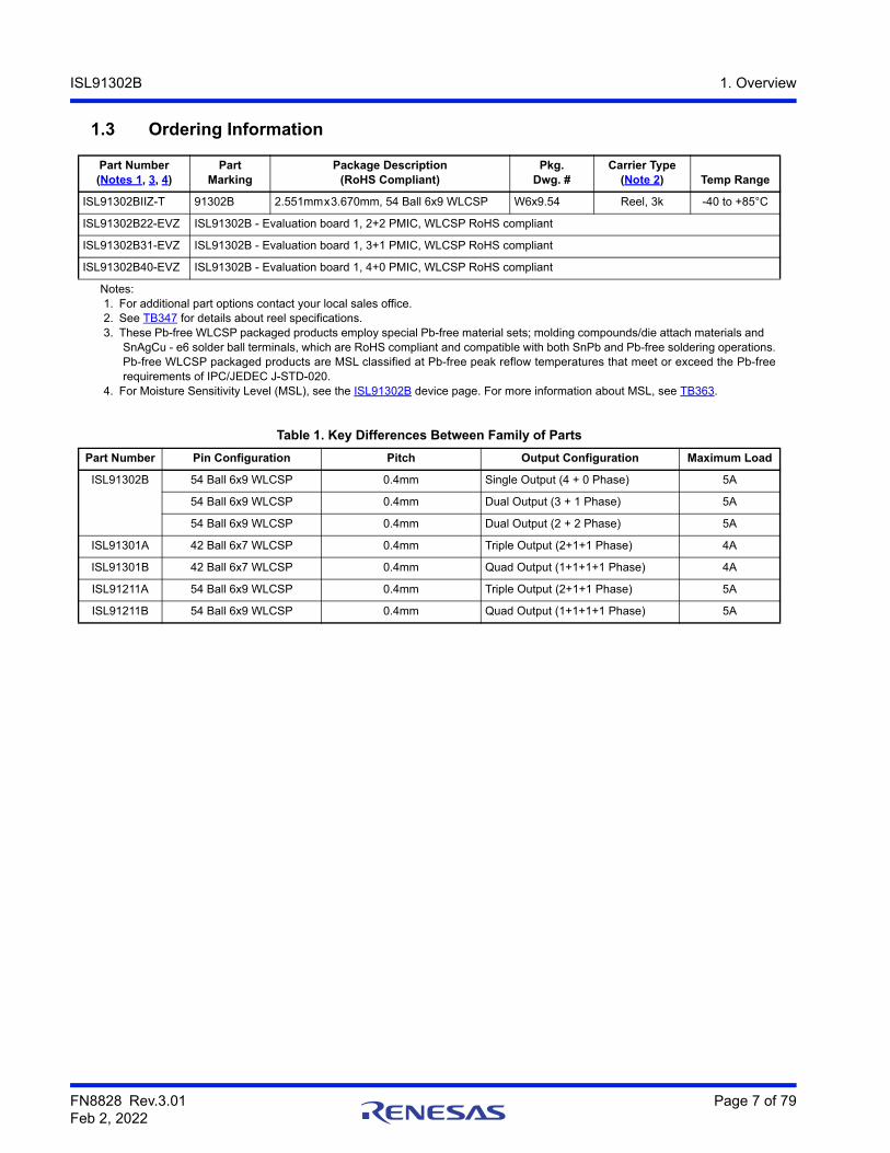
1.3 Ordering Information
Part Number(Notes 1, 3, 4)
PartMarking
Package Description(RoHS Compliant)
Pkg.Dwg. #
Carrier Type (Note 2) Temp Range
ISL91302BIIZ-T 91302B 2.551mmx3.670mm, 54 Ball 6x9 WLCSP W6x9.54 Reel, 3k -40 to +85°C
ISL91302B22-EVZ ISL91302B - Evaluation board 1, 2+2 PMIC, WLCSP RoHS compliant
ISL91302B31-EVZ ISL91302B - Evaluation board 1, 3+1 PMIC, WLCSP RoHS compliant
ISL91302B40-EVZ ISL91302B - Evaluation board 1, 4+0 PMIC, WLCSP RoHS compliant
Notes:1. For additional part options contact your local sales office.2. See TB347 for details about reel specifications.3. These Pb-free WLCSP packaged products employ special Pb-free material sets; molding compounds/die attach materials and
SnAgCu - e6 solder ball terminals, which are RoHS compliant and compatible with both SnPb and Pb-free soldering operations.Pb-free WLCSP packaged products are MSL classified at Pb-free peak reflow temperatures that meet or exceed the Pb-freerequirements of IPC/JEDEC J-STD-020.
4. For Moisture Sensitivity Level (MSL), see the ISL91302B device page. For more information about MSL, see TB363.
Table 1. Key Differences Between Family of Parts
Part Number Pin Configuration Pitch Output Configuration Maximum Load
ISL91302B 54 Ball 6x9 WLCSP 0.4mm Single Output (4 + 0 Phase) 5A
54 Ball 6x9 WLCSP 0.4mm Dual Output (3 + 1 Phase) 5A
54 Ball 6x9 WLCSP 0.4mm Dual Output (2 + 2 Phase) 5A
ISL91301A 42 Ball 6x7 WLCSP 0.4mm Triple Output (2+1+1 Phase) 4A
ISL91301B 42 Ball 6x7 WLCSP 0.4mm Quad Output (1+1+1+1 Phase) 4A
ISL91211A 54 Ball 6x9 WLCSP 0.4mm Triple Output (2+1+1 Phase) 5A
ISL91211B 54 Ball 6x9 WLCSP 0.4mm Quad Output (1+1+1+1 Phase) 5A
FN8828 Rev.3.01 Page 8 of 79Feb 2, 2022
ISL91302B 1. Overview
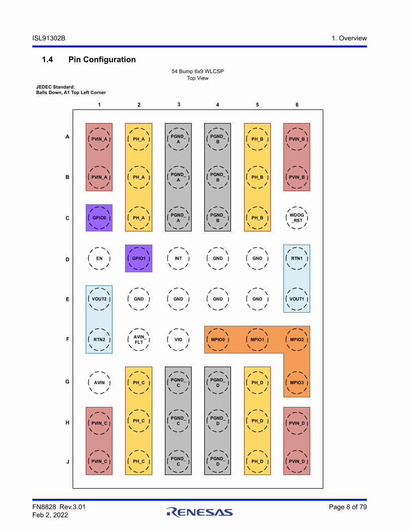
1.4 Pin Configuration54 Bump 6x9 WLCSP
Top View
JEDEC Standard: Balls Down, A1 Top Left Corner
A
B
C
D
E
1 2 3 4 5
F
G
6
PVIN_A
PVIN_A
PH_A
PH_A
PH_A
PGND_A
PGND_A
PGND_A
PGND_B
PGND_B
PGND_B
PH_B
PH_B
PH_B
PVIN_B
PVIN_B
PVIN_C
PVIN_C
PH_C
PH_C
PH_C
PGND_C
PGND_C
PGND_C
PGND_D
PGND_D
PGND_D
PH_D
PH_D
PH_D
PVIN_D
PVIN_D
H
J
AVIN
RTN2
VOUT2
AVIN_ FLT
VIO MPIO0 MPIO1 MPIO2
MPIO3
VOUT1
RTN1
GND GND GND GND
GND GNDINTGPIO1
GPIO0
EN
WDOG_RST
FN8828 Rev.3.01 Page 9 of 79Feb 2, 2022
ISL91302B 1. Overview
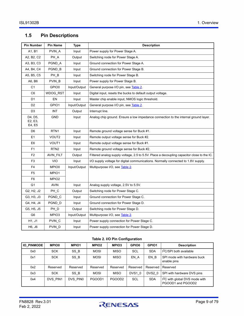
1.5 Pin Descriptions
Pin Number Pin Name Type Description
A1, B1 PVIN_A Input Power supply for Power Stage A.
A2, B2, C2 PH_A Output Switching node for Power Stage A.
A3, B3, C3 PGND_A Input Ground connection for Power Stage A.
A4, B4, C4 PGND_B Input Ground connection for Power Stage B.
A5, B5, C5 PH_B Input Switching node for Power Stage B.
A6, B6 PVIN_B Input Power supply for Power Stage B.
C1 GPIO0 Input/Output General purpose I/O pin, see Table 2.
C6 WDOG_RST Input Digital input, resets the bucks to default output voltage.
D1 EN Input Master chip enable input, NMOS logic threshold.
D2 GPIO1 Input/Output General purpose I/O pin, see Table 2.
D3 INT Output Interrupt line.
D4, D5,E2, E3, E4, E5
GND Input Analog chip ground. Ensure a low impedance connection to the internal ground layer.
D6 RTN1 Input Remote ground voltage sense for Buck #1.
E1 VOUT2 Input Remote output voltage sense for Buck #2.
E6 VOUT1 Input Remote output voltage sense for Buck #1.
F1 RTN2 Input Remote ground voltage sense for Buck #2.
F2 AVIN_FILT Output Filtered analog supply voltage, 2.5 to 5.5V. Place a decoupling capacitor close to the IC.
F3 VIO Input I/O supply voltage for digital communications. Normally connected to 1.8V supply.
F4 MPIO0 Input/Output Multipurpose I/O, see Table 2.
F5 MPIO1
F6 MPIO2
G1 AVIN Input Analog supply voltage, 2.5V to 5.5V.
G2, H2, J2 PH_C Output Switching node for Power Stage C.
G3, H3, J3 PGND_C Input Ground connection for Power Stage C.
G4, H4, J4 PGND_D Input Ground connection for Power Stage D.
G5, H5, J5 PH_D Output Switching node for Power Stage D.
G6 MPIO3 Input/Output Multipurpose I/O, see Table 2.
H1, J1 PVIN_C Input Power supply connection for Power Stage C.
H6, J6 PVIN_D Input Power supply connection for Power Stage D.
Table 2. I/O Pin Configuration
IO_PINMODE MPIO0 MPIO1 MPIO2 MPIO3 GPIO0 GPIO1 Description
0x0 SCK SS_B MOSI MISO SCL SDA I2C/SPI both available
0x1 SCK SS_B MOSI MISO EN_A EN_B SPI mode with hardware buck enable pins
0x2 Reserved Reserved Reserved Reserved Reserved Reserved Reserved
0x3 SCK SS_B MOSI MISO DVS1_0 DVS2_0 SPI with hardware DVS pins
0x4 DVS_PIN1 DVS_PIN0 PGOOD1 PGOOD2 SCL SDA I2C with global DVS mode with PGOOD1 and PGOOD2
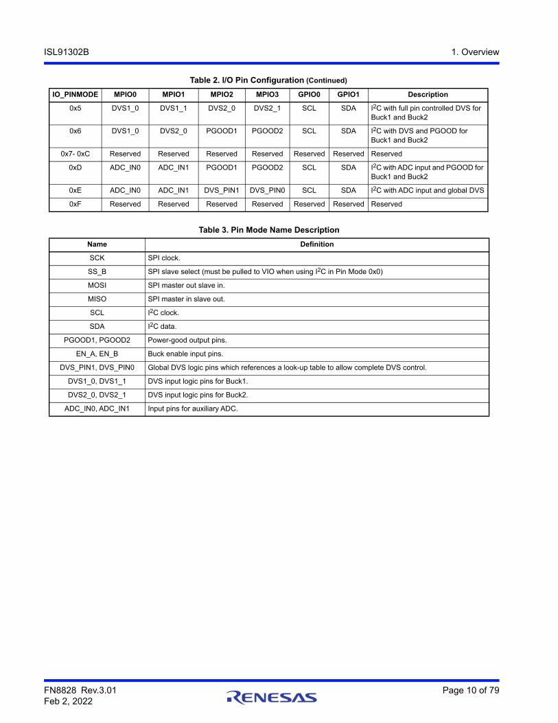
FN8828 Rev.3.01 Page 10 of 79Feb 2, 2022
ISL91302B 1. Overview
0x5 DVS1_0 DVS1_1 DVS2_0 DVS2_1 SCL SDA I2C with full pin controlled DVS for Buck1 and Buck2
0x6 DVS1_0 DVS2_0 PGOOD1 PGOOD2 SCL SDA I2C with DVS and PGOOD for Buck1 and Buck2
0x7- 0xC Reserved Reserved Reserved Reserved Reserved Reserved Reserved
0xD ADC_IN0 ADC_IN1 PGOOD1 PGOOD2 SCL SDA I2C with ADC input and PGOOD for Buck1 and Buck2
0xE ADC_IN0 ADC_IN1 DVS_PIN1 DVS_PIN0 SCL SDA I2C with ADC input and global DVS
0xF Reserved Reserved Reserved Reserved Reserved Reserved Reserved
Table 3. Pin Mode Name Description
Name Definition
SCK SPI clock.
SS_B SPI slave select (must be pulled to VIO when using I2C in Pin Mode 0x0)
MOSI SPI master out slave in.
MISO SPI master in slave out.
SCL I2C clock.
SDA I2C data.
PGOOD1, PGOOD2 Power-good output pins.
EN_A, EN_B Buck enable input pins.
DVS_PIN1, DVS_PIN0 Global DVS logic pins which references a look-up table to allow complete DVS control.
DVS1_0, DVS1_1 DVS input logic pins for Buck1.
DVS2_0, DVS2_1 DVS input logic pins for Buck2.
ADC_IN0, ADC_IN1 Input pins for auxiliary ADC.
Table 2. I/O Pin Configuration (Continued)
IO_PINMODE MPIO0 MPIO1 MPIO2 MPIO3 GPIO0 GPIO1 Description
FN8828 Rev.3.01 Page 11 of 79Feb 2, 2022
ISL91302B 2. Specifications
2. Specifications
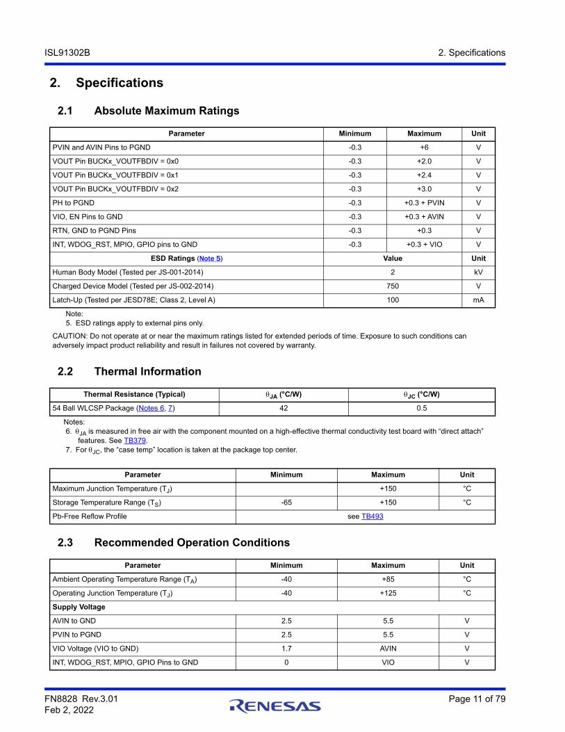
2.1 Absolute Maximum Ratings
2.2 Thermal Information
2.3 Recommended Operation Conditions
Parameter Minimum Maximum Unit
PVIN and AVIN Pins to PGND -0.3 +6 V
VOUT Pin BUCKx_VOUTFBDIV = 0x0 -0.3 +2.0 V
VOUT Pin BUCKx_VOUTFBDIV = 0x1 -0.3 +2.4 V
VOUT Pin BUCKx_VOUTFBDIV = 0x2 -0.3 +3.0 V
PH to PGND -0.3 +0.3 + PVIN V
VIO, EN Pins to GND -0.3 +0.3 + AVIN V
RTN, GND to PGND Pins -0.3 +0.3 V
INT, WDOG_RST, MPIO, GPIO pins to GND -0.3 +0.3 + VIO V
ESD Ratings (Note 5) Value Unit
Human Body Model (Tested per JS-001-2014) 2 kV
Charged Device Model (Tested per JS-002-2014) 750 V
Latch-Up (Tested per JESD78E; Class 2, Level A) 100 mA
Note:5. ESD ratings apply to external pins only.
CAUTION: Do not operate at or near the maximum ratings listed for extended periods of time. Exposure to such conditions can adversely impact product reliability and result in failures not covered by warranty.
Thermal Resistance (Typical) JA (°C/W) JC (°C/W)
54 Ball WLCSP Package (Notes 6, 7) 42 0.5
Notes:6. JA is measured in free air with the component mounted on a high-effective thermal conductivity test board with “direct attach”
features. See TB379.7. For JC, the “case temp” location is taken at the package top center.
Parameter Minimum Maximum Unit
Maximum Junction Temperature (TJ) +150 °C
Storage Temperature Range (TS) -65 +150 °C
Pb-Free Reflow Profile see TB493
Parameter Minimum Maximum Unit
Ambient Operating Temperature Range (TA) -40 +85 °C
Operating Junction Temperature (TJ) -40 +125 °C
Supply Voltage
AVIN to GND 2.5 5.5 V
PVIN to PGND 2.5 5.5 V
VIO Voltage (VIO to GND) 1.7 AVIN V
INT, WDOG_RST, MPIO, GPIO Pins to GND 0 VIO V
FN8828 Rev.3.01 Page 12 of 79Feb 2, 2022
ISL91302B 2. Specifications
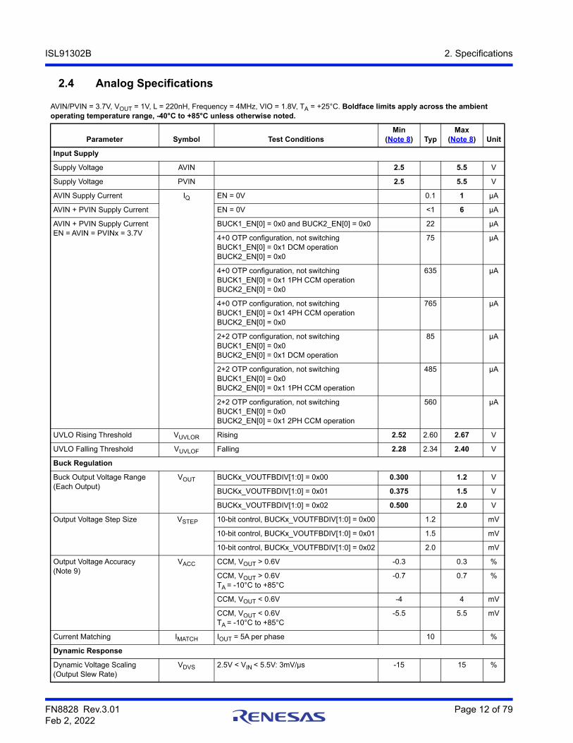
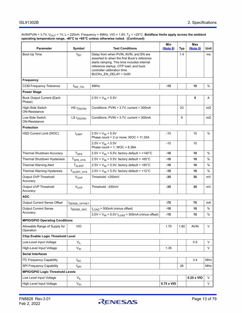
2.4 Analog Specifications
AVIN/PVIN = 3.7V, VOUT = 1V, L = 220nH, Frequency = 4MHz, VIO = 1.8V, TA = +25°C. Boldface limits apply across the ambient operating temperature range, -40°C to +85°C unless otherwise noted.
Parameter Symbol Test ConditionsMin
(Note 8) TypMax
(Note 8) Unit
Input Supply
Supply Voltage AVIN 2.5 5.5 V
Supply Voltage PVIN 2.5 5.5 V
AVIN Supply Current IQ EN = 0V 0.1 1 µA
AVIN + PVIN Supply Current EN = 0V <1 6 µA
AVIN + PVIN Supply CurrentEN = AVIN = PVINx = 3.7V
BUCK1_EN[0] = 0x0 and BUCK2_EN[0] = 0x0 22 µA
4+0 OTP configuration, not switchingBUCK1_EN[0] = 0x1 DCM operationBUCK2_EN[0] = 0x0
75 µA
4+0 OTP configuration, not switchingBUCK1_EN[0] = 0x1 1PH CCM operationBUCK2_EN[0] = 0x0
635 µA
4+0 OTP configuration, not switchingBUCK1_EN[0] = 0x1 4PH CCM operationBUCK2_EN[0] = 0x0
765 µA
2+2 OTP configuration, not switchingBUCK1_EN[0] = 0x0BUCK2_EN[0] = 0x1 DCM operation
85 µA
2+2 OTP configuration, not switchingBUCK1_EN[0] = 0x0BUCK2_EN[0] = 0x1 1PH CCM operation
485 µA
2+2 OTP configuration, not switchingBUCK1_EN[0] = 0x0BUCK2_EN[0] = 0x1 2PH CCM operation
560 µA
UVLO Rising Threshold VUVLOR Rising 2.52 2.60 2.67 V
UVLO Falling Threshold VUVLOF Falling 2.28 2.34 2.40 V
Buck Regulation
Buck Output Voltage Range(Each Output)
VOUT BUCKx_VOUTFBDIV[1:0] = 0x00 0.300 1.2 V
BUCKx_VOUTFBDIV[1:0] = 0x01 0.375 1.5 V
BUCKx_VOUTFBDIV[1:0] = 0x02 0.500 2.0 V
Output Voltage Step Size VSTEP 10-bit control, BUCKx_VOUTFBDIV[1:0] = 0x00 1.2 mV
10-bit control, BUCKx_VOUTFBDIV[1:0] = 0x01 1.5 mV
10-bit control, BUCKx_VOUTFBDIV[1:0] = 0x02 2.0 mV
Output Voltage Accuracy (Note 9)
VACC CCM, VOUT > 0.6V -0.3 0.3 %
CCM, VOUT > 0.6VTA = -10°C to +85°C
-0.7 0.7 %
CCM, VOUT < 0.6V -4 4 mV
CCM, VOUT < 0.6VTA = -10°C to +85°C
-5.5 5.5 mV
Current Matching IMATCH IOUT = 5A per phase 10 %
Dynamic Response
Dynamic Voltage Scaling (Output Slew Rate)
VDVS 2.5V < VIN < 5.5V: 3mV/µs -15 15 %
FN8828 Rev.3.01 Page 13 of 79Feb 2, 2022
ISL91302B 2. Specifications
Boot-Up Time VBT Delay from when PVIN, AVIN, and EN are asserted to when the first Buck’s reference starts ramping. This time includes internal reference startup, OTP load, and buck controller calibration time. BUCKx_EN_DELAY = 0x00
1.4 ms
Frequency
CCM Frequency Tolerance fSW_TOL 4MHz -15 15 %
Power Stage
Buck Output Current (Each Phase)
2.5V < VIN < 5.5V 5 A
High-Side Switch ON-Resistance
HS rDS(ON) Conditions: PVIN = 3.7V, current = 300mA 23 mΩ
Low-Side Switch ON-Resistance
LS rDS(ON) Conditions: PVIN = 3.7V, current = 300mA 9 mΩ
Protection
HSD Current Limit (WOC) ILIMIT 2.5V < VIN < 5.5VPhase count = 2 or more; WOC = 11.35A
-10 10 %
2.5V < VIN < 5.5VPhase count = 1; WOC = 8.38A
-10 10
Thermal Shutdown Accuracy TSPS 2.5V < VIN < 5.5V, factory default = +140°C -10 10 %
Thermal Shutdown Hysteresis TSPS_HYS 2.5V < VIN < 5.5V, factory default = +60°C -10 10 %
Thermal Warning Alert TALERT 2.5V < VIN < 5.5V, factory default = +85°C -10 10 %
Thermal Warning Hysteresis TALERT_HYS 2.5V < VIN < 5.5V, factory default = +12°C -10 10 %
Output OVP Threshold Accuracy
VOVP Threshold: +250mV -35 35 mV
Output UVP Threshold Accuracy
VUVP Threshold: -250mV -35 35 mV
ADC
Output Current Sense Offset ISENSE_OFFSET -75 75 mA
Output Current Sense Accuracy
ISENSE_ADC ILOAD = 500mA (minus offset) -10 10 %
3.0V < VIN < 5.0V ILOAD = 500mA (minus offset) -15 15 %
MPIO/GPIO Operating Conditions
Allowable Range of Supply for Operation
VIO 1.70 1.80 AVIN V
Chip Enable Logic Threshold Level
Low-Level Input Voltage VIL 0.5 V
High-Level Input Voltage VIH 1.35 V
Serial Interfaces
I2C Frequency Capability fI2C 3.4 MHz
SPI Frequency Capability fSPI 26 MHz
MPIO/GPIO Logic Threshold Levels
Low Level Input Voltage VIL 0.25 x VIO V
High Level Input Voltage VIH 0.75 x VIO V
AVIN/PVIN = 3.7V, VOUT = 1V, L = 220nH, Frequency = 4MHz, VIO = 1.8V, TA = +25°C. Boldface limits apply across the ambient operating temperature range, -40°C to +85°C unless otherwise noted. (Continued)
Parameter Symbol Test ConditionsMin
(Note 8) TypMax
(Note 8) Unit
FN8828 Rev.3.01 Page 14 of 79Feb 2, 2022
ISL91302B 2. Specifications
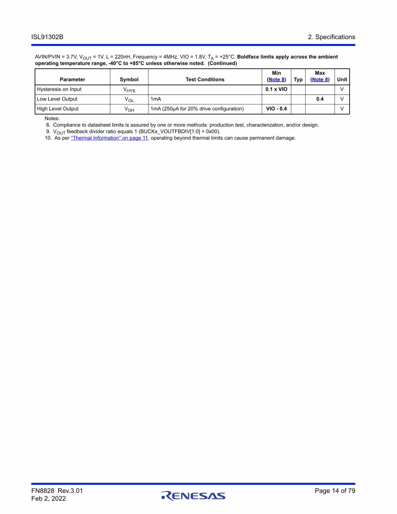
Hysteresis on Input VHYS 0.1 x VIO V
Low Level Output VOL 1mA 0.4 V
High Level Output VOH 1mA (250µA for 20% drive configuration) VIO - 0.4 V
Notes:8. Compliance to datasheet limits is assured by one or more methods: production test, characterization, and/or design.9. VOUT feedback divider ratio equals 1 (BUCKx_VOUTFBDIV[1:0] = 0x00).
10. As per “Thermal Information” on page 11, operating beyond thermal limits can cause permanent damage.
AVIN/PVIN = 3.7V, VOUT = 1V, L = 220nH, Frequency = 4MHz, VIO = 1.8V, TA = +25°C. Boldface limits apply across the ambient operating temperature range, -40°C to +85°C unless otherwise noted. (Continued)
Parameter Symbol Test ConditionsMin
(Note 8) TypMax
(Note 8) Unit
FN8828 Rev.3.01 Page 15 of 79Feb 2, 2022
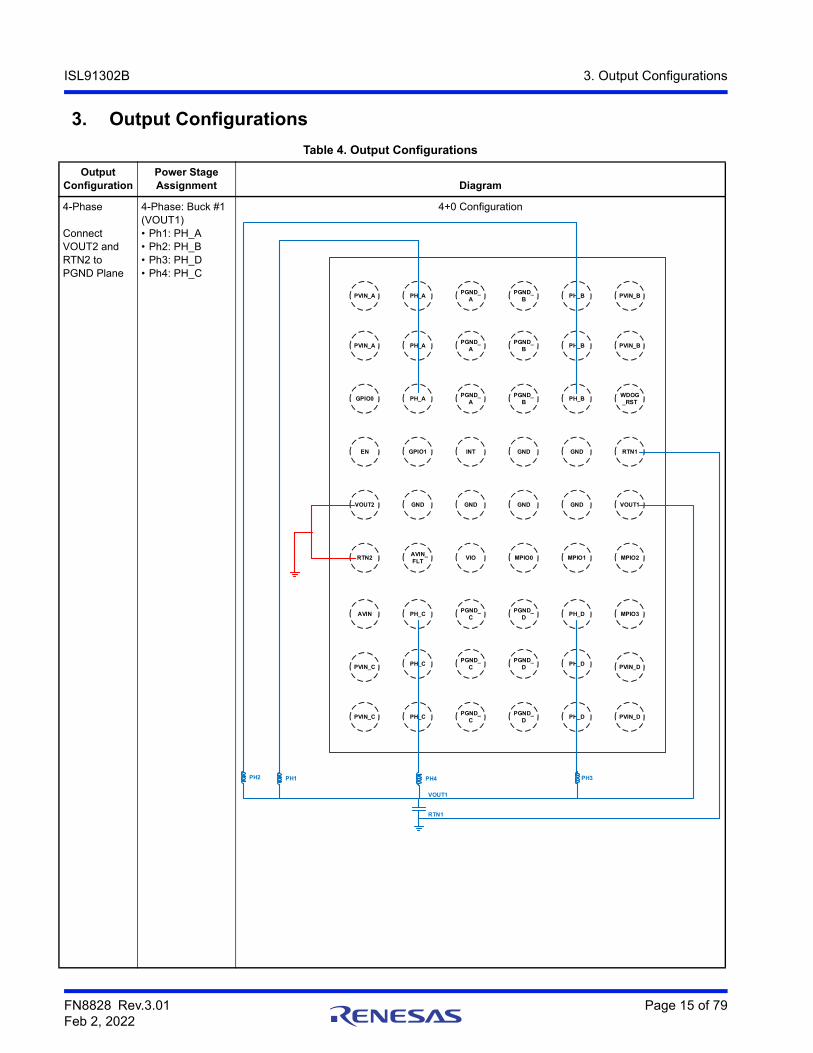
ISL91302B 3. Output Configurations
3. Output Configurations
Table 4. Output Configurations
OutputConfiguration
Power StageAssignment Diagram
4-Phase
ConnectVOUT2 andRTN2 to PGND Plane
4-Phase: Buck #1(VOUT1)• Ph1: PH_A• Ph2: PH_B• Ph3: PH_D• Ph4: PH_C
4+0 Configuration
PVIN_A
PVIN_A
PH_A
PH_A
PH_A
PGND_A
PGND_A
PGND_A
PGND_B
PGND_B
PGND_B
PH_B
PH_B
PH_B
PVIN_B
PVIN_B
PVIN_C
PVIN_C
PH_C
PH_C
PH_C
PGND_C
PGND_C
PGND_C
PGND_D
PGND_D
PGND_D
PH_D
PH_D
PH_D
PVIN_D
PVIN_D
AVIN
RTN2
VOUT2
AVIN_ FLT
VIO MPIO0 MPIO1 MPIO2
MPIO3
VOUT1
RTN1
GND GND GND GND
GND GNDINTGPIO1
GPIO0
EN
WDOG_RST
VOUT1
RTN1
PH2 PH4PH1 PH3

FN8828 Rev.3.01 Page 16 of 79Feb 2, 2022
ISL91302B 3. Output Configurations
3-Phase +1-Phase
3+1 Configuration:• 3-phase: Buck #1
(VOUT1)Ph1: PH_APh2: PH_BPh3: PH_D
• 1-phase: Buck #2(VOUT2)Ph1: PH_C
3+1 Configuration
Table 4. Output Configurations (Continued)
OutputConfiguration
Power StageAssignment Diagram
PVIN_A
PVIN_A
PH_A
PH_A
PH_A
PGND_A
PGND_A
PGND_A
PGND_B
PGND_B
PGND_B
PH_B
PH_B
PH_B
PVIN_B
PVIN_B
PVIN_C
PVIN_C
PH_C
PH_C
PH_C
PGND_C
PGND_C
PGND_C
PGND_D
PGND_D
PGND_D
PH_D
PH_D
PH_D
PVIN_D
PVIN_D
AVIN
RTN2
VOUT2
AVIN_ FLT
VIO MPIO0 MPIO1 MPIO2
MPIO3
VOUT1
RTN1
GND GND GND GND
GND GNDINTGPIO1
GPIO0
EN
WDOG_RST
VOUT1
RTN1
PH2 PH1 PH3
VOUT2
RTN
2
FN8828 Rev.3.01 Page 17 of 79Feb 2, 2022
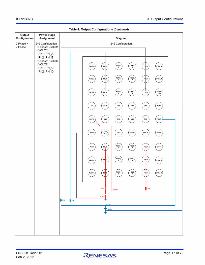
ISL91302B 3. Output Configurations
2-Phase +2-Phase
2+2 Configuration• 2-phase: Buck #1
(VOUT1)Ph1: PH_APh2: PH_B
• 2-phase: Buck #2(VOUT2)Ph1: PH_CPh2: PH_D
2+2 Configuration
Table 4. Output Configurations (Continued)
OutputConfiguration
Power StageAssignment Diagram
PVIN_A
PVIN_A
PH_A
PH_A
PH_A
PGND_A
PGND_A
PGND_A
PGND_B
PGND_B
PGND_B
PH_B
PH_B
PH_B
PVIN_B
PVIN_B
PVIN_C
PVIN_C
PH_C
PH_C
PH_C
PGND_C
PGND_C
PGND_C
PGND_D
PGND_D
PGND_D
PH_D
PH_D
PH_D
PVIN_D
PVIN_D
AVIN
RTN2
VOUT2
AVIN_ FLT
VIO MPIO0 MPIO1 MPIO2
MPIO3
VOUT1
RTN1
GND GND GND GND
GND GNDINTGPIO1
GPIO0
EN
WDOG_RST
VOUT1
RTN1
PH2 PH1
PH2VOUT2
RTN2
PH1
FN8828 Rev.3.01 Page 18 of 79Feb 2, 2022
ISL91302B 4. Typical Operating Performance
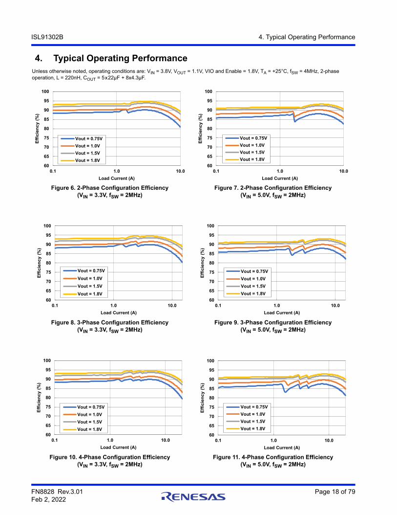
4. Typical Operating PerformanceUnless otherwise noted, operating conditions are: VIN = 3.8V, VOUT = 1.1V, VIO and Enable = 1.8V, TA = +25°C, fSW = 4MHz, 2-phase operation, L = 220nH, COUT = 5x22µF + 8x4.3µF.
Figure 6. 2-Phase Configuration Efficiency(VIN = 3.3V, fSW = 2MHz)
Figure 7. 2-Phase Configuration Efficiency(VIN = 5.0V, fSW = 2MHz)
Figure 8. 3-Phase Configuration Efficiency(VIN = 3.3V, fSW = 2MHz)
Figure 9. 3-Phase Configuration Efficiency(VIN = 5.0V, fSW = 2MHz)
Figure 10. 4-Phase Configuration Efficiency(VIN = 3.3V, fSW = 2MHz)
Figure 11. 4-Phase Configuration Efficiency(VIN = 5.0V, fSW = 2MHz)
60
65
70
75
80
85
90
95
100
0.1 1.0 10.0
Effic
ienc
y (%
)
Load Current (A)
Vout = 0.75VVout = 1.0VVout = 1.5VVout = 1.8V
60
65
70
75
80
85
90
95
100
0.1 1.0 10.0
Effic
ienc
y (%
)
Load Current (A)
Vout = 0.75VVout = 1.0VVout = 1.5VVout = 1.8V
60
65
70
75
80
85
90
95
100
0.1 1.0 10.0
Effic
ienc
y (%
)
Load Current (A)
Vout = 0.75VVout = 1.0VVout = 1.5VVout = 1.8V
60
65
70
75
80
85
90
95
100
0.1 1.0 10.0
Effic
ienc
y (%
)
Load Current (A)
Vout = 0.75VVout = 1.0VVout = 1.5VVout = 1.8V
60
65
70
75
80
85
90
95
100
0.1 1.0 10.0
Effic
ienc
y (%
)
Load Current (A)
Vout = 0.75VVout = 1.0VVout = 1.5VVout = 1.8V
60
65
70
75
80
85
90
95
100
0.1 1.0 10.0
Effic
ienc
y (%
)
Load Current (A)
Vout = 0.75VVout = 1.0VVout = 1.5VVout = 1.8V
FN8828 Rev.3.01 Page 19 of 79Feb 2, 2022
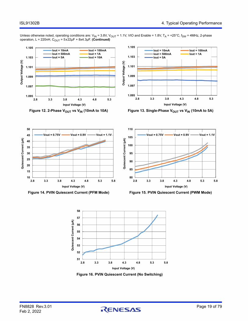
ISL91302B 4. Typical Operating Performance
Figure 12. 2-Phase VOUT vs VIN (10mA to 10A) Figure 13. Single-Phase VOUT vs VIN (10mA to 5A)
Figure 14. PVIN Quiescent Current (PFM Mode) Figure 15. PVIN Quiescent Current (PWM Mode)
Figure 16. PVIN Quiescent Current (No Switching)
Unless otherwise noted, operating conditions are: VIN = 3.8V, VOUT = 1.1V, VIO and Enable = 1.8V, TA = +25°C, fSW = 4MHz, 2-phase operation, L = 220nH, COUT = 5x22µF + 8x4.3µF. (Continued)
1.095
1.097
1.099
1.101
1.103
1.105
2.8 3.3 3.8 4.3 4.8 5.3
Input Voltage (V)
Iout = 10mA Iout = 100mAIout = 500mA Iout = 1AIout = 5A Iout = 10A
Ou
tpu
t V
olt
ag
e (
V)
1.095
1.097
1.099
1.101
1.103
1.105
2.8 3.3 3.8 4.3 4.8 5.3
Input Voltage (V)
Iout = 10mA Iout = 100mAIout = 500mA Iout = 1AIout = 5A
Ou
tpu
t V
olt
age
(V)
10
15
20
25
30
35
40
45
50
2.8 3.3 3.8 4.3 4.8 5.3 5.8
Input Voltage (V)
Vout = 0.75V Vout = 0.9V Vout = 1.1V
Qu
ies
cen
t C
urr
en
t (µ
A)
80
85
90
95
100
105
110
2.8 3.3 3.8 4.3 4.8 5.3 5.8
Input Voltage (V)
Vout = 0.75V Vout = 0.9V Vout = 1.1V
Qu
ies
ce
nt
Cu
rre
nt
(µA
)
51
52
53
54
55
56
57
58
2.8 3.3 3.8 4.3 4.8 5.3 5.8
Input Voltage (V)
Qu
ies
cen
t C
urr
ent
(µA
)
FN8828 Rev.3.01 Page 20 of 79Feb 2, 2022
ISL91302B 4. Typical Operating Performance
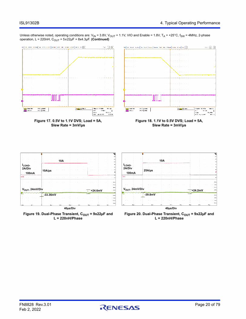
Figure 17. 0.5V to 1.1V DVS; Load = 5A, Slew Rate = 3mV/µs
Figure 18. 1.1V to 0.5V DVS; Load = 5A, Slew Rate = 3mV/µs
Figure 19. Dual-Phase Transient, COUT = 9x22µF and L = 220nH/Phase
Figure 20. Dual-Phase Transient, COUT = 9x22µF and L = 220nH/Phase
Unless otherwise noted, operating conditions are: VIN = 3.8V, VOUT = 1.1V, VIO and Enable = 1.8V, TA = +25°C, fSW = 4MHz, 2-phase operation, L = 220nH, COUT = 5x22µF + 8x4.3µF. (Continued)
10A
10A/µs
ILOAD,2A/Div
100mA
VOUT, 24mV/Div
-33.36mV
+24.6mV
40µs/Div
10A
25A/µs
ILOAD,2A/Div
100mA
VOUT, 24mV/Div
-39.8mV
+24.2mV
40µs/Div
FN8828 Rev.3.01 Page 21 of 79Feb 2, 2022
ISL91302B 5. Applications Information
5. Applications Information
5.1 Inductor SelectionThe ISL91302B is a high efficiency, high performance, dual output multiphase/single-phase synchronous buck converter that can deliver up to 5A of continuous current per phase at 0.3V to 2.0V regulated voltage from a single Li-Ion battery to power portable and handheld devices. The ISL91302B is designed to provide one or two output voltage rails with operational modes setup to 4+0, 3+1, and 2+2 at a nominal switching frequency of 2MHz~4MHz. Contact support for questions relating to switching frequency of 6MHz. Switching MOSFETs are fully integrated and no additional external MOSFETs or diodes are needed. Each phase requires an equal external inductor that can deliver the maximum load current divided by the number of phases used.
5.2 Output Capacitor SelectionOutput capacitors are needed to provide filtering of square voltage at the phase node into a regulated output voltage. The amount of output capacitance required is based on the parameters of the maximum load step, the slew rate of the load step, and the maximum allowable voltage regulation tolerance during the transient. The amount of ripple voltage at the output capacitor is also a design constraint; the total peak-to-peak ripple voltages produced from the output capacitor is equal to its ESR multiplied by the worst case inductor ripple current.
Make sure to select X7R or X5R type capacitors and consider for DC bias effects. A wide range of output capacitor values can be used.
Table 5. Recommended Output Inductors
Manufacturer Part Number L x W x H (mm) Value (nH) DCR mΩ (Typ) ISAT (Typ)
Cyntec HMLB25201T 2.5x2.0x1.0 220 9.4 7.0
Taiyo Yuden MAKK2520HR22M 2.5x2.0x1.0 220 16 8.5
Cyntec HTTN2016T 2.0x1.6x1.0 220 13 7.2
Murata DFE2016E 2.0x1.6x1.0 240 16 7.0
Murata DFE252012F 2.5x2.0x1.2 470 23 6.7
Table 6. Recommended Output Capacitors
Manufacturer Part Number Case Size Value (µF) Voltage Rating (V)
TDK C1608X5R1A226M080AC 0603 22 10
TDK C0510X6S0G105M030AC 0204 1 4
Murata LLD154R60G435ME01 0402 4.3 4
Murata LLL1U4R60G435ME22 0204 4.3 4

FN8828 Rev.3.01 Page 22 of 79Feb 2, 2022
ISL91302B 5. Applications Information
5.3 Input Capacitor SelectionCeramic input capacitors source the AC component of the input current flowing into the high-side MOSFETs. Place them as close to the IC as possible. If long wires are used to bring power to the IC, use additional bulk capacitors between CIN and the battery/power supply to dampen ringing and overshoot at startup.
Internal analog reference circuits also require additional filtering at the AVIN_FLTR pin. A 10µF local decoupling capacitor is recommended for each phase on PVIN.
5.4 ADC TelemetryThe device features a 12-bit (effective) SAR ADC telemetry function that supports internal silicon temperature, individual phase current, total buck output current, output voltage, and input voltage measurements. Two additional channels provide additional internal or external monitoring. Using these channels requires OTP programming from the factory. The ADC is OTP programmed to be turned off during Discontinuous Conduction mode to save current and improve light-load efficiency. The ADC supports two operating modes: Continuous Mode, and Non-continuous (or Single-shot or One-shot) Mode.
The telemetry uses a 16-bit output data format (S13.2). It consists of 1-bit sign and 15-bit data. The two LSB bits represent fractional data (after the decimal point). Reading the ADC output is accomplished by reading the respective MSB (8-bit) and LSB (8-bit). Table 8 shows the registers that hold the ADC data. See “Register Description by Address” on page 42 for more information.
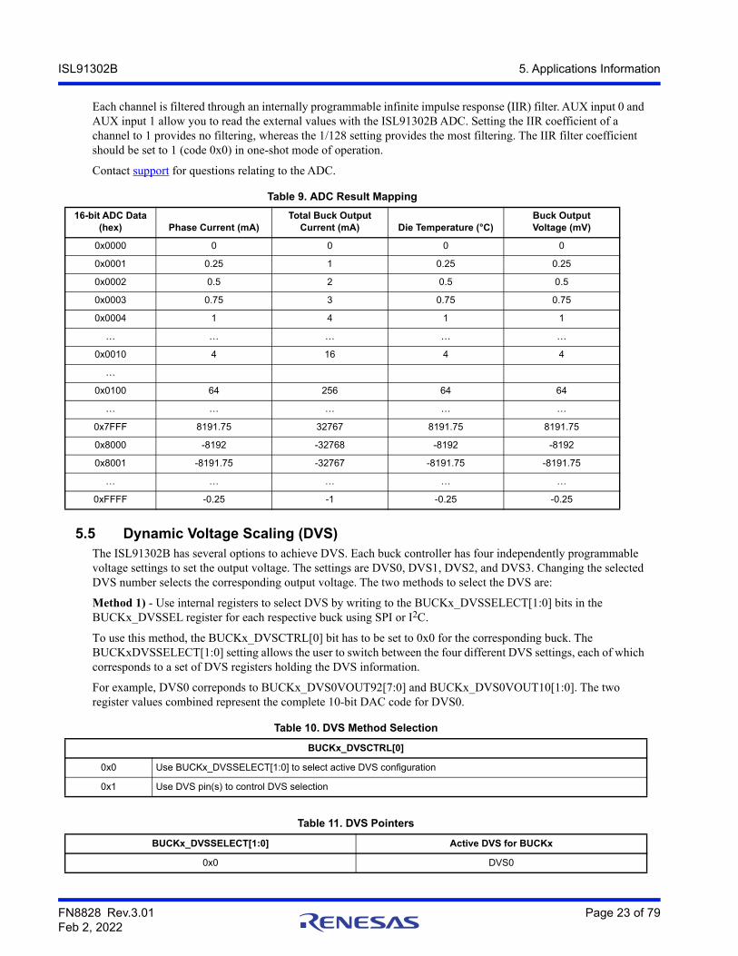
The ADC 16-bit output data LSB is 0.25 when referring to temperature, voltage, or individual phase current. The total buck current measurement has an LSB of 1. See Table 9.
Table 7. Recommended Input Capacitors
Manufacturer Part Number Case Size Value (µF) Volt (V) Input
TDK Corp CGB2A1X5R1A105M033BC 0402 1 10 AVIN
Kemet C0402C104K8RACTU 0402 0.1 10 AVIN
Samsung CL05A10MP5NUNC 0402 10 10 PVIN
Murata GRM188R61A106MAAL 0603 10 10 PVIN
Table 8. ADC Register Addresses
ADC Channel Register NameRegister Address (hex):
ADC MSB DataRegister Address (hex):
ADC LSB Data
Temperature ADC_SAMPLE0MSB/LSB 0x16 0x17
Buck1 Ph1 Current ADC_SAMPLE1PH1MSB/LSB 0x18 0x19
Buck1 Ph2 Current ADC_SAMPLE1PH2MSB/LSB 0x1A 0x1B
Buck1 Ph3 Current ADC_SAMPLE1PH3MSB/LSB 0x1C 0x1D
Buck1 Ph4 Current ADC_SAMPLE1PH4MSB/LSB 0x1E 0x1F
Buck1 Total Current ADC_SAMPLE1TMSB/LSB 0x20 0x21
PVIN for Buck1 ADC_SAMPLE2MSB/LSB 0x22 0x23
VOUT1 ADC_SAMPLE3MSB/LSB 0x24 0x25
Buck2 Ph1 Current ADC_SAMPLE4PH1MSB/LSB 0x26 0x27
Buck2 Ph2 Current ADC_SAMPLE4PH2MSB/LSB 0x28 0x29
Buck2 Total Current ADC_SAMPLE4TMSB/LSB 0x2A 0x2B
PVIN for Buck2 ADC_SAMPLE5MSB/LSB 0x2C 0x2D
VOUT2 ADC_SAMPLE6MSB/LSB 0x2E 0x2F
AUX INPUT0 ADC_AUX0MSB/LSB 0x30 0x31
AUX INPUT1 ADC_AUX1MSB/LSB 0x32 0x33
FN8828 Rev.3.01 Page 23 of 79Feb 2, 2022
ISL91302B 5. Applications Information
Each channel is filtered through an internally programmable infinite impulse response (IIR) filter. AUX input 0 and AUX input 1 allow you to read the external values with the ISL91302B ADC. Setting the IIR coefficient of a channel to 1 provides no filtering, whereas the 1/128 setting provides the most filtering. The IIR filter coefficient should be set to 1 (code 0x0) in one-shot mode of operation.
Contact support for questions relating to the ADC.
5.5 Dynamic Voltage Scaling (DVS) The ISL91302B has several options to achieve DVS. Each buck controller has four independently programmable voltage settings to set the output voltage. The settings are DVS0, DVS1, DVS2, and DVS3. Changing the selected DVS number selects the corresponding output voltage. The two methods to select the DVS are:
Method 1) - Use internal registers to select DVS by writing to the BUCKx_DVSSELECT[1:0] bits in the BUCKx_DVSSEL register for each respective buck using SPI or I2C.
To use this method, the BUCKx_DVSCTRL[0] bit has to be set to 0x0 for the corresponding buck. The BUCKxDVSSELECT[1:0] setting allows the user to switch between the four different DVS settings, each of which corresponds to a set of DVS registers holding the DVS information.
For example, DVS0 correponds to BUCKx_DVS0VOUT92[7:0] and BUCKx_DVS0VOUT10[1:0]. The two register values combined represent the complete 10-bit DAC code for DVS0.
Table 9. ADC Result Mapping
16-bit ADC Data (hex) Phase Current (mA)
Total Buck OutputCurrent (mA) Die Temperature (°C)
Buck OutputVoltage (mV)
0x0000 0 0 0 0
0x0001 0.25 1 0.25 0.25
0x0002 0.5 2 0.5 0.5
0x0003 0.75 3 0.75 0.75
0x0004 1 4 1 1
… … … … …
0x0010 4 16 4 4
…
0x0100 64 256 64 64
… … … … …
0x7FFF 8191.75 32767 8191.75 8191.75
0x8000 -8192 -32768 -8192 -8192
0x8001 -8191.75 -32767 -8191.75 -8191.75
… … … … …
0xFFFF -0.25 -1 -0.25 -0.25
Table 10. DVS Method Selection
BUCKx_DVSCTRL[0]
0x0 Use BUCKx_DVSSELECT[1:0] to select active DVS configuration
0x1 Use DVS pin(s) to control DVS selection
Table 11. DVS Pointers
BUCKx_DVSSELECT[1:0] Active DVS for BUCKx
0x0 DVS0
FN8828 Rev.3.01 Page 24 of 79Feb 2, 2022
ISL91302B 5. Applications Information
Each output voltage is set writing a 10-bit word to DVS Configuration 1 (BUCKx_DVS0CFG1 register) and DVS Configuration 0 (BUCKx_DVS0CFG0 register) in each buck. Configuration 1 holds the eight most significant bits and Configuration 0 holds the last two bits of the 10-bit word. The output voltage does not change until the LSB register has been written.
Equation 1 relates the DVS word and VOUT target.
In the application, the 10-bit DVS word should be set to ensure the buck output voltage target is always 0.3V or above.
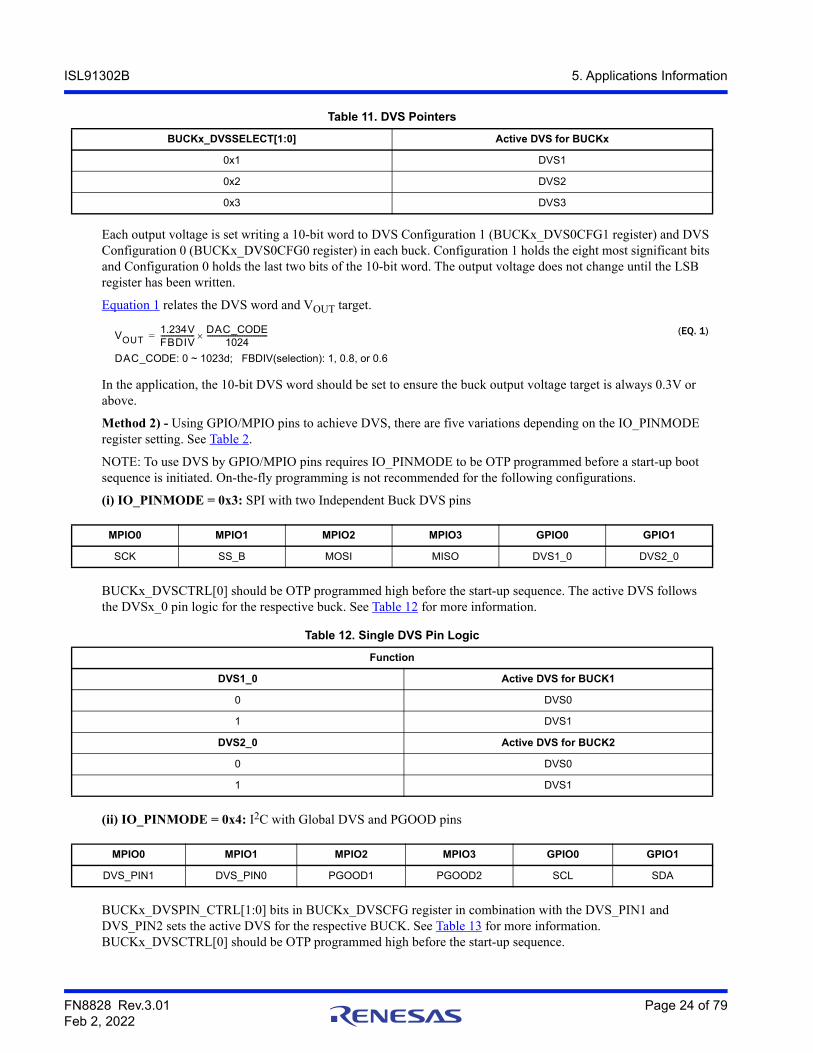
Method 2) - Using GPIO/MPIO pins to achieve DVS, there are five variations depending on the IO_PINMODE register setting. See Table 2.
NOTE: To use DVS by GPIO/MPIO pins requires IO_PINMODE to be OTP programmed before a start-up boot sequence is initiated. On-the-fly programming is not recommended for the following configurations.
(i) IO_PINMODE = 0x3: SPI with two Independent Buck DVS pins
BUCKx_DVSCTRL[0] should be OTP programmed high before the start-up sequence. The active DVS follows the DVSx_0 pin logic for the respective buck. See Table 12 for more information.
(ii) IO_PINMODE = 0x4: I2C with Global DVS and PGOOD pins
BUCKx_DVSPIN_CTRL[1:0] bits in BUCKx_DVSCFG register in combination with the DVS_PIN1 and DVS_PIN2 sets the active DVS for the respective BUCK. See Table 13 for more information. BUCKx_DVSCTRL[0] should be OTP programmed high before the start-up sequence.
0x1 DVS1
0x2 DVS2
0x3 DVS3
MPIO0 MPIO1 MPIO2 MPIO3 GPIO0 GPIO1
SCK SS_B MOSI MISO DVS1_0 DVS2_0
Table 12. Single DVS Pin Logic
Function
DVS1_0 Active DVS for BUCK1
0 DVS0
1 DVS1
DVS2_0 Active DVS for BUCK2
0 DVS0
1 DVS1
MPIO0 MPIO1 MPIO2 MPIO3 GPIO0 GPIO1
DVS_PIN1 DVS_PIN0 PGOOD1 PGOOD2 SCL SDA
Table 11. DVS Pointers
BUCKx_DVSSELECT[1:0] Active DVS for BUCKx
(EQ. 1)VOUT1.234VFBDIV------------------- DAC_CODE
1024----------------------------------=
DAC_CODE: 0 ~ 1023d; FBDIV(selection): 1, 0.8, or 0.6
FN8828 Rev.3.01 Page 25 of 79Feb 2, 2022
ISL91302B 5. Applications Information
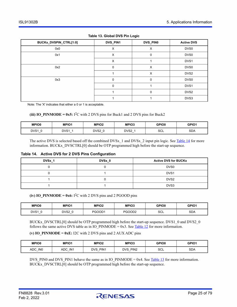
(iii) IO_PINMODE = 0x5: I2C with 2 DVS pins for Buck1 and 2 DVS pins for Buck2
The active DVS is selected based off the combined DVSx_1 and DVSx_2 input pin logic. See Table 14 for more information. BUCKx_DVSCTRL[0] should be OTP programmed high before the start-up sequence.
(iv) IO_PINMODE = 0x6: I2C with 2 DVS pins and 2 PGOOD pins
BUCKx_DVSCTRL[0] should be OTP programmed high before the start-up sequence. DVS1_0 and DVS2_0 follows the same active DVS table as in IO_PINMODE = 0x3. See Table 12 for more information.
(v) IO_PINMODE = 0xE: I2C with 2 DVS pins and 2 AUX ADC pins
DVS_PIN0 and DVS_PIN1 behave the same as in IO_PINMODE = 0x4. See Table 13 for more information. BUCKx_DVSCTRL[0] should be OTP programmed high before the start-up sequence.
Table 13. Global DVS Pin Logic
BUCKx_DVSPIN_CTRL[1:0] DVS_PIN1 DVS_PIN0 Active DVS
0x0 X X DVS0
0x1 X 0 DVS0
X 1 DVS1
0x2 0 X DVS0
1 X DVS2
0x3 0 0 DVS0
0 1 DVS1
1 0 DVS2
1 1 DVS3
Note: The 'X' indicates that either a 0 or 1 is acceptable.
MPIO0 MPIO1 MPIO2 MPIO3 GPIO0 GPIO1
DVS1_0 DVS1_1 DVS2_0 DVS2_1 SCL SDA
Table 14. Active DVS for 2 DVS Pins Configuration
DVSx_1 DVSx_0 Active DVS for BUCKx
0 0 DVS0
0 1 DVS1
1 0 DVS2
1 1 DVS3
MPIO0 MPIO1 MPIO2 MPIO3 GPIO0 GPIO1
DVS1_0 DVS2_0 PGOOD1 PGOOD2 SCL SDA
MPIO0 MPIO1 MPIO2 MPIO3 GPIO0 GPIO1
ADC_IN0 ADC_IN1 DVS_PIN1 DVS_PIN2 SCL SDA
FN8828 Rev.3.01 Page 26 of 79Feb 2, 2022
ISL91302B 5. Applications Information
5.6 Configuring DVS Speed
5.6.1 Power-Up and Shutdown Slew Rate SettingThe BUCKx_RSPPUP[2:0] bits in the BUCKx_RSPCFG0 register set the slew rates (DVS speed) in BUCKx only during VOUTx power-up. Similarly, the BUCKx_RSPPDN[2:0] in the BUCKx_RSPCFG0 register sets the slew rates in BUCKx during normal VOUTx shutdown. The achievable slew rates varies with different FBDIV settings (factory OTP programmed). For more details, see Register BUCK1_RSPCFG0.
5.6.2 DVS Transition Slew Rate SettingBUCKx_RSPUP[2:0] and BUCKx_RSPDN[2:0] in the BUCKx_RSPCFG1 register sets the slew rates (DVS speed) in BUCKx during normal DVS transtion. The achievable slew rates varies with different FBDIV settings (factory OTP programmed). For more details, see Register BUCK1_RSPCFG1.
5.7 Output Voltage SettingEach output voltage is set by writing a 10-bit word to DVS Configuration 1 (BUCKx_DVS0CFG1 register) and DVS Configuration 0 (BUCKx_DVS0CFG0 register) in each buck. Configuration 1 holds the MSB and Configuration 0 holds the last two bits of the 10-bit word. The output voltage does not change until the LSB register has been written. BUCK1_DVS0CFG1 shows the relationship between the DVS word and VOUT.
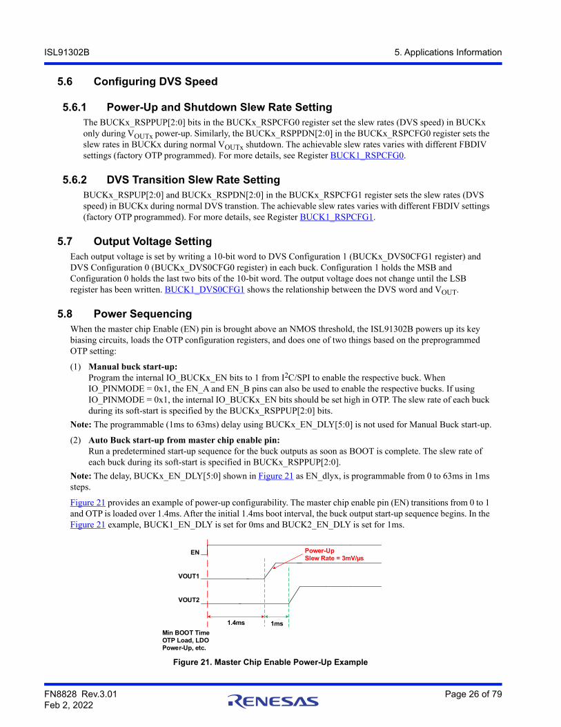
5.8 Power SequencingWhen the master chip Enable (EN) pin is brought above an NMOS threshold, the ISL91302B powers up its key biasing circuits, loads the OTP configuration registers, and does one of two things based on the preprogrammed OTP setting:
(1) Manual buck start-up: Program the internal IO_BUCKx_EN bits to 1 from I2C/SPI to enable the respective buck. When IO_PINMODE = 0x1, the EN_A and EN_B pins can also be used to enable the respective bucks. If using IO_PINMODE = 0x1, the internal IO_BUCKx_EN bits should be set high in OTP. The slew rate of each buck during its soft-start is specified by the BUCKx_RSPPUP[2:0] bits.
Note: The programmable (1ms to 63ms) delay using BUCKx_EN_DLY[5:0] is not used for Manual Buck start-up.
(2) Auto Buck start-up from master chip enable pin: Run a predetermined start-up sequence for the buck outputs as soon as BOOT is complete. The slew rate of each buck during its soft-start is specified in BUCKx_RSPPUP[2:0].
Note: The delay, BUCKx_EN_DLY[5:0] shown in Figure 21 as EN_dlyx, is programmable from 0 to 63ms in 1ms steps.
Figure 21 provides an example of power-up configurability. The master chip enable pin (EN) transitions from 0 to 1 and OTP is loaded over 1.4ms. After the initial 1.4ms boot interval, the buck output start-up sequence begins. In the Figure 21 example, BUCK1_EN_DLY is set for 0ms and BUCK2_EN_DLY is set for 1ms.
Figure 21. Master Chip Enable Power-Up Example
Min BOOT TimeOTP Load, LDO Power-Up, etc.
1.4ms 1ms
Power-UpSlew Rate = 3mV/µs
VOUT1
VOUT2
EN
FN8828 Rev.3.01 Page 27 of 79Feb 2, 2022
ISL91302B 5. Applications Information
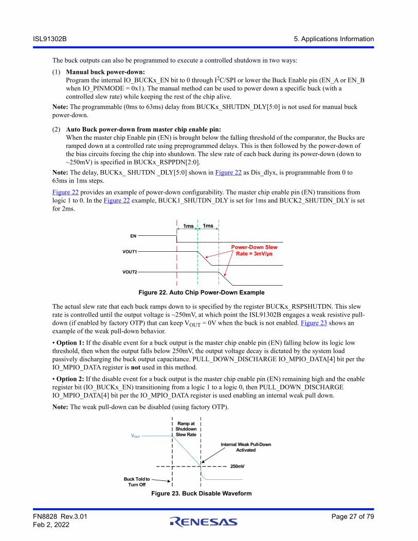
The buck outputs can also be programmed to execute a controlled shutdown in two ways:
(1) Manual buck power-down: Program the internal IO_BUCKx_EN bit to 0 through I2C/SPI or lower the Buck Enable pin (EN_A or EN_B when IO_PINMODE = 0x1). The manual method can be used to power down a specific buck (with a controlled slew rate) while keeping the rest of the chip alive.
Note: The programmable (0ms to 63ms) delay from BUCKx_SHUTDN_DLY[5:0] is not used for manual buck power-down.
(2) Auto Buck power-down from master chip enable pin:When the master chip Enable pin (EN) is brought below the falling threshold of the comparator, the Bucks are ramped down at a controlled rate using preprogrammed delays. This is then followed by the power-down of the bias circuits forcing the chip into shutdown. The slew rate of each buck during its power-down (down to ~250mV) is specified in BUCKx_RSPPDN[2:0].
Note: The delay, BUCKx_ SHUTDN _DLY[5:0] shown in Figure 22 as Dis_dlyx, is programmable from 0 to 63ms in 1ms steps.
Figure 22 provides an example of power-down configurability. The master chip enable pin (EN) transitions from logic 1 to 0. In the Figure 22 example, BUCK1_SHUTDN_DLY is set for 1ms and BUCK2_SHUTDN_DLY is set for 2ms.
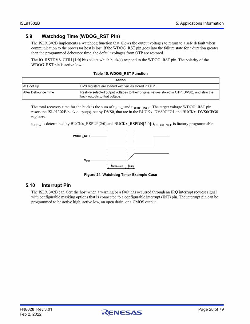
The actual slew rate that each buck ramps down to is specified by the register BUCKx_RSPSHUTDN. This slew rate is controlled until the output voltage is ~250mV, at which point the ISL91302B engages a weak resistive pull-down (if enabled by factory OTP) that can keep VOUT = 0V when the buck is not enabled. Figure 23 shows an example of the weak pull-down behavior.
• Option 1: If the disable event for a buck output is the master chip enable pin (EN) falling below its logic low threshold, then when the output falls below 250mV, the output voltage decay is dictated by the system load passively discharging the buck output capacitance. PULL_DOWN_DISCHARGE IO_MPIO_DATA[4] bit per the IO_MPIO_DATA register is not used in this method.
• Option 2: If the disable event for a buck output is the master chip enable pin (EN) remaining high and the enable register bit (IO_BUCKx_EN) transitioning from a logic 1 to a logic 0, then PULL_DOWN_DISCHARGE IO_MPIO_DATA[4] bit per the IO_MPIO_DATA register is used enabling an internal weak pull down.
Note: The weak pull-down can be disabled (using factory OTP).
Figure 22. Auto Chip Power-Down Example
Figure 23. Buck Disable Waveform
VOUT1
VOUT2
EN
Power-Down SlewRate = 3mV/µs
1ms 1ms
Buck Told toTurn Off
VOUT
Ramp at Shutdown Slew Rate
250mV
Internal Weak Pull-Down Activated
FN8828 Rev.3.01 Page 28 of 79Feb 2, 2022
ISL91302B 5. Applications Information
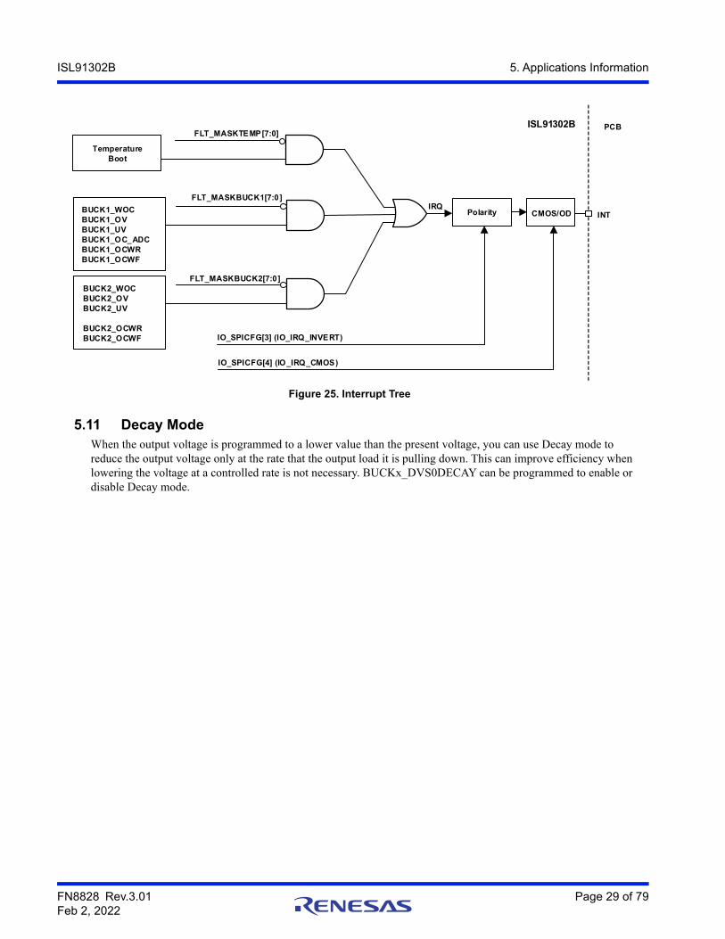
5.9 Watchdog Time (WDOG_RST Pin)The ISL91302B implements a watchdog function that allows the output voltages to return to a safe default when communication to the processor host is lost. If the WDOG_RST pin goes into the failure state for a duration greater than the programmed debounce time, the default voltages from OTP are restored.
The IO_RSTDVS_CTRL[1:0] bits select which buck(s) respond to the WDOG_RST pin. The polarity of the WDOG_RST pin is active low.
The total recovery time for the buck is the sum of tSLEW and tDEBOUNCE. The target voltage WDOG_RST pin resets the ISL91302B buck output(s), set by DVS0, that are in the BUCKx_DVS0CFG1 and BUCKx_DVS0CFG0 registers.
tSLEW is determined by BUCKx_RSPUP[2:0] and BUCKx_RSPDN[2:0]. tDEBOUNCE is factory programmable.
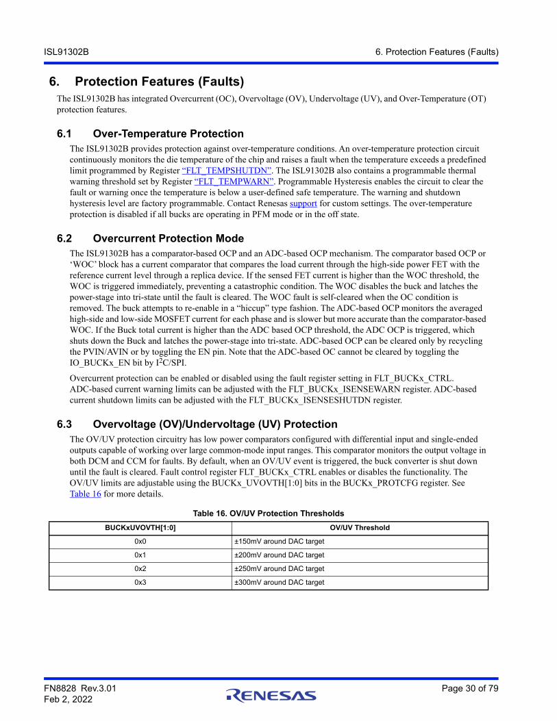
5.10 Interrupt PinThe ISL91302B can alert the host when a warning or a fault has occurred through an IRQ interrupt request signal with configurable masking options that is connected to a configurable interrupt (INT) pin. The interrupt pin can be programmed to be active high, active low, an open drain, or a CMOS output.
Table 15. WDOG_RST Function
Action
At Boot Up DVS registers are loaded with values stored in OTP.
After Debounce Time Restore selected output voltages to their original values stored in OTP (DVS0), and slew the buck outputs to that voltage.
Figure 24. Watchdog Timer Example Case
tDEBOUNCE tSLEW
WDOG_RST
VOUT
FN8828 Rev.3.01 Page 29 of 79Feb 2, 2022
ISL91302B 5. Applications Information
5.11 Decay ModeWhen the output voltage is programmed to a lower value than the present voltage, you can use Decay mode to reduce the output voltage only at the rate that the output load it is pulling down. This can improve efficiency when lowering the voltage at a controlled rate is not necessary. BUCKx_DVS0DECAY can be programmed to enable or disable Decay mode.
Figure 25. Interrupt Tree
FLT_MASKTEMP[7:0]
FLT_MASKBUCK1[7:0]
FLT_MASKBUCK2[7:0]
TemperatureBoot
INT
BUCK2_WOCBUCK2_OVBUCK2_UV
BUCK2_OCWRBUCK2_OCWF
BUCK1_WOCBUCK1_OVBUCK1_UVBUCK1_OC_ADCBUCK1_OCWRBUCK1_OCWF
ISL91302B PCB
IRQ
IO_SPICFG[4] (IO_IRQ_CMOS)
IO_SPICFG[3] (IO_IRQ_INVERT)
CMOS/OD Polarity
FN8828 Rev.3.01 Page 30 of 79Feb 2, 2022
ISL91302B 6. Protection Features (Faults)
6. Protection Features (Faults)The ISL91302B has integrated Overcurrent (OC), Overvoltage (OV), Undervoltage (UV), and Over-Temperature (OT) protection features.
6.1 Over-Temperature ProtectionThe ISL91302B provides protection against over-temperature conditions. An over-temperature protection circuit continuously monitors the die temperature of the chip and raises a fault when the temperature exceeds a predefined limit programmed by Register “FLT_TEMPSHUTDN”. The ISL91302B also contains a programmable thermal warning threshold set by Register “FLT_TEMPWARN”. Programmable Hysteresis enables the circuit to clear the fault or warning once the temperature is below a user-defined safe temperature. The warning and shutdown hysteresis level are factory programmable. Contact Renesas support for custom settings. The over-temperature protection is disabled if all bucks are operating in PFM mode or in the off state.
6.2 Overcurrent Protection ModeThe ISL91302B has a comparator-based OCP and an ADC-based OCP mechanism. The comparator based OCP or ‘WOC’ block has a current comparator that compares the load current through the high-side power FET with the reference current level through a replica device. If the sensed FET current is higher than the WOC threshold, the WOC is triggered immediately, preventing a catastrophic condition. The WOC disables the buck and latches the power-stage into tri-state until the fault is cleared. The WOC fault is self-cleared when the OC condition is removed. The buck attempts to re-enable in a “hiccup” type fashion. The ADC-based OCP monitors the averaged high-side and low-side MOSFET current for each phase and is slower but more accurate than the comparator-based WOC. If the Buck total current is higher than the ADC based OCP threshold, the ADC OCP is triggered, which shuts down the Buck and latches the power-stage into tri-state. ADC-based OCP can be cleared only by recycling the PVIN/AVIN or by toggling the EN pin. Note that the ADC-based OC cannot be cleared by toggling the IO_BUCKx_EN bit by I2C/SPI.
Overcurrent protection can be enabled or disabled using the fault register setting in FLT_BUCKx_CTRL. ADC-based current warning limits can be adjusted with the FLT_BUCKx_ISENSEWARN register. ADC-based current shutdown limits can be adjusted with the FLT_BUCKx_ISENSESHUTDN register.
6.3 Overvoltage (OV)/Undervoltage (UV) ProtectionThe OV/UV protection circuitry has low power comparators configured with differential input and single-ended outputs capable of working over large common-mode input ranges. This comparator monitors the output voltage in both DCM and CCM for faults. By default, when an OV/UV event is triggered, the buck converter is shut down until the fault is cleared. Fault control register FLT_BUCKx_CTRL enables or disables the functionality. The OV/UV limits are adjustable using the BUCKx_UVOVTH[1:0] bits in the BUCKx_PROTCFG register. See Table 16 for more details.
Table 16. OV/UV Protection Thresholds
BUCKxUVOVTH[1:0] OV/UV Threshold
0x0 ±150mV around DAC target
0x1 ±200mV around DAC target
0x2 ±250mV around DAC target
0x3 ±300mV around DAC target

FN8828 Rev.3.01 Page 31 of 79Feb 2, 2022
ISL91302B 7. Serial Communication Interface
7. Serial Communication InterfaceThe ISL91302B has two serial interface protocols to read/write the registers.
• SPI
• I2C
The arbitration of the register access bus between SPI and I2C is determined by the pad MPIO1 when using IO_PINMODE = 0x0, as shown in Table 17:
After switching from SPI to I2C or vice versa, a minimum of 50ns wait time is required before starting a transaction.
7.1 SPI Serial InterfaceThe SPI interface is a general specification 4-wire slave interface capable of operating at a clock speed of up to 26MHz. It is based on byte transfers. The ISL91302B does not support SPI reads on the MISO bus when using multiple slave devices on the same bus.
7.1.1 SPI Data ProtocolBoth Read and Write SPI transactions begin when SS_B goes low and end when SS_B goes high.
7.1.1.1 Write Operation To write to the ISL91302B, the master (controller) needs to drive SS_B low, then send the Control Byte followed by the register address, packet length (if IO_SPIMODE = 1), and data bytes to be written. The controller drives SS_B high to terminate the transaction as shown in Figure 27.
Figure 26. SPI and I2C Interface Block Diagram
Table 17. SPI/I2C Register Access
RegisterIO_PINMODE
PadMPIO_1 (SS_B) Register Access
0 0 SPI (read/write access (Note 11))
1 I2C (Note 12)
Notes:11. When the device is configured for SPI access, the I2C should not be addressed with the device ID.12. When the device is configured for I2C access in PINMODE 0, the SS_B line must be held high.
MPIO3
MPIO2
MPIO1
MPIO0
I2C-IO
I2C-IO
SPIController
I2CController
Registers
OTP
PINMODE
MISO
MOSI
SS_B
SCK
VIO
SDA
SCL
FN8828 Rev.3.01 Page 32 of 79Feb 2, 2022
ISL91302B 7. Serial Communication Interface
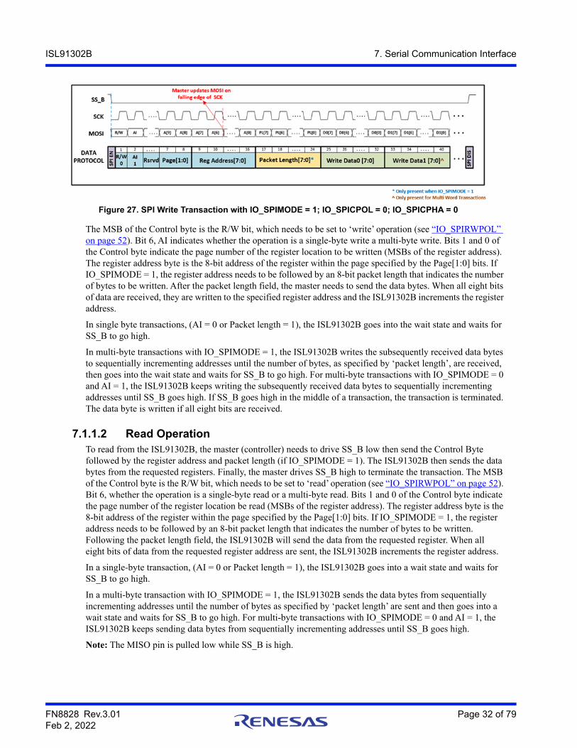
The MSB of the Control byte is the R/W bit, which needs to be set to ‘write’ operation (see “IO_SPIRWPOL” on page 52). Bit 6, AI indicates whether the operation is a single-byte write a multi-byte write. Bits 1 and 0 of the Control byte indicate the page number of the register location to be written (MSBs of the register address). The register address byte is the 8-bit address of the register within the page specified by the Page[1:0] bits. If IO_SPIMODE = 1, the register address needs to be followed by an 8-bit packet length that indicates the number of bytes to be written. After the packet length field, the master needs to send the data bytes. When all eight bits of data are received, they are written to the specified register address and the ISL91302B increments the register address.
In single byte transactions, (AI = 0 or Packet length = 1), the ISL91302B goes into the wait state and waits for SS_B to go high.
In multi-byte transactions with IO_SPIMODE = 1, the ISL91302B writes the subsequently received data bytes to sequentially incrementing addresses until the number of bytes, as specified by ‘packet length’, are received, then goes into the wait state and waits for SS_B to go high. For multi-byte transactions with IO_SPIMODE = 0 and AI = 1, the ISL91302B keeps writing the subsequently received data bytes to sequentially incrementing addresses until SS_B goes high. If SS_B goes high in the middle of a transaction, the transaction is terminated. The data byte is written if all eight bits are received.
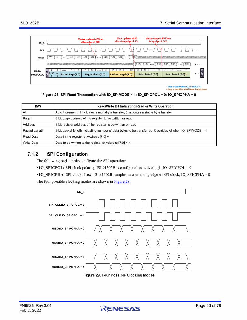
7.1.1.2 Read Operation To read from the ISL91302B, the master (controller) needs to drive SS_B low then send the Control Byte followed by the register address and packet length (if IO_SPIMODE = 1). The ISL91302B then sends the data bytes from the requested registers. Finally, the master drives SS_B high to terminate the transaction. The MSB of the Control byte is the R/W bit, which needs to be set to ‘read’ operation (see “IO_SPIRWPOL” on page 52). Bit 6, whether the operation is a single-byte read or a multi-byte read. Bits 1 and 0 of the Control byte indicate the page number of the register location be read (MSBs of the register address). The register address byte is the 8-bit address of the register within the page specified by the Page[1:0] bits. If IO_SPIMODE = 1, the register address needs to be followed by an 8-bit packet length that indicates the number of bytes to be written. Following the packet length field, the ISL91302B will send the data from the requested register. When all eight bits of data from the requested register address are sent, the ISL91302B increments the register address.
In a single-byte transaction, (AI = 0 or Packet length = 1), the ISL91302B goes into a wait state and waits for SS_B to go high.
In a multi-byte transaction with IO_SPIMODE = 1, the ISL91302B sends the data bytes from sequentially incrementing addresses until the number of bytes as specified by ‘packet length’ are sent and then goes into a wait state and waits for SS_B to go high. For multi-byte transactions with IO_SPIMODE = 0 and AI = 1, the ISL91302B keeps sending data bytes from sequentially incrementing addresses until SS_B goes high.
Note: The MISO pin is pulled low while SS_B is high.
Figure 27. SPI Write Transaction with IO_SPIMODE = 1; IO_SPICPOL = 0; IO_SPICPHA = 0
FN8828 Rev.3.01 Page 33 of 79Feb 2, 2022
ISL91302B 7. Serial Communication Interface
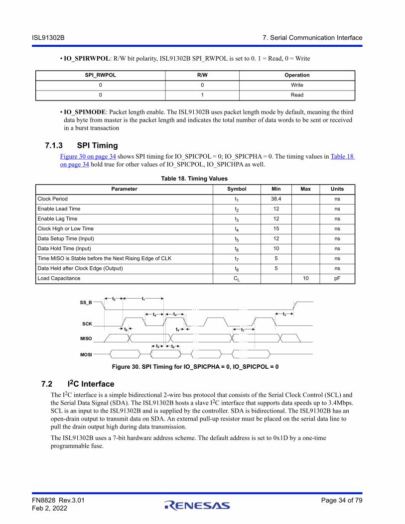
7.1.2 SPI ConfigurationThe following register bits configure the SPI operation:
• IO_SPICPOL: SPI clock polarity, ISL91302B is configured as active high, IO_SPICPOL = 0
• IO_SPICPHA: SPI clock phase, ISL91302B samples data on rising edge of SPI clock, IO_SPICPHA = 0
The four possible clocking modes are shown in Figure 29.
Figure 28. SPI Read Transaction with IO_SPIMODE = 1; IO_SPICPOL = 0; IO_SPICPHA = 0
R/W Read/Write Bit Indicating Read or Write Operation
AI Auto Increment. 1 indicates a multi-byte transfer, 0 indicates a single byte transfer
Page 2-bit page address of the register to be written or read
Address 8-bit register address of the register to be written or read
Packet Length 8-bit packet length indicating number of data bytes to be transferred. Overrides AI when IO_SPIMODE = 1
Read Data Data in the register at Address [7:0] + n
Write Data Data to be written to the register at Address [7:0] + n
Figure 29. Four Possible Clocking Modes
SS_B
SPI_CLK:IO_SPICPOL = 0
SPI_CLK:IO_SPICPOL = 1
MISO:IO_SPIPCPHA = 0
MOSI:IO_SPIPCPHA = 0
MISO:IO_SPIPCPHA = 1
MOSI:IO_SPIPCPHA = 1
FN8828 Rev.3.01 Page 34 of 79Feb 2, 2022
ISL91302B 7. Serial Communication Interface
• IO_SPIRWPOL: R/W bit polarity, ISL91302B SPI_RWPOL is set to 0. 1 = Read, 0 = Write
• IO_SPIMODE: Packet length enable. The ISL91302B uses packet length mode by default, meaning the third data byte from master is the packet length and indicates the total number of data words to be sent or received in a burst transaction
7.1.3 SPI TimingFigure 30 on page 34 shows SPI timing for IO_SPICPOL = 0; IO_SPICPHA = 0. The timing values in Table 18 on page 34 hold true for other values of IO_SPICPOL, IO_SPICHPA as well.
7.2 I2C InterfaceThe I2C interface is a simple bidirectional 2-wire bus protocol that consists of the Serial Clock Control (SCL) and the Serial Data Signal (SDA). The ISL91302B hosts a slave I2C interface that supports data speeds up to 3.4Mbps. SCL is an input to the ISL91302B and is supplied by the controller. SDA is bidirectional. The ISL91302B has an open-drain output to transmit data on SDA. An external pull-up resistor must be placed on the serial data line to pull the drain output high during data transmission.
The ISL91302B uses a 7-bit hardware address scheme. The default address is set to 0x1D by a one-time programmable fuse.
SPI_RWPOL R/W Operation
0 0 Write
0 1 Read
Table 18. Timing Values
Parameter Symbol Min Max Units
Clock Period t1 38.4 ns
Enable Lead Time t2 12 ns
Enable Lag Time t3 12 ns
Clock High or Low Time t4 15 ns
Data Setup Time (Input) t5 12 ns
Data Hold Time (Input) t6 10 ns
Time MISO is Stable before the Next Rising Edge of CLK t7 5 ns
Data Held after Clock Edge (Output) t8 5 ns
Load Capacitance CL 10 pF
Figure 30. SPI Timing for IO_SPICPHA = 0, IO_SPICPOL = 0
MISO
SCK
SS_B
MOSI```
t2 t1
t4 t4
t8 t9
t5 t6
t7
t3
FN8828 Rev.3.01 Page 35 of 79Feb 2, 2022
ISL91302B 7. Serial Communication Interface
7.2.1 I2C Bus OperationThe chip supports 7-bit addressing. The ISL91302B I2C device address is reconfigurable through the OTP.
All communication over the I2C interface is conducted by sending the MSB of each byte of data first. Data states on the SDA line can change only during SCL LOW periods. SDA state changes during SCL HIGH are reserved for indicating START and STOP conditions (see Figure 35 on page 36).
All I2C interface operations must begin with a START condition, which is a HIGH to LOW transition of SDA while SCL is HIGH. The ISL91302B continuously monitors the SDA and SCL lines for the START condition and does not respond to any command until this condition is met. All I2C interface operations must be terminated by a STOP condition, which is a LOW to HIGH transition of SDA while SCL is HIGH.
An Acknowledge (or ACK), is a software convention that indicates a successful data transfer. The transmitting device, either master or slave, releases the SDA bus after transmitting eight bits. During the ninth clock cycle, the receiver pulls the SDA line LOW to acknowledge the reception of the eight bits of data (Figure 35 on page 36). The ISL91302B responds with an ACK after recognizing a START condition, followed by a valid Identification Byte (also known as I2C Address). The ISL91302B also responds with an ACK after receiving a Data Byte of a write operation. The master must respond with an ACK after receiving a Data Byte of a read operation.
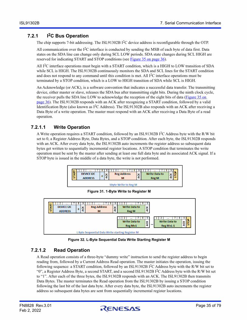
7.2.1.1 Write Operation A Write operation requires a START condition, followed by an ISL91302B I2C Address byte with the R/W bit set to 0, a Register Address Byte, Data Bytes, and a STOP condition. After each byte, the ISL91302B responds with an ACK. After every data byte, the ISL91302B auto increments the register address so subsequent data bytes get written to sequentially incremental register locations. A STOP condition that terminates the write operation must be sent by the master after sending at least one full data byte and its associated ACK signal. If a STOP byte is issued in the middle of a data byte, the write is not performed.
Figure 31. 1-Byte Write to Register M
Figure 32. L-Byte Sequential Data Write Starting Register M
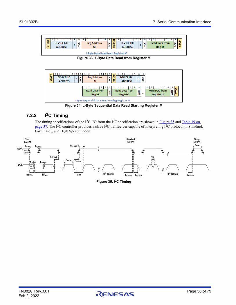
7.2.1.2 Read Operation A Read operation consists of a three-byte “dummy write” instruction to send the register address to begin reading from, followed by a Current Address Read operation. The master initiates the operation, issuing the following sequence: a START condition, followed by an ISL91302B I2C Address byte with the R/W bit set to “0”, a Register Address Byte, a second START, and a second ISL91302B I2C Address byte with the R/W bit set to “1”. After each of the three bytes, the ISL91302B responds with an ACK. The ISL91302B then transmits Data Bytes. The master terminates the Read operation from the ISL91302B by issuing a STOP condition following the last bit of the last data byte. After every data byte, the ISL91302B auto increments the register address so subsequent data bytes are sent from sequentially incremental register locations.
FN8828 Rev.3.01 Page 36 of 79Feb 2, 2022
ISL91302B 7. Serial Communication Interface
Figure 33. 1-Byte Data Read from Register M
Figure 34. L-Byte Sequential Data Read Starting Register M
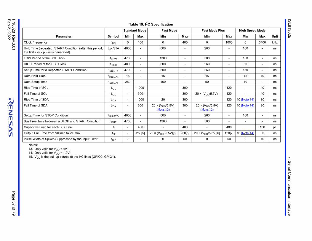
7.2.2 I2C Timing The timing specifications of the I2C I/O from the I2C specification are shown in Figure 35 and Table 19 on page 37. The I2C controller provides a slave I2C transceiver capable of interpreting I2C protocol in Standard, Fast, Fast+, and High Speed modes.
Figure 35. I2C Timing
70%30%
SDAtf
tf
Start Event
tHD:STA 1/fSCL
tr
tr
tHD:DAT
tSU:DAT
tLOW
tHIGH tVD:DAT
9th Clock
Restart Event
tHD:STAtSU:STA
tSP
9th Clock
tBUF
tSU:STA
Stop Event
SCL70%30%
FN
882
8R
ev.3
.01
Pa
ge 3
7 of 79
Feb
2, 20
22
ISL
913
02B
7. S
erial Co
mm
unication
Inte
rfaceTable 19. I2C Specification
Parameter Symbol
Standard Mode Fast Mode Fast Mode Plus High Speed Mode
UnitMin Max Min Max Min Max Min Max
Clock Frequency fSCL 0 100 0 400 0 1000 0 3400 kHz
Hold Time (repeated) START Condition (after this period, the first clock pulse is generated)
tHD;STA 4000 - 600 - 260 - 160 - ns
LOW Period of the SCL Clock tLOW 4700 - 1300 - 500 - 160 - ns
HIGH Period of the SCL Clock tHIGH 4000 - 600 - 260 - 60 - ns
Setup Time for a Repeated START Condition tSU;STA 4700 - 600 - 260 - 160 - ns
Data Hold Time tHD;DAT 15 - 15 - 15 - 15 70 ns
Data Setup Time tSU;DAT 250 - 100 - 50 - 10 - ns
Rise Time of SCL trCL - 1000 - 300 - 120 - 40 ns
Fall Time of SCL tfCL - 300 - 300 20 × (VDD/5.5V)- 120 - 40 ns
Rise Time of SDA trDA - 1000 20 300 - 120 10 (Note 14) 80 ns
Fall Time of SDA tfDA - 300 20 × (VDD/5.5V) (Note 13)
300 20 × (VDD/5.5V) (Note 13)
120 10 (Note 14) 80 ns
Setup Time for STOP Condition tSU;STO 4000 - 600 - 260 - 160 - ns
Bus Free Time between a STOP and START Condition tBUF 4700 - 1300 - 500 - - - ns
Capacitive Load for each Bus Line Cb - 400 - 400 - 400 100 pF
Output Fall Time from VIHmin to VILmax tof - 250[5] 20 × (VDD /5.5V)[6] 250[5] 20 × (VDD/5.5V)[6] 120[7] 10 (Note 14) 80 ns
Pulse Width of Spikes Suppressed by the Input Filter tSP - - 0 50 0 50 0 10 ns
Notes:13. Only valid for VDD < 4V.14. Only valid for VDD < 1.9V.15. VDD is the pull-up source to the I2C lines (GPIO0, GPIO1).
FN8828 Rev.3.01 Page 38 of 79Feb 2, 2022
ISL91302B 8. Board Layout Recommendations
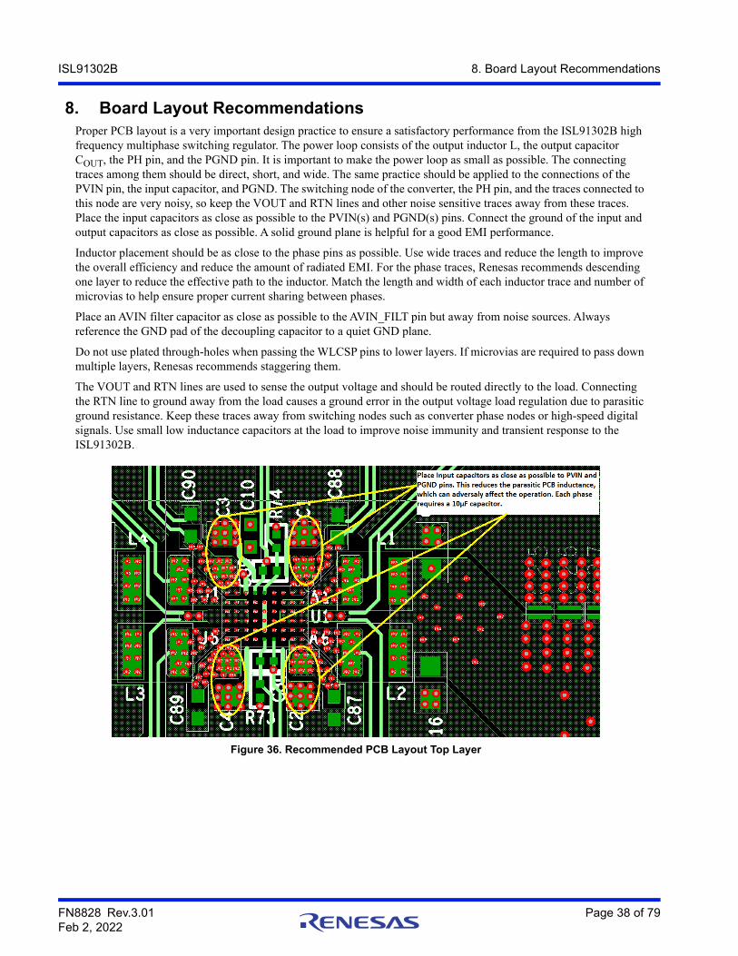
8. Board Layout RecommendationsProper PCB layout is a very important design practice to ensure a satisfactory performance from the ISL91302B high frequency multiphase switching regulator. The power loop consists of the output inductor L, the output capacitor COUT, the PH pin, and the PGND pin. It is important to make the power loop as small as possible. The connecting traces among them should be direct, short, and wide. The same practice should be applied to the connections of the PVIN pin, the input capacitor, and PGND. The switching node of the converter, the PH pin, and the traces connected to this node are very noisy, so keep the VOUT and RTN lines and other noise sensitive traces away from these traces. Place the input capacitors as close as possible to the PVIN(s) and PGND(s) pins. Connect the ground of the input and output capacitors as close as possible. A solid ground plane is helpful for a good EMI performance.
Inductor placement should be as close to the phase pins as possible. Use wide traces and reduce the length to improve the overall efficiency and reduce the amount of radiated EMI. For the phase traces, Renesas recommends descending one layer to reduce the effective path to the inductor. Match the length and width of each inductor trace and number of microvias to help ensure proper current sharing between phases.
Place an AVIN filter capacitor as close as possible to the AVIN_FILT pin but away from noise sources. Always reference the GND pad of the decoupling capacitor to a quiet GND plane.
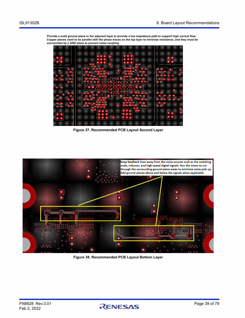
Do not use plated through-holes when passing the WLCSP pins to lower layers. If microvias are required to pass down multiple layers, Renesas recommends staggering them.
The VOUT and RTN lines are used to sense the output voltage and should be routed directly to the load. Connecting the RTN line to ground away from the load causes a ground error in the output voltage load regulation due to parasitic ground resistance. Keep these traces away from switching nodes such as converter phase nodes or high-speed digital signals. Use small low inductance capacitors at the load to improve noise immunity and transient response to the ISL91302B.
Figure 36. Recommended PCB Layout Top Layer
FN8828 Rev.3.01 Page 39 of 79Feb 2, 2022
ISL91302B 8. Board Layout Recommendations
Figure 37. Recommended PCB Layout Second Layer
Figure 38. Recommended PCB Layout Bottom Layer
Provide a solid ground plane in the adjacent layer to provide a low impedance path to support high current flow.Copper planes need to be parallel with the phase traces on the top layer to minimize resistance, and they must besurrounded by a GND plane to prevent noise coupling.
FN8828 Rev.3.01 Page 40 of 79Feb 2, 2022
ISL91302B 8. Board Layout Recommendations
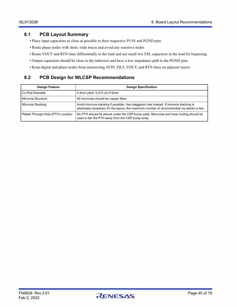
8.1 PCB Layout Summary• Place input capacitors as close as possible to their respective PVIN and PGND pins
• Route phase nodes with short, wide traces and avoid any sensitive nodes
• Route VOUT and RTN lines differentially to the load and use small low ESL capacitors at the load for bypassing
• Output capacitors should be close to the inductors and have a low impedance path to the PGND pins
• Keep digital and phase nodes from intersecting AVIN_FILT, VOUT, and RTN lines on adjacent layers
8.2 PCB Design for WLCSP Recommendations
Design Feature Design Specification
Cu Pad Diameter 0.4mm pitch: 0.215 ±0.012mm
Microvia Structure All microvias should be copper filled.
Microvia Stacking Avoid microvia stacking if possible. Use staggered vias instead. If microvia stacking is absolutely necessary for the layout, the maximum number of recommended via stacks is two.
Plated Through-Hole (PTH) Location No PTH should be placed under the CSP bump pads. Microvias and trace routing should be used to fan the PTH away from the CSP bump array.
FN8828 Rev.3.01 Page 41 of 79Feb 2, 2022
ISL91302B 9. Register Address Map
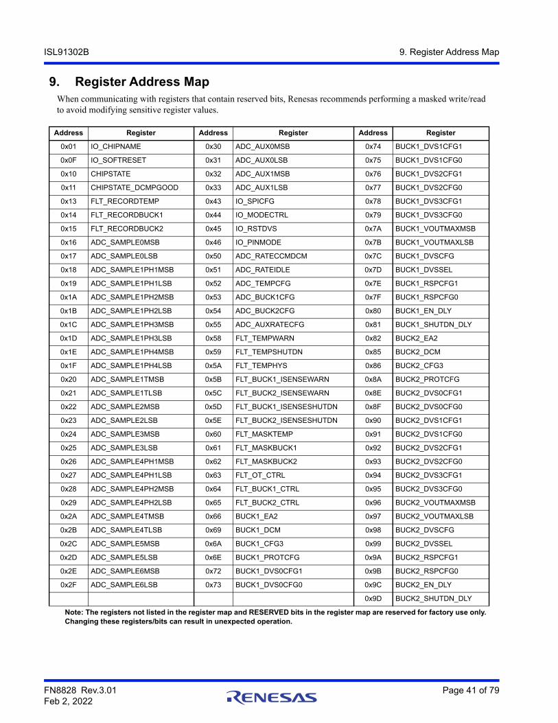
9. Register Address MapWhen communicating with registers that contain reserved bits, Renesas recommends performing a masked write/read to avoid modifying sensitive register values.
Address Register Address Register Address Register
0x01 IO_CHIPNAME 0x30 ADC_AUX0MSB 0x74 BUCK1_DVS1CFG1
0x0F IO_SOFTRESET 0x31 ADC_AUX0LSB 0x75 BUCK1_DVS1CFG0
0x10 CHIPSTATE 0x32 ADC_AUX1MSB 0x76 BUCK1_DVS2CFG1
0x11 CHIPSTATE_DCMPGOOD 0x33 ADC_AUX1LSB 0x77 BUCK1_DVS2CFG0
0x13 FLT_RECORDTEMP 0x43 IO_SPICFG 0x78 BUCK1_DVS3CFG1
0x14 FLT_RECORDBUCK1 0x44 IO_MODECTRL 0x79 BUCK1_DVS3CFG0
0x15 FLT_RECORDBUCK2 0x45 IO_RSTDVS 0x7A BUCK1_VOUTMAXMSB
0x16 ADC_SAMPLE0MSB 0x46 IO_PINMODE 0x7B BUCK1_VOUTMAXLSB
0x17 ADC_SAMPLE0LSB 0x50 ADC_RATECCMDCM 0x7C BUCK1_DVSCFG
0x18 ADC_SAMPLE1PH1MSB 0x51 ADC_RATEIDLE 0x7D BUCK1_DVSSEL
0x19 ADC_SAMPLE1PH1LSB 0x52 ADC_TEMPCFG 0x7E BUCK1_RSPCFG1
0x1A ADC_SAMPLE1PH2MSB 0x53 ADC_BUCK1CFG 0x7F BUCK1_RSPCFG0
0x1B ADC_SAMPLE1PH2LSB 0x54 ADC_BUCK2CFG 0x80 BUCK1_EN_DLY
0x1C ADC_SAMPLE1PH3MSB 0x55 ADC_AUXRATECFG 0x81 BUCK1_SHUTDN_DLY
0x1D ADC_SAMPLE1PH3LSB 0x58 FLT_TEMPWARN 0x82 BUCK2_EA2
0x1E ADC_SAMPLE1PH4MSB 0x59 FLT_TEMPSHUTDN 0x85 BUCK2_DCM
0x1F ADC_SAMPLE1PH4LSB 0x5A FLT_TEMPHYS 0x86 BUCK2_CFG3
0x20 ADC_SAMPLE1TMSB 0x5B FLT_BUCK1_ISENSEWARN 0x8A BUCK2_PROTCFG
0x21 ADC_SAMPLE1TLSB 0x5C FLT_BUCK2_ISENSEWARN 0x8E BUCK2_DVS0CFG1
0x22 ADC_SAMPLE2MSB 0x5D FLT_BUCK1_ISENSESHUTDN 0x8F BUCK2_DVS0CFG0
0x23 ADC_SAMPLE2LSB 0x5E FLT_BUCK2_ISENSESHUTDN 0x90 BUCK2_DVS1CFG1
0x24 ADC_SAMPLE3MSB 0x60 FLT_MASKTEMP 0x91 BUCK2_DVS1CFG0
0x25 ADC_SAMPLE3LSB 0x61 FLT_MASKBUCK1 0x92 BUCK2_DVS2CFG1
0x26 ADC_SAMPLE4PH1MSB 0x62 FLT_MASKBUCK2 0x93 BUCK2_DVS2CFG0
0x27 ADC_SAMPLE4PH1LSB 0x63 FLT_OT_CTRL 0x94 BUCK2_DVS3CFG1
0x28 ADC_SAMPLE4PH2MSB 0x64 FLT_BUCK1_CTRL 0x95 BUCK2_DVS3CFG0
0x29 ADC_SAMPLE4PH2LSB 0x65 FLT_BUCK2_CTRL 0x96 BUCK2_VOUTMAXMSB
0x2A ADC_SAMPLE4TMSB 0x66 BUCK1_EA2 0x97 BUCK2_VOUTMAXLSB
0x2B ADC_SAMPLE4TLSB 0x69 BUCK1_DCM 0x98 BUCK2_DVSCFG
0x2C ADC_SAMPLE5MSB 0x6A BUCK1_CFG3 0x99 BUCK2_DVSSEL
0x2D ADC_SAMPLE5LSB 0x6E BUCK1_PROTCFG 0x9A BUCK2_RSPCFG1
0x2E ADC_SAMPLE6MSB 0x72 BUCK1_DVS0CFG1 0x9B BUCK2_RSPCFG0
0x2F ADC_SAMPLE6LSB 0x73 BUCK1_DVS0CFG0 0x9C BUCK2_EN_DLY
0x9D BUCK2_SHUTDN_DLY
Note: The registers not listed in the register map and RESERVED bits in the register map are reserved for factory use only.Changing these registers/bits can result in unexpected operation.
FN8828 Rev.3.01 Page 42 of 79Feb 2, 2022
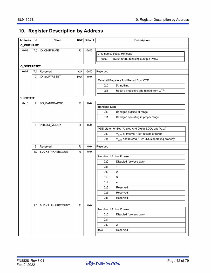
ISL91302B 10. Register Description by Address
10. Register Description by Address
Address Bit Name R/W Default Description
IO_CHIPNAME
0x01 7:0 IO_CHIPNAME R 0x02
IO_SOFTRESET
0x0F 7:1 Reserved N/A 0x00 Reserved
0 IO_SOFTRESET R/W 0x0
CHIPSTATE
0x10 7 BG_BANDGAPOK R 0x0
6 INTLDO_VDDOK R 0x0
5 Reserved R 0x0 Reserved
4:2 BUCK1_PHASECOUNT R 0x0
1:0 BUCK2_PHASECOUNT R 0x0
Chip name. Set by Renesas
0x02 ISL91302B, dual/single output PMIC
Reset all Registers And Reload from OTP
0x0 Do nothing
0x1 Reset all registers and reload from OTP
Bandgap State
0x0 Bandgap outside of range
0x1 Bandgap operating in proper range
VDD state (for Both Analog And Digital LDOs and VBAT)
0x0 VBAT or Internal 1.5V outside of range
0x1 VBAT and Internal 1.5V LDOs operating properly
Number of Active Phases
0x0 Disabled (power-down)
0x1 1
0x2 2
0x3 3
0x4 4
0x5 Reserved
0x6 Reserved
0x7 Reserved
Number of Active Phases
0x0 Disabled (power-down)
0x1 1
0x2 2
0x3 Reserved
FN8828 Rev.3.01 Page 43 of 79Feb 2, 2022
ISL91302B 10. Register Description by Address
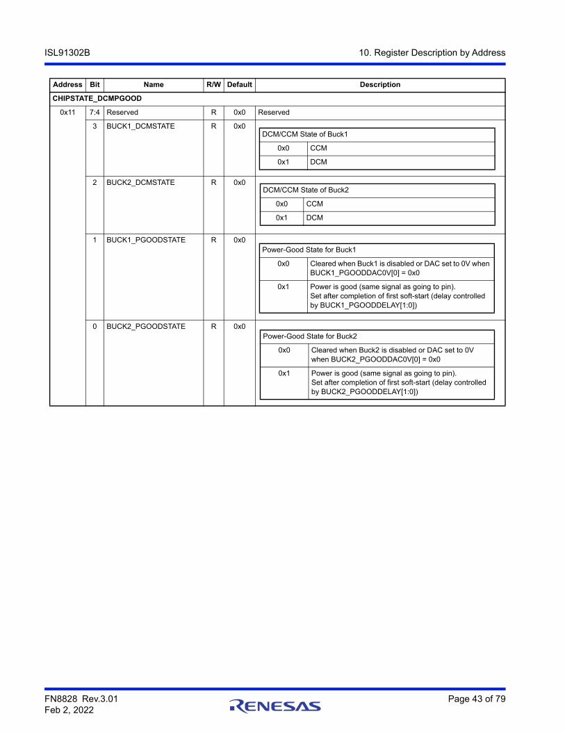
CHIPSTATE_DCMPGOOD
0x11 7:4 Reserved R 0x0 Reserved
3 BUCK1_DCMSTATE R 0x0
2 BUCK2_DCMSTATE R 0x0
1 BUCK1_PGOODSTATE R 0x0
0 BUCK2_PGOODSTATE R 0x0
Address Bit Name R/W Default Description
DCM/CCM State of Buck1
0x0 CCM
0x1 DCM
DCM/CCM State of Buck2
0x0 CCM
0x1 DCM
Power-Good State for Buck1
0x0 Cleared when Buck1 is disabled or DAC set to 0V when BUCK1_PGOODDAC0V[0] = 0x0
0x1 Power is good (same signal as going to pin).Set after completion of first soft-start (delay controlled by BUCK1_PGOODDELAY[1:0])
Power-Good State for Buck2
0x0 Cleared when Buck2 is disabled or DAC set to 0V when BUCK2_PGOODDAC0V[0] = 0x0
0x1 Power is good (same signal as going to pin).Set after completion of first soft-start (delay controlled by BUCK2_PGOODDELAY[1:0])
FN8828 Rev.3.01 Page 44 of 79Feb 2, 2022
ISL91302B 10. Register Description by Address
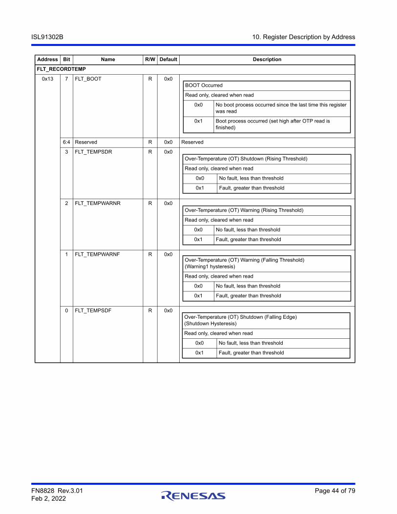
FLT_RECORDTEMP
0x13 7 FLT_BOOT R 0x0
6:4 Reserved R 0x0 Reserved
3 FLT_TEMPSDR R 0x0
2 FLT_TEMPWARNR R 0x0
1 FLT_TEMPWARNF R 0x0
0 FLT_TEMPSDF R 0x0
Address Bit Name R/W Default Description
BOOT Occurred
Read only, cleared when read
0x0 No boot process occurred since the last time this register was read
0x1 Boot process occurred (set high after OTP read is finished)
Over-Temperature (OT) Shutdown (Rising Threshold)
Read only, cleared when read
0x0 No fault, less than threshold
0x1 Fault, greater than threshold
Over-Temperature (OT) Warning (Rising Threshold)
Read only, cleared when read
0x0 No fault, less than threshold
0x1 Fault, greater than threshold
Over-Temperature (OT) Warning (Falling Threshold) (Warning1 hysteresis)
Read only, cleared when read
0x0 No fault, less than threshold
0x1 Fault, greater than threshold
Over-Temperature (OT) Shutdown (Falling Edge) (Shutdown Hysteresis)
Read only, cleared when read
0x0 No fault, less than threshold
0x1 Fault, greater than threshold
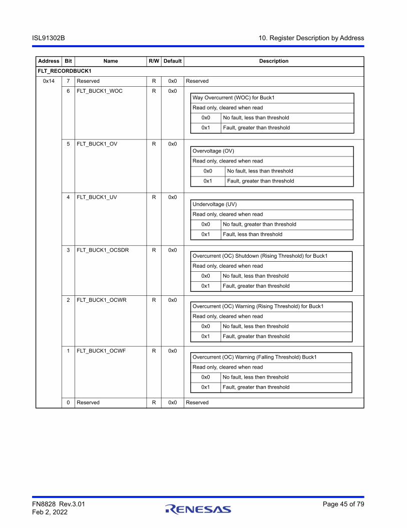
FN8828 Rev.3.01 Page 45 of 79Feb 2, 2022
ISL91302B 10. Register Description by Address
FLT_RECORDBUCK1
0x14 7 Reserved R 0x0 Reserved
6 FLT_BUCK1_WOC R 0x0
5 FLT_BUCK1_OV R 0x0
4 FLT_BUCK1_UV R 0x0
3 FLT_BUCK1_OCSDR R 0x0
2 FLT_BUCK1_OCWR R 0x0
1 FLT_BUCK1_OCWF R 0x0
0 Reserved R 0x0 Reserved
Address Bit Name R/W Default Description
Way Overcurrent (WOC) for Buck1
Read only, cleared when read
0x0 No fault, less than threshold
0x1 Fault, greater than threshold
Overvoltage (OV)
Read only, cleared when read
0x0 No fault, less than threshold
0x1 Fault, greater than threshold
Undervoltage (UV)
Read only, cleared when read
0x0 No fault, greater than threshold
0x1 Fault, less than threshold
Overcurrent (OC) Shutdown (Rising Threshold) for Buck1
Read only, cleared when read
0x0 No fault, less than threshold
0x1 Fault, greater than threshold
Overcurrent (OC) Warning (Rising Threshold) for Buck1
Read only, cleared when read
0x0 No fault, less then threshold
0x1 Fault, greater than threshold
Overcurrent (OC) Warning (Falling Threshold) Buck1
Read only, cleared when read
0x0 No fault, less then threshold
0x1 Fault, greater than threshold
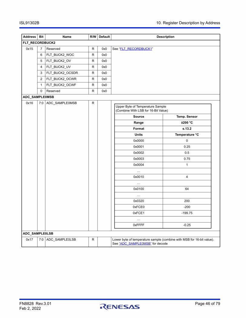
FN8828 Rev.3.01 Page 46 of 79Feb 2, 2022
ISL91302B 10. Register Description by Address
FLT_RECORDBUCK2
0x15 7 Reserved R 0x0 See “FLT_RECORDBUCK1”
6 FLT_BUCK2_WOC R 0x0
5 FLT_BUCK2_OV R 0x0
4 FLT_BUCK2_UV R 0x0
3 FLT_BUCK2_OCSDR R 0x0
2 FLT_BUCK2_OCWR R 0x0
1 FLT_BUCK2_OCWF R 0x0
0 Reserved R 0x0
ADC_SAMPLE0MSB
0x16 7:0 ADC_SAMPLE0MSB R
ADC_SAMPLE0LSB
0x17 7:0 ADC_SAMPLE0LSB R Lower byte of temperature sample (combine with MSB for 16-bit value).See “ADC_SAMPLE0MSB” for decode
Address Bit Name R/W Default Description
Upper Byte of Temperature Sample(Combine With LSB for 16-Bit Value)
Source Temp. Sensor
Range ±200 °C
Format s.13.2
Units Temperature °C
0x0000 0
0x0001 0.25
0x0002 0.5
0x0003 0.75
0x0004 1
…
0x0010 4
…
0x0100 64
…
0x0320 200
0xFCE0 -200
0xFCE1 -199.75
…
0xFFFF -0.25
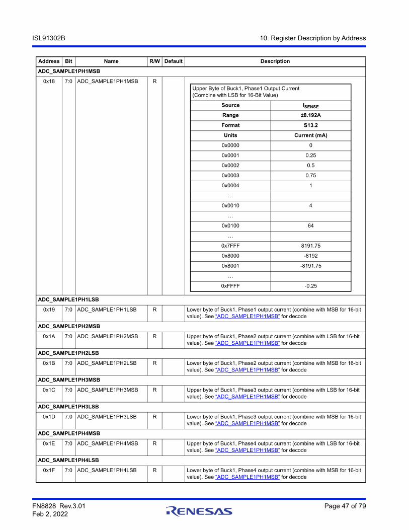
FN8828 Rev.3.01 Page 47 of 79Feb 2, 2022
ISL91302B 10. Register Description by Address
ADC_SAMPLE1PH1MSB
0x18 7:0 ADC_SAMPLE1PH1MSB R
ADC_SAMPLE1PH1LSB
0x19 7:0 ADC_SAMPLE1PH1LSB R Lower byte of Buck1, Phase1 output current (combine with MSB for 16-bit value). See “ADC_SAMPLE1PH1MSB” for decode
ADC_SAMPLE1PH2MSB
0x1A 7:0 ADC_SAMPLE1PH2MSB R Upper byte of Buck1, Phase2 output current (combine with LSB for 16-bit value). See “ADC_SAMPLE1PH1MSB” for decode
ADC_SAMPLE1PH2LSB
0x1B 7:0 ADC_SAMPLE1PH2LSB R Lower byte of Buck1, Phase2 output current (combine with MSB for 16-bit value). See “ADC_SAMPLE1PH1MSB” for decode
ADC_SAMPLE1PH3MSB
0x1C 7:0 ADC_SAMPLE1PH3MSB R Upper byte of Buck1, Phase3 output current (combine with LSB for 16-bit value). See “ADC_SAMPLE1PH1MSB” for decode
ADC_SAMPLE1PH3LSB
0x1D 7:0 ADC_SAMPLE1PH3LSB R Lower byte of Buck1, Phase3 output current (combine with MSB for 16-bit value). See “ADC_SAMPLE1PH1MSB” for decode
ADC_SAMPLE1PH4MSB
0x1E 7:0 ADC_SAMPLE1PH4MSB R Upper byte of Buck1, Phase4 output current (combine with LSB for 16-bit value). See “ADC_SAMPLE1PH1MSB” for decode
ADC_SAMPLE1PH4LSB
0x1F 7:0 ADC_SAMPLE1PH4LSB R Lower byte of Buck1, Phase4 output current (combine with MSB for 16-bit value). See “ADC_SAMPLE1PH1MSB” for decode
Address Bit Name R/W Default Description
Upper Byte of Buck1, Phase1 Output Current(Combine with LSB for 16-Bit Value)
Source ISENSE
Range ±8.192A
Format S13.2
Units Current (mA)
0x0000 0
0x0001 0.25
0x0002 0.5
0x0003 0.75
0x0004 1
…
0x0010 4
…
0x0100 64
…
0x7FFF 8191.75
0x8000 -8192
0x8001 -8191.75
…
0xFFFF -0.25
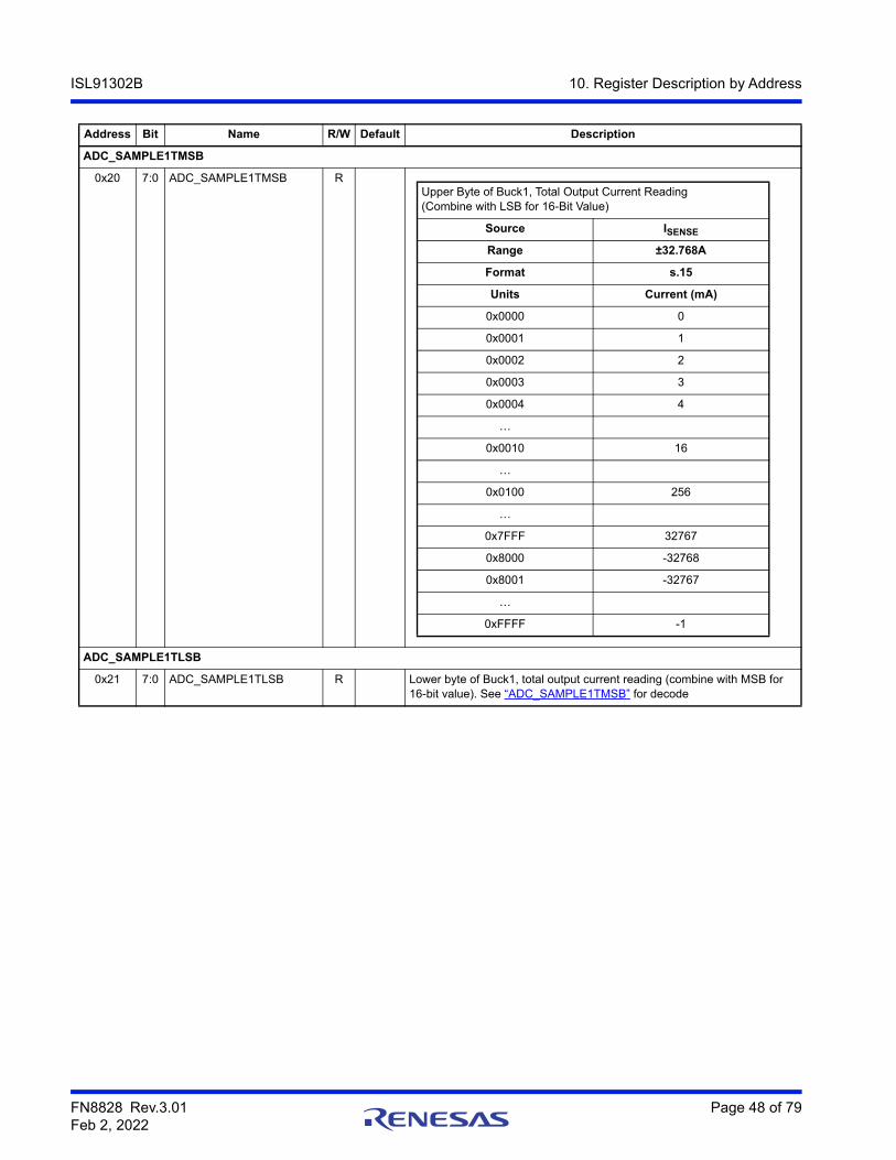
FN8828 Rev.3.01 Page 48 of 79Feb 2, 2022
ISL91302B 10. Register Description by Address
ADC_SAMPLE1TMSB
0x20 7:0 ADC_SAMPLE1TMSB R
ADC_SAMPLE1TLSB
0x21 7:0 ADC_SAMPLE1TLSB R Lower byte of Buck1, total output current reading (combine with MSB for 16-bit value). See “ADC_SAMPLE1TMSB” for decode
Address Bit Name R/W Default Description
Upper Byte of Buck1, Total Output Current Reading(Combine with LSB for 16-Bit Value)
Source ISENSE
Range ±32.768A
Format s.15
Units Current (mA)
0x0000 0
0x0001 1
0x0002 2
0x0003 3
0x0004 4
…
0x0010 16
…
0x0100 256
…
0x7FFF 32767
0x8000 -32768
0x8001 -32767
…
0xFFFF -1

FN8828 Rev.3.01 Page 49 of 79Feb 2, 2022
ISL91302B 10. Register Description by Address
ADC_SAMPLE2MSB
0x22 7:0 ADC_SAMPLE2MSB R
ADC_SAMPLE2LSB
0x23 7:0 ADC_SAMPLE2LSB R Lower byte of Buck1 PVIN reading (combine with MSB for 16-bit value).See “ADC_SAMPLE2MSB” for decode
Address Bit Name R/W Default Description
Upper Byte of Buck1, PVIN Sample(Combine with LSB for 16-Bit Value)
Source PVIN
Range ±8.192V
Format s.13.2
Units Voltage (mV)
0x0000 0
0x0001 0.25
0x0002 0.5
0x0003 0.75
0x0004 1
…
0x0010 4
…
0x0100 64
…
0x7FFF 8191.75
0x8000 -8192
0x8001 -8191.75
…
0xFFFF -0.25
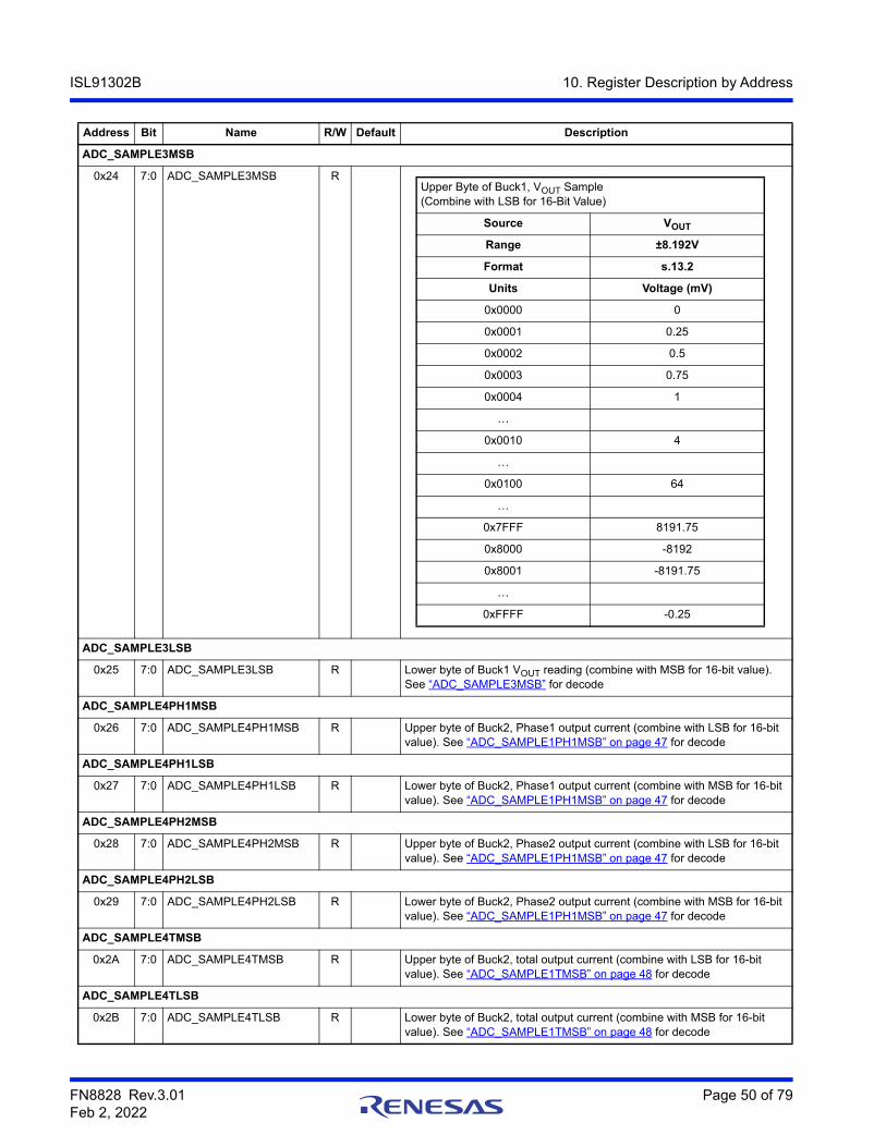
FN8828 Rev.3.01 Page 50 of 79Feb 2, 2022
ISL91302B 10. Register Description by Address
ADC_SAMPLE3MSB
0x24 7:0 ADC_SAMPLE3MSB R
ADC_SAMPLE3LSB
0x25 7:0 ADC_SAMPLE3LSB R Lower byte of Buck1 VOUT reading (combine with MSB for 16-bit value).See “ADC_SAMPLE3MSB” for decode
ADC_SAMPLE4PH1MSB
0x26 7:0 ADC_SAMPLE4PH1MSB R Upper byte of Buck2, Phase1 output current (combine with LSB for 16-bit value). See “ADC_SAMPLE1PH1MSB” on page 47 for decode
ADC_SAMPLE4PH1LSB
0x27 7:0 ADC_SAMPLE4PH1LSB R Lower byte of Buck2, Phase1 output current (combine with MSB for 16-bit value). See “ADC_SAMPLE1PH1MSB” on page 47 for decode
ADC_SAMPLE4PH2MSB
0x28 7:0 ADC_SAMPLE4PH2MSB R Upper byte of Buck2, Phase2 output current (combine with LSB for 16-bit value). See “ADC_SAMPLE1PH1MSB” on page 47 for decode
ADC_SAMPLE4PH2LSB
0x29 7:0 ADC_SAMPLE4PH2LSB R Lower byte of Buck2, Phase2 output current (combine with MSB for 16-bit value). See “ADC_SAMPLE1PH1MSB” on page 47 for decode
ADC_SAMPLE4TMSB
0x2A 7:0 ADC_SAMPLE4TMSB R Upper byte of Buck2, total output current (combine with LSB for 16-bit value). See “ADC_SAMPLE1TMSB” on page 48 for decode
ADC_SAMPLE4TLSB
0x2B 7:0 ADC_SAMPLE4TLSB R Lower byte of Buck2, total output current (combine with MSB for 16-bit value). See “ADC_SAMPLE1TMSB” on page 48 for decode
Address Bit Name R/W Default Description
Upper Byte of Buck1, VOUT Sample(Combine with LSB for 16-Bit Value)
Source VOUT
Range ±8.192V
Format s.13.2
Units Voltage (mV)
0x0000 0
0x0001 0.25
0x0002 0.5
0x0003 0.75
0x0004 1
…
0x0010 4
…
0x0100 64
…
0x7FFF 8191.75
0x8000 -8192
0x8001 -8191.75
…
0xFFFF -0.25
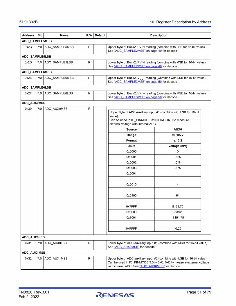
FN8828 Rev.3.01 Page 51 of 79Feb 2, 2022
ISL91302B 10. Register Description by Address
ADC_SAMPLE5MSB
0x2C 7:0 ADC_SAMPLE5MSB R Upper byte of Buck2, PVIN reading (combine with LSB for 16-bit value).See “ADC_SAMPLE2MSB” on page 49 for decode
ADC_SAMPLE5LSB
0x2D 7:0 ADC_SAMPLE5LSB R Lower byte of Buck2, PVIN reading (combine with MSB for 16-bit value).See “ADC_SAMPLE2MSB” on page 49 for decode
ADC_SAMPLE6MSB
0x2E 7:0 ADC_SAMPLE6MSB R Upper byte of Buck2, VOUT reading (Combine with LSB for 16-bit value).See “ADC_SAMPLE3MSB” on page 50 for decode
ADC_SAMPLE6LSB
0x2F 7:0 ADC_SAMPLE6LSB R Lower byte of Buck2, VOUT reading (combine with MSB for 16-bit value).See “ADC_SAMPLE3MSB” on page 50 for decode.
ADC_AUX0MSB
0x30 7:0 ADC_AUX0MSB R
ADC_AUX0LSB
0x31 7:0 ADC_AUX0LSB R Lower byte of ADC auxiliary input #1 (combine with MSB for 16-bit value).See “ADC_AUX0MSB” for decode
ADC_AUX1MSB
0x32 7:0 ADC_AUX1MSB R Upper byte of ADC auxiliary input #2 (combine with LSB for 16-bit value).Can be used in IO_PINMODE[3:0] = 0xC, 0xD to measure external voltage with internal ADC. See “ADC_AUX0MSB” for decode
Address Bit Name R/W Default Description
Upper Byte of ADC Auxiliary Input #1 (combine with LSB for 16-bit value).Can be used in IO_PINMODE[3:0] = 0xC, 0xD to measure external voltage with internal ADC.
Source AUX0
Range ±8.192V
Format s.13.2
Units Voltage (mV)
0x0000 0
0x0001 0.25
0x0002 0.5
0x0003 0.75
0x0004 1
…
0x0010 4
…
0x0100 64
…
0x7FFF 8191.75
0x8000 -8192
0x8001 -8191.75
…
0xFFFF -0.25
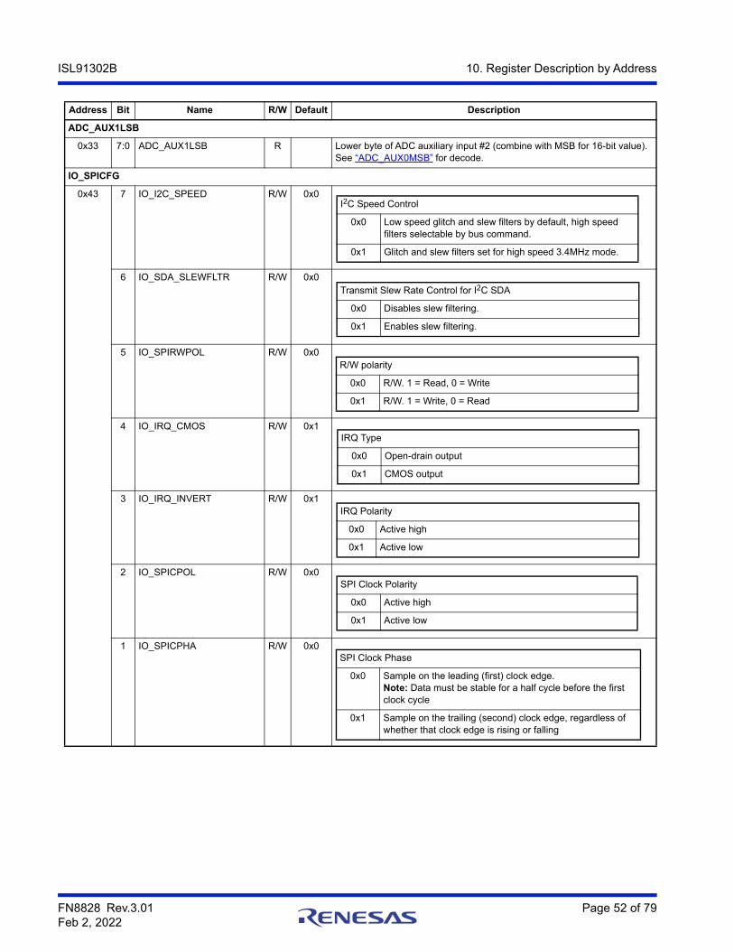
FN8828 Rev.3.01 Page 52 of 79Feb 2, 2022
ISL91302B 10. Register Description by Address
ADC_AUX1LSB
0x33 7:0 ADC_AUX1LSB R Lower byte of ADC auxiliary input #2 (combine with MSB for 16-bit value).See “ADC_AUX0MSB” for decode.
IO_SPICFG
0x43 7 IO_I2C_SPEED R/W 0x0
6 IO_SDA_SLEWFLTR R/W 0x0
5 IO_SPIRWPOL R/W 0x0
4 IO_IRQ_CMOS R/W 0x1
3 IO_IRQ_INVERT R/W 0x1
2 IO_SPICPOL R/W 0x0
1 IO_SPICPHA R/W 0x0
Address Bit Name R/W Default Description
I2C Speed Control
0x0 Low speed glitch and slew filters by default, high speed filters selectable by bus command.
0x1 Glitch and slew filters set for high speed 3.4MHz mode.
Transmit Slew Rate Control for I2C SDA
0x0 Disables slew filtering.
0x1 Enables slew filtering.
R/W polarity
0x0 R/W. 1 = Read, 0 = Write
0x1 R/W. 1 = Write, 0 = Read
IRQ Type
0x0 Open-drain output
0x1 CMOS output
IRQ Polarity
0x0 Active high
0x1 Active low
SPI Clock Polarity
0x0 Active high
0x1 Active low
SPI Clock Phase
0x0 Sample on the leading (first) clock edge.Note: Data must be stable for a half cycle before the first clock cycle
0x1 Sample on the trailing (second) clock edge, regardless of whether that clock edge is rising or falling
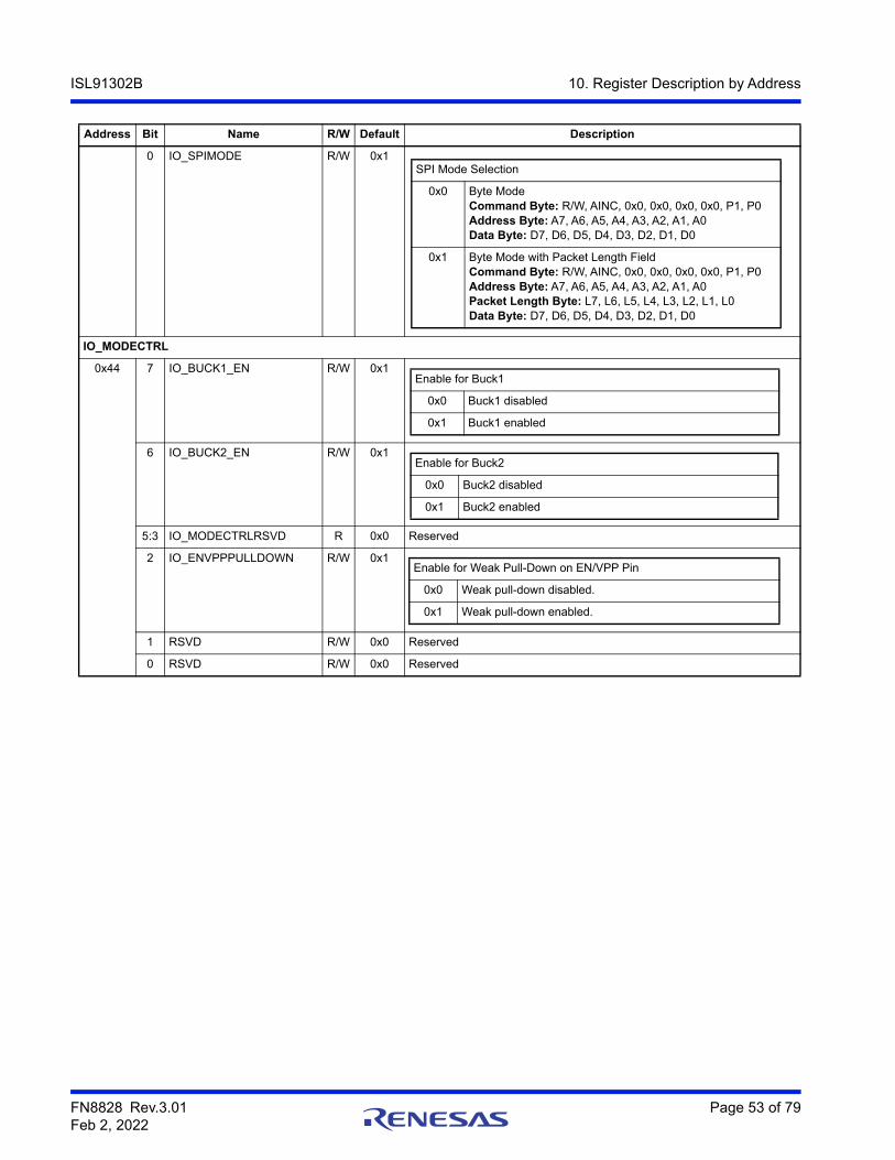
FN8828 Rev.3.01 Page 53 of 79Feb 2, 2022
ISL91302B 10. Register Description by Address
0 IO_SPIMODE R/W 0x1
IO_MODECTRL
0x44 7 IO_BUCK1_EN R/W 0x1
6 IO_BUCK2_EN R/W 0x1
5:3 IO_MODECTRLRSVD R 0x0 Reserved
2 IO_ENVPPPULLDOWN R/W 0x1
1 RSVD R/W 0x0 Reserved
0 RSVD R/W 0x0 Reserved
Address Bit Name R/W Default Description
SPI Mode Selection
0x0 Byte ModeCommand Byte: R/W, AINC, 0x0, 0x0, 0x0, 0x0, P1, P0Address Byte: A7, A6, A5, A4, A3, A2, A1, A0Data Byte: D7, D6, D5, D4, D3, D2, D1, D0
0x1 Byte Mode with Packet Length FieldCommand Byte: R/W, AINC, 0x0, 0x0, 0x0, 0x0, P1, P0Address Byte: A7, A6, A5, A4, A3, A2, A1, A0Packet Length Byte: L7, L6, L5, L4, L3, L2, L1, L0Data Byte: D7, D6, D5, D4, D3, D2, D1, D0
Enable for Buck1
0x0 Buck1 disabled
0x1 Buck1 enabled
Enable for Buck2
0x0 Buck2 disabled
0x1 Buck2 enabled
Enable for Weak Pull-Down on EN/VPP Pin
0x0 Weak pull-down disabled.
0x1 Weak pull-down enabled.
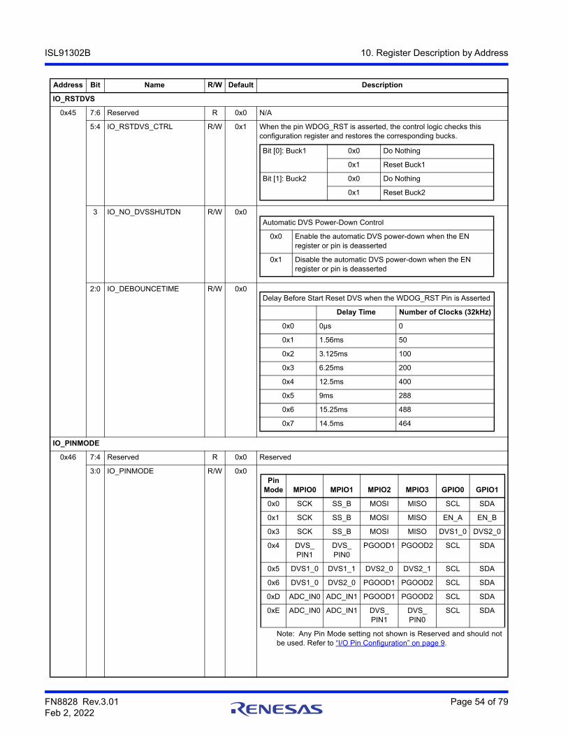
FN8828 Rev.3.01 Page 54 of 79Feb 2, 2022
ISL91302B 10. Register Description by Address
IO_RSTDVS
0x45 7:6 Reserved R 0x0 N/A
5:4 IO_RSTDVS_CTRL R/W 0x1 When the pin WDOG_RST is asserted, the control logic checks this configuration register and restores the corresponding bucks.
3 IO_NO_DVSSHUTDN R/W 0x0
2:0 IO_DEBOUNCETIME R/W 0x0
IO_PINMODE
0x46 7:4 Reserved R 0x0 Reserved
3:0 IO_PINMODE R/W 0x0
Address Bit Name R/W Default Description
Bit [0]: Buck1 0x0 Do Nothing
0x1 Reset Buck1
Bit [1]: Buck2 0x0 Do Nothing
0x1 Reset Buck2
Automatic DVS Power-Down Control
0x0 Enable the automatic DVS power-down when the EN register or pin is deasserted
0x1 Disable the automatic DVS power-down when the EN register or pin is deasserted
Delay Before Start Reset DVS when the WDOG_RST Pin is Asserted
Delay Time Number of Clocks (32kHz)
0x0 0µs 0
0x1 1.56ms 50
0x2 3.125ms 100
0x3 6.25ms 200
0x4 12.5ms 400
0x5 9ms 288
0x6 15.25ms 488
0x7 14.5ms 464
Pin Mode MPIO0 MPIO1 MPIO2 MPIO3 GPIO0 GPIO1
0x0 SCK SS_B MOSI MISO SCL SDA
0x1 SCK SS_B MOSI MISO EN_A EN_B
0x3 SCK SS_B MOSI MISO DVS1_0 DVS2_0
0x4 DVS_PIN1
DVS_PIN0
PGOOD1 PGOOD2 SCL SDA
0x5 DVS1_0 DVS1_1 DVS2_0 DVS2_1 SCL SDA
0x6 DVS1_0 DVS2_0 PGOOD1 PGOOD2 SCL SDA
0xD ADC_IN0 ADC_IN1 PGOOD1 PGOOD2 SCL SDA
0xE ADC_IN0 ADC_IN1 DVS_PIN1
DVS_PIN0
SCL SDA
Note: Any Pin Mode setting not shown is Reserved and should notbe used. Refer to “I/O Pin Configuration” on page 9.

FN8828 Rev.3.01 Page 55 of 79Feb 2, 2022
ISL91302B 10. Register Description by Address
ADC_RATECCMDCM
0x50 7:4 ADC_RATECCM R/W 0x3
3:0 ADC_RATEDCM R/W 0x5
Address Bit Name R/W Default Description
Sampling period when either one of the buck outputs is in CCM.
0x0 Off or One-shot Mode
0x1 31.25µs
0x2 62.5µs
0x3 125µs
0x4 250µs
0x5 500µs
0x6 1ms
0x7 2ms
0x8 4ms
0x9 8ms
0xA 16ms
0xB 32ms
0xC 64ms
0xD 128ms
0xE 256ms
0xF 512ms
Sampling period when both buck outputs are in DCM.
0x0 Off or One-shot Mode
0x1 31.25µs
0x2 62.5µs
0x3 125µs
0x4 250µs
0x5 500µs
0x6 1ms
0x7 2ms
0x8 4ms
0x9 8ms
0xA 16ms
0xB 32ms
0xC 64ms
0xD 128ms
0xE 256ms
0xF 512ms
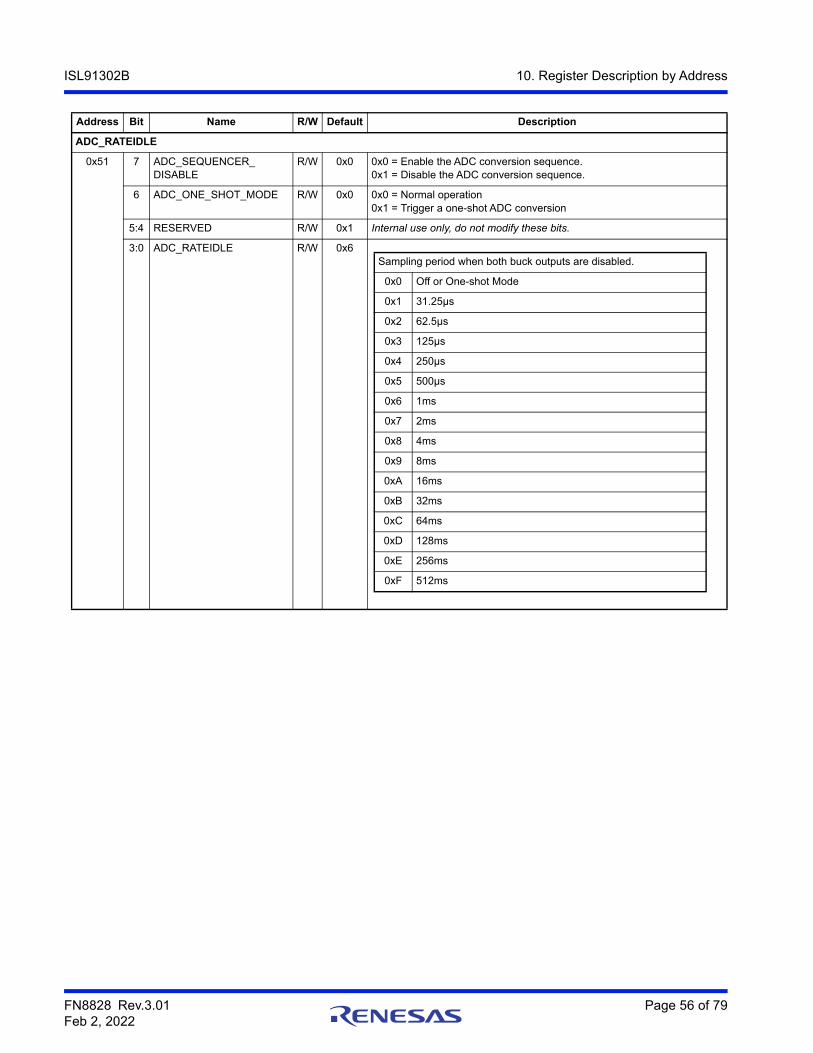
FN8828 Rev.3.01 Page 56 of 79Feb 2, 2022
ISL91302B 10. Register Description by Address
ADC_RATEIDLE
0x51 7 ADC_SEQUENCER_DISABLE
R/W 0x0 0x0 = Enable the ADC conversion sequence.0x1 = Disable the ADC conversion sequence.
6 ADC_ONE_SHOT_MODE R/W 0x0 0x0 = Normal operation0x1 = Trigger a one-shot ADC conversion
5:4 RESERVED R/W 0x1 Internal use only, do not modify these bits.
3:0 ADC_RATEIDLE R/W 0x6
Address Bit Name R/W Default Description
Sampling period when both buck outputs are disabled.
0x0 Off or One-shot Mode
0x1 31.25µs
0x2 62.5µs
0x3 125µs
0x4 250µs
0x5 500µs
0x6 1ms
0x7 2ms
0x8 4ms
0x9 8ms
0xA 16ms
0xB 32ms
0xC 64ms
0xD 128ms
0xE 256ms
0xF 512ms
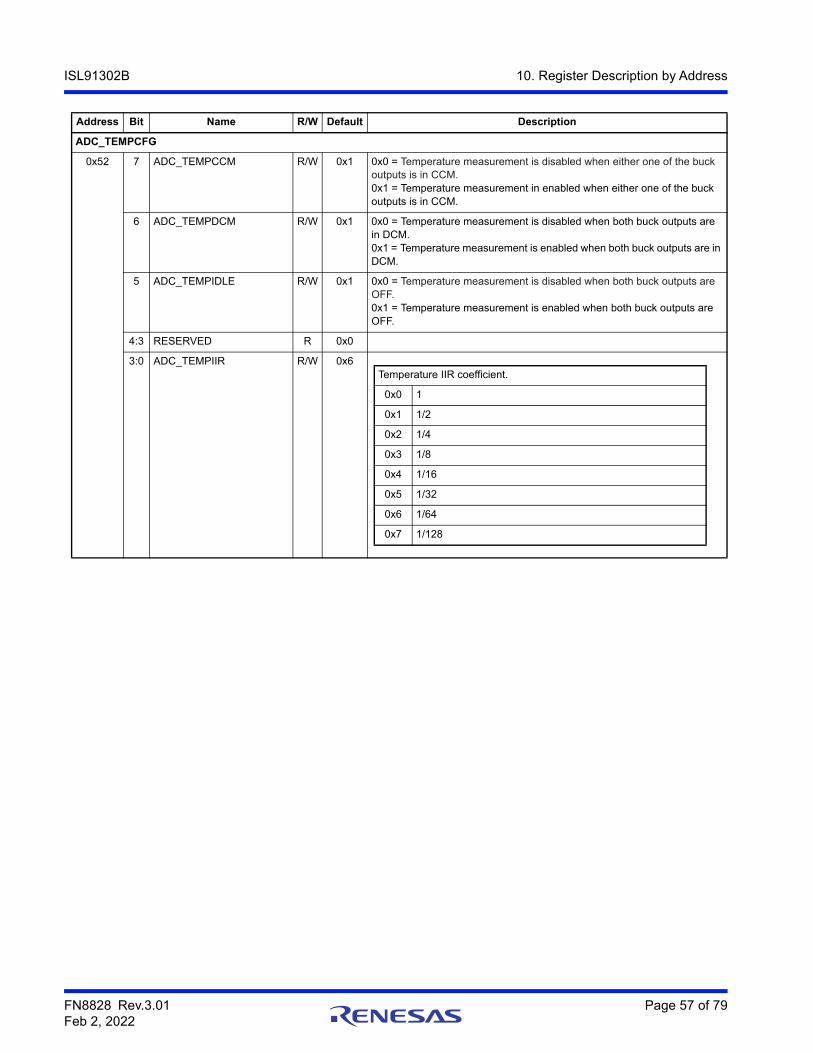
FN8828 Rev.3.01 Page 57 of 79Feb 2, 2022
ISL91302B 10. Register Description by Address
ADC_TEMPCFG
0x52 7 ADC_TEMPCCM R/W 0x1 0x0 = Temperature measurement is disabled when either one of the buck outputs is in CCM.0x1 = Temperature measurement in enabled when either one of the buck outputs is in CCM.
6 ADC_TEMPDCM R/W 0x1 0x0 = Temperature measurement is disabled when both buck outputs are in DCM.0x1 = Temperature measurement is enabled when both buck outputs are in DCM.
5 ADC_TEMPIDLE R/W 0x1 0x0 = Temperature measurement is disabled when both buck outputs are OFF.0x1 = Temperature measurement is enabled when both buck outputs are OFF.
4:3 RESERVED R 0x0
3:0 ADC_TEMPIIR R/W 0x6
Address Bit Name R/W Default Description
Temperature IIR coefficient.
0x0 1
0x1 1/2
0x2 1/4
0x3 1/8
0x4 1/16
0x5 1/32
0x6 1/64
0x7 1/128
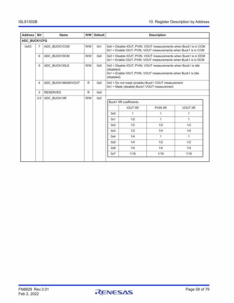
FN8828 Rev.3.01 Page 58 of 79Feb 2, 2022
ISL91302B 10. Register Description by Address
ADC_BUCK1CFG
0x53 7 ADC_BUCK1CCM R/W 0x1 0x0 = Disable IOUT, PVIN, VOUT measurements when Buck1 is in CCM0x1 = Enable IOUT, PVIN, VOUT measurements when Buck1 is in CCM
6 ADC_BUCK1DCM R/W 0x0 0x0 = Disable IOUT, PVIN, VOUT measurements when Buck1 is in DCM0x1 = Enable IOUT, PVIN, VOUT measurements when Buck1 is in DCM
5 ADC_BUCK1IDLE R/W 0x0 0x0 = Disable IOUT, PVIN, VOUT measurements when Buck1 is idle (disabled)0x1 = Enable IOUT, PVIN, VOUT measurements when Buck1 is idle (disabled)
4 ADC_BUCK1MASKVOUT R 0x0 0x0 = Do not mask (enable) Buck1 VOUT measurement0x1 = Mask (disable) Buck1 VOUT measurement
3 RESERVED R 0x0
2:0 ADC_BUCK1IIR R/W 0x2
Address Bit Name R/W Default Description
Buck1 IIR coefficients.
IOUT IIR PVIN IIR VOUT IIR
0x0 1 1 1
0x1 1/2 1 1
0x2 1/2 1/2 1/2
0x3 1/2 1/4 1/4
0x4 1/4 1 1
0x5 1/4 1/2 1/2
0x6 1/4 1/4 1/4
0x7 1/16 1/16 1/16

FN8828 Rev.3.01 Page 59 of 79Feb 2, 2022
ISL91302B 10. Register Description by Address
ADC_BUCK2CFG
0x54 7 ADC_BUCK2CCM R/W 0x1 0x0 = Disable IOUT, PVIN, VOUT measurements when Buck2 is in CCM0x1 = Enable IOUT, PVIN, VOUT measurements when Buck2 is in CCM
6 ADC_BUCK2DCM R/W 0x0 0x0 = Disable IOUT, PVIN, VOUT measurements when Buck2 is in DCM0x1 = Enable IOUT, PVIN, VOUT measurements when Buck2 is in DCM
5 ADC_BUCK2IDLE R/W 0x0 0x0 = Disable IOUT, PVIN, VOUT measurements when Buck2 is idle (disabled)0x1 = Enable IOUT, PVIN, VOUT measurements when Buck2 is idle (disabled)
4 ADC_BUCK2MASKVOUT R 0x0 0x0 = Do not mask (enable) Buck2 VOUT measurement0x1 = Mask (disable) Buck2 VOUT measurement
3 RESERVED R 0x0
2:0 ADC_BUCK2IIR R/W 0x2
Address Bit Name R/W Default Description
Buck2 IIR coefficients.
IOUT IIR PVIN IIR VOUT IIR
0x0 1 1 1
0x1 1/2 1 1
0x2 1/2 1/2 1/2
0x3 1/2 1/4 1/4
0x4 1/4 1 1
0x5 1/4 1/2 1/2
0x6 1/4 1/4 1/4
0x7 1/16 1/16 1/16
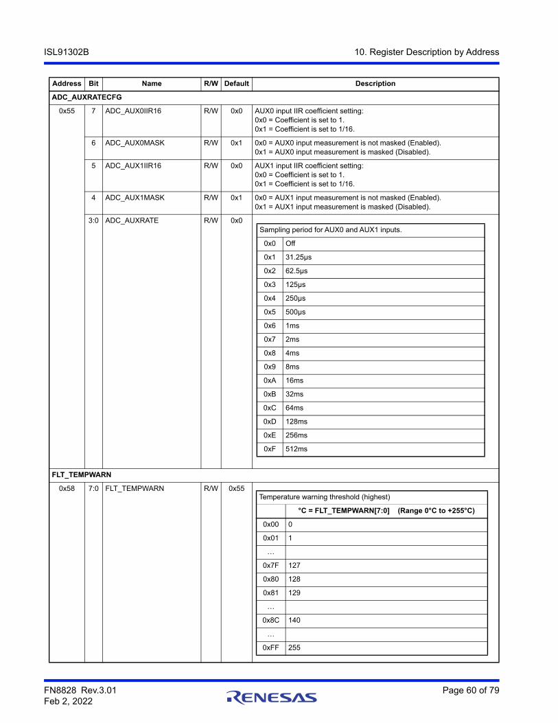
FN8828 Rev.3.01 Page 60 of 79Feb 2, 2022
ISL91302B 10. Register Description by Address
ADC_AUXRATECFG
0x55 7 ADC_AUX0IIR16 R/W 0x0 AUX0 input IIR coefficient setting:0x0 = Coefficient is set to 1.0x1 = Coefficient is set to 1/16.
6 ADC_AUX0MASK R/W 0x1 0x0 = AUX0 input measurement is not masked (Enabled).0x1 = AUX0 input measurement is masked (Disabled).
5 ADC_AUX1IIR16 R/W 0x0 AUX1 input IIR coefficient setting:0x0 = Coefficient is set to 1.0x1 = Coefficient is set to 1/16.
4 ADC_AUX1MASK R/W 0x1 0x0 = AUX1 input measurement is not masked (Enabled).0x1 = AUX1 input measurement is masked (Disabled).
3:0 ADC_AUXRATE R/W 0x0
FLT_TEMPWARN
0x58 7:0 FLT_TEMPWARN R/W 0x55
Address Bit Name R/W Default Description
Sampling period for AUX0 and AUX1 inputs.
0x0 Off
0x1 31.25µs
0x2 62.5µs
0x3 125µs
0x4 250µs
0x5 500µs
0x6 1ms
0x7 2ms
0x8 4ms
0x9 8ms
0xA 16ms
0xB 32ms
0xC 64ms
0xD 128ms
0xE 256ms
0xF 512ms
Temperature warning threshold (highest)
°C = FLT_TEMPWARN[7:0] (Range 0°C to +255°C)
0x00 0
0x01 1
…
0x7F 127
0x80 128
0x81 129
…
0x8C 140
…
0xFF 255
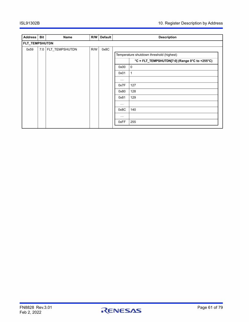
FN8828 Rev.3.01 Page 61 of 79Feb 2, 2022
ISL91302B 10. Register Description by Address
FLT_TEMPSHUTDN
0x59 7:0 FLT_TEMPSHUTDN R/W 0x8C
Address Bit Name R/W Default Description
Temperature shutdown threshold (highest)
°C = FLT_TEMPSHUTDN[7:0] (Range 0°C to +255°C)
0x00 0
0x01 1
…
0x7F 127
0x80 128
0x81 129
…
0x8C 140
…
0xFF 255
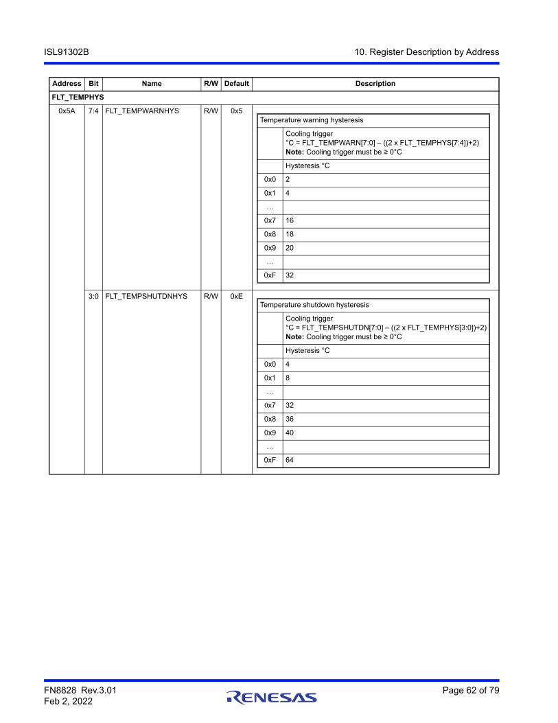
FN8828 Rev.3.01 Page 62 of 79Feb 2, 2022
ISL91302B 10. Register Description by Address
FLT_TEMPHYS
0x5A 7:4 FLT_TEMPWARNHYS R/W 0x5
3:0 FLT_TEMPSHUTDNHYS R/W 0xE
Address Bit Name R/W Default Description
Temperature warning hysteresis
Cooling trigger °C = FLT_TEMPWARN[7:0] – ((2 x FLT_TEMPHYS[7:4])+2)Note: Cooling trigger must be ≥ 0°C
Hysteresis °C
0x0 2
0x1 4
…
0x7 16
0x8 18
0x9 20
…
0xF 32
Temperature shutdown hysteresis
Cooling trigger °C = FLT_TEMPSHUTDN[7:0] – ((2 x FLT_TEMPHYS[3:0])+2)Note: Cooling trigger must be ≥ 0°C
Hysteresis °C
0x0 4
0x1 8
…
0x7 32
0x8 36
0x9 40
…
0xF 64
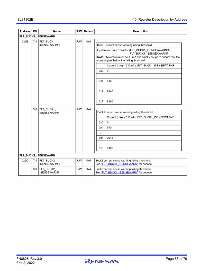
FN8828 Rev.3.01 Page 63 of 79Feb 2, 2022
ISL91302B 10. Register Description by Address
FLT_BUCK1_ISENSEWARN
0x5B 7:4 FLT_BUCK1_ISENSEWARNR
R/W 0x5
3:0 FLT_BUCK1_ISENSEWARNF
R/W 0x4
FLT_BUCK2_ISENSEWARN
0x5C 7:4 FLT_BUCK2_ISENSEWARNR
R/W 0x5 Buck2 current sense warning rising threshold.See “FLT_BUCK1_ISENSEWARN” for decode
3:0 FLT_BUCK2_ISENSEWARNF
R/W 0x4 Buck2 current sense warning falling threshold.See “FLT_BUCK1_ISENSEWARN” for decode
Address Bit Name R/W Default Description
Buck1 current sense warning rising threshold
Hysteresis mA = 512mA x (FLT_BUCK1_ISENSEAWARNR– FLT_BUCK1_ISENSEAWARNF)Note: Hysteresis must be ≥ 0mA and small enough to ensure that the current goes below the falling threshold.
Current (mA) = 512mA x FLT_BUCK1_ISENSEWARNR
0x0 0
0x1 510
…
0x4 2048
…
0xF 8160
Buck1 current sense warning falling threshold
Current (mA) = 510mA x FLT_BUCK1_ISENSEWARNF
0x0 0
0x1 510
…
0x4 2048
…
0xF 8160
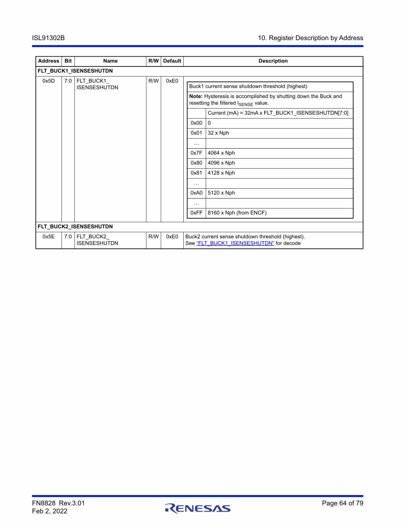
FN8828 Rev.3.01 Page 64 of 79Feb 2, 2022
ISL91302B 10. Register Description by Address
FLT_BUCK1_ISENSESHUTDN
0x5D 7:0 FLT_BUCK1_ISENSESHUTDN
R/W 0xE0
FLT_BUCK2_ISENSESHUTDN
0x5E 7:0 FLT_BUCK2_ISENSESHUTDN
R/W 0xE0 Buck2 current sense shutdown threshold (highest).See “FLT_BUCK1_ISENSESHUTDN” for decode
Address Bit Name R/W Default Description
Buck1 current sense shutdown threshold (highest)
Note: Hysteresis is accomplished by shutting down the Buck and resetting the filtered ISENSE value.
Current (mA) = 32mA x FLT_BUCK1_ISENSESHUTDN[7:0]
0x00 0
0x01 32 x Nph
…
0x7F 4064 x Nph
0x80 4096 x Nph
0x81 4128 x Nph
…
0xA0 5120 x Nph
…
0xFF 8160 x Nph (from ENCF)
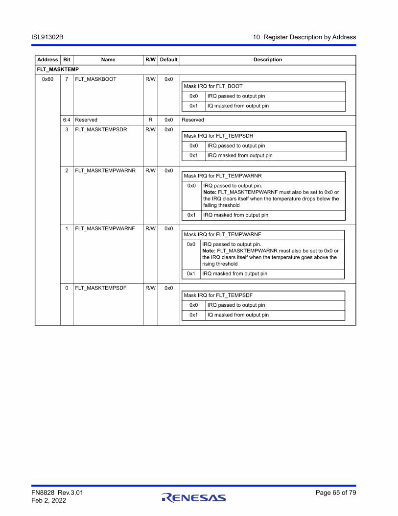
FN8828 Rev.3.01 Page 65 of 79Feb 2, 2022
ISL91302B 10. Register Description by Address
FLT_MASKTEMP
0x60 7 FLT_MASKBOOT R/W 0x0
6:4 Reserved R 0x0 Reserved
3 FLT_MASKTEMPSDR R/W 0x0
2 FLT_MASKTEMPWARNR R/W 0x0
1 FLT_MASKTEMPWARNF R/W 0x0
0 FLT_MASKTEMPSDF R/W 0x0
Address Bit Name R/W Default Description
Mask IRQ for FLT_BOOT
0x0 IRQ passed to output pin
0x1 IQ masked from output pin
Mask IRQ for FLT_TEMPSDR
0x0 IRQ passed to output pin
0x1 IRQ masked from output pin
Mask IRQ for FLT_TEMPWARNR
0x0 IRQ passed to output pin.Note: FLT_MASKTEMPWARNF must also be set to 0x0 or the IRQ clears itself when the temperature drops below the falling threshold
0x1 IRQ masked from output pin
Mask IRQ for FLT_TEMPWARNF
0x0 IRQ passed to output pin.Note: FLT_MASKTEMPWARNR must also be set to 0x0 or the IRQ clears itself when the temperature goes above the rising threshold
0x1 IRQ masked from output pin
Mask IRQ for FLT_TEMPSDF
0x0 IRQ passed to output pin
0x1 IQ masked from output pin
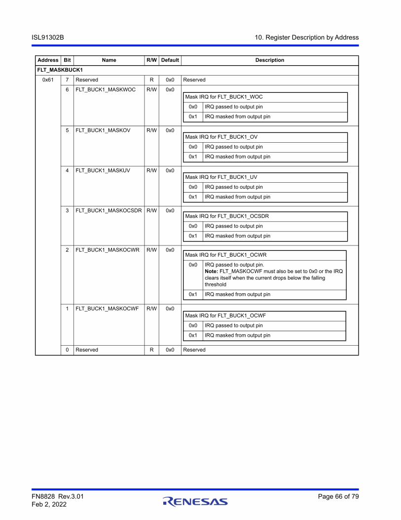
FN8828 Rev.3.01 Page 66 of 79Feb 2, 2022
ISL91302B 10. Register Description by Address
FLT_MASKBUCK1
0x61 7 Reserved R 0x0 Reserved
6 FLT_BUCK1_MASKWOC R/W 0x0
5 FLT_BUCK1_MASKOV R/W 0x0
4 FLT_BUCK1_MASKUV R/W 0x0
3 FLT_BUCK1_MASKOCSDR R/W 0x0
2 FLT_BUCK1_MASKOCWR R/W 0x0
1 FLT_BUCK1_MASKOCWF R/W 0x0
0 Reserved R 0x0 Reserved
Address Bit Name R/W Default Description
Mask IRQ for FLT_BUCK1_WOC
0x0 IRQ passed to output pin
0x1 IRQ masked from output pin
Mask IRQ for FLT_BUCK1_OV
0x0 IRQ passed to output pin
0x1 IRQ masked from output pin
Mask IRQ for FLT_BUCK1_UV
0x0 IRQ passed to output pin
0x1 IRQ masked from output pin
Mask IRQ for FLT_BUCK1_OCSDR
0x0 IRQ passed to output pin
0x1 IRQ masked from output pin
Mask IRQ for FLT_BUCK1_OCWR
0x0 IRQ passed to output pin.Note: FLT_MASKOCWF must also be set to 0x0 or the IRQ clears itself when the current drops below the falling threshold
0x1 IRQ masked from output pin
Mask IRQ for FLT_BUCK1_OCWF
0x0 IRQ passed to output pin
0x1 IRQ masked from output pin
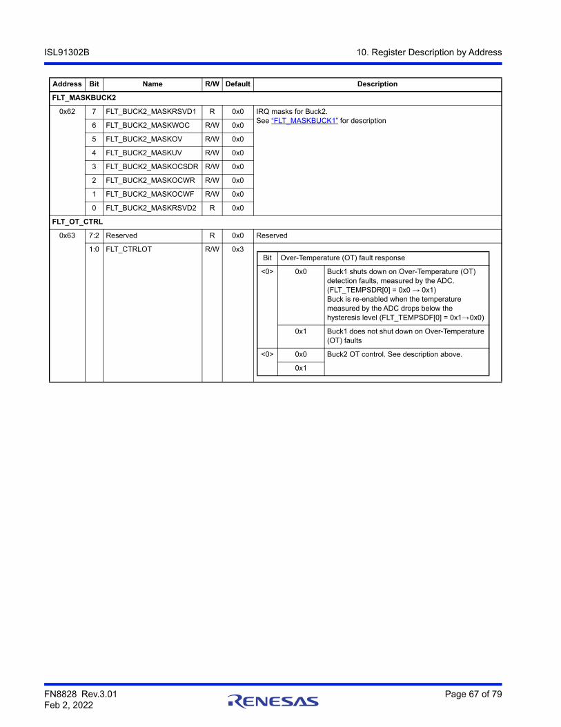
FN8828 Rev.3.01 Page 67 of 79Feb 2, 2022
ISL91302B 10. Register Description by Address
FLT_MASKBUCK2
0x62 7 FLT_BUCK2_MASKRSVD1 R 0x0 IRQ masks for Buck2.See “FLT_MASKBUCK1” for description
6 FLT_BUCK2_MASKWOC R/W 0x0
5 FLT_BUCK2_MASKOV R/W 0x0
4 FLT_BUCK2_MASKUV R/W 0x0
3 FLT_BUCK2_MASKOCSDR R/W 0x0
2 FLT_BUCK2_MASKOCWR R/W 0x0
1 FLT_BUCK2_MASKOCWF R/W 0x0
0 FLT_BUCK2_MASKRSVD2 R 0x0
FLT_OT_CTRL
0x63 7:2 Reserved R 0x0 Reserved
1:0 FLT_CTRLOT R/W 0x3
Address Bit Name R/W Default Description
Bit Over-Temperature (OT) fault response
<0> 0x0 Buck1 shuts down on Over-Temperature (OT) detection faults, measured by the ADC. (FLT_TEMPSDR[0] = 0x0 → 0x1)Buck is re-enabled when the temperature measured by the ADC drops below the hysteresis level (FLT_TEMPSDF[0] = 0x1→0x0)
0x1 Buck1 does not shut down on Over-Temperature (OT) faults
<0> 0x0 Buck2 OT control. See description above.
0x1
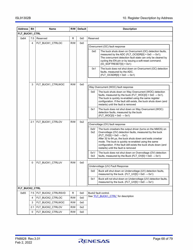
FN8828 Rev.3.01 Page 68 of 79Feb 2, 2022
ISL91302B 10. Register Description by Address
FLT_BUCK1_CTRL
0x64 7:5 Reserved R 0x0 Reserved
4 FLT_BUCK1_CTRLOC R/W 0x0
3 FLT_BUCK1_CTRLWOC R/W 0x0
2:1 FLT_BUCK1_CTRLOV R/W 0x2
0 FLT_BUCK1_CTRLUV R/W 0x0
FLT_BUCK2_CTRL
0x65 7:5 FLT_BUCK2_CTRLRSVD R 0x0 Buck2 fault control.See “FLT_BUCK1_CTRL” for description
4 FLT_BUCK2_CTRLOC R/W 0x0
3 FLT_BUCK2_CTRLWOC R/W 0x0
2:1 FLT_BUCK2_CTRLOV R/W 0x2
0 FLT_BUCK2_CTRLUV R/W 0x0
Address Bit Name R/W Default Description
Overcurrent (OC) fault response
0x0 The buck shuts down on Overcurrent (OC) detection faults, measured by the ADC (FLT_OCSDR[0] = 0x0 → 0x1).The overcurrent detection fault state can only be cleared by cycling the EN pin or by issuing a soft-reset command. (IO_SOFTRESET[0] = 0x1)
0x1 The buck does not shut down on Overcurrent (OC) detection faults, measured by the ADC. (FLT_OCSDR[0] = 0x0 → 0x1)
Way Overcurrent (WOC) fault response
0x0 The buck shuts down on Way Overcurrent (WOC) detection faults, measured by the buck (FLT_WOC[0] = 0x0 → 0x1).The buck is quickly re-enabled using the same register configuration. If the fault still exists, the buck shuts down (and restarts) until the fault is removed
0x1 The buck does not shut down on Way Overcurrent (WOC) detection faults, measured by the buck(FLT_WOC[0] = 0x0 → 0x1)
Overvoltage (OV) fault response
0x0/0x2
The buck crowbars the output driver (turns on the NMOS) on Overvoltage (OV) detection faults, measured by the buck (FLT_OV[0] = 0x0 → 0x1).After 32 to 64 µs, the buck shuts down and exits crowbar mode. The buck is quickly re-enabled using the same configuration. If the fault still exists the buck shuts down (and restarts) until the fault is removed
0x1/0x3
The buck does not shut down on Overvoltage (OV) detection faults, measured by the Buck (FLT_OV[0] = 0x0 → 0x1)
Undervoltage (UV) Fault Response
0x0 Buck will shut down on Undervoltage (UV) detection faults, measured by the buck. (FLT_UV[0] = 0x0 → 0x1)
0x1 Buck will not shut down on Undervoltage (UV) detection faults, measured by the buck. (FLT_UV[0] = 0x0 → 0x1)
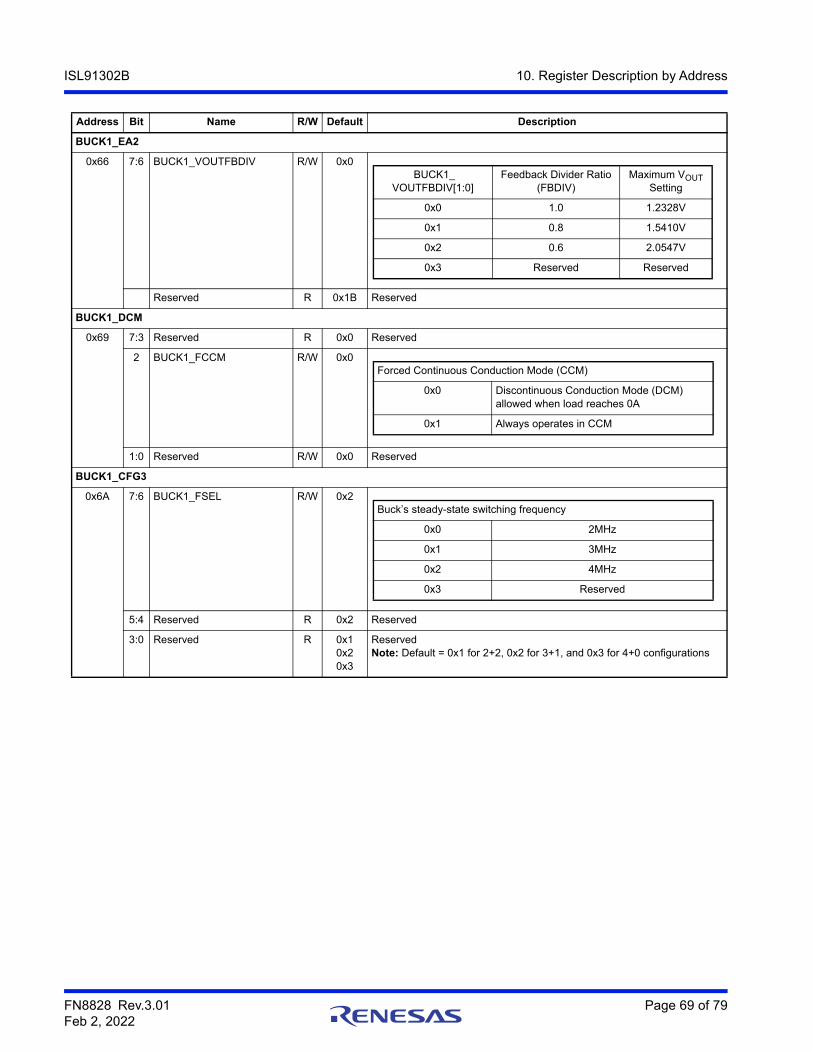
FN8828 Rev.3.01 Page 69 of 79Feb 2, 2022
ISL91302B 10. Register Description by Address
BUCK1_EA2
0x66 7:6 BUCK1_VOUTFBDIV R/W 0x0
Reserved R 0x1B Reserved
BUCK1_DCM
0x69 7:3 Reserved R 0x0 Reserved
2 BUCK1_FCCM R/W 0x0
1:0 Reserved R/W 0x0 Reserved
BUCK1_CFG3
0x6A 7:6 BUCK1_FSEL R/W 0x2
5:4 Reserved R 0x2 Reserved
3:0 Reserved R 0x10x20x3
ReservedNote: Default = 0x1 for 2+2, 0x2 for 3+1, and 0x3 for 4+0 configurations
Address Bit Name R/W Default Description
BUCK1_VOUTFBDIV[1:0]
Feedback Divider Ratio(FBDIV)
Maximum VOUT Setting
0x0 1.0 1.2328V
0x1 0.8 1.5410V
0x2 0.6 2.0547V
0x3 Reserved Reserved
Forced Continuous Conduction Mode (CCM)
0x0 Discontinuous Conduction Mode (DCM) allowed when load reaches 0A
0x1 Always operates in CCM
Buck’s steady-state switching frequency
0x0 2MHz
0x1 3MHz
0x2 4MHz
0x3 Reserved

FN8828 Rev.3.01 Page 70 of 79Feb 2, 2022
ISL91302B 10. Register Description by Address
BUCK1_PROTCFG
0x6E 7:4 Reserved R 0x0 Reserved
3 BUCK1_ENUVOV R/W 0x1
2 BUCK1_OVNOHYS R/W 0x1
1:0 BUCK1_UVOVTH R/W 0x2
BUCK1_DVS0CFG1
0x72 7:0 BUCK1_DVS0VOUT92 R/W Trim to 0.6V
Address Bit Name R/W Default Description
Undervoltage (UV) and Overvoltage (OV) comparators of VOUT
0x0 Disabled
0x1 EnabledNote: When the buck is programmed to 0V and the DAC[9:0] value reaches 0x000, the Overvoltage (OV) signal out of the buck is held low even though the buck output voltage may be higher than the Overvoltage (OV) threshold.
Hysteresis on the Overvoltage (OV) comparator of VOUT
0x0 Hysteresis enabled.OV flag goes low when VOUT decreases below the DAC target
0x1 Hysteresis disabled.OV flag goes low when VOUT goes below DAC target + offset (offset is set by BUCK1_UVOVTH[1:0]).
UV and OV trip thresholds of VOUT
0x0 ±150mV window around DAC target
0x1 ±200mV window around DAC target
0x2 ±250mV window around DAC target
0x3 ±300mV window around DAC target
Upper eight bits of a 10-bit DAC[9:0] value to generate VOUT for DVS Configuration 0.
Note: VOUT must be programmed above 0.3V.FBDIV is set by factory OTP to 1x, 0.8x, 0.6x. Refer to formula in (EQ. 1) on page 24.
FBDIV 1.0 0.8 0.6
DAC VOUT (V) VOUT (V) VOUT (V)
0x000 0.0000 0.0000 0.0000
0x001 0.0012 0.0015 0.0020
…
0x200 0.6170 0.7713 1.0283
0x201 0.6182 0.7728 1.0303
…
0x3E5 1.2015 1.5018 2.0024
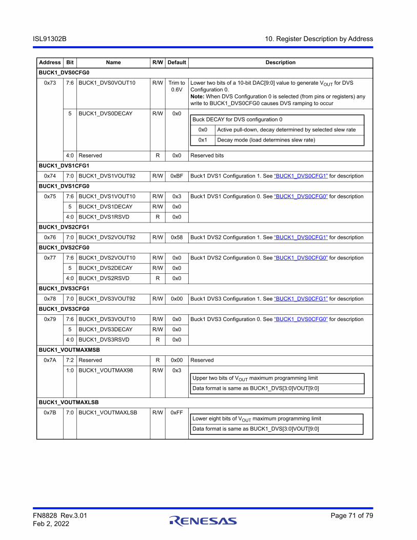
FN8828 Rev.3.01 Page 71 of 79Feb 2, 2022
ISL91302B 10. Register Description by Address
BUCK1_DVS0CFG0
0x73 7:6 BUCK1_DVS0VOUT10 R/W Trim to 0.6V
Lower two bits of a 10-bit DAC[9:0] value to generate VOUT for DVS Configuration 0.Note: When DVS Configuration 0 is selected (from pins or registers) any write to BUCK1_DVS0CFG0 causes DVS ramping to occur
5 BUCK1_DVS0DECAY R/W 0x0
4:0 Reserved R 0x0 Reserved bits
BUCK1_DVS1CFG1
0x74 7:0 BUCK1_DVS1VOUT92 R/W 0xBF Buck1 DVS1 Configuration 1. See “BUCK1_DVS0CFG1” for description
BUCK1_DVS1CFG0
0x75 7:6 BUCK1_DVS1VOUT10 R/W 0x3 Buck1 DVS1 Configuration 0. See “BUCK1_DVS0CFG0” for description
5 BUCK1_DVS1DECAY R/W 0x0
4:0 BUCK1_DVS1RSVD R 0x0
BUCK1_DVS2CFG1
0x76 7:0 BUCK1_DVS2VOUT92 R/W 0x58 Buck1 DVS2 Configuration 1. See “BUCK1_DVS0CFG1” for description
BUCK1_DVS2CFG0
0x77 7:6 BUCK1_DVS2VOUT10 R/W 0x0 Buck1 DVS2 Configuration 0. See “BUCK1_DVS0CFG0” for description
5 BUCK1_DVS2DECAY R/W 0x0
4:0 BUCK1_DVS2RSVD R 0x0
BUCK1_DVS3CFG1
0x78 7:0 BUCK1_DVS3VOUT92 R/W 0x00 Buck1 DVS3 Configuration 1. See “BUCK1_DVS0CFG1” for description
BUCK1_DVS3CFG0
0x79 7:6 BUCK1_DVS3VOUT10 R/W 0x0 Buck1 DVS3 Configuration 0. See “BUCK1_DVS0CFG0” for description
5 BUCK1_DVS3DECAY R/W 0x0
4:0 BUCK1_DVS3RSVD R 0x0
BUCK1_VOUTMAXMSB
0x7A 7:2 Reserved R 0x00 Reserved
1:0 BUCK1_VOUTMAX98 R/W 0x3
BUCK1_VOUTMAXLSB
0x7B 7:0 BUCK1_VOUTMAXLSB R/W 0xFF
Address Bit Name R/W Default Description
Buck DECAY for DVS configuration 0
0x0 Active pull-down, decay determined by selected slew rate
0x1 Decay mode (load determines slew rate)
Upper two bits of VOUT maximum programming limit
Data format is same as BUCK1_DVS[3:0]VOUT[9:0]
Lower eight bits of VOUT maximum programming limit
Data format is same as BUCK1_DVS[3:0]VOUT[9:0]

FN8828 Rev.3.01 Page 72 of 79Feb 2, 2022
ISL91302B 10. Register Description by Address
BUCK1_DVSCFG
0x7C 7:5 Reserved R 0x0 Reserved
4 BUCK1_PGOODDAC0V R/W 0x0
3:2 BUCK1_PGOODDELAY R/W 0x0
1:0 BUCK1_DVSPIN_CTRL R/W 0x0
See “Dynamic Voltage Scaling (DVS)” on page 23 for more information about using this register. This register is valid only in PINMODE 0x4 and OxE
Address Bit Name R/W Default Description
Power-Good state when Buck1 DAC is set to 0V
0x0 BUCK1_PGOOD is set low when the DAC is set to 0V
0x1 BUCK1_PGOOD is allowed to stay high when the DAC is set to 0V
Delay before the PGOOD signal is set (no delay when cleared)
Delay = BUCK1_PGOODDELAY[1:0] /32kHz (µs) Number of Clocks
0x0 0 0
0x1 125 4
0x2 375 12
0x3 1000 32
Register determines whether Buck1 follows global DVS pins
Bit<0>
0x0 BUCK1_DVSSELECT[0] does NOT follow DVS_PIN0.
0x1 BUCK1_DVSSELECT[0] mirrors DVS_PIN0.
Bit<1>
0x0 BUCK1_DVSSELECT[1] does NOT follow DVS_PIN1.
0x1 BUCK1_DVSSELECT[1] mirrors DVS_PIN1.
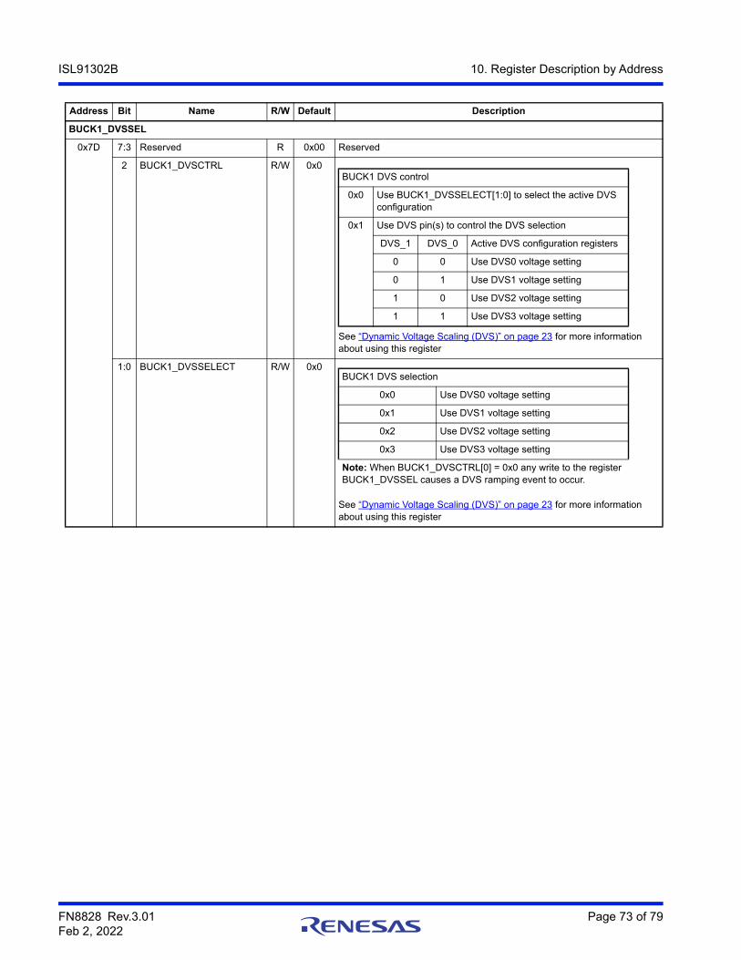
FN8828 Rev.3.01 Page 73 of 79Feb 2, 2022
ISL91302B 10. Register Description by Address
BUCK1_DVSSEL
0x7D 7:3 Reserved R 0x00 Reserved
2 BUCK1_DVSCTRL R/W 0x0
See “Dynamic Voltage Scaling (DVS)” on page 23 for more information about using this register
1:0 BUCK1_DVSSELECT R/W 0x0
See “Dynamic Voltage Scaling (DVS)” on page 23 for more information about using this register
Address Bit Name R/W Default Description
BUCK1 DVS control
0x0 Use BUCK1_DVSSELECT[1:0] to select the active DVS configuration
0x1 Use DVS pin(s) to control the DVS selection
DVS_1 DVS_0 Active DVS configuration registers
0 0 Use DVS0 voltage setting
0 1 Use DVS1 voltage setting
1 0 Use DVS2 voltage setting
1 1 Use DVS3 voltage setting
BUCK1 DVS selection
0x0 Use DVS0 voltage setting
0x1 Use DVS1 voltage setting
0x2 Use DVS2 voltage setting
0x3 Use DVS3 voltage setting
Note: When BUCK1_DVSCTRL[0] = 0x0 any write to the register BUCK1_DVSSEL causes a DVS ramping event to occur.

FN8828 Rev.3.01 Page 74 of 79Feb 2, 2022
ISL91302B 10. Register Description by Address
BUCK1_RSPCFG1
0x7E 7 BUCK1_RSPCFG1RSVD1 R 0x0 Reserved
6:4 BUCK1_RSPUP R/W 0x7 This slew rate is used when the current voltage is less than the target voltage.
3 Reserved R 0x0 Reserved
2:0 BUCK1_RSPDN R/W 0x3 This slew rate is used when the current voltage is greater than the target voltage.See BUCK1_RSPUP for decode information
Address Bit Name R/W Default Description
VOUT ramp slew rate.RSP = BUCK1_RSPUP[1:0], ramp speedFBDIV = BUCK1_VOUTFBDIV[1:0] = (1.0, 0.8, 0.6)Slow = BUCK1_RSPUP[2] = 0Fast = BUCK1_RSPUP[2] = 1
RSP FBDIV
VOUT Ramp Speed mV/µs
Fast Slow
0x0 1.0 12 3
0x1 1.0 24 6
0x2 1.0 57.6 14.4
0x3 1.0 115.2 28.8
RSP FBDIV
VOUT Ramp Speed mV/µs
Fast Slow
0x00x2
0.8/0.6 12 3
0x10x3
0.8/0.6 24 6
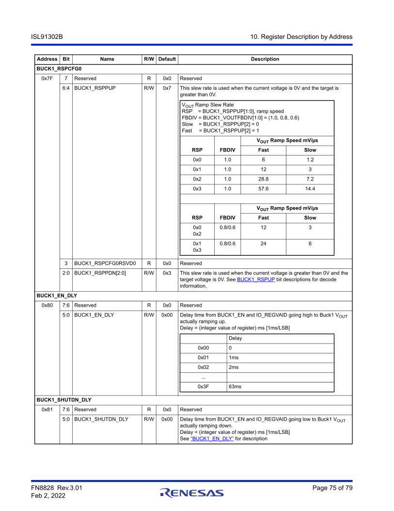
FN8828 Rev.3.01 Page 75 of 79Feb 2, 2022
ISL91302B 10. Register Description by Address
BUCK1_RSPCFG0
0x7F 7 Reserved R 0x0 Reserved
6:4 BUCK1_RSPPUP R/W 0x7 This slew rate is used when the current voltage is 0V and the target is greater than 0V.
3 BUCK1_RSPCFG0RSVD0 R 0x0 Reserved
2:0 BUCK1_RSPPDN[2:0] R/W 0x3 This slew rate is used when the current voltage is greater than 0V and the target voltage is 0V. See BUCK1_RSPUP bit descriptions for decode information.
BUCK1_EN_DLY
0x80 7:6 Reserved R 0x0 Reserved
5:0 BUCK1_EN_DLY R/W 0x00 Delay time from BUCK1_EN and IO_REGVAID going high to Buck1 VOUT actually ramping up.Delay = (integer value of register) ms [1ms/LSB]
BUCK1_SHUTDN_DLY
0x81 7:6 Reserved R 0x0 Reserved
5:0 BUCK1_SHUTDN_DLY R/W 0x00 Delay time from BUCK1_EN and IO_REGVAID going low to Buck1 VOUT actually ramping down.Delay = (integer value of register) ms [1ms/LSB]See “BUCK1_EN_DLY” for description
Address Bit Name R/W Default Description
VOUT Ramp Slew RateRSP = BUCK1_RSPPUP[1:0], ramp speedFBDIV = BUCK1_VOUTFBDIV[1:0] = (1.0, 0.8, 0.6)Slow = BUCK1_RSPPUP[2] = 0Fast = BUCK1_RSPPUP[2] = 1
RSP FBDIV
VOUT Ramp Speed mV/µs
Fast Slow
0x0 1.0 6 1.2
0x1 1.0 12 3
0x2 1.0 28.8 7.2
0x3 1.0 57.6 14.4
RSP FBDIV
VOUT Ramp Speed mV/µs
Fast Slow
0x00x2
0.8/0.6 12 3
0x10x3
0.8/0.6 24 6
Delay
0x00 0
0x01 1ms
0x02 2ms
...
0x3F 63ms
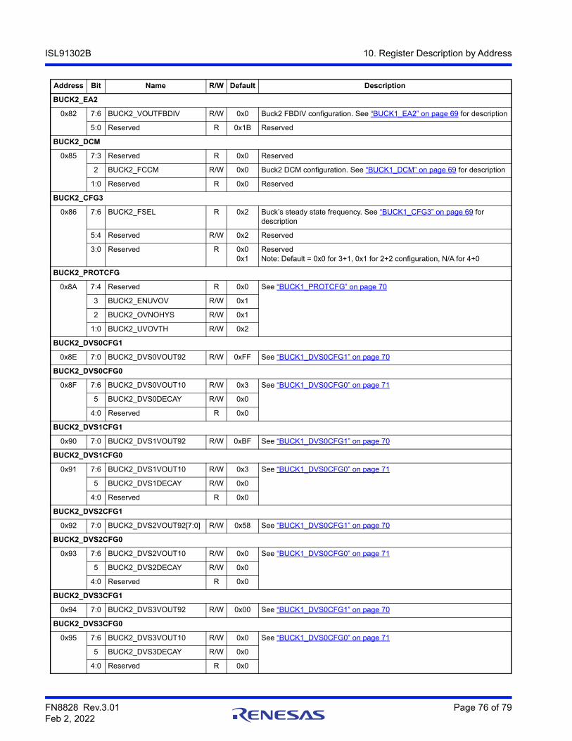
FN8828 Rev.3.01 Page 76 of 79Feb 2, 2022
ISL91302B 10. Register Description by Address
BUCK2_EA2
0x82 7:6 BUCK2_VOUTFBDIV R/W 0x0 Buck2 FBDIV configuration. See “BUCK1_EA2” on page 69 for description
5:0 Reserved R 0x1B Reserved
BUCK2_DCM
0x85 7:3 Reserved R 0x0 Reserved
2 BUCK2_FCCM R/W 0x0 Buck2 DCM configuration. See “BUCK1_DCM” on page 69 for description
1:0 Reserved R 0x0 Reserved
BUCK2_CFG3
0x86 7:6 BUCK2_FSEL R 0x2 Buck’s steady state frequency. See “BUCK1_CFG3” on page 69 for description
5:4 Reserved R/W 0x2 Reserved
3:0 Reserved R 0x00x1
ReservedNote: Default = 0x0 for 3+1, 0x1 for 2+2 configuration, N/A for 4+0
BUCK2_PROTCFG
0x8A 7:4 Reserved R 0x0 See “BUCK1_PROTCFG” on page 70
3 BUCK2_ENUVOV R/W 0x1
2 BUCK2_OVNOHYS R/W 0x1
1:0 BUCK2_UVOVTH R/W 0x2
BUCK2_DVS0CFG1
0x8E 7:0 BUCK2_DVS0VOUT92 R/W 0xFF See “BUCK1_DVS0CFG1” on page 70
BUCK2_DVS0CFG0
0x8F 7:6 BUCK2_DVS0VOUT10 R/W 0x3 See “BUCK1_DVS0CFG0” on page 71
5 BUCK2_DVS0DECAY R/W 0x0
4:0 Reserved R 0x0
BUCK2_DVS1CFG1
0x90 7:0 BUCK2_DVS1VOUT92 R/W 0xBF See “BUCK1_DVS0CFG1” on page 70
BUCK2_DVS1CFG0
0x91 7:6 BUCK2_DVS1VOUT10 R/W 0x3 See “BUCK1_DVS0CFG0” on page 71
5 BUCK2_DVS1DECAY R/W 0x0
4:0 Reserved R 0x0
BUCK2_DVS2CFG1
0x92 7:0 BUCK2_DVS2VOUT92[7:0] R/W 0x58 See “BUCK1_DVS0CFG1” on page 70
BUCK2_DVS2CFG0
0x93 7:6 BUCK2_DVS2VOUT10 R/W 0x0 See “BUCK1_DVS0CFG0” on page 71
5 BUCK2_DVS2DECAY R/W 0x0
4:0 Reserved R 0x0
BUCK2_DVS3CFG1
0x94 7:0 BUCK2_DVS3VOUT92 R/W 0x00 See “BUCK1_DVS0CFG1” on page 70
BUCK2_DVS3CFG0
0x95 7:6 BUCK2_DVS3VOUT10 R/W 0x0 See “BUCK1_DVS0CFG0” on page 71
5 BUCK2_DVS3DECAY R/W 0x0
4:0 Reserved R 0x0
Address Bit Name R/W Default Description
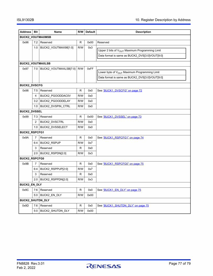
FN8828 Rev.3.01 Page 77 of 79Feb 2, 2022
ISL91302B 10. Register Description by Address
BUCK2_VOUTMAXMSB
0x96 7:2 Reserved R 0x00 Reserved
1:0 BUCK2_VOUTMAX98[1:0] R/W 0x3
BUCK2_VOUTMAXLSB
0x97 7:0 BUCK2_VOUTMAXLSB[7:0] R/W 0xFF
BUCK2_DVSCFG
0x98 7:5 Reserved R 0x0 See “BUCK1_DVSCFG” on page 72
4 BUCK2_PGOODDAC0V R/W 0x0
3:2 BUCK2_PGOODDELAY R/W 0x0
1:0 BUCK2_DVSPIN_CTRL R/W 0x0
BUCK2_DVSSEL
0x99 7:3 Reserved R 0x00 See “BUCK1_DVSSEL” on page 73
2 BUCK2_DVSCTRL R/W 0x0
1:0 BUCK2_DVSSELECT R/W 0x0
BUCK2_RSPCFG1
0x9A 7 Reserved R 0x0 See “BUCK1_RSPCFG1” on page 74
6:4 BUCK2_RSPUP R/W 0x7
3 Reserved R 0x0
2:0 BUCK2_RSPDN[2:0] R/W 0x3
BUCK2_RSPCFG0
0x9B 7 Reserved R 0x0 See “BUCK1_RSPCFG0” on page 75
6:4 BUCK2_RSPPUP[2:0] R/W 0x7
3 Reserved R 0x0
2:0 BUCK2_RSPPDN[2:0] R/W 0x3
BUCK2_EN_DLY
0x9C 7:6 Reserved R 0x0 See “BUCK1_EN_DLY” on page 75
5:0 BUCK2_EN_DLY R/W 0x00
BUCK2_SHUTDN_DLY
0x9D 7:6 Reserved R 0x0 See “BUCK1_SHUTDN_DLY” on page 75
5:0 BUCK2_SHUTDN_DLY R/W 0x00
Address Bit Name R/W Default Description
Upper 2 bits of VOUT Maximum Programming Limit
Data format is same as BUCK2_DVS[3:0]VOUT[9:0]
Lower byte of VOUT Maximum Programming Limit
Data format is same as BUCK2_DVS[3:0]VOUT[9:0]
FN8828 Rev.3.01 Page 78 of 79Feb 2, 2022
ISL91302B 11. Revision History
11. Revision History
Rev. Date Description
3.01 Feb 2, 2022 Removed Related Literature section.Updated Ordering Information table formatting.Updated Table 2 to show pinmode 0x2 and 0xF options, and mark as reserved.Clarify and correct temperature ratings and conditions in the Thermal Information, Recommended Operation Conditions, and Analog Specifications sections.Fixed incorrect IC part number in the Dynamic Voltage Scaling (DVS) and Power Sequencing sections.Added Eq.1 for 10-bit DAC to VOUT transfer function and removed Table 12.Updated and added numerous registers and details to Register Address Map and Register Description by Address sections.Added FBDIV settings to the description table for 0x66[7:6].Corrected Table of VOUT voltages in register 0x72.Updated ADC Telemetry section.
3.00 Feb 20, 2020 Updated Typical App Circuits.Added Note 1 to Ordering Information table.Updated Figure titles for Figures 16-11.Updated Figures 19, 20, 36, 38.Updated Table 12.Added the following sentence to section 7.1 on page 30: “The ISL91302B does not support SPI reads on the MISO bus when using multiple slave devices on the same bus.”Removed registers 0x78 (BUCK1_DVS3CFG1), and 0x82 (BUCK2EA2) and added registers 0x78 (BUCK2_DCM) and 0x86 (BUCK_CFG3) to Register Address Map on page 40.Added descriptions for registers BUCK1_DCM, BUCK1_CFG3, BUCK2_DCM, BUCK2_CFG3, ADC_BUCK1CFG, and ADC_BUCK2CFG to section 10, Register Descriptions.Updated disclaimer.
2.00 Apr 5, 2018 Updated Figures 3-5: INT (output) WDOG_RST (Input)Updated Note 2.Updated Parameter from “PVIN to GND” to “PVIN to PGND” on page 10.Updated the test condition for CCM Frequency Tolerance from 3MHz to 4MHz on page 12.Updated Figures 24 and 26.
1.00 Feb 28, 2018 Updated TitleUpdated Figure 1Added Table 1 on page 6.Updated the Analog Specifications Conditions in table heading.Added Buck Output Voltage Range, and Output Voltage Step Size for BUCKx_VOUTFBDIV[1:0] = 0x00, BUCKx_VOUTFBDIV[1:0] = 0x01, BUCKx_VOUTFBDIV[1:0] = 0x02 in Spec table on page 11.Added High-Side and Low-Side Switch On-Resistance specs on page 12.Updated Table 5.Updated Figure 30.Updated Data Hold Time minimum specifications for all modes in Table 18 on page 35 (changed from 0ns to 15ns).Updated IO_CHIPNAME description on page 41.Updated FLT_RECORDBUCK2 Bits 1, 3, 5 names on page 44.Added Default information for FLT_OT_CTRL on page 61 and BUCK1_RSPCFG1 on page 67.Updated description for BUCK1_DVS0CFG1 on page 64 (changed 0.4V to 0.3V).Removed About Intersil section.Updated disclaimer.
0.00 Sep 22, 2017 Initial release
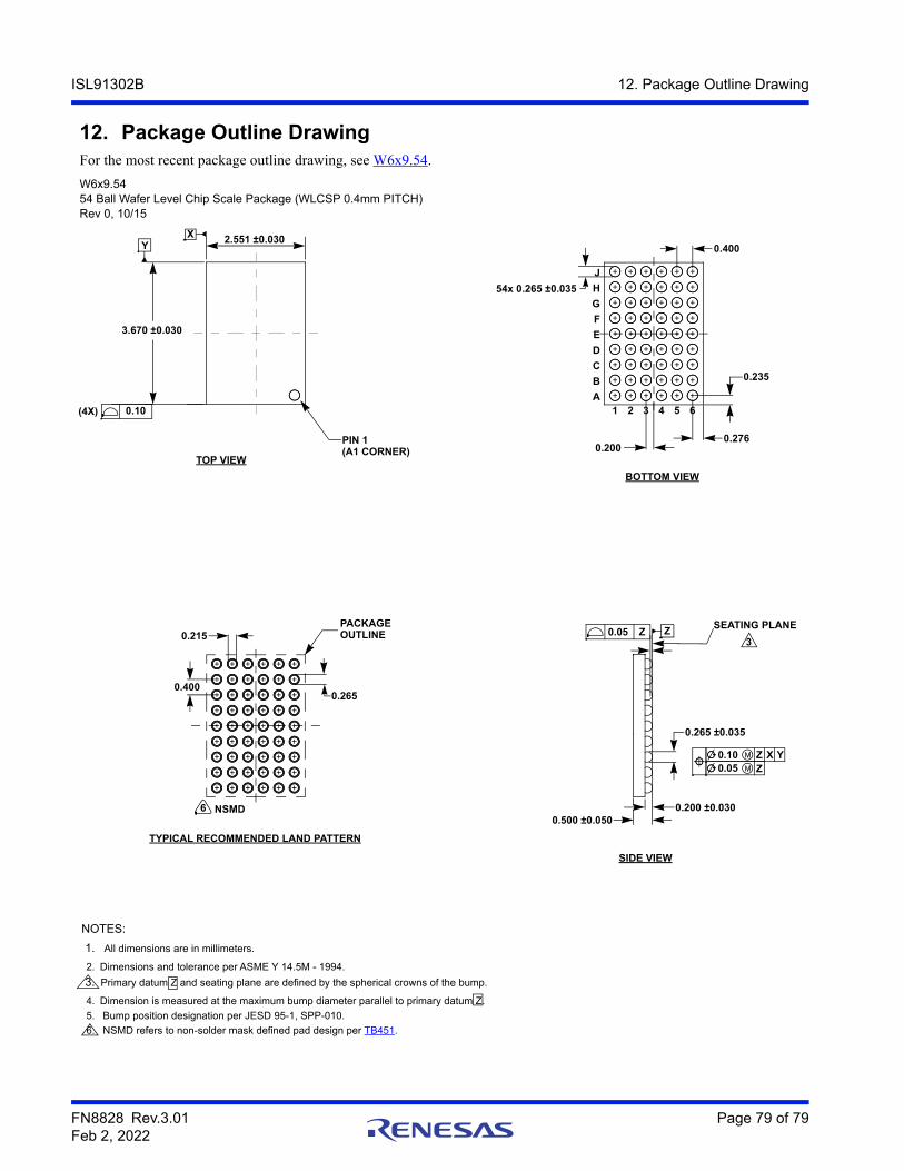
FN8828 Rev.3.01 Page 79 of 79Feb 2, 2022
ISL91302B 12. Package Outline Drawing
12. Package Outline DrawingFor the most recent package outline drawing, see W6x9.54.
W6x9.5454 Ball Wafer Level Chip Scale Package (WLCSP 0.4mm PITCH) Rev 0, 10/15
NOTES:
1. All dimensions are in millimeters.
2. Dimensions and tolerance per ASME Y 14.5M - 1994.
3. Primary datum Z and seating plane are defined by the spherical crowns of the bump.
4. Dimension is measured at the maximum bump diameter parallel to primary datum Z.
5. Bump position designation per JESD 95-1, SPP-010.
6. NSMD refers to non-solder mask defined pad design per TB451.
BOTTOM VIEW
SIDE VIEW
TYPICAL RECOMMENDED LAND PATTERN
TOP VIEW
Z0.05 Z
0.10 Z X Y0.05 Z
PACKAGE SEATING PLANE
0.265 ±0.035
OUTLINE
0.265
0.200 ±0.030
3
0.500 ±0.050
5431 2 6
2.551 ±0.030Y
X
3.670 ±0.030
0.10(4X)
PIN 1 (A1 CORNER)
0.400
54x 0.265 ±0.035
0.235
0.2760.200
A
B
C
D
E
F
G
H
J
0.400
0.215
NSMD6
Corporate HeadquartersTOYOSU FORESIA, 3-2-24 Toyosu,Koto-ku, Tokyo 135-0061, Japanwww.renesas.com
Contact InformationFor further information on a product, technology, the most up-to-date version of a document, or your nearest sales office, please visit:www.renesas.com/contact/
TrademarksRenesas and the Renesas logo are trademarks of Renesas Electronics Corporation. All trademarks and registered trademarks are the property of their respective owners.
IMPORTANT NOTICE AND DISCLAIMER
RENESAS ELECTRONICS CORPORATION AND ITS SUBSIDIARIES (“RENESAS”) PROVIDES TECHNICAL SPECIFICATIONS AND RELIABILITY DATA (INCLUDING DATASHEETS), DESIGN RESOURCES (INCLUDING REFERENCE DESIGNS), APPLICATION OR OTHER DESIGN ADVICE, WEB TOOLS, SAFETY INFORMATION, AND OTHER RESOURCES “AS IS” AND WITH ALL FAULTS, AND DISCLAIMS ALL WARRANTIES, EXPRESS OR IMPLIED, INCLUDING, WITHOUT LIMITATION, ANY IMPLIED WARRANTIES OF MERCHANTABILITY, FITNESS FOR A PARTICULAR PURPOSE, OR NON-INFRINGEMENT OF THIRD PARTY INTELLECTUAL PROPERTY RIGHTS.
These resources are intended for developers skilled in the art designing with Renesas products. You are solely responsible for (1) selecting the appropriate products for your application, (2) designing, validating, and testing your application, and (3) ensuring your application meets applicable standards, and any other safety, security, or other requirements. These resources are subject to change without notice. Renesas grants you permission to use these resources only for development of an application that uses Renesas products. Other reproduction or use of these resources is strictly prohibited. No license is granted to any other Renesas intellectual property or to any third party intellectual property. Renesas disclaims responsibility for, and you will fully indemnify Renesas and its representatives against, any claims, damages, costs, losses, or liabilities arising out of your use of these resources. Renesas' products are provided only subject to Renesas' Terms and Conditions of Sale or other applicable terms agreed to in writing. No use of any Renesas resources expands or otherwise alters any applicable warranties or warranty disclaimers for these products.
(Rev.1.0 Mar 2020)


