etsi en 301 841-1 v1.4 · etsi 6 etsi en 301 841-1 v1.4.1 (2015-04) intellectual property rights...
TRANSCRIPT
ETSI EN 301 841-1 V1.4.1 (2015-04)
VHF air-ground Digital Link (VDL) Mode 2; Technical characteristics and
methods of measurement for ground-based equipment;
Part 1: Physical layer and MAC sub-layer
EUROPEAN STANDARD

ETSI
ETSI EN 301 841-1 V1.4.1 (2015-04) 2
Reference REN/AERO-00010
Keywords aeronautical, radio, testing, VHF
ETSI
650 Route des Lucioles F-06921 Sophia Antipolis Cedex - FRANCE
Tel.: +33 4 92 94 42 00 Fax: +33 4 93 65 47 16
Siret N° 348 623 562 00017 - NAF 742 C
Association à but non lucratif enregistrée à la Sous-Préfecture de Grasse (06) N° 7803/88
Important notice
The present document can be downloaded from: http://www.etsi.org/standards-search
The present document may be made available in electronic versions and/or in print. The content of any electronic and/or print versions of the present document shall not be modified without the prior written authorization of ETSI. In case of any
existing or perceived difference in contents between such versions and/or in print, the only prevailing document is the print of the Portable Document Format (PDF) version kept on a specific network drive within ETSI Secretariat.
Users of the present document should be aware that the document may be subject to revision or change of status. Information on the current status of this and other ETSI documents is available at
http://portal.etsi.org/tb/status/status.asp
If you find errors in the present document, please send your comment to one of the following services: https://portal.etsi.org/People/CommiteeSupportStaff.aspx
Copyright Notification
No part may be reproduced or utilized in any form or by any means, electronic or mechanical, including photocopying and microfilm except as authorized by written permission of ETSI.
The content of the PDF version shall not be modified without the written authorization of ETSI. The copyright and the foregoing restriction extend to reproduction in all media.
© European Telecommunications Standards Institute 2015.
All rights reserved.
DECTTM, PLUGTESTSTM, UMTSTM and the ETSI logo are Trade Marks of ETSI registered for the benefit of its Members. 3GPPTM and LTE™ are Trade Marks of ETSI registered for the benefit of its Members and
of the 3GPP Organizational Partners. GSM® and the GSM logo are Trade Marks registered and owned by the GSM Association.
ETSI
ETSI EN 301 841-1 V1.4.1 (2015-04) 3
Contents Intellectual Property Rights ................................................................................................................................ 6
Foreword ............................................................................................................................................................. 6
Modal verbs terminology .................................................................................................................................... 6
Introduction ........................................................................................................................................................ 6
1 Scope ........................................................................................................................................................ 7
2 References ................................................................................................................................................ 7
2.1 Normative references ......................................................................................................................................... 7
2.2 Informative references ........................................................................................................................................ 7
3 Definitions and abbreviations ................................................................................................................... 8
3.1 Definitions .......................................................................................................................................................... 8
3.1.1 Basic reference model definitions ................................................................................................................. 8
3.1.2 Service conventions definitions .................................................................................................................... 8
3.1.3 General definitions ........................................................................................................................................ 9
3.2 Abbreviations ..................................................................................................................................................... 9
4 General architecture of VDL Mode 2 ..................................................................................................... 10
5 Physical layer protocols and services functional specifications ............................................................. 11
5.1 Overview .......................................................................................................................................................... 11
5.1.1 Functions .................................................................................................................................................... 11
5.1.2 Data reception by the receiver .................................................................................................................... 12
5.1.3 Data transmission ........................................................................................................................................ 12
5.2 Transmission procedure ................................................................................................................................... 12
5.3 Modulation scheme .......................................................................................................................................... 13
5.4 Training sequence............................................................................................................................................. 13
5.4.1 RF power rise time definition ..................................................................................................................... 13
5.5 Physical layer Service Access Point ................................................................................................................. 14
5.6 Tuning range and channel increments .............................................................................................................. 14
6 VDL MODE 2 equipment requirements ................................................................................................ 14
6.1 Transmitter requirements ................................................................................................................................. 14
6.1.1 Frequency Tolerance................................................................................................................................... 14
6.1.2 Manufacturer's declared output power ........................................................................................................ 14
6.1.3 Adjacent channel power .............................................................................................................................. 15
6.1.3.1 16 kHz channel bandwidth .................................................................................................................... 15
6.1.3.2 25 kHz channel bandwidth .................................................................................................................... 15
6.1.4 Conducted Spurious emissions ................................................................................................................... 16
6.1.5 Cabinet radiation ......................................................................................................................................... 16
6.1.6 Modulation rate ........................................................................................................................................... 16
6.1.7 Intermodulation attenuation ........................................................................................................................ 16
6.1.8 RF power rise time ...................................................................................................................................... 16
6.1.9 RF power release time ................................................................................................................................ 16
6.1.10 Transceiver timing requirements ................................................................................................................ 17
6.1.10.1 Receiver to transmitter turn-around time .............................................................................................. 17
6.1.10.2 Transmitter to receiver turn-around time .............................................................................................. 17
6.1.11 Symbol constellation error .......................................................................................................................... 17
6.1.12 Protection of the transmitter........................................................................................................................ 17
6.1.13 Load VSWR capability ............................................................................................................................... 17
6.2 Receiver requirements ...................................................................................................................................... 17
6.2.1 Sensitivity ................................................................................................................................................... 17
6.2.2 Co-channel interference .............................................................................................................................. 17
6.2.3 First Adjacent Channel Rejection ............................................................................................................... 17
6.2.4 Rejection of signals within the VHF Aeronautical band............................................................................. 18
6.2.5 Rejection of signals outside the VHF Aeronautical band ........................................................................... 18
6.2.6 In-band Intermodulation ............................................................................................................................. 18
6.2.7 Desired signal dynamic range ..................................................................................................................... 19

ETSI
ETSI EN 301 841-1 V1.4.1 (2015-04) 4
6.2.8 Conducted spurious emission ..................................................................................................................... 19
6.2.9 Cabinet radiation ......................................................................................................................................... 19
6.2.10 Symbol rate capture range .......................................................................................................................... 19
6.2.11 Frequency capture range ............................................................................................................................. 19
6.3 Void .................................................................................................................................................................. 19
6.4 MAC sub-layer requirements ........................................................................................................................... 19
6.4.1 MAC services ............................................................................................................................................. 19
6.4.1.1 Multiple Access ..................................................................................................................................... 19
6.4.1.2 Channel Congestion .............................................................................................................................. 19
6.4.2 MAC System Parameters ............................................................................................................................ 19
6.4.2.1 Timer TM1 (inter-access delay timer)................................................................................................... 19
6.4.2.2 Timer TM2 (channel busy timer) .......................................................................................................... 20
6.4.2.3 Parameter p (persistence) ...................................................................................................................... 20
6.4.2.4 Counter M1 (maximum access attempts) .............................................................................................. 20
6.4.3 Description of MAC Layer Procedures ...................................................................................................... 20
6.4.3.1 Channel Sensing .................................................................................................................................... 20
6.4.3.2 Access Attempt ..................................................................................................................................... 20
6.4.3.3 Signal Quality Parameter ...................................................................................................................... 20
6.4.4 Services (Part of DLS) ................................................................................................................................ 20
6.4.4.1 Error Detection ...................................................................................................................................... 20
6.4.4.2 Station Identification ............................................................................................................................. 20
7 General requirements ............................................................................................................................. 21
7.1 General ............................................................................................................................................................. 21
7.2 Controls and indicators ..................................................................................................................................... 21
7.3 Class of emission and modulation characteristics ............................................................................................ 21
7.4 Warm up ........................................................................................................................................................... 21
8 Test conditions, power sources and ambient temperatures .................................................................... 21
8.1 Test power source ............................................................................................................................................. 21
8.2 Normal and extreme test conditions ................................................................................................................. 21
8.2.1 Normal test conditions ................................................................................................................................ 21
8.2.1.1 Normal temperature and humidity ........................................................................................................ 21
8.2.1.2 Normal power sources ........................................................................................................................... 22
8.2.1.2.1 Mains voltage and frequency ........................................................................................................... 22
8.2.1.2.2 Other power sources ........................................................................................................................ 22
8.2.2 Extreme test conditions ............................................................................................................................... 22
8.2.2.1 Extreme temperatures ............................................................................................................................ 22
8.2.2.2 Procedure for tests at extreme temperatures .......................................................................................... 22
8.2.2.2.1 General ............................................................................................................................................ 22
8.2.2.2.2 High temperature ............................................................................................................................. 22
8.2.2.2.3 Low temperature .............................................................................................................................. 22
8.2.2.3 Extreme values of test power sources ................................................................................................... 23
8.2.2.4 Other power sources .............................................................................................................................. 23
8.3 Test channels .................................................................................................................................................... 23
8.4 General conditions of measurement ................................................................................................................. 23
8.4.1 Receiver test signal arrangement ................................................................................................................ 23
8.4.2 Receiver BER test ....................................................................................................................................... 23
8.4.3 Performance check ...................................................................................................................................... 24
9 Detailed Test Procedures for the physical layer ..................................................................................... 25
9.1 Transmitter ....................................................................................................................................................... 25
9.1.1 Frequency Error .......................................................................................................................................... 25
9.1.1.1 Definition .............................................................................................................................................. 25
9.1.1.2 Method of measurement ........................................................................................................................ 25
9.1.1.3 Limits .................................................................................................................................................... 25
9.1.2 Manufacturer's declared output power ........................................................................................................ 25
9.1.3 Adjacent channel power .............................................................................................................................. 26
9.1.3.1 Method of measurement for the first adjacent channel ......................................................................... 26
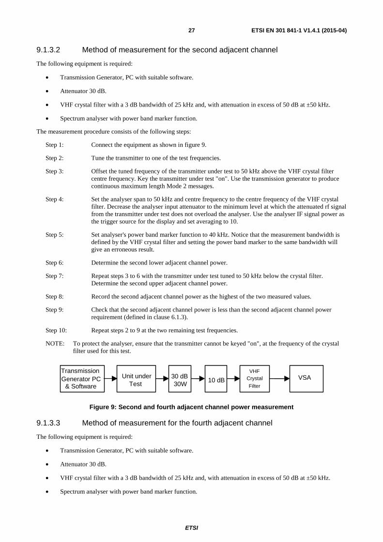
9.1.3.2 Method of measurement for the second adjacent channel ..................................................................... 27
9.1.3.3 Method of measurement for the fourth adjacent channel ...................................................................... 27
9.1.3.4 Wideband noise ..................................................................................................................................... 29
9.1.4 Spurious emissions ..................................................................................................................................... 30

ETSI
ETSI EN 301 841-1 V1.4.1 (2015-04) 5
9.1.5 Cabinet Radiation ....................................................................................................................................... 30
9.1.6 Void ............................................................................................................................................................ 30
9.1.7 Inter-modulation attenuation ....................................................................................................................... 30
9.1.8 RF power rise time ...................................................................................................................................... 31
9.1.9 RF power release time ................................................................................................................................ 33
9.1.10 Physical layer, system parameters .............................................................................................................. 34
9.1.10.1 Receiver to Transmitter turn-around time ............................................................................................. 34
9.1.10.2 Transmitter to Receiver turn-around time ............................................................................................. 35
9.1.11 Symbol Constellation Error ........................................................................................................................ 36
9.1.12 Protection of the transmitter........................................................................................................................ 37
9.1.12.1 Method of measurement ........................................................................................................................ 37
9.1.12.2 Requirement .......................................................................................................................................... 37
9.1.13 Load VSWR capability ............................................................................................................................... 37
9.2 Receiver ............................................................................................................................................................ 38
9.2.1 Sensitivity ................................................................................................................................................... 38
9.2.2 Co-channel interference .............................................................................................................................. 38
9.2.3 First Adjacent Channel Rejection ............................................................................................................... 39
9.2.4 Rejection of signals within the VHF Aeronautical band............................................................................. 40
9.2.5 Rejection of signals outside the VHF Aeronautical band ........................................................................... 41
9.2.6 In-band Intermodulation ............................................................................................................................. 41
9.2.7 Desired Signal dynamic range .................................................................................................................... 42
9.2.8 Conducted spurious emission ..................................................................................................................... 43
9.2.9 Cabinet Radiation ....................................................................................................................................... 43
9.2.10 Symbol rate capture range .......................................................................................................................... 43
9.2.11 Frequency capture range ............................................................................................................................. 44
9.3 Void .................................................................................................................................................................. 44
9.4 MAC sub-layer ................................................................................................................................................. 44
9.4.1 MAC services ............................................................................................................................................. 45
9.4.1.1 Multiple Access ..................................................................................................................................... 45
9.4.1.2 Channel Congestion .............................................................................................................................. 45
9.4.2 MAC System Parameters ............................................................................................................................ 45
9.4.2.1 Timer TM1 (inter-access delay timer)................................................................................................... 45
9.4.2.2 Timer TM2 (channel busy timer) .......................................................................................................... 46
9.4.2.3 Parameter p (persistence) ...................................................................................................................... 46
9.4.2.4 Counter M1 (maximum access attempts) .............................................................................................. 47
9.4.3 Description of MAC Layer Procedures ...................................................................................................... 48
9.4.3.1 Channel Sensing .................................................................................................................................... 48
9.4.3.2 Access Attempt ..................................................................................................................................... 48
9.4.3.3 Signal Quality Parameter ...................................................................................................................... 49
9.4.4 Services (Part of DLS) ................................................................................................................................ 49
9.4.4.1 Error Detection ...................................................................................................................................... 49
9.4.4.2 Station Identification ............................................................................................................................. 50
Annex A (informative): Bibliography ........................................................................................................... 51
History .............................................................................................................................................................. 52

ETSI
ETSI EN 301 841-1 V1.4.1 (2015-04) 6
Intellectual Property Rights IPRs essential or potentially essential to the present document may have been declared to ETSI. The information pertaining to these essential IPRs, if any, is publicly available for ETSI members and non-members, and can be found in ETSI SR 000 314: "Intellectual Property Rights (IPRs); Essential, or potentially Essential, IPRs notified to ETSI in respect of ETSI standards", which is available from the ETSI Secretariat. Latest updates are available on the ETSI Web server (http://ipr.etsi.org).
Pursuant to the ETSI IPR Policy, no investigation, including IPR searches, has been carried out by ETSI. No guarantee can be given as to the existence of other IPRs not referenced in ETSI SR 000 314 (or the updates on the ETSI Web server) which are, or may be, or may become, essential to the present document.
Foreword This European Standard (EN) has been produced by ETSI Technical Committee Aeronautics (AERO).
The present document is part 1 of a multi-part deliverable covering VHF air-ground Digital Link (VDL) Mode 2; Technical characteristics and methods of measurement for ground-based equipment, as identified below:
Part 1: "Physical layer and MAC sub-layer";
Part 2: "Upper layers";
Part 3: "Harmonized EN covering the essential requirements of article 3.2 of the R&TTE Directive".
National transposition dates
Date of adoption of this EN: 21 April 2015
Date of latest announcement of this EN (doa): 31 July 2015
Date of latest publication of new National Standard or endorsement of this EN (dop/e):
31 January 2016
Date of withdrawal of any conflicting National Standard (dow): 31 January 2016
Modal verbs terminology In the present document "shall", "shall not", "should", "should not", "may", "need not", "will", "will not", "can" and "cannot" are to be interpreted as described in clause 3.2 of the ETSI Drafting Rules (Verbal forms for the expression of provisions).
"must" and "must not" are NOT allowed in ETSI deliverables except when used in direct citation.
Introduction The present document states the technical specifications for ground-based equipment implementing Very High Frequency (VHF) Digital Link (VDL) Mode 2 air interface, operating in the VHF band (117,975 MHz to 137,000 MHz) with 25 kHz channel spacing.
Manufacturers should note that in the future, all or part of the frequency band 108,000 MHz to 117,975 MHz may become available for aeronautical communications.
The VDL Mode 2 system is designed to be a Ground/Air sub-system of the Aeronautical Telecommunication Network (ATN) using the AM(R)S band and it is organized according to the Open Systems Interconnection (OSI) model (defined by ISO). It will provide reliable subnetwork services to the ATN system.
The present document may be used to produce tests for the assessment of the performance of the equipment.

ETSI
ETSI EN 301 841-1 V1.4.1 (2015-04) 7
1 Scope The present document applies to VDL Mode 2 ground-air digital communications using Differential Eight Phase Shift Keying (D8PSK), intended for channel increments of 25 kHz. The VDL Mode 2 system provides data communication exchanges between aircraft and ground-based systems. The scope of the present document is limited to ground-based stations.
The present document provides functional specifications for ground-based radio equipment intended to be used for ground-air data communications. The present document is derived from the following documents:
• Annex 10 of the ICAO Convention on International Civil Aviation [1].
• ED 92B [i.2]: "MOPS for an Airborne VDL Mode-2 Transceiver Operating in the frequency range 118-136.975 MHz" (2012), which specifies the airborne transceiver.
The present document consists of two parts:
• the first part provides functional specifications and test procedures for physical layer and MAC sub-layer;
• the second part provides functional specifications and test procedures for link and sub-network access layers.
2 References
2.1 Normative references References are either specific (identified by date of publication and/or edition number or version number) or non-specific. For specific references, only the cited version applies. For non-specific references, the latest version of the reference document (including any amendments) applies.
Referenced documents which are not found to be publicly available in the expected location might be found at http://docbox.etsi.org/Reference.
NOTE: While any hyperlinks included in this clause were valid at the time of publication ETSI cannot guarantee their long term validity.
The following referenced documents are necessary for the application of the present document.
[1] ICAO Convention on International Civil Aviation: "Annex 10 - Aeronautical Telecommunications, Volume III - Communication Systems, Part I - Digital Data Communication Systems, Second Edition, July 2007, incorporating Amendments up to 88A (applicable 14/11/13). Chapter 6 - VHF Air-ground Digital Link (VDL)".
[2] ICAO Convention on International Civil Aviation: "Annex 10 - Aeronautical Telecommunications, Volume V - Aeronautical Radio Frequency Spectrum Utilization", Third Edition, July 2013 incorporating Amendments up to 88A.
[3] ETSI EN 300 113-1: "Electromagnetic compatibility and Radio spectrum Matters (ERM); Land mobile service; Radio equipment intended for the transmission of data (and/or speech) using constant or non-constant envelope modulation and having an antenna connector; Part 1: Technical characteristics and methods of measurement".
[4] ICAO Document 9776/AN970 (first edition, 2001): "Manual on VHF Digital Link (VDL) mode 2".
2.2 Informative references References are either specific (identified by date of publication and/or edition number or version number) or non-specific. For specific references, only the cited version applies. For non-specific references, the latest version of the reference document (including any amendments) applies.
NOTE: While any hyperlinks included in this clause were valid at the time of publication ETSI cannot guarantee their long term validity.

ETSI
ETSI EN 301 841-1 V1.4.1 (2015-04) 8
The following referenced documents are not necessary for the application of the present document but they assist the user with regard to a particular subject area.
[i.1] ETSI EN 301 841-2: "Electromagnetic compatibility and Radio spectrum Matters (ERM); VHF air-ground Digital Link (VDL) Mode 2; Technical characteristics and methods of measurement for ground-based equipment; Part 2: Upper layers".
[i.2] EUROCAE ED 92B: "MOPS for an Airborne VDL Mode-2 Transceiver operating in the frequency range 118-136.975 MHz".
[i.3] ISO/IEC 13239: "Information technology - Telecommunications and information exchange between systems - High-level data link control (HDLC) procedures".
[i.4] ISO/IEC 8208: "Information technology - Data communications - X.25 Packet Layer Protocol for Data Terminal Equipment".
[i.5] ISO/IEC 7498-1: "Information technology - Open Systems Interconnection - Basic Reference Model: The Basic Model".
[i.6] ISO/IEC 10731: "Information technology - Open Systems Interconnection - Basic Reference Model - Conventions for the definition of OSI services".
[i.7] ITU Radio Regulations (2012).
3 Definitions and abbreviations
3.1 Definitions
3.1.1 Basic reference model definitions
The present document is based on the concepts developed in the open systems interconnect basic reference model and makes use of the following terms defined in ISO/IEC 7498-1 [i.5]:
• layer;
• sublayer;
• entity;
• service;
• service access point;
• service data unit;
• physical layer;
• data link layer.
3.1.2 Service conventions definitions
For the purposes of the present document, the terms and definitions given in ISO/IEC 10731 [i.6] apply:
• service provider;
• service user;
• service primitive;
• request;
• indication;
• confirm.
ETSI
ETSI EN 301 841-1 V1.4.1 (2015-04) 9
3.1.3 General definitions
For the purposes of the present document, the following terms and definitions apply:
adjacent channel power: amount of the modulated RF signal power transmitted outside of the assigned channel
NOTE: Adjacent channel power includes discrete spurious, signal sidebands, and noise density (including phase noise) at the transmitter output.
adjacent channel rejection: receiver's ability to demodulate the desired signal and meet the uncorrected BER requirement in the presence of an interfering signal in an adjacent channel
NOTE: The ratio (in dB) between the adjacent interfering signal level and the desired signal level necessary to achieve the specified minimum uncorrected BER, is the adjacent channel rejection (ACR) ratio.
aeronautical mobile service: mobile service between aeronautical stations and aircraft stations, or between aircraft stations, in which survival craft stations may participate
average transmitter output power: average power supplied to the antenna transmission line by a transmitter during an interval of time sufficiently long, compared with the lowest frequency encountered in the modulation, taken under normal operating conditions
Bit Error Rate (BER): ratio between the number of erroneous bits received and the total number of bits received
NOTE: The uncorrected BER represents the BER without the benefit of Forward Error Correction (FEC).
Co-Channel Interference (CCI): capability of a receiver to demodulate the desired signal and achieve the minimum specified BER performance in the presence of an unwanted signal at the same assigned channel
NOTE: The ratio (in dB) between the wanted signal level and the unwanted signal level is the co-channel interference ratio.
conducted measurements: measurements which are made using a direct rf connection to the equipment under test
ground base station: aeronautical station equipment, in the aeronautical mobile service, for use with an external antenna and intended for use at a fixed location
spurious emissions: conducted rf emissions on a frequency or frequencies which are outside the necessary bandwidth and the level of which may be reduced without affecting the corresponding transmission of information
NOTE: Spurious emissions include parasitic emissions, intermodulation products and frequency conversion products.
X 25: ITU-T standard for the protocols and message formats that define the interface between a terminal and a packet switching network
3.2 Abbreviations For the purposes of the present document, the following abbreviations apply:
AC Alternating Current ACP Adjacent Channel Protection ACR Adjacent Channel Rejection AGC Automatic Gain Control AM(R)S Aeronautical Mobile (Route) Service ATN Aeronautical Telecommunication Network AVL Aviation VHF Link AVLC Aviation VHF Link Control AVLC_LI Aviation VHF Link Control Length Indicator AVPL Aviation VHF Physical Layer AVPL-Header AVPL Header and training sequence AVPL-TBS AVPL Transmitted Bit Scrambled sequence AVPL-THeader AVPL Transmission Header sequence AVPL-THI AVPL Transmitted Header appended and Interleaved sequence AVPL-TIRS AVPL Transmitted Interleaved RS encoded sequence

ETSI
ETSI EN 301 841-1 V1.4.1 (2015-04) 10
AVPL-TTS AVPL Transmitted Ternary Symbol sequence AWG Arbitrary Waveform Generator BER Bit Error Rate CCI Co Channel Interference CRC Cyclic Redundancy Check CSMA Carrier Sense Multiple Access CW Continuous Wave D8PSK Differentially encoded 8 Phase Shift Keying dBc Decibels relative to the carrier dBm Decibels relative to 1 milliwatt DLS Data Link Service ED Eurocae Document EVM Error Vector Magnitude FCS Frame Check Sequence FEC Forward Error Correction FM Frequency Modulation HDLC High-level Data Link Control ICAO International Civil Aviation Organization IF Intermediate Frequency ISO International Organization for Standardization LME Link Management Entity MAC Media Access Control MOPS Minimum Operational Performance Specification OSI Open Systems Interconnection PC Personal Computer ppm parts per million RF Radio Frequency RMS Root Mean Square RS Reed-Solomon RSSI Received Signal Strength Indicator SAP Service Access Point SARPS Standards And Recommended PracticeS (ICAO) SNAcP SubNetwork Access Protocol SQP Signal Quality Parameter TIRS matrix Transmission Interleaver and RS encoding matrix VDL VHF Digital Link VHF Very High Frequency VME VDL Management Entity VSA Vector Signal Analyser VSWR Voltage Standing Wave Radio
4 General architecture of VDL Mode 2 The general architecture of the VHF radio equipment operating in VDL Mode 2 is depicted in figure 1. This figure presents the different functional parts of the VDL Mode 2 equipment.
The VDL system is related to the three lower layers of the OSI model providing services described as follows:
Layer 1 (Physical layer): provides transceiver frequency control, bit exchanges over the radio media, and notification functions. These functions are often known as radio and modulation functions. The physical layer handles information exchanges at the lowest level and manipulates bits. The physical layer handles modulation, data encoding and includes a forward error correction mechanism based on interleaving and Reed Solomon coding.
Layer 2 (Link Layer): is split into two sublayers and a link management entity:
• The MAC sublayer provides access to the Physical layer by a CSMA algorithm in charge of channel access. The MAC layer controls channel access and sharing.
• The DLS sublayer is composed of the AVLC derived from the HDLC protocol (ISO/IEC 13239 [i.3]) whose main functions are frame exchanges, frame processing, and error detection.
• The LME controls the link establishment and maintenance between DLS sublayers.

ETSI
ETSI EN 301 841-1 V1.4.1 (2015-04) 11
Layer 3: Only the lowest network sublayer of layer 3 (SNAcP) will be described in ETSI EN 301 841-2 [i.1]. It is compliant with the subnetwork sublayer requirements defined in the ATN SARPs and conforms with the ISO/IEC 8208 [i.4] (or network layer of X.25). It provides packet exchanges over a virtual circuit, error recovery, connection flow control, packet fragmentation, and subnetwork connection management functions.
The DLS and LME part of the Layer 2 and Layer 3 are specified in ETSI EN 301 841-2 [i.1].
D8PSK (31,5 kbits/s)
DLS (AVLC)
MAC (CSMA)
LME
INTERNETWORKSUBLAYER
TRANSPORT LAYER
SESSION LAYER
PRESENTATIONLAYER
APPLICATIONLAYER
VDL MODE 2 SARPs
: ATN SARPs
Layer 1
Layer 2
Layer 3
Layer 4
Layer 5
Layer 6
Layer 7
SNAcP (ISO 8208)
Figure 1: VDL SARPS [1] in the ATN/OSI Organization
5 Physical layer protocols and services functional specifications
5.1 Overview The ground stations shall access the physical layer operating in simplex mode.
5.1.1 Functions
The tasks of the physical layer include the following:
• to modulate and demodulate radio carriers with a bit stream of a defined instantaneous rate to create an rf link;
• to acquire and maintain bit and burst synchronization between Transmitters and Receivers;
• to transmit or receive a defined number of bits at a requested time (packet mode) and on a particular carrier frequency;
• to add and remove a training sequence;
• to encode and decode the Forward Error Correction scheme;
• to measure received signal strength;
• to decide whether a channel is idle or busy, for the purposes of managing channel access attempts;

ETSI
ETSI EN 301 841-1 V1.4.1 (2015-04) 12
• to offer a notification service about the quality of link.
5.1.2 Data reception by the receiver
The receiver shall decode input signals and forward them to the higher layers for processing.
5.1.3 Data transmission
The VDL physical layer shall appropriately encode the data received from the data link layer and transmit it over the rf channel.
5.2 Transmission procedure To transmit a sequence of frames, a station shall insert the bit numbers and, compute the FEC, interleave, insert the training sequence, carry out bit scrambling, and finally encode and modulate the rf signal. See figure 2.
segment into RS blocks
RS encoder
interleaver
Preparetraining sequence
AVPL_THeader
symbol segmentation
symbol data burst to modulator(s)
AVLC_LI
bit scrambler
TIRS_matrix(i,j)
AVPL_TIRS sequence
AVPL_THI sequence
AVPL_TBS sequence
AVPL_TTS sequence
AVLC_LI
AVLC_LI
AVLC frame of length AVLC_LI to be transmitted
Figure 2: Data burst formatting procedure
ETSI
ETSI EN 301 841-1 V1.4.1 (2015-04) 13
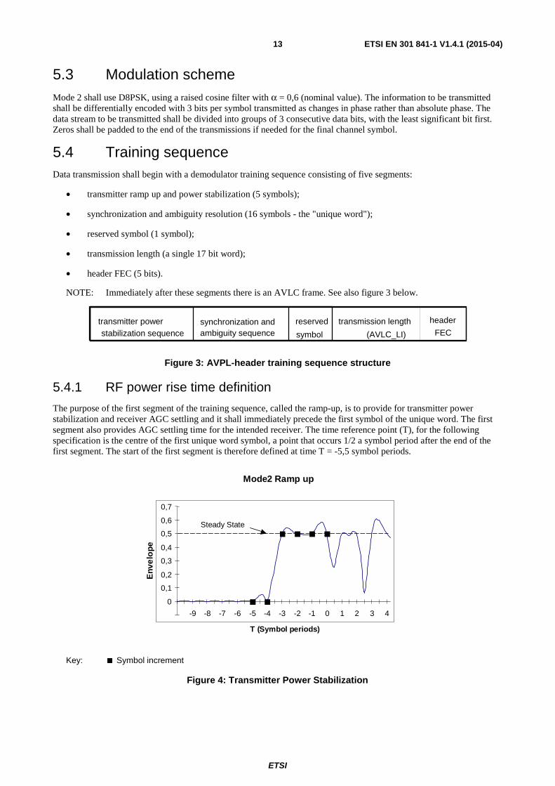
5.3 Modulation scheme Mode 2 shall use D8PSK, using a raised cosine filter with α = 0,6 (nominal value). The information to be transmitted shall be differentially encoded with 3 bits per symbol transmitted as changes in phase rather than absolute phase. The data stream to be transmitted shall be divided into groups of 3 consecutive data bits, with the least significant bit first. Zeros shall be padded to the end of the transmissions if needed for the final channel symbol.
5.4 Training sequence Data transmission shall begin with a demodulator training sequence consisting of five segments:
• transmitter ramp up and power stabilization (5 symbols);
• synchronization and ambiguity resolution (16 symbols - the "unique word");
• reserved symbol (1 symbol);
• transmission length (a single 17 bit word);
• header FEC (5 bits).
NOTE: Immediately after these segments there is an AVLC frame. See also figure 3 below.
transmitter power synchronization and reserved transmission length header stabilization sequence ambiguity sequence (AVLC_LI) symbol FEC
Figure 3: AVPL-header training sequence structure
5.4.1 RF power rise time definition
The purpose of the first segment of the training sequence, called the ramp-up, is to provide for transmitter power stabilization and receiver AGC settling and it shall immediately precede the first symbol of the unique word. The first segment also provides AGC settling time for the intended receiver. The time reference point (T), for the following specification is the centre of the first unique word symbol, a point that occurs 1/2 a symbol period after the end of the first segment. The start of the first segment is therefore defined at time T = -5,5 symbol periods.
Steady State
Mode2 Ramp up
0
0,1
0,2
0,3
0,4
0,5
0,6
0,7
-9 -8 -7 -6 -5 -4 -3 -2 -1 0 1 2 3 4
T (Symbol periods)
Env
elo
pe
Key: Symbol increment
Figure 4: Transmitter Power Stabilization

ETSI
ETSI EN 301 841-1 V1.4.1 (2015-04) 14
NOTE: There is a characteristic deep notch in the training sequence (see figure 4) which is located 2,5 symbol periods after the first synchronization symbol (T0). Therefore, the rf power level can be checked
5,5 symbol periods (524 µs) before this "marker" at T-3.
5.5 Physical layer Service Access Point The Physical Layer SAP protocol is based on the following primitives.
Primitive Parameters Value Comments AVPL_DATA.req AVLC_frame X From upper layers AVLC_LI Length of AVLC frame AVPL_DATA.ind AVLC_frame X To upper layers SQP 0 ÷ 15 AVPL_STATUS.ind CHANNEL STATUS BUSY/IDLE To upper layers
NOTE 1: Physical layer parameters (e.g.: maximum AVL length, operating frequency and test mode) are not handled by this SAP.
NOTE 2: Signal quality analysis is described in clause 6.4.3.3 Signal Quality Parameter.
5.6 Tuning range and channel increments The transceiver shall be capable of tuning to any of the 760 channels of 25 kHz width from 118,000 MHz to 136,975 MHz as defined in ICAO SARPS, Annex 10 Volume 1, part 1 [2].
6 VDL MODE 2 equipment requirements Unless otherwise stated all specifications shall be met under room conditions, at the nominal data rate, with the transceiver tuned to any 25 kHz channel within the range 118,000 MHz to 136,975 MHz.
6.1 Transmitter requirements Unless otherwise stated, these requirements are applicable to transmitters over the entire frequency range of 118,000 MHz to 136,975 MHz.
Unless otherwise stated, the reference bit sequence is specified as follows:
• The maximum "transmit" period is determined by the maximum "burst" length permitted for Mode 2 operation. The maximum burst length is 4,16 s at the nominal symbol rate of 10 500 symbols/s plus the synchronization sequence.
• The minimum "off" period is determined by the minimum transmitter "power down" time plus the minimum "channel idle" detection time plus the minimum value of the inter-access delay timer (TM1). According to ICAO SARPS, the minimum "off" period is 2 ms.
• The maximum duty cycle is therefore 4,16 s in "transmit" mode followed by 3,1 ms "off". The reference bit sequence shall not exceed 15 cycles.
6.1.1 Frequency Tolerance
The frequency of the rf carrier shall be within ±2 ppm of the selected frequency.
6.1.2 Manufacturer's declared output power
The carrier power is the mean rf power delivered to the coaxial matched impedance termination during transmission. The measured power shall be ±1 dB of the manufacturer's stated maximum output power.

ETSI
ETSI EN 301 841-1 V1.4.1 (2015-04) 15
6.1.3 Adjacent channel power
6.1.3.1 16 kHz channel bandwidth
The RF power measured over the 16 kHz channel bandwidth centred on the first adjacent channel shall not exceed -18 dBm.
6.1.3.2 25 kHz channel bandwidth
The RF power measured over the 25 kHz channel bandwidth centred on the first adjacent channel shall not exceed +2 dBm. The RF power measured over the 25 kHz channel bandwidth shall monotonically decrease at a minimum rate of 5 dB per octave beginning in the second adjacent channel from a maximum value of –28 dBm. Beginning in the fourth adjacent channel from a maximum value of –38 dBm the RF power measured over the 25 kHz channel bandwidth shall monotonically decrease at a minimum rate of 5 dB per octave down to a maximum value of -53 dBm. See also figure 5 below.
Figure 5: Maximum adjacent channel emissions
Maximum adjacent channel emissions
-60-55-50-45-40-35-30-25-20-15-10
-505
10
1 10 100Adjacent channel
dB
m

ETSI
ETSI EN 301 841-1 V1.4.1 (2015-04) 16
6.1.4 Conducted Spurious emissions
When the transmitter is "active" or "idle" (or the transceiver is in receive mode) and terminated in a matched impedance load, the power of any spurious emission at the output of the transmitter shall not exceed the values given in table 1.
Table 1
Environmental phenomena
Frequency range
Units Test limits, Tx Standby
Test limits Tx active mode
Reference bandwidth
Spurious conducted rf emissions
9 kHz to 150 kHz
dBm -57 (2 nW) -36 dBm B = 1 kHz
Spurious conducted rf emissions
> 150 kHz to 1 GHz
dBm -57 (2 nW) -36 dBm for harmonics, -46 dBm for non-harmonic
spurious
B = 10 kHz (see notes 1 and 2)
Spurious conducted rf emissions
> 1 GHz to 4 GHz
dBm -47 (20 nW) -30 dBm for harmonics -40 dBm for non-harmonic
spurious
B = 10 kHz
NOTE 1: For transmitters with an rf output above 50 W a limit of -80 dBc will be applied for harmonically related spurious. NOTE 2: An exclusion band of ±1 MHz about the carrier shall be used in active transmit mode.
6.1.5 Cabinet radiation
The transmitter shall meet the cabinet radiation requirements of ETSI EN 300 113-1 [3], clause 7.5.4, table 5.
6.1.6 Modulation rate
The Mode 2 symbol rate shall be 10 500 symbols/s ± 50 ppm, resulting in a nominal bit rate of 31 500 bits/s as defined in [1].
6.1.7 Intermodulation attenuation
The transmitter output intermodulation attenuation shall be at least 70,0 dB for any intermodulation component. In the case where the performance is achieved by additional internal or external isolating devices (such as circulators) these are expected to be available at the time the measurements are made and shall be used for the measurements [3].
For sites where no other transmitter is in service this value may be reduced by the licensing regulatory authority to a minimum of 40 dB.
6.1.8 RF power rise time
The transmitter output power shall achieve at least 90 % of the manufacturers' declared output power level in a time less than 190 µs (two symbols).
The transmitted output power shall be less than -40 dBc prior to the start of the first segment (T0 - 5,5 symbol periods).
The transmitter power stabilization segment shall consist of 5 symbols each representing 000 (2 symbols for the rf power rise time and 3 symbols for the receiver AGC stabilization).
NOTE: In order to minimize the transient effect of power rising on an adjacent channel, attention should be paid to the profile of the rf signal during the ramp-up period.
6.1.9 RF power release time
The transmitter output power shall decay at least 20 dB below the manufacturers' declared output power level (see clause 6.2.2) within 300 µs after transmitting the final information symbol.
NOTE: In order to minimize the transient effect of power decreasing on an adjacent channel, attention should be paid to the profile of the rf signal during the ramp-down period.

ETSI
ETSI EN 301 841-1 V1.4.1 (2015-04) 17
6.1.10 Transceiver timing requirements
6.1.10.1 Receiver to transmitter turn-around time
When the MAC persistence parameter is set to p=1, a ground station shall transmit the training sequence such that the center of the first symbol of the unique word will be transmitted no more than 2,75 ms after the received signal falls below -100 dBm.
6.1.10.2 Transmitter to receiver turn-around time
A ground base station shall be capable of receiving and demodulating an incoming signal within 1,5 ms after transmitting the final information symbol.
6.1.11 Symbol constellation error
The RMS Error Vector Magnitude (EVM), when measured over the first 30 symbols of the reference bit sequence, shall be less than 6 %.
6.1.12 Protection of the transmitter
The protection of the transmitter represents the ability of the transmitter to be protected against malfunction due to faults in the antenna system. Worst case mis-matches are represented by a short and open circuit test. The transmitter shall operate normally after the completion of the test.
6.1.13 Load VSWR capability
When a 2:1 mismatch is applied to the transmitter output terminals by a length of feeder, which is varied in electrical length by up to half a wavelength, the requirements of clause 6.1.3 shall be met. In addition, the power output shall not be less than -3 dB of the manufacturers' declared value (see clause 6.1.2).
6.2 Receiver requirements The uncorrected BER requirement shall be equal to, or better than 10-3.
The reference signal level applied at the receiver input for all receiver requirements, unless otherwise stated, is -87 dBm.
6.2.1 Sensitivity
A maximum signal level of -98 dBm from a modulated VDL Mode 2 signal source shall produce the uncorrected BER requirement specified in clause 6.2.
6.2.2 Co-channel interference
The uncorrected BER requirement (see clause 6.1) shall be achieved when a VDL Mode 2 interfering signal, -20 dB below the reference level, is applied in addition to the reference signal level.
6.2.3 First Adjacent Channel Rejection
The minimum adjacent channel rejection ratio (ACR) shall be determined in the presence of the reference signal level (see clause 6.2).
The ACR required to achieve the uncorrected BER (see clause 6.2) shall be equal to, or greater than, 44 dB. The test shall be performed on each side (±25 kHz) of the wanted signal.

ETSI
ETSI EN 301 841-1 V1.4.1 (2015-04) 18
6.2.4 Rejection of signals within the VHF Aeronautical band
The uncorrected BER requirement (see clause 6.2) shall be achieved when the wanted signal, set at the reference signal level (see clause 6.1), is combined with an unmodulated interfering signal in the following conditions:
a) Level of the interfering signal set at -33 dBm at frequencies corresponding to second and third adjacent channels centre.
b) Level of the interfering signal set at -27 dBm at frequencies corresponding to fourth adjacent channels centre.
c) Level of the interfering signal set at -27 dBm at a separation of ±1 MHz from the nominal receiver frequency.
6.2.5 Rejection of signals outside the VHF Aeronautical band
The uncorrected BER requirement (see clause 6.2) shall be achieved when one of the specified unwanted signals is applied and when the wanted signal is set at the reference signal level (see clause 6.2).
Unwanted signal A:
Level: -33 dBm.
Modulation: None.
Frequency range: 108,000 MHz to 156,000 MHz (excluding 117,950 MHz to 137,025 MHz).
Unwanted signal B:
Level: -7 dBm.
Modulation: None.
Frequency range: 50 kHz to 1 215,000 MHz (excluding the range 87,500 MHz to 156,000 MHz).
NOTE 1: A maximum interfering level of -33 dBm is permitted at the receiver IF frequencies.
Unwanted signal C:
Level: -5 dBm.
Modulation: None.
Frequency range: 87,500 MHz to 107,900 MHz.
NOTE 2: It is recommended that the frequency ranges are swept at a rate not exceeding 1,5 × 10⁻³ decades/s. Where the frequency range is swept incrementally, it is recommended that the step size does not exceed 1 % of the previous frequency.
6.2.6 In-band Intermodulation
The aim of the following requirement is to specify the receiver linearity in order to guarantee the third order interception point (IP3) is at least 0 dBm.
The uncorrected BER requirement (see clause 6.2) shall be achieved in the presence of two interfering signals, displaced in frequency, from the desired signal.
Desired signal:
Level: -75 dBm.
Modulation: VDL Mode 2.
Frequency: 118,000 MHz, 127,500 MHz, 136,975 MHz.
Unwanted signal A:
Level: -32 dBm.

ETSI
ETSI EN 301 841-1 V1.4.1 (2015-04) 19
Modulation: None.
Frequency: test frequency ± 1 MHz.
Unwanted signal B:
Level: -32 dBm.
Modulation: VDL Mode 2 (or simulated Mode 2).
Frequency: test frequency ± 2 MHz.
6.2.7 Desired signal dynamic range
The receiver shall continue to achieve the uncorrected BER requirement (see clause 6.2) when the desired signal level is increased from the reference signal level to a level of -7 dBm.
6.2.8 Conducted spurious emission
When the receiver input is terminated in a matched impedance, the level of any spurious emission appearing across the load shall not exceed -57 dBm over the frequency range of 9 kHz to 1 GHz and -47 dBm over the frequency range of 1 GHz to 4 GHz, with the exception of the range of 108,000 MHz to 137,000 MHz, where it shall not exceed -64 dBm.
6.2.9 Cabinet radiation
The receiver shall meet the cabinet radiation requirements of ETSI EN 300 113-1 [3], clause 8.10.4, table 14.
6.2.10 Symbol rate capture range
The uncorrected BER requirement (see clause 6.2) shall be achieved when the reference signal level is subject to a symbol rate offset of ±50 ppm.
6.2.11 Frequency capture range
The receiver shall be capable of acquiring and maintaining a lock to any selected channel with the maximum permitted signal frequency offset.
The uncorrected BER requirement (see clause 6.2) shall be achieved when the reference signal level is subject to a frequency offset of ±826 Hz. This value is composed of the maximum transmitter frequency error at 136,975 MHz (±685 Hz) and the maximum Doppler shift (±141 Hz).
6.3 Void
6.4 MAC sub-layer requirements
6.4.1 MAC services
6.4.1.1 Multiple Access
The MAC sublayer shall implement the non-adaptive p-persistent CSMA algorithm defined in section 3.2.1.1 of the Manual [4].
6.4.1.2 Channel Congestion
The MAC sub-layer shall notify the VME sub-layer whenever channel congestion is detected.
6.4.2 MAC System Parameters
6.4.2.1 Timer TM1 (inter-access delay timer)
The TM1 timer shall be set to the time that a MAC sub-layer will wait between consecutive access attempts

ETSI
ETSI EN 301 841-1 V1.4.1 (2015-04) 20
6.4.2.2 Timer TM2 (channel busy timer)
The VME shall be notified after the expiration of the Timer TM2 (channel busy timer).
6.4.2.3 Parameter p (persistence)
The MAC sub-layer shall implement a p-persistent CSMA algorithm.
6.4.2.4 Counter M1 (maximum access attempts)
The counter M1 shall be set to the maximum number of attempts (M1) that a MAC sub-layer will make for any transmission request.
6.4.3 Description of MAC Layer Procedures
6.4.3.1 Channel Sensing
The MAC sub-layer shall implement a channel sensing.
6.4.3.2 Access Attempt
An access attempt shall be made when the channel transitions from busy to idle.
6.4.3.3 Signal Quality Parameter
The SQP value shall be sent to the AVLC layer. Signal quality analysis shall be performed on the demodulator evaluation process and on the receive evaluation process; this analysis shall be normalized between a scale of 0 and 15, where 0 represents a received signal strength lower than -100 dBm and 15 for a signal strength higher than -72 dBm. SQP values between -100 dBm and -72 dBm are determined in table 2.
Table 2
SQP Value RSSI Power Range (dBm)
0 P < -100 1 -100 ≤ P < -98 2 -98 ≤ P < -96 3 -96 ≤ P < -94 4 -94 ≤ P < -92 5 -92 ≤ P < -90 6 -90 ≤ P < -88 7 -88 ≤ P < -86 8 -86 ≤ P < -84 9 -84 ≤ P < -82
10 -82 ≤ P < -80 11 -80 ≤ P < -78 12 -78 ≤ P < -76 13 -76 ≤ P < -74 14 -74 ≤ P < -72 15 -72 ≤ P
6.4.4 Services (Part of DLS)
6.4.4.1 Error Detection
The DLS sublayer shall detect and discard all frames corrupted during transmission.
6.4.4.2 Station Identification
The DLS sublayer shall accept (over a point-to-point connection) only frames that are addressed to it.
ETSI
ETSI EN 301 841-1 V1.4.1 (2015-04) 21
7 General requirements
7.1 General The equipment shall be able to operate on all channels in the list of assignable frequencies defined in Group A to E of appendix to chapter 4 of the ICAO, Annex 10 Volume V [2].
It shall not be possible to transmit while any frequency synthesizer used within the transmitter is out of lock.
It shall not be possible to transmit during channel switching operations.
7.2 Controls and indicators The equipment shall have the following controls and indicators as a minimum:
• a visual indication that the device is switched on;
• a visual indication that the carrier is being produced.
7.3 Class of emission and modulation characteristics The equipment shall use D8PSK modulation with the emission designator 14K0G1DE (see ITU Radio Regulations [i.7]). The equipment shall be designed to operate satisfactorily with a channel separation of 25 kHz.
7.4 Warm up After being switched on the equipment shall be operational within five seconds and shall be able to meet the performance requirements of the present document within one minute under normal conditions.
8 Test conditions, power sources and ambient temperatures
8.1 Test power source During testing, the equipment shall be supplied from a test power source capable of producing normal and extreme test voltages as specified in clauses 8.2.1.2, 8.2.2.3 and 8.2.2.4.
The internal impedance of the test power source shall be low enough for its effect on the test results to be negligible. For the purpose of testing the power source voltage shall be measured at the input terminals of the equipment.
During testing, the power source voltages shall be maintained within a tolerance of ±3 % relative to the voltage level at the beginning of each test.
8.2 Normal and extreme test conditions Measurements shall be made under normal test conditions and also, where stated, under extreme test conditions.
8.2.1 Normal test conditions
8.2.1.1 Normal temperature and humidity
The normal temperature and humidity conditions for tests shall be a combination of temperature and humidity within the following ranges:
• temperature: +15 °C to +35 °C;
• relative humidity: 20 % to 75 %.
ETSI
ETSI EN 301 841-1 V1.4.1 (2015-04) 22
When it is impracticable to carry out the tests under these conditions, a note to this effect, stating the ambient temperature and relative humidity during the tests, shall be added to the test report.
8.2.1.2 Normal power sources
8.2.1.2.1 Mains voltage and frequency
The normal test voltage for equipment to be connected to the mains shall be the nominal mains voltage.
For the purpose of the present document, the nominal voltage shall be the declared voltage or any of the declared voltages for which the equipment was designed.
The frequency of the test power source shall correspond to the appropriate AC mains.
8.2.1.2.2 Other power sources
For operation from other power sources, the normal test voltage shall be that declared by the equipment manufacturer.
8.2.2 Extreme test conditions
8.2.2.1 Extreme temperatures
For tests at extreme temperatures, measurements shall be made at a lower temperature of -10 °C and an upper temperature of +55 °C. This test shall be performed at the nominal supply voltage as defined in clause 8.2.1.2.1.
8.2.2.2 Procedure for tests at extreme temperatures
8.2.2.2.1 General
The equipment shall be switched off during the temperature stabilizing periods.
For tests at the upper temperature on equipment designed for continuous operation, the equipment shall be placed in the test chamber and left until thermal equilibrium is reached. The equipment shall then be switched on for 30 minutes before measurements are made. Transmitters shall be operated in the highest rated power transmit condition in that 30 minutes period before measurements are made.
For tests at the lower temperature, the equipment shall be left in the test chamber until thermal equilibrium is reached. The equipment shall then be switched on for 1 minute in the standby or receive condition before measurements are made.
8.2.2.2.2 High temperature
• Place the equipment in a chamber and heat to 55 ºC (±3 ºC) and allow to stabilize for 1 hour.
• Switch on the equipment (transmitters shall be keyed).
• After 30 minutes carry out a performance check as detailed in clause 8.4.2.
• Switch off the equipment and allow the chamber to cool to room temperature over a 1 hour period.
• Allow time for the equipment to stabilize to normal room temperature and humidity before carrying out the next test.
8.2.2.2.3 Low temperature
• Place the equipment in a chamber and cool to -10 ºC (±3 ºC) for 2 hours.
• Switch on the equipment and maintain the chamber operating temperature at -10 ºC (±3 ºC).
• After 1 minute carry out a performance check as detailed in clause 8.4.2.
• Switch off the equipment and allow the chamber to rise to room temperature over a 1 hour period.
• Allow time for the equipment to stabilize to normal room temperature and for moisture to disperse before carrying out the next test.

ETSI
ETSI EN 301 841-1 V1.4.1 (2015-04) 23
8.2.2.3 Extreme values of test power sources
Mains voltage
• The extreme test voltages shall be ±10 % of the value declared in clause 8.2.1.2.1.
• The frequency of the test voltage shall be the nominal frequency of the supply as declared in clause 8.2.1.2.1.
• This test shall be performed at the normal temperature and humidity as defined in clause 8.2.1.1.
8.2.2.4 Other power sources
For equipment using other power sources, or capable of being operated from a variety of power sources, the extreme test voltages shall be those agreed between the equipment manufacturer and the testing laboratory and shall be recorded in the test report.
8.3 Test channels Tests shall be carried out on at least three channels:
• 118,000 MHz.
• 127,500 MHz.
• 136,975 MHz.
8.4 General conditions of measurement
8.4.1 Receiver test signal arrangement
Test signal sources shall be connected to the receiver input in such a way that the impedance presented to the receiver input is 50 Ω ± 2 Ω, irrespective of whether one or more test signals are applied to the receiver simultaneously.
8.4.2 Receiver BER test
A BER test shall use a VHF signal generator representing the desired source signal and external BER test equipment (e.g. a computer and test software or Arbitrary Waveform Generator (AWG) interfaced to the VHF signal generator in vector modulation mode) which receives each burst payload from the receiver.
Uncorrected BER mode
A method for placing the receiver into the uncorrected BER mode shall be provided by manufacturers. The uncorrected BER mode is distinct from the operational mode.
The uncorrected BER mode is used to measure the uncorrected BER requirement.
1) The receiver shall forward each burst payload to the external BER test equipment without error detection or correction procedures.
2) The test payload shall be forwarded to the external BER test equipment only if the burst was successfully detected via the standard 16 symbols synchronization sequence.
VHF signal generators
Receiver test procedures require the use of a high performance VHF signal generator in order to permit high precision measurement. This VHF signal generator shall be capable of the specified modulation format and transmission waveform.
1) The VHF signal generator shall support transmission of VDL test bursts consisting of the ramp up period plus the standard 16 symbols synchronization sequence followed by a variable length test message, up to the maximum length of 43 771 symbols.
2) An external interface to the VHF signal generator shall be provided in order that the test payload can be provided via the external BER test equipment.

ETSI
ETSI EN 301 841-1 V1.4.1 (2015-04) 24
External BER test equipment
1) The test payload provided by the external BER test equipment shall be mapped directly into the burst payload in Mode-2 format. The formatting shall include Cyclic Redundancy Check (CRC), interleaving, scrambling and header.
NOTE: Forward Error Correction (FEC) may be encoded or left null, as this information will not be used when the receiver is configured to output "uncorrected" BER messages.
2) Unless otherwise stated, tests shall be conducted with maximum length Mode-2 messages.
3) The external BER test equipment generating the test payload for transmission by the VHF signal generator, and receiving/processing the received test payload shall be synchronized either explicitly (via a direct connection) or implicitly (by knowledge of the test payload).
4) Calculation of cumulative BER statistics shall begin once synchronization of the external BER test equipment between the transmitting and receiving burst payload has been accomplished. The receiving external BER test equipment shall detect the loss of an entire burst implicitly by lack of a burst payload message in the given burst period. Each test should include a running count of synchronization failures in addition to the cumulative BER.
Interfering (or undesired) source
Tests for CCI and ACR with the VDL waveform as the interfering signal shall be performed with the interfering signal applied in a continuous (non-pulsed) manner. The waveform shall simulate a VDL Mode-2 signal. Tests have shown that a suitable interfering source is a VHF signal generator configured to produce a narrow-band FM signal modulated with a 400 Hz tone at a peak frequency deviation of 5,25 kHz.
Figure 6 shows the basic test setup for receiver BER tests.
VDL ReceiverUnder Test
(in BER test mode)
UndesiredVDL Source
(if applicable for test)
DesiredVDL
Source
RFCombiner
BER TestEquipment
Test payloadcomprising N bits
N bits from test payloadsuccessfully detected byreceiver
Continous,simulatedD8PSK signal
RF test bursts
Figure 6: Receiver BER measurement
8.4.3 Performance check
Whilst the equipment is being subjected to the normal or extreme test conditions, establish compliance with the requirements of clauses 6.2.1 Sensitivity (Rx); 6.1.2 Manufacturer's declared output power (Tx) and 6.1.1 Frequency Tolerance (Tx).

ETSI
ETSI EN 301 841-1 V1.4.1 (2015-04) 25
9 Detailed Test Procedures for the physical layer The following test procedures provide a satisfactory means of establishing compliance with the requirements of clause 6. However, alternative test procedures, which provide equivalent information, may be used.
9.1 Transmitter
9.1.1 Frequency Error
The equipment requirements are specified in clause 6.1.1.
9.1.1.1 Definition
The frequency error is the difference between the measured carrier frequency and its nominal value.
9.1.1.2 Method of measurement
The carrier frequency shall be measured in the absence of modulation, with the transmitter connected to a coaxial termination. Measurements shall be made under extreme test conditions.
9.1.1.3 Limits
The frequency error shall be within the limits defined by clause 6.1.1.
9.1.2 Manufacturer's declared output power
The equipment requirements are specified in clause 6.1.2.
The following equipment is required:
• Transmission generator, PC with suitable software.
• Attenuator 30 dB.
• Power meter, with pulse power measurement facility or vector signal analyser.
The measurement procedure consists of the following steps:
Step 1: Connect the equipment as shown in figure 7.
Step 2: Tune the transmitter to one of the test frequencies (see clause 8.3).
Step 3: Key the transmitter under test "on" and modulate the carrier with continuous maximum length Mode 2 messages from the transmission generator.
Step 4: Set the power meter (or VSA) to capture the Mode 2 transmitted signal and determine the average transmitter output power during the message period.
Step 5: Repeat steps 2 to 4 at the two remaining test channels.
Step 6: Check that the measured output power is consistent with the manufacturer's declared output power according to clause 6.1.2, and remains so at all three test channels.
NOTE: It is recommended that the output power delivered into a 50 Ω load is measured during signal transmission and is not averaged over the time intervals between signal transmissions.

ETSI
ETSI EN 301 841-1 V1.4.1 (2015-04) 26
UnitUnder Test
TransmissionGenerator
PC + Software
Attenuator30 dB ProbeInput
Power Meter
Figure 7: Output power measurement
9.1.3 Adjacent channel power
The equipment requirements are specified in clause 6.1.3.
9.1.3.1 Method of measurement for the first adjacent channel
The following equipment is required:
• Transmission Generator, PC with suitable software.
• Attenuator 30 dB.
• Spectrum analyser with power band marker function.
The measurement procedure consists of the following steps:
Step 1: Connect the equipment as shown in figure 8.
Step 2: Tune the transmitter to one of the test frequencies.
Step 3: Key the transmitter under test "on" and modulate it with the transmission generator to produce continuous maximum length Mode 2 messages.
Step 4: Adjust the attenuator in the analyser to the minimum value which does not overload the input stage of the unit.
Step 5: Using 100 kHz span display the Mode 2 signal envelope. Use the analyser IF signal power as the trigger source for the display and set averaging to 10.
Step 6: Using the power band marker function of the analyser measure the power in a 16 kHz bandwidth, of the first upper adjacent channel.
Step 7: Repeat steps 3 to 6 for the first lower adjacent channel.
Step 8: Record the highest of the two measured values. Check that the first adjacent channel power is lower than the first adjacent channel power requirement (defined in clause 6.1.3).
Step 9: Repeat steps 2 to 8 at the two remaining test frequencies.
UnitUnder Test
TransmissionGenerator
PC + Software
Attenuator30 dB
Input Spectrum Analyser
Figure 8: First adjacent channel power measurement
ETSI
ETSI EN 301 841-1 V1.4.1 (2015-04) 27
9.1.3.2 Method of measurement for the second adjacent channel
The following equipment is required:
• Transmission Generator, PC with suitable software.
• Attenuator 30 dB.
• VHF crystal filter with a 3 dB bandwidth of 25 kHz and, with attenuation in excess of 50 dB at ±50 kHz.
• Spectrum analyser with power band marker function.
The measurement procedure consists of the following steps:
Step 1: Connect the equipment as shown in figure 9.
Step 2: Tune the transmitter to one of the test frequencies.
Step 3: Offset the tuned frequency of the transmitter under test to 50 kHz above the VHF crystal filter centre frequency. Key the transmitter under test "on". Use the transmission generator to produce continuous maximum length Mode 2 messages.
Step 4: Set the analyser span to 50 kHz and centre frequency to the centre frequency of the VHF crystal filter. Decrease the analyser input attenuator to the minimum level at which the attenuated rf signal from the transmitter under test does not overload the analyser. Use the analyser IF signal power as the trigger source for the display and set averaging to 10.
Step 5: Set analyser's power band marker function to 40 kHz. Notice that the measurement bandwidth is defined by the VHF crystal filter and setting the power band marker to the same bandwidth will give an erroneous result.
Step 6: Determine the second lower adjacent channel power.
Step 7: Repeat steps 3 to 6 with the transmitter under test tuned to 50 kHz below the crystal filter. Determine the second upper adjacent channel power.
Step 8: Record the second adjacent channel power as the highest of the two measured values.
Step 9: Check that the second adjacent channel power is less than the second adjacent channel power requirement (defined in clause 6.1.3).
Step 10: Repeat steps 2 to 9 at the two remaining test frequencies.
NOTE: To protect the analyser, ensure that the transmitter cannot be keyed "on", at the frequency of the crystal filter used for this test.
Transmission Generator PC
& Software
Unit under Test
VSA 10 dB 30 dB 30W
VHF Crystal
Filter
Figure 9: Second and fourth adjacent channel power measurement
9.1.3.3 Method of measurement for the fourth adjacent channel
The following equipment is required:
• Transmission Generator, PC with suitable software.
• Attenuator 30 dB.
• VHF crystal filter with a 3 dB bandwidth of 25 kHz and, with attenuation in excess of 50 dB at ±50 kHz.
• Spectrum analyser with power band marker function.

ETSI
ETSI EN 301 841-1 V1.4.1 (2015-04) 28
The measurement procedure consists of the following steps:
Step 1: Connect the equipment as shown in figure 9.
Step 2: Tune the transmitter to one of the test frequencies.
Step 3: Offset the tuned frequency of the transmitter under test to 100 kHz above the VHF crystal filter centre frequency. Key the transmitter under test "on". Use the transmission generator to produce continuous maximum length Mode 2 messages.
Step 4: Set the analyser span to 50 kHz and centre frequency to the centre frequency of the VHF crystal filter. Decrease the analyser input attenuator to the minimum level at which the attenuated rf signal from the transmitter under test does not overload the analyser. Use the analyser IF signal power as the trigger source for the display and set averaging to 10.
Step 5: Set analyser's power band marker function set to 40 kHz. Notice that the measurement bandwidth is defined by the VHF crystal filter and setting the power band marker to the same bandwidth will give an erroneous result.
Step 6: Determine the fourth lower adjacent channel power.
Step 7: Repeat steps 3 to 6 with the transmitter under test tuned to 100 kHz below the crystal filter. Determine the fourth upper adjacent channel power.
Step 8: Record the fourth adjacent channel power as the highest of the two measured values.
Step 9: Check that the fourth adjacent channel power is less than the fourth adjacent channel power requirement (defined in clause 6.1.3).
Step 10: Repeat steps 2 to 9 at the two remaining test frequencies.
An alternative Measurement Procedure for Adjacent Channel Power (ACP) consists of the following steps:
Step 1: Connect the equipment as shown in figure 12.
Step 2: Tune the transmitter to one of the test frequencies.
Step 3: Start the transmission generator that produces transmit blocks and simulates the transmit/receive duty cycle.
Step 4: Use an attenuator to protect the measurement equipment and a notch filter centred on the carrier frequency, if the dynamic range of the spectrum analyser is not sufficient. Set the spectrum analyser resolution bandwidth (Br) much narrower than the channel bandwidth and the video bandwidth (Bv) equal to ten times Br in order to avoid errors due to video averaging of noise.
Step 5: Measure and store the rf signal spectrum centred on the carrier frequency with a frequency span wide enough to display all the modulation spectrum between the -80 dB points, referred to the peak value.
Step 6: Convert the logarithmic trace values from the spectrum analyser to linear spectral power densities by the relation:
PBi
PidBm
n
= 10 10
where: PidBm = trace values (dBm).
Bn = effective noise bandwidth of the spectrum analyser (Hz).
Pi = spectral power densities (mW/Hz).
NOTE: Bn = k × Br, where k is a constant specified for each spectrum analyser.
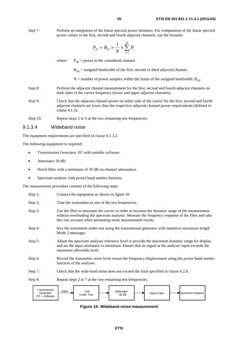
ETSI
ETSI EN 301 841-1 V1.4.1 (2015-04) 29
Step 7: Perform an integration of the linear spectral power densities. For computation of the linear spectral power values in the first, second and fourth adjacent channels, use the formula:
P B
NPch ch i
i
N
= × ×=∑
1
1
where: Pch = power in the considered channel.
Bch = assigned bandwidth of the first, second or third adjacent channel.
N = number of power samples within the limits of the assigned bandwidth, Bch.
Step 8: Perform the adjacent channel measurement for the first, second and fourth adjacent channels on both sides of the carrier frequency (lower and upper adjacent channels).
Step 9: Check that the adjacent channel power on either side of the carrier for the first, second and fourth adjacent channels are lower than the respective adjacent channel power requirements (defined in clause 6.1.3).
Step 10: Repeat steps 2 to 9 at the two remaining test frequencies.
9.1.3.4 Wideband noise
The equipment requirements are specified in clause 6.1.3.2.
The following equipment is required:
• Transmission Generator, PC with suitable software.
• Attenuator 30 dB.
• Notch filter with a minimum of 30 dB on-channel attenuation.
• Spectrum analyser with power band marker function.
The measurement procedure consists of the following steps:
Step 1: Connect the equipment as shown in figure 10.
Step 2: Tune the transmitter to one of the test frequencies.
Step 3: Use the filter to attenuate the carrier in order to increase the dynamic range of the measurement without overloading the spectrum analyser. Measure the frequency response of the filter and take this into account when presenting noise measurement results.
Step 4: Key the transmitter under test using the transmission generator with repetitive maximum length Mode 2 messages.
Step 5: Adjust the spectrum analyser reference level to provide the maximum dynamic range for display and set the input attenuator to minimum. Ensure that no signal at the analyser input exceeds the maximum allowable level.
Step 6: Record the transmitter noise level versus the frequency displacement using the power band marker function of the analyser.
Step 7: Check that the wide-band noise does not exceed the limit specified in clause 6.2.9.
Step 8: Repeat steps 2 to 7 at the two remaining test frequencies.
UnitUnder Test
TransmissionGenerator
PC + Software
Attenuator30 dB Notch Filter
InputSpectrum Analyser
Figure 10: Wideband noise measurement

ETSI
ETSI EN 301 841-1 V1.4.1 (2015-04) 30
9.1.4 Spurious emissions
The equipment requirements are specified in clause 6.1.4.
The following equipment is required:
• Transmission Generator, PC with suitable software.
• Attenuator 30 dB.
• Notch filters or bandpass filters, to suppress the on-channel signal by at least 60 dB.
• Spectrum analyser with power band marker function.
The measurement procedure consists of the following steps:
Step 1: Connect the equipment as shown in figure 11.
Step 2: Tune the transmitter to one of the test frequencies.
Step 3: Use the filters to reject the on-channel signal in order to increase the dynamic range of the measurement without overloading the spectrum analyser.
Step 4: Set the transmission generator to produce continuous maximum length Mode 2 messages and key the transmitter under test "on".
Step 5: Adjust the spectrum analyser reference level to provide the maximum dynamic range for display and set the input attenuator to minimum required to ensure that no signal at the analyser input exceeds the maximum allowable level.
Step 6: Measure the power level at each visible spurious signal using power band markers appropriate to the bandwidths specified in clause 6.1.4.
Step 7: Measure the frequency response of the filter and take this into account when presenting spurious measurement results. If a bandpass filter is used, it will need to be tuned to several measurement frequencies, covering the overall measured frequency range.
Step 8: Check that the results do not exceed the limits specified in clause 6.1.4.
Unit
Under Test
Transmission Generator
PC + Software
Attenuator 30 dB / 30 W Notch Filter
Input Spectrum Analyser
Figure 11: Spurious emissions measurement
9.1.5 Cabinet Radiation
The equipment requirements are specified in clause 6.1.5.
The required equipment is as described in ETSI EN 300 113-1 [3], clause 7.5.3.
9.1.6 Void
9.1.7 Inter-modulation attenuation
The equipment requirements are specified in clause 6.1.7.
The required equipment is as described in ETSI EN 300 113-1 [3], clause 7.6.2.

ETSI
ETSI EN 301 841-1 V1.4.1 (2015-04) 31
9.1.8 RF power rise time
The equipment requirements are specified in clause 6.1.8.
The following equipment is required:
• Transmission Generator, PC with suitable software.
• Attenuator 30 dB.
• VSA.
The measurement procedure shall be carried out at 127,500 MHz and consists of the following steps:
Step 1: Connect the equipment as shown in figure 12.
Step 2: Configure the vector analyser to display both constellation diagram and power versus time charts shown in figure 13.
Step 3: Use the transmission generator to produce a Mode 2 message and capture the start of this message.
Step 4: Using both constellation and power versus time display identify the first symbol of the synchronization sequence.
Step 5: At a time 3 symbol periods before the first synchronization symbol (defined in clause 5.4.1) record the rf power level.
Step 6: Check that the rf power rise time (defined in clause 6.1.8) is achieved.
Unit
Under Test Transmission
Generator PC + Software
Attenuator 30 dB / 30 W
Vector Signal Analyser
Input
Synchronisation
Figure 12: RF power rise and release time measurement also suitable for symbol constellation error

ETSI
ETSI EN 301 841-1 V1.4.1 (2015-04) 32
Figure 13: VSA displays constellation diagram illustrating rf rise-time
NOTE: There is a characteristic notch in the synchronization sequence which is located 2,5 symbol periods after the first synchronization symbol. Therefore, it is easy to check the rf power level 5,5 symbol periods (524 µs) before this "marker". This could constitute an alternative method using a standard spectrum analyser or fast storage oscilloscope (see figure 13a).

ETSI
ETSI EN 301 841-1 V1.4.1 (2015-04) 33
Figure 13a: Oscilloscope displays illustrating rf rise-time
9.1.9 RF power release time
The equipment requirements are specified in clause 6.1.9.
The following equipment is required:
• Transmission Generator, PC with suitable software.
• Attenuator 30 dB.
• VSA.
The measurement procedure shall be carried out at 127,500 MHz and consists of the following steps:
Step 1: Connect the equipment as shown in figure 12.
Step 2: Configure the vector signal analyser in digital demodulation mode, to display log magnitude of I and Q vectors, with normalization disabled. Set the Y axis to read "dBm". The symbol times are displayed on the resultant profile of power versus time. Use of the trigger hold off function will aid signal acquisition.
Step 3: Using the transmission generator to produce a Mode 2 message. Capture the end of this message on the vector signal analyser.
Step 4: Use the power versus time display to determine the corresponding profile for each symbol of the "power down" ramp.
Step 5: Check that the rf power release time (defined in clause 6.1.9) is achieved.

ETSI
ETSI EN 301 841-1 V1.4.1 (2015-04) 34
9.1.10 Physical layer, system parameters
9.1.10.1 Receiver to Transmitter turn-around time
The equipment requirements are specified in clause 6.1.10.1.
The following equipment is required:
• Transmission Generator or PC with suitable software.
• 20 dB directional couplers.
• 30 dB attenuators.
• Pin diode attenuator.
• VHF signal generator.
• RF combiner.
• Vector signal analyser with power band marker function.
The measurement procedure consists of the following steps:
Step 1: Connect the equipment as shown in figure 14.
Step 2: Tune the transmitter to one of the test frequencies.
Step 3: Configure the VSA to display Power versus Time, external trigger enabled.
Step 4: Set the VHF signal generator to produce an on-channel CW signal of -80 dBm at the input to the equipment under test. Set the PIN diode attenuator to 0 dB.
Step 5: Use the transmission generator to set the MAC parameters for the equipment under test:
TM1 (Inter-access delay) = 0,5 ms.
TM2 (Channel busy) = 120 s.
P (Persistence) = 1.
M1 (Maximum number of attempts) = 65 535.
Step 6: Use the transmission generator to load the equipment under test with a Mode-2 message and request transmission of the message by the equipment under test.
Step 7: Use the computer control to set the pin diode attenuator to 20 dB and trigger the VSA.
Step 8: Use the VSA to confirm the -20 dB signal attenuation "step" occurred in an insignificant time. Measure the time interval until between the step and commencement of transmission, determined by the transmitter output achieving 90 % of manufacturers declared output power (see clause 6.1.2).
Step 9: After accounting for the minimum Inter-access time (TM1) calculate the "turn-around" time. Check that the maximum receive to transmit turn-around time (see clause 6.1.10.1) has not been exceeded.
ETSI
ETSI EN 301 841-1 V1.4.1 (2015-04) 35
Signal Generator
Pin Attenuator
30 dB Attenuator
50 dB Attenuator
Unit under Test
Vector Signal
Analyser
Transmission Generator /
Control Computer
RF Combiner Hybrid
20 dB Coupler 20 dB Coupler
Figure 14: Receiver to transmitter turn-around measurement
9.1.10.2 Transmitter to Receiver turn-around time
The equipment requirements are specified in clause 6.1.10.2.
Equipment Required:
• Transmission Generator or PC with suitable software.
• Arbitrary Waveform Generator (AWG).
• 20 dB directional couplers.
• 30 dB attenuators.
• VHF signal generator suitable for digital modulation.
• RF combiner.
• Vector signal analyser with power band marker function.
The measurement procedure consists of the following steps:
Step 1: Connect the equipment as shown in figure 15.
Step 2: Tune the transceiver to one of the test frequencies.
Step 3: Configure the VSA to display Power versus Time, external trigger enabled.
Step 4: Set the signal generator to provide a signal of -60 dBm at the input of the equipment under test.
Step 5: Load the AWG with a valid Mode 2 message.
Step 6: Use the transmission generator to set the MAC parameters for the equipment under test:
TM1 (Inter-access delay) = 0,5 ms.
TM2 (Channel busy) = 120 s.
P (Persistence) = 1.
M1 (Maximum number of attempts) = 65 535.
Step 7: Load a Mode 2 message into the equipment under test. Request transmission of this message and trigger the VSA.
ETSI
ETSI EN 301 841-1 V1.4.1 (2015-04) 36
Step 8: Record the time interval between the trigger event and the end of transmission from the equipment under test. Use the result to calculate the minimum time between the transmit request and the trigger event for the AWG.
Step 9: Load the equipment under test with a Mode 2 message, request transmission and, after the delay calculated in step 8, trigger the AWG to send its Mode 2 message.
Step 10: Check whether the equipment under test had successfully received the transmission from the AWG.
Step 11: If the AWG transmission was not correctly received, increase the AWG time delay and repeat steps 9 to 10 until the equipment under test has successfully received the messages from the AWG.
Step 12: Repeat steps 3 to 11 at the two remaining test frequencies.
Step 13: Check that the maximum transmit to receive turn-around time (see clause 6.1.10.2) has not been exceeded.
Arbitrary
Waveform Generator
Vector Signal
Generator
30 dB Attenuator
30 dB Attenuator
Unit under Test
Vector Signal
Analyser
Transmission Generator /
Control Computer
RF Combiner Hybrid
20 dB Coupler 20 dB Coupler
Figure 15: Transmitter to receiver turn-around time measurement
9.1.11 Symbol Constellation Error
The equipment requirements are specified in clause 6.1.11.
The following equipment is required:
• Transmission generator, PC with suitable software.
• Attenuator 30 dB.
• Vector Signal analyser.
The measurement procedure consists of the following steps:
Step 1: Connect the equipment as shown in figure 12.
Step 2: Tune the transmitter to one of the test frequencies.
Step 3: Tune the vector signal analyser to the correct channel frequency and modulation scheme, select a suitable level range.
Step 4: Key the transmitter under test "on" and modulate it with continuous maximum length Mode 2 messages produced by the transmission generator.
Step 5: Record the RMS EVM error at symbol centres.

ETSI
ETSI EN 301 841-1 V1.4.1 (2015-04) 37
Step 6: Check that the results are within the limits specified in clause 6.1.11.
Step 7: Repeat steps 2 to 6 at the two remaining test frequencies.
9.1.12 Protection of the transmitter
The equipment requirements are specified in clause 6.1.12.
9.1.12.1 Method of measurement
While the transmitter is transmitting at the rated output power, the antenna port shall first be short-circuited and then open-circuited, in each case for a period of 1 minute. This test shall be performed on the centre test frequency only.
9.1.12.2 Requirement
This test shall not result in any damage to the transmitter. After removal of the short-circuit and open-circuit conditions, the transmitter shall meet the requirements of the Performance check (see clause 8.4.3).
9.1.13 Load VSWR capability
The equipment requirements are specified in clause 6.1.13.
The following equipment is required:
• Transmission Generator, PC with suitable software.
• 30 dB directional coupler.
• Adjustable delay line.
• 2:1 VSWR Resistive load.
• Vector signal analyser with power band marker function.
The measurement procedure consists of the following steps:
Step 1: Connect the equipment as shown in figure 16.
Step 2: Tune the transmitter to one of the test frequencies.
Step 3: Key the transmitter under test with the transmission generator with repetitive maximum length Mode 2 messages.
Step 4: Vary the VSWR phase angle of the load with the delay line and measure the minimum average forward rf output power from the Transmitter using the vector signal analyser power band marker function.
Step 5: Check that the minimum average forward rf output power is greater than the limit defined in clause 6.1.13.
Step 6: Repeat steps 2 to 5 at the two remaining test frequencies.
ETSI
ETSI EN 301 841-1 V1.4.1 (2015-04) 38
Transmission Generator PC &
SoftwareUnit under Test
2:1 VSWR Resistive Load
Delay Line
Vector Signal Analyser
30 dB Directional Coupler
Figure 16: LOAD VSWR CAPABILITY
9.2 Receiver
9.2.1 Sensitivity
The equipment requirements are specified in clause 6.2.1.
The following equipment is required:
• VHF Signal Generator.
• External BER test equipment.
The measurement procedure consists of the following steps:
Step 1: Connect the equipment as shown in figure 6 but notice that the rf combiner is not required for this test. Set the receiver under test into the uncorrected BER mode.
Step 2: Set the desired VDL source, (a VHF signal generator) to generate an input signal to the receiver at one of the test frequencies (see clause 8.3).
Step 3: Modulate the desired signal with the test payload (maximum burst length of symbols) provided by the external BER test equipment. Adjust the level of the signal generator to the maximum signal level (see clause 6.2.1) at the receiver input terminals.
Step 4: Repeat steps 2 and 3 at the two remaining test frequencies (see clause 8.3).
Step 5: Using the external BER test equipment, determine the uncorrected BER of the demodulated data at the receiver output. Check the sensitivity requirement (see clause 6.2.1) is achieved at all three test frequencies.
9.2.2 Co-channel interference
The equipment requirements are specified in clause 6.2.2.
The following equipment is required:
• 2 VHF Signal Generators.
• External BER test equipment.
• RF combiner.

ETSI
ETSI EN 301 841-1 V1.4.1 (2015-04) 39
The measurement procedure consists of the following steps:
Step 1: Connect the equipment as shown in figure 6, and set the receiver to the uncorrected BER mode.
Step 2: Use the Desired VDL Source (named A), to generate a desired input signal to the receiver.
Step 3: Tune the generator A to one of the test frequencies (see clause 8.3) and modulate the carrier with the test payload (maximum burst length of symbols) provided by the external BER test equipment. Adjust generator A to provide the reference signal level (see clause 6.2) at the receiver input terminals.
Step 4: Use the second signal generator (named B), to generate a co-channel interfering input signal to the receiver.
Step 5: Tune the signal generator B to the receiver channel frequency and configure it to produce a narrow band FM signal with a maximum peak deviation of ±5,25 kHz. Modulate generator B with a 400 Hz sine wave. Adjust generator B to produce an interfering signal level 20 dB below the reference signal level (see clause 6.2) at the receiver input terminals.
Step 6: Apply the desired signal and the co-channel interfering FM modulated signal to the receiver input via the rf combiner and measure the uncorrected BER of the demodulated data at the receiver output with the external BER test equipment.
Step 7: Repeat steps 2 to 6 at the two remaining test frequencies (see clause 8.3).
Step 8: Check that the uncorrected BER requirement (see clause 6.2) is achieved in all cases.
9.2.3 First Adjacent Channel Rejection
The equipment requirements are specified in clause 6.2.3.
The following equipment is required:
• 2 VHF Signal Generators.
• External BER test equipment.
• RF combiner.
The measurement procedure consists of the following steps:
Step 1: Connect the equipment as shown in figure 6 and set the receiver to the uncorrected BER mode.
Step 2: Adjust the Desired VDL Source (generator A), to produce an input signal to the receiver at one of the test frequencies (see clause 8.3).
Step 3: Modulate generator A with the test payload (maximum burst length of symbols) provided by the external BER test equipment. Adjust signal generator A to produce the reference signal level (see clause 6.2) at the receiver input terminals.
Step 4: Use the second VHF signal generator (named B), to generate an adjacent channel interfering input signal to the receiver.
Step 5: Tune generator B to the first upper adjacent channel frequency. Set generator B to produce a narrow-band FM signal (to simulate a second VDL Mode-2 source). Apply the desired input signal and the adjacent interfering signal to the receiver input via the rf combiner.
Step 6: Adjust the level of signal generator B until the uncorrected BER is reduced to the minimum requirement (see clause 6.2). Record the interfering signal level at the receiver input terminals.
Step 7: Repeat steps 5 and 6 for the lower adjacent channel.
Step 8: Determine the ratio between the interfering and desired signal levels for both upper and lower adjacent channels. Record these two ratios.
Step 9: Repeat steps 4 to 8 at the two remaining test frequencies (see clause 8.3).
ETSI
ETSI EN 301 841-1 V1.4.1 (2015-04) 40
Step 10: Check that the ACR requirement (defined in clause 6.2.3) is achieved in all cases.
NOTE: It is recommended that the noise sidebands of the interfering signal do not interfere with the desired signal in the receiver passband. The isolation offered by the rf combiner should be sufficient to prevent intermodulation between the VHF generators.
9.2.4 Rejection of signals within the VHF Aeronautical band
The equipment requirements are specified in clause 6.2.4.
The following equipment is required:
• 2 VHF Signal Generators.
• External BER test equipment.
• RF combiner.
NOTE: It is recommended that the noise sidebands of the interfering signal do not interfere with the desired signal in the receiver passband. The isolation offered by the rf combiner should be sufficient to prevent intermodulation between the VHF generators.
The measurement procedure consists of the following steps:
Step 1: Connect the equipment as shown in figure 6 - and set the receiver to the uncorrected BER mode.
Step 2: Adjust the Desired VDL Source, generator A, to produce an input signal to the receiver at one of the test frequencies (see clause 8.3).
Step 3: Modulate generator A with the test payload (maximum burst length of symbols) using the external BER test equipment. Adjust signal generator A to provide the reference signal level (see clause 6.1) at the receiver input terminals.
Step 4: Set the second signal generator (named B), to produce an unmodulated (cw) interfering signal to the receiver input.
Step 5: Tune generator B to the upper second adjacent channel and adjust the signal generator to the level defined in clause 6.2.4 a).
Step 6: Apply the wanted input signal and the unmodulated interfering signal to the receiver input via the rf combiner and determine the uncorrected BER of the demodulated data with the external BER test equipment.
Step 7: Repeat steps 5 and 6 for the lower second adjacent channel and the upper and lower third adjacent channels.
Step 8: Tune generator B to the upper fourth adjacent channel and adjust the signal generator to the level stated in clause 6.2.4 b).
Step 9: Apply the wanted input signal and the unmodulated interfering signal to the receiver input via the rf combiner and determine the uncorrected BER of the demodulated data with the external BER test equipment.
Step 10: Repeat steps 8 and 9 for the lower fourth adjacent channel.
Step 11: Tune generator B to +1 MHz from the nominal receiver frequency and adjust the signal generator to the level stated in clause 6.2.4 c).
Step 12: Apply the wanted input signal and the unmodulated interfering signal to the receiver input via the rf combiner and determine the uncorrected BER of the demodulated data with the external BER test equipment.
Step 13: Repeat steps 11 and 12 for -1 MHz from the nominal receiver frequency.
Step 14: Set the second signal generator (named B), to produce an unmodulated (cw) interfering signal to the receiver input.

ETSI
ETSI EN 301 841-1 V1.4.1 (2015-04) 41
Step 15: Repeat steps 5 to 14 at the other test frequencies (see clause 8.3).
9.2.5 Rejection of signals outside the VHF Aeronautical band
The equipment requirements are specified in clause 6.2.5.
The following equipment is required:
• 2 VHF Signal Generators.
• External BER test equipment.
• RF combiner.
The measurement procedure consists of the following steps:
Step 1: Connect the equipment as shown in figure 6 - and set the receiver to the uncorrected BER mode.
Step 2: Use the Desired VDL Source (generator A), to produce an input signal to the receiver at one of the test frequencies (see clause 8.3).
Step 3: Modulate generator A with the test payload (maximum burst length of symbols) using the external BER test equipment. Adjust signal generator A to provide the reference signal level (see clause 6.2) at the receiver input terminals.
Step 4: Use the second signal generator (named B), to generate one of the specified interfering signals at the receiver input.
Step 5: Tune generator B to any frequency defined in clause 6.2.5. Adjust the level of generator B to provide the interfering signal level also defined in clause 6.2.5, at the receiver input terminals.
Step 6: Apply the desired input signal and the interfering signal to the receiver input via the rf combiner and determine the uncorrected BER with the external BER test equipment.
Step 7: Repeat steps 5 and 6 for all other frequencies.
Step 8: Check that the uncorrected BER requirement (see clause 6.2) is achieved in all cases.
NOTE 1: It is recommended that the noise sidebands of the interfering signal do not interfere with the desired signal in the receiver passband. The isolation offered by the rf combiner should be sufficient to prevent intermodulation between the VHF generators.
NOTE 2: Any interfering signal found to reduce the uncorrected BER below the minimum requirement should be investigated using a spectrum analyser connected to the combiner output. This should determine whether the rf combiner/test setup is producing an on-channel signal into the receiver under test.
NOTE 3: Alternative procedures or theoretical calculation of susceptible frequencies may be used to reduce the number of discrete frequencies which need to be tested.
9.2.6 In-band Intermodulation
The equipment requirements are specified in clause 6.2.6.
The following equipment is required:
• 3 VHF Signal Generator.
• External BER test equipment.
• RF combiner.
The measurement procedure consists of the following steps:
Step 1: Connect the equipment as shown in figure 17.
Step 2: Use a signal generator (named A), to generate the desired input signal to the receiver.

ETSI
ETSI EN 301 841-1 V1.4.1 (2015-04) 42
Step 3: Tune generator A to one of the test frequencies (see clause 8.3) and modulate the carrier with the test payload (maximum burst length of symbols) provided by the external BER test equipment. Adjust generator A to provide a level of -75 dBm at the receiver input terminals.
Step 4: Tune interfering signal generator B to a frequency 1 MHz above the selected test frequency. Set signal generator B to produce an unmodulated carrier, input to the receiver input terminals at a level of -32 dBm.
Step 5: Tune interfering signal generator C to a frequency 2 MHz above the selected test frequency. Set signal generator C to produce a simulated Mode 2 signal, input to the receiver input terminals at a level of -32 dBm.
Step 6: Apply the desired signal and the two interfering signals to the receiver input via the rf combiner and determine the uncorrected BER of the demodulated data at the receiver output with the external BER test equipment.
Step 7: Repeat steps 3 to 6 for the remaining frequency combinations by retuning generators B and C.
Step 8: Check that the uncorrected BER requirement (see clause 6.2) is achieved in every case.
NOTE: In the absence of the desired signal (i.e. Generator A switched "off"), it is recommended that the intermodulation products produced by any interaction between the interfering signal generators B and C, have a power level less than -105 dBm at the receiver input. Additional band-pass filters, inserted between each generator and the rf combiner, may be necessary to reduce the intermodulation product.
Signal Generator
(A)
Signal Generator
(B)
Signal Generator
(C)
6 dB
6 dB
6 dB
Receiver under Test
BER Test Fixture
Spectrum Analyser
rf combiner
Figure 17: Intermodulation measurement
9.2.7 Desired Signal dynamic range
The equipment requirements are specified in clause 6.2.7.
The following equipment is required:
• VHF Signal Generator.
• External BER test equipment.
The measurement procedure consists of the following steps:
Step 1: Connect the equipment as shown in figure 6 - but notice that the rf combiner is not needed for this test. Set the receiver to the uncorrected BER mode.
Step 2: Adjust the Desired VDL Source (generator A) to generate an input signal, to the receiver, at one of the test frequencies (see clause 8.3).
Step 3: Modulate generator A with the test payload (maximum burst length of symbols) using the external BER test equipment. Adjust generator A to provide the maximum reference signal level (see clause 6.2.7) at the receiver input terminals.

ETSI
ETSI EN 301 841-1 V1.4.1 (2015-04) 43
Step 4: Apply the modulated signal to the receiver and determine the uncorrected BER of the demodulated data at the receiver output with the external BER test equipment.
Step 5: Check that the uncorrected BER requirement (see clause 6.2) is achieved in all cases.
9.2.8 Conducted spurious emission
The equipment requirements are specified in clause 6.2.8.
The following equipment is required:
• Resistive load equal to the nominal input impedance of the receiver.
• Calibrated spectrum analyser to cover the frequency range defined in clause 6.2.8.
The measurement procedure consists of the following steps:
Step 1: Connect the rf output of the equipment under test directly into the rf input of the spectrum analyser. Exercise caution does not allow the transmitter to radiate.
Step 2: Tune the transceiver to one of the test channels (see clause 8.3).
Step 3: Using the calibrated spectrum analyser, measure the power level of any spurious emissions across the matching resistive load at the input of the receiver over the frequency range defined in clause 6.2.8.
Step 4: Record the frequency and power level of all signals which exceed the limit specified in clause 6.2.8.
Step 5: Repeat steps 2 to 4 at the two remaining test channels (see clause 8.3).
Step 6: Check that the requirements of clause 6.2.8 are achieved.
9.2.9 Cabinet Radiation
The requirements are specified in clause 6.2.9 . The measurement procedure is the one specified in to ETSI EN 300 113-1 [3], clause 8.10.3.
9.2.10 Symbol rate capture range
The equipment requirements are specified in clause 6.2.10.
The following equipment is required:
• VHF Signal Generator.
• External BER test equipment.
The measurement procedure consists of the following steps:
Step 1: Connect the equipment as shown in figure 6 - but notice that the rf combiner is not needed for this test. Set the receiver to the uncorrected BER mode.
Step 2: Tune the Desired VDL Source (generator A) to generate an input signal to the receiver at one of the test frequencies (see clause 8.3). Adjust generator A to provide the reference signal level (see clause 6.1) at the receiver input terminals.
Step 3: Tune the VHF signal generator to the receiver channel frequency and modulate it with the test payload (maximum burst length of symbols) provided by the external BER test equipment.
Step 4: Adjust the transmitted data clock offset of the external BER test equipment to the maximum offset specified in clause 6.2.10.
Step 5: Apply the modulated signal to the receiver and determine the uncorrected BER of the demodulated data at the receiver output with the external BER test equipment.

ETSI
ETSI EN 301 841-1 V1.4.1 (2015-04) 44
Step 6: Repeat steps 4 and 5 after adjusting the transmitted data clock offset to the minimum offset specified in clause 6.2.10.
Step 7: Check that the uncorrected BER requirement (see clause 6.1) is achieved in all cases.
9.2.11 Frequency capture range
The equipment requirements are specified in clause 6.2.11.
The following equipment is required:
• VHF Signal Generator.
• External BER test equipment.
The measurement procedure consists of the following steps:
Step 1: Connect the equipment as shown in figure 6 - but notice that the rf combiner is not needed for this test. Set the receiver to the uncorrected BER mode.
Step 2: Set the Desired VDL Source (generator A) and the external BER test equipment to generate a receiver input signal.
Step 3: Tune generator A to one of the test frequencies (see clause 8.3) plus the frequency offset (defined in clause 6.2.11) and modulate it with the test payload (maximum burst length of symbols) provided by the external BER test equipment. Adjust generator A to provide the reference signal level (see clause 6.1) at the receiver input terminals.
Step 4: Apply the modulated signal to the receiver and determine the uncorrected BER of the demodulated data at the receiver output with the external BER test equipment.
Step 5: Repeat steps 3 to 5 for the negative frequency offset (see clause 6.2.11).
Step 6: Check that the uncorrected BER requirement (see clause 6.2) is achieved in all cases.
9.3 Void
9.4 MAC sub-layer The testbed for the MAC sublayer is shown in figure 18.
Signal
Generator 30 dB
Attenuator 50 dB
Attenuator Unit under
Test
Trigger Oscilloscope
Transmission Generator /
Control Computer
20 dB Coupler
Figure 18: MAC Testbed

ETSI
ETSI EN 301 841-1 V1.4.1 (2015-04) 45
9.4.1 MAC services
9.4.1.1 Multiple Access
Proper operation of a non-adaptive p persistent CSMA protocol is verified by means of the tests in clause 9.4.2.3.
9.4.1.2 Channel Congestion
This requirement is verified by the test of clause 9.4.2.2.
9.4.2 MAC System Parameters
Compliance with the requirements is verified by the following clauses.
9.4.2.1 Timer TM1 (inter-access delay timer)
The following equipment is required:
• Transmission Generator, or PC with suitable software.
• Attenuators.
• Coupler.
• VHF signal generator.
• Oscilloscope.
The measurement procedure consists of the following steps:
Step 1: Connect the equipment as shown in figure 18.
Step 2: Configure the test setup to have "channel idle". No RF signal at the output of the VHF generator.
Step 3: Use the transmission generator to set the MAC parameters for the equipment under test:
TM1 (Inter-access delay) = 50 ms.
TM2 (Channel busy) = 60 s.
p (Persistence) = 1/256.
M1 (Maximum number of attempts) = 10.
Step 4: Use the transmission generator to load the equipment under test with a minimum length Mode-2 message and request transmission of the message by the equipment under test.
Step 5: Trigger the oscilloscope on the data message.
Step 6: Use the oscilloscope to measure the delay between the trigger reference and the beginning of transmission of the message.
Step 7: Repeat step 4 five hundred times and record the values.
Step 8: Verify that the maximum value corresponds to (M1-1) × TM1 (see note).
Step 9: Use the transmission generator to set the MAC parameters for the equipment under test:
TM1 (Inter-access delay) = 100 ms.
Step 10: Repeat steps 4 to 8.
NOTE: The propagation delay between the data interface and the MAC sublayer has to be taken into account. For p = 1/256 and M1 = 10, more than 95 % of the values are equal to (M1-1) × TM1.
ETSI
ETSI EN 301 841-1 V1.4.1 (2015-04) 46
9.4.2.2 Timer TM2 (channel busy timer)
The following equipment is required:
• Transmission Generator, or PC with suitable software.
• Attenuators.
• Coupler.
• VHF signal generator.
• Oscilloscope.
The measurement procedure consists of the following steps:
Step 1: Connect the equipment as shown in figure 18.
Step 2: Set the VHF signal generator to produce an on-channel CW signal of minus 80 dBm at the input to the equipment under test (Channel busy).
Step 3: Use the transmission generator to set the MAC parameters for the equipment under test:
TM1 (Inter-access delay) = 50 ms.
TM2 (Channel busy) = 6 s.
p (Persistence) = 1/256.
M1 (Maximum number of attempts) = 20.
Step 4: Use the transmission generator to load the equipment under test with a minimum length Mode-2 message and request transmission of the message by the equipment under test.
Step 5: Use the oscilloscope to verify that no message is transmitted, and that the VME is notified of channel congestion after TM2.
Step 6: Repeat the test with no RF signal on the channel. Use the oscilloscope to verify that the message has been transmitted and that no channel congestion occurs.
9.4.2.3 Parameter p (persistence)
The following equipment is required:
• Transmission Generator, or PC with suitable software.
• Attenuators.
• Coupler.
• VHF signal generator.
• Oscilloscope.
The measurement procedure consists of the following steps:
Step 1: Connect the equipment as shown in figure 18.
Step 2: Configure the test setup to have "channel idle". No RF signal at the output of the VHF generator.
Step 3: Use the transmission generator to set the MAC parameters for the equipment under test:
TM1 (Inter-access delay) = 50 ms.
TM2 (Channel busy) = 60 s.
p (Persistence) = 10/256.

ETSI
ETSI EN 301 841-1 V1.4.1 (2015-04) 47
M1 (Maximum number of attempts) = 17.
Step 4: Use the transmission generator to load the equipment under test with a minimum length Mode-2 message and request transmission of the message by the equipment under test.
Step 5: Trigger the oscilloscope on the data message.
Step 6: Use the oscilloscope to measure the delay between the trigger reference and the beginning of transmission of the message.
Step 7: Repeat step 4 five hundred times.
Step 8: Verify that between 40 % and 60 % of the messages have been transmitted within (M1-1) × TM1 (see note).
Step 9: Use the transmission generator to set the MAC parameters for the equipment under test:
TM1 (Inter-access delay) = 50 ms.
TM2 (Channel busy) = 60 s.
p (Persistence) = 5/256.
M1 (Maximum number of attempts) = 35.
Step 10 Repeat steps 4 to 8.
NOTE: The propagation delay between the data interface and the MAC sublayer has to be taken into account. The acceptance criterion in step 8 assures that more than 95 % of the tests will be successful.
9.4.2.4 Counter M1 (maximum access attempts)
The following equipment is required:
• Transmission Generator, or PC with suitable software.
• Attenuators.
• Coupler.
• VHF signal generator.
• Oscilloscope.
The measurement procedure consists of the following steps:
Step 1: Connect the equipment as shown in figure 18.
Step 2: Configure the test setup to have "channel idle". No RF signal at the output of the VHF generator.
Step 3: Use the transmission generator to set the MAC parameters for the equipment under test:
TM1 (Inter-access delay) = 50 ms.
TM2 (Channel busy) = 60 s.
p (Persistence) = 1/256.
M1 (Maximum number of attempts) = 10.
Step 4: Use the transmission generator to load the equipment under test with a minimum length Mode-2 message and request transmission of the message by the equipment under test.
Step 5: Trigger the oscilloscope on the data message.
Step 6: Use the oscilloscope to measure the delay between the trigger reference and the beginning of transmission of the message.

ETSI
ETSI EN 301 841-1 V1.4.1 (2015-04) 48
Step 7: Repeat step 4 five hundred times and record the values.
Step 8: Verify that the maximum value corresponds to (M1-1) × TM1 (see note).
Step 9: Use the transmission generator to set the MAC parameters for the equipment under test:
M1 (Maximum number of attempts) = 5.
Step 10: Repeat steps 4 to 8.
NOTE: The propagation delay between the data interface and the MAC sublayer has to be taken into account. For p = 1/256 and M1 = 10, more than 95 % of the values are equal to (M1-1) × TM1, For p = 1/256 and M = 5, more than 97 % of the values are equal to (M1-1) × TM1.
9.4.3 Description of MAC Layer Procedures
Compliance with the requirements is verified by clauses 9.4.3.1, 9.4.3.2 and 9.4.3.3.
9.4.3.1 Channel Sensing
This requirement is verify by the tests of clause 9.4.2.2.
9.4.3.2 Access Attempt
The following equipment is required:
• Transmission Generator, or PC with suitable software.
• Attenuators.
• Coupler.
• VHF signal generator.
• Oscilloscope.
The measurement procedure consists of the following steps:
Step 1: Connect the equipment as shown in figure 18.
Step 2: Set the VHF signal generator to produce an on-channel CW signal of minus 80 dBm at the input to the equipment under test (Channel busy).
Step 3: Use the transmission generator to set the MAC parameters for the equipment under test:
TM1 (Inter-access delay) = 50 ms.
TM2 (Channel busy) = 6 s.
p (Persistence) = 256/256.
M1 (Maximum number of attempts) = 65 535.
Step 4: Use the transmission generator to load the equipment under test with a minimum length Mode-2 message and request transmission of the message by the equipment under test.
Step 5: Use the oscilloscope to verify that no message is transmitted.
Step 6: Prior to the expiration of the Timer TM2, release the RF channel.
Step 7: Use the oscilloscope to verify that the message is being transmitted.

ETSI
ETSI EN 301 841-1 V1.4.1 (2015-04) 49
9.4.3.3 Signal Quality Parameter
The following equipment is required:
• VHF Signal Generator.
• External BER test fixture.
The measurement procedure consists of the following steps:
Step 1: Connect the equipment as shown in figure 18 but notice that the RF combiner is not required for this test. Set the receiver under test into the operational mode.
Step 2: Set the Desired VDL Source, (a VHF signal generator) to generate an input signal to the receiver at one of the test frequencies (see clause 8.3).
Step 3: Adjust the level of the signal generator to -98 dBm at the receiver input terminals.
Step 4: Modulate the Desired signal with the test payload (maximum burst length of symbols) provided by the external BER test fixture.
Step 5: Verify that the SQP value is in the limits defined by clause 6.4.3.3, ±2 dB of tolerance.
Step 6: Adjust the level of the signal generator to -60 dBm.
Step 7: Repeat steps 4 and 5.
Step 8: Adjust the level of the signal generator to -27 dBm.
Step 9: Repeat steps 4 and 5.
Step 10: Repeat steps 2 to 9 at the two remaining test frequencies (see clause 8.3).
9.4.4 Services (Part of DLS)
9.4.4.1 Error Detection
The following equipment is required:
• PC with suitable software.
• VHF signal generator.
The measurement procedure consists of the following steps:
Step 1: Connect the equipment as shown in figure 18 but notice that the RF combiner is not required for this test. Set the receiver under test into the operational mode.
Step 2: Set the Desired VDL Source, (a VHF signal generator) to generate an input signal to the receiver at one of the test frequencies (see clause 8.3).
Step 3: Adjust the level of the signal generator to -60 dBm at the receiver input terminals.
Step 4: Send a properly addressed frame.
Step 5: Verify that the frame is received.
Step 6: Send a properly addressed frame with a corrupted FCS.
Step 7: Verify that the frame has been discarded.
ETSI
ETSI EN 301 841-1 V1.4.1 (2015-04) 50
9.4.4.2 Station Identification
The following equipment is required:
• PC with suitable software.
• VHF signal generator.
The measurement procedure consists of the following steps:
Step 1: Connect the equipment as shown in figure 18 but notice that the RF combiner is not required for this test. Set the receiver under test into the operational mode.
Step 2: Set the Desired VDL Source, (a VHF signal generator) to generate an input signal to the receiver at one of the test frequencies (see clause 8.3).
Step 3: Adjust the level of the signal generator to -60 dBm at the receiver input terminals.
Step 4: Send a properly addressed frame.
Step 5: Verify that the frame is received.
Step 6: Send an erroneously addressed frame.
Step 7: Verify that nothing was received after T2.
Step 8: Send a properly addressed frame.
Step 9: Verify that the frame is received.
ETSI
ETSI EN 301 841-1 V1.4.1 (2015-04) 51
Annex A (informative): Bibliography
• ETSI ETR 028: "Radio Equipment and Systems (RES); Uncertainties in the measurement of mobile radio equipment characteristics".
• Recommendation ITU-T P.53: "Psophometer for use on telephone-type circuits".
• "Error Control Coding Fundamental and Applications", (S. Lin, D. Costello, Prentice Hall, 1983).
• International Radio Consultative Committee (CCIR) Report 384-3, Annex III, Section 3, Method 1.
• CCSDS 101.0-B.3 (1992): "Recommendation for Space Data System Standards Telemetry Channel Coding".
• ISO 10039: "Information technology - Open Systems Interconnection - Local area networks - Medium Access Control (MAC) service definition".
• RTCA/DO-224A: "Signal in Space Minimum Aviation System Performance Standards (MASPS) for Advanced VHF Digital Data Communications including Compatibility with Digital Voice Techniques".
ETSI
ETSI EN 301 841-1 V1.4.1 (2015-04) 52
History
Document history
V1.1.1 January 2002 Publication
V1.2.1 August 2003 Publication
V1.3.1 June 2010 Publication
V1.4.0 December 2014 EN Approval Procedure AP 20150421: 2014-12-22 to 2015-04-21
V1.4.1 April 2015 Publication