emulation of power passive elements
DESCRIPTION
אוניברסיטת בן-גוריון בנגב הפקולטה למדעי ההנדסה המחלקה להנדסת חשמל ומחשבים. Emulation of Power Passive Elements. Submit : Rony Levin Email : [email protected] Course: Analog Circuit Design Number: 361-2-5221 Lecturer : Prof. Sam Ben-Yaakov. Outline. Definition of the Terms - PowerPoint PPT PresentationTRANSCRIPT

Analog Circuit Design 2006
Submit : Rony LevinEmail : [email protected]: Analog Circuit Design Number: 361-2-5221 Lecturer : Prof. Sam Ben-Yaakov
אוניברסיטת בן-גוריון בנגב
הפקולטה למדעי ההנדסה
המחלקה להנדסת חשמל ומחשבים
Emulation of Power Passive Elements

[email protected] [2] Emulation Analog Circuit Design 2006
Outline
1. Definition of the Terms
2. Miller Model
3. Class D Amplifier
4. “Soft” PWM Simulation
5. DC Supply – Overview of Rectifiers
6. Simulations Results
7. Applications
8. Conclusion

[email protected] [3] Emulation Analog Circuit Design 2006
Definition of Emulation
When one system performs in exactly the same
way as another
inZ
Z

[email protected] [4] Emulation Analog Circuit Design 2006
Zinvout VAV
inVinI
outI
Av
inZ
vinvin
in
outin
in
in
inin
A1
ZZ
VAV
V
ZVV
V
I
VZ
Emulation : Miller Model
[email protected] [5] Emulation Analog Circuit Design 2006
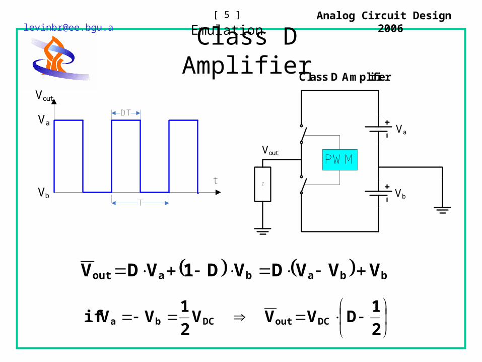
Class D Amplifier
outV
Z
aV
bV
PWM
bbabaout VVVDVD1VDV
aV
bVt
T
DT
outV
2
1DVVV
2
1VVif DCoutDCba
Class D Amplifier

[email protected] [6] Emulation Analog Circuit Design 2006
• Algorithm doesn’t handle with discontinuous function . Why?
• Tolerance less than 2 is inaccessible : Δy=2 is a constant
• Sign(0) is undefined
xsigny
x
Δy
1
-1
0
Convergence Problem

[email protected] [7] Emulation Analog Circuit Design 2006
• To find continuous differentiable and invertible function that behaves as sign (logic “ if ” function( .
• Proposed function : xx
xx
ee
eextanhy
xtanhy
x
1
-1
0
Convergence Problem Proposed Solution

[email protected] [8] Emulation Analog Circuit Design 2006
Convergence Problem Proposed Solution
• Increasing the slope
• Offset can be added
11050 6 xtanh.y
x
1
0
xtanhy 610
1110500 6 xtanh.

[email protected] [9] Emulation Analog Circuit Design 2006
Saw-tooth WaveVpulse Source
Td Tr PW Tf
PER
Tr Tf
PER
Vsw
TD = 1u
TF = {Tp/2}PW = 1uPER = {Tp}
V1 = -1
TR = {Tp/2}
V2 = 1
0
PARAMETERS:
Tp = {1/f}f = 500

[email protected] [10] Emulation Analog Circuit Design 2006
“Soft” PWM Simulation
302ms 304ms 306ms 308ms 310ms 312ms 314ms 315ms
5V
10V
15V
-1VSEL>>
V(E3:IN+) V(E3:IN-)-1.0V
0V
1.0VV(Ra:1,aa)
0V
5V
10V
15V
DriverDriver
E2
(tanh(1g* ( V(%IN+, %IN-) ) )+1 )*7.5
EVALUE
OUT+OUT-
IN+IN-
E3
(tanh(1g* ( V(%IN+, %IN-) ) ) +1)*7.5
EVALUE
OUT+OUT-
IN+IN-
Von=15 [V] Voff=0 [V]
v_ref
v_ref
ba
PWM Control Block
V3
TD = 1u
TF = {Tp/2}PW = 1uPER = {Tp}
V1 = -1
TR = {Tp/2}
V2 = 1
0
aabb
Ra
10
Rb
10
1VV10tanh7.5V SWref6
PWM
•SW – Saw-tooth Wave
•Ref – Reference Voltage

[email protected] [11] Emulation Analog Circuit Design 2006
Experimental CircuitDC Supply
inZ
aV
bV
PWM

[email protected] [12] Emulation Analog Circuit Design 2006
Equivalent Capacitor
Lω
1AC
Cω
1
j
1
Lω1A
1
j
1Z
2
veq
eqvin
μF5
1π502
11.5C
2eq

[email protected] [13] Emulation Analog Circuit Design 2006
Simulation Results : Av=1.5 , f=1k Ideal DC Supply
Time
600ms 605ms 610ms 615ms 620ms 625ms 630ms 635ms 640ms 645ms 650msI(current_sens) -0.5*cos(100*pi*time)
-1.0
0
1.0
SEL>>
V(high_in)-400V
0V
400V
Real Capacitor Current
Input Current
Input Voltage

[email protected] [14] Emulation Analog Circuit Design 2006
DC Voltage Supply
1:n
in
out
out
1:n
in
out
out
Rectifier with Transformer Isolation

[email protected] [15] Emulation Analog Circuit Design 2006
DC Voltage Supply
in
out
Voltage-Doubler Rectifier
C1
D2
C2D1
a out
in

[email protected] [16] Emulation Analog Circuit Design 2006
Voltage-Doubler Rectifier
C1
D2
C2D1Vin
a out
i
Vc1
Negative Half Cycle Positive Half Cycle
C1
D2
C2D1Vin
a out
i
Vc1
Vc2
in1c VV inc1c VVV 2Current flows if Current flows if
inc VV 22

[email protected] [17] Emulation Analog Circuit Design 2006
Experimental Circuit Self Supply
Class D Amplifier Voltage-Doubler Rectifier
PWM
Current limiter
inZ

[email protected] [18] Emulation Analog Circuit Design 2006
Self Supply PSpice Model
PARAMETERS:
Av = 1.5
Rr
5
C1{c}
C2{c}
C3{c}
C4{c}
(V(%IN) * {Av})
a
b
v_ref
R1639k
R21k
0
0
current_sens
0Vdc
Rp
20kRs
5 L
1H
1 2
D1MUR460
D3MUR460
D2MUR460
D4MUR460
M1
IRF840
M2
IRF840
aa
bb
V1
FREQ = 50VAMPL = 320
VOFF = 0
Class D Amplifier
Feedforward
Voltage Doubler Rectifier
current_sens_DC
0Vdc

[email protected] [19] Emulation Analog Circuit Design 2006
Simulation Results : Av=1.5 , f=1k
Time
600ms 605ms 610ms 615ms 620ms 625ms 630ms 635ms 640ms 645ms 650msI(current_sens) -0.5*cos(314*time)
-2.0
0
2.0
SEL>>
V(high_in)-400V
0V
400V
Real Capacitor Current
Input Current
Input Voltage

[email protected] [20] Emulation Analog Circuit Design 2006
Simulation Results : Av=1.5 , f=1k
Time
600ms 605ms 610ms 615ms 620ms 625ms 630ms 635ms 640ms 645ms 650msI(current_sens) -0.5*cos(314*time)
-2.0
0
2.0I(current_sens_DC)
-2.0A
0A
2.0A
SEL>>
Rectifier Current
Input Current
Real Capacitor Current
Rectifier Current Spikes

[email protected] [21] Emulation Analog Circuit Design 2006
Simulation Results : Av=1.5 , f=500
Time
600ms 605ms 610ms 615ms 620ms 625ms 630ms 635ms 640ms 645ms 650msI(current_sens) -0.5*cos(100*pi*time)
-1.0
0
1.0
SEL>>
I(current_sens_DC)
-1.0A
0A
1.0ARectifier Current
Input Current
Real Capacitor Current
Rectifier Current Spikes

[email protected] [22] Emulation Analog Circuit Design 2006
Simulation Results : Av=1.5 , f=10k
Rectifier Current Spikes
Time
600ms 605ms 610ms 615ms 620ms 625ms 630ms 635ms 640ms 645ms 650msI(current_sens) -0.5*cos(100*pi*time)
-2.0
0
2.0
SEL>>
I(current_sens_DC)
-2.0A
0A
2.0ARectifier Current
Input Current
Real Capacitor Current

[email protected] [23] Emulation Analog Circuit Design 2006
DC Voltage Supply
1:n
1:n
out
in
1:n
1:nout
Rectifier with Transformer Isolation

[email protected] [24] Emulation Analog Circuit Design 2006
Simulation Results : Av=1.5 , f=1k
Time
600ms 605ms 610ms 615ms 620ms 625ms 630ms 635ms 640ms 645ms 650msI(current_sens)
-2.0A
-1.0A
0A
1.0A
2.0A Voltage-Doubler Rectifier
Rectifier with Transformer Isolation
Input Current
Input Current
PSim Simulation

[email protected] [25] Emulation Analog Circuit Design 2006
Input Voltage Step Response 230 V rms to 460 V rms
Time
450ms 500ms 550ms 600ms 650ms 700msI(current_sens)
-20A
0A
20A
SEL>>
V(high_in)
-500V
0V
500V
Input Voltage
Input Current

[email protected] [26] Emulation Analog Circuit Design 2006
Power Dissipation
• Reactive Power
• Measured Energy Loss
VAr1202
0.75320Q
W7~

[email protected] [27] Emulation Analog Circuit Design 2006
Applications
• Compensator
• Gyrator
• Real Time High Power Variable Capacitor in Parametric Resonance Circuit

[email protected] [28] Emulation Analog Circuit Design 2006
Summary
• It can be seen that current has two current spikes in a period
• The reason of the current spikes is topology of the voltage – doubler rectifier
• The problem can be solved either improving the current topology or using another, more appropriated topology.

[email protected] [29] Emulation Analog Circuit Design 2006
Reference
• D.C. Hamill, M.T. Bina, The Bootstrap Variable Inductance and its
Applications in AC Power Systems, Applied Power Electronics
Conference and Exposition, 1999. APEC '99. Fourteenth Annual,
Volume 2, 14-18 March 1999 Page(s) : 896 - 902 vol.2

[email protected] [30] Emulation Analog Circuit Design 2006