elektronika ir elektrotechnika, 19(9): 75-80 emi...
TRANSCRIPT
http://www.diva-portal.org
This is the published version of a paper published in Elektronika ir Elektrotechnika.
Citation for the original published paper (version of record):
Majid, A., Saleem, J., Alam, F., Bertilsson, K. (2013)
EMI Suppression in High Frequency Half Bridge Converter.
Elektronika ir Elektrotechnika, 19(9): 75-80
http://dx.doi.org/10.5755/j01.eee.19.9.5653
Access to the published version may require subscription.
N.B. When citing this work, cite the original published paper.
Permanent link to this version:http://urn.kb.se/resolve?urn=urn:nbn:se:miun:diva-19737

ELEKTRONIKA IR ELEKTROTECHNIKA, ISSN 1392-1215, VOL. 19, NO. 9, 2013
Abstract—Electromagnetic effects influence the design of
power converters switching in MHz frequency region. In these
converters, the high switching frequency in combination with
sudden changes in current and voltage levels generate higher
order harmonics which causes Electro Magnetic Interference
(EMI). To study the effects of increased switching frequency on
conducted EMI, the harmonics amplitudes are analyzed by
increasing the switching frequency of a two wire input half
bridge power converter from 1.32 MHz to 3 MHz. In order to
suppress the Common Mode (CM) conducted EMI, different
possibilities of connecting the Y - capacitor in a two wire
universal input half bridge converter are discussed and the
conducted EMI is measured and analyzed by connecting the Y -
capacitor at different points. The line filters are designed,
characterized and implemented in order to suppress conducted
EMI. The effects of increased switching frequency on the line
filter design are studied by analysing the EMI spectrum of both
the converters. The analysis of results indicates that the filter
size is reduced by increasing the switching frequency of the
power converter.
Index Terms—Common mode, differential mode,
electromagnetic interference, electromagnetic compatibility,
line impedance stabilization network.
I. INTRODUCTION
With the development of emerging semiconductor
devices, such as the CoolMOS and GaN power MOSFETs,
high frequency multi-layered Printed Circuit Board (PCB)
and hybrid (POT +I) core power transformers it is possible
to design the high frequency (MHz range) and energy
efficient power converters [1]–[4]. Multi-resonant half
bridge converters have been designed in the 1 MHz – 4 MHz
switching frequency range, up-to a 40 W output power level
and with 92 % energy efficiency. Planar power transformers
used in these converters are highly energy efficient and ultra-
compact [4]. The motivation for designing these high
frequency converters is that the majority of the power
electronic devices used are surface mounted. These devices
have reduced parasitic components as compared to those for
the through-hole devices and closer placement of the
components has thus become possible. Therefore, surface
mounted devices are better from an EMI point of view as
Manuscript received February 19, 2013; accepted May 28, 2013.
compared to through-hole devices.
The energy efficiency of power converters is an important
parameter. However, because of very stringent
Electromagnetic Compatibility (EMC) regulations such as
International Special Committee on Radio Interference
(CISPR) and Federal Communication Commission (FCC)
etc., it has also become a compulsory requirement and it is
as important as the energy efficiency. The EMI produced by
the power converters is of a broadband nature (from
operating frequency to GHz range). The conducted
electromagnetic signals travel within the circuit as well as on
power lines [5]. Therefore, careful design of the power
stages of these converters is inevitable for the EMI
reduction. In addition to soft switching and filtering different
spread spectrum techniques are also helpful for the reduction
of EMI in the power converters [6].
In isolated power converters, the major sources of
Common Mode (CM) noise are charging and discharging of
parasitic capacitances, mainly the heat sink and transformer
inter-winding capacitance [7], [8]. The inter-winding
capacitances of a power transformer reduce the high
frequency AC isolation and result in common-mode
currents. The return current path at high switching frequency
is highly critical with regards to the EMC performance of a
power converter.
The leakage inductance of the power transformer is also
an extremely critical parasitic element. At higher switching
frequencies, it resonates with inter-winding capacitance and
provides a low impedance path for the CM EMI. Therefore,
this results in high frequency CM noise peaks. The leakage
inductance may also resonate with the junction capacitance
of the rectifier diode. It can thus become a source of high
frequency CM noise on the secondary side [9].
The Differential Mode (DM) noise is mainly caused by
the magnetic coupling Ldi/dt. The DM current generated at
the input of the device under test is measured as an
interference voltage across the load impedance of each line
with respect to the ground [10].
In [11] the author has performed the initial measurements
and analysis of the conducted EMI in DC-DC power
converters, switching at 3.45 MHz and at a power level of
6 W. The Line Impedance Stabilization Network (LISN) was
designed and implemented for EMI measurements. The
EMI Suppression in High Frequency Half
Bridge Converter
A. Majid1, J. Saleem1, F. Alam2, K. Bertilsson1 1Department of Information Technology and Media, Mid Sweden University,
Holmgatan 10, 851 70 Sundsvall, Sweden 2SEPS Technologies AB,
Holmgatan 10, 851 70 Sundsvall, Sweden
http://dx.doi.org/10.5755/j01.eee.19.9.5653
75

ELEKTRONIKA IR ELEKTROTECHNIKA, ISSN 1392-1215, VOL. 19, NO. 9, 2013
design, implementation and characterization of the EMI
filter and the measurement of the suppressed conducted
noise by applying the filter were discussed.
In this paper, the conducted EMI analysis of two high
frequency half bridge AC DC power converters switching is
presented. Both converters have same output power level of
20 W. One converter is switching at 1.32 MHz and the other
is switching at 3 MHz. Their conducted EMI is measured
using a HAMEG HMS3000 spectrum analyzer and a
HAMEG HM6050-2 LISN. Different possibilities for the
suppression of conducted EMI are investigated. Two wire
input line filters are designed and implemented for both
power converters. The EMI spectrum is analyzed with and
without the application of filter. The remainder of this paper
is organized as follows:
In Section II, the high frequency half bridge converter
used for the conducted EMI measurement is briefly
described;
In Section III, the EMI measurement results without
application of filter are discussed;
In Section IV, the techniques for reducing the conducted
EMI in two input off-line power supplies are discussed
and the harmonics amplitude after adding CY capacitor
between different points is analyzed;
In Section V, the design, implementation and
characterization of the line filter are discussed;
In Section VI, the measurement results obtained from the
application of the EMI filter are discussed and a
comparison of the harmonic amplitude with and without
filter is presented.
II. HIGH FREQUENCY HALF BRIDGE CONVERTER
A multi-resonant AC-DC half bridge converter is selected
for the conducted EMI measurements. In these emerging
power converters, Zero Voltage Switching (ZVS) is
achieved for the entire load range using a hybrid planar
power transformer and GaN power MOSFETs. The energy
efficiency, the design details of the converter and the power
transformer used for the EMI measurement are given in
references [3], [4]. A hybrid core centre tapped planar power
transformer with a 0.3 mm air gap in the POT core centre
post is used in the half bridge converter [4].
The smaller values of the inter-winding capacitance
(i.e, 22.2 pF) and the secondary side leakage inductance
(28 nH) [4], of these power transformers are helpful with
regards to reduction of the CM noise current flowing
through the inter-winding capacitance. These high frequency
power transformers are less vulnerable to CM conducted
EMI. However, it is important to analyze the radiated EMI
due to the resonance of the leakage inductance with the
inter-winding capacitance and the junction capacitance of
the rectifier diode for these high frequency power
converters.
III. EMI MEASUREMENTS OF HALF BRIDGE CONVERTER
The conducted EMI of both the half bridge converters is
measured according to CISPR (EN 55022 Class B
QPEAK) [10] requirements. The frequency spectrum of
conducted EMI, in case of half bridge converter switching at
1.32 MHz, is shown in Fig. 1(a).
10-1
100
101
102
20
30
40
50
60
70
80
90
100
110
120
Frequency (MHz)
Le
ve
l (
dB
uV
)
Peak
EN 55022 Class B QPEAK
a)
10-1
100
101
102
20
30
40
50
60
70
80
90
100
110
120
Frequency (MHz)
Level
(dB
uV
)
Peak
EN 55022 Class B QPEAK
b)
Fig. 1. Conducted EMI spectrum: a – 1.32 MHz; b – 3 MHz converter.
The spectrum is comprised of both even and odd order
harmonics. The fundamental frequency component is at
91.38 dBµV, which is 35.38 dB above the CISPR limit. The
third and fifth order harmonics are at 90 dBµV. The other
higher order harmonics are approximately 80 dBµV –
85 dBµV. It is observed that all the harmonics are above the
CISPR limit and thus the converter does not meet the
regulatory requirement.
In order to analyze the effect of an increased switching
frequency on the harmonic amplitude, the switching
frequency of the converter is increased from 1.32 MHz to
3 MHz. The conducted EMI spectrum for a 3 MHz
converter is shown in Fig. 1(b). From measurement results it
is observed that the fundamental frequency component is at
93 BµV, the third and fifth order harmonics is at 96.4 dBµV
and other higher order harmonics are at approximately
90 dBµV. The harmonics amplitude (especially fundament,
third and fifth harmonics) of this converter are higher than
that of 1.32 MHz power converter because of increased
switching frequency.
IV. EFFECT OF ADDING CY CAPACITOR
In order to suppress the conducted EMI, a commonly used
topology is a three pin line filter. These filters consist of CM
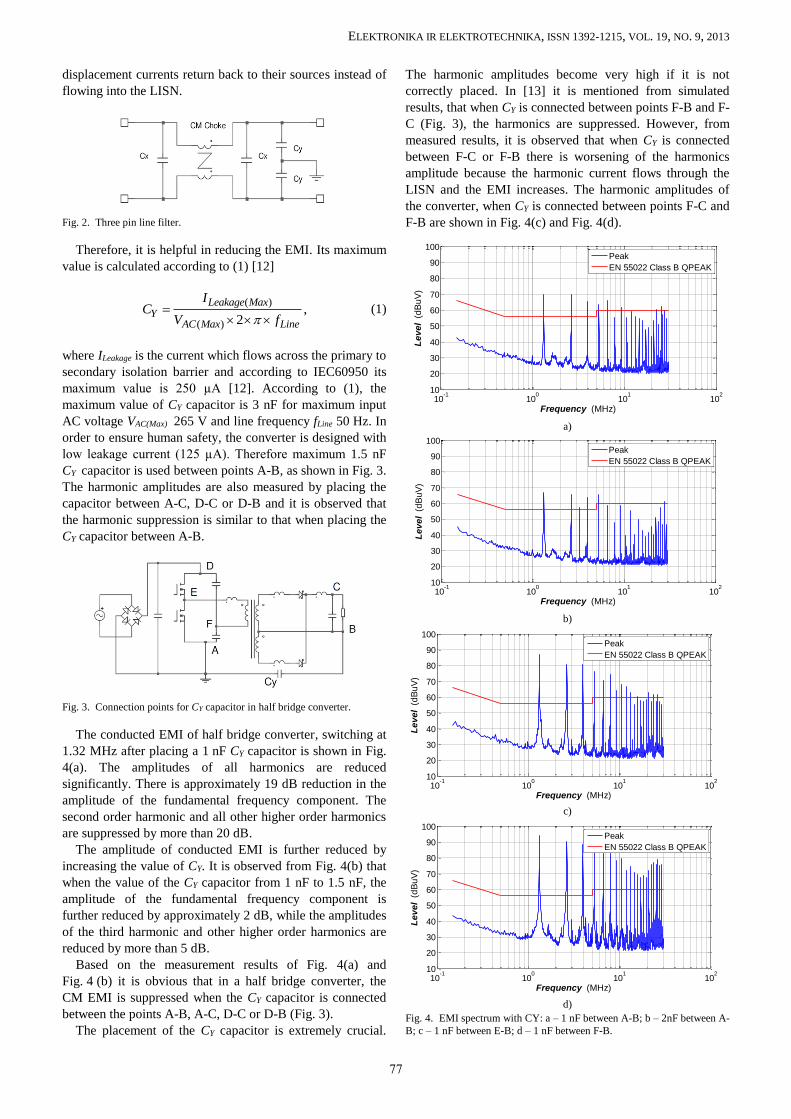
chokes, CX and CY capacitors as shown in Fig. 2.
The majority of the modern power supplies have two pin
input (without safety ground) connectors. In the two wires
universal input power supplies, a CY capacitor is placed
between the primary and secondary ground of the power
transformer instead of placing it in the line filter.
With the placement of the CY capacitor, most of the
76
ELEKTRONIKA IR ELEKTROTECHNIKA, ISSN 1392-1215, VOL. 19, NO. 9, 2013
displacement currents return back to their sources instead of
flowing into the LISN.
Fig. 2. Three pin line filter.
Therefore, it is helpful in reducing the EMI. Its maximum
value is calculated according to (1) [12]
( )
( )
,2
Leakage MaxY
AC Max Line
IC
V f
(1)
where ILeakage is the current which flows across the primary to
secondary isolation barrier and according to IEC60950 its
maximum value is 250 µA [12]. According to (1), the
maximum value of CY capacitor is 3 nF for maximum input
AC voltage VAC(Max) 265 V and line frequency fLine 50 Hz. In
order to ensure human safety, the converter is designed with
low leakage current (125 µA). Therefore maximum 1.5 nF
CY capacitor is used between points A-B, as shown in Fig. 3.
The harmonic amplitudes are also measured by placing the
capacitor between A-C, D-C or D-B and it is observed that
the harmonic suppression is similar to that when placing the
CY capacitor between A-B.
Fig. 3. Connection points for CY capacitor in half bridge converter.
The conducted EMI of half bridge converter, switching at
1.32 MHz after placing a 1 nF CY capacitor is shown in Fig.
4(a). The amplitudes of all harmonics are reduced
significantly. There is approximately 19 dB reduction in the
amplitude of the fundamental frequency component. The
second order harmonic and all other higher order harmonics
are suppressed by more than 20 dB.
The amplitude of conducted EMI is further reduced by
increasing the value of CY. It is observed from Fig. 4(b) that
when the value of the CY capacitor from 1 nF to 1.5 nF, the
amplitude of the fundamental frequency component is
further reduced by approximately 2 dB, while the amplitudes
of the third harmonic and other higher order harmonics are
reduced by more than 5 dB.
Based on the measurement results of Fig. 4(a) and
Fig. 4 (b) it is obvious that in a half bridge converter, the
CM EMI is suppressed when the CY capacitor is connected
between the points A-B, A-C, D-C or D-B (Fig. 3).
The placement of the CY capacitor is extremely crucial.
The harmonic amplitudes become very high if it is not
correctly placed. In [13] it is mentioned from simulated
results, that when CY is connected between points F-B and F-
C (Fig. 3), the harmonics are suppressed. However, from
measured results, it is observed that when CY is connected
between F-C or F-B there is worsening of the harmonics
amplitude because the harmonic current flows through the
LISN and the EMI increases. The harmonic amplitudes of
the converter, when CY is connected between points F-C and
F-B are shown in Fig. 4(c) and Fig. 4(d).
10-1
100
101
102
10
20
30
40
50
60
70
80
90
100
Frequency (MHz)L
ev
el (
dB
uV
)
Peak
EN 55022 Class B QPEAK
a)
10-1
100
101
102
10
20
30
40
50
60
70
80
90
100
Frequency (MHz)
Le
ve
l (
dB
uV
)
Peak
EN 55022 Class B QPEAK
b)
10-1
100
101
102
10
20
30
40
50
60
70
80
90
100
Frequency (MHz)
Le
ve
l (
dB
uV
)
Peak
EN 55022 Class B QPEAK
c)
10-1
100
101
102
10
20
30
40
50
60
70
80
90
100
Frequency (MHz)
Le
ve
l (
dB
uV
)
Peak
EN 55022 Class B QPEAK
d)
Fig. 4. EMI spectrum with CY: a – 1 nF between A-B; b – 2nF between A-
B; c – 1 nF between E-B; d – 1 nF between F-B.
77

ELEKTRONIKA IR ELEKTROTECHNIKA, ISSN 1392-1215, VOL. 19, NO. 9, 2013
The conducted EMI of the 3 MHz half bridge converter
after placing a 1.5 nF CY between A-B points is shown in
Fig. 5. In this case the fundamental frequency component is
suppressed by 26 dB, the second order harmonic is
suppressed by 10 dB while other higher order harmonics are
suppressed by more than 25 dB.
10-1
100
101
102
20
30
40
50
60
70
80
90
100
110
120
Frequency (MHz)
Level
(dB
uV
)
Peak
EN 55022 Class B QPEAK
Fig. 5. Frequency spectrum of EMI with the addition of 1.5 nF CY.
V. EMI FILTER DESIGN AND IMPLEMENTATION
From the measurement results shown in Section IV, it can
be observed that a significant reduction in the conducted
EMI is achieved by the placement of the CY capacitor. The
amplitudes of the harmonics are still higher than the CISPR
limit. Therefore, in order to further reduce the conducted
EMI of the power converter, a line filter is required to
suppress fundamental frequency component as well as
higher order harmonics up to 30 MHz.
In relation to the design for a line filter, the requirement is
that no undesired signal should reach the external 100 Ω
radiation impedance. Therefore, the series components (CM
choke in this design) must have an impedance which is
significantly higher than 100 Ω and that the parallel
components (X capacitors in this design) must have an
impedance which is significantly less than 100 Ω over the
desired frequency range [14].
In two wire input offline power supplies, the line filter
consists of only line and neutral connections and does not
have safety ground connection. The filter circuit is
comprised of CM chokes and X capacitors. The commonly
used EMI filter topologies are designed to attenuate the high
frequency conducted noise and include LC low pass filters.
To attenuate a particular frequency, band reject filters may
also be used.
Various parasitic elements exist in the filter such as
parasitic inductance of capacitors, the parasitic capacitance
of inductors and the parasitic parameters of the PCB trace,
which cannot be determined by means of measurements.
Therefore the real high frequency characteristic of the EM1
filter will be much different from its expected value and the
two identical filters may behave differently [15]. The
electromagnetic couplings among the filter components and
circuit layouts also affect the high frequency performance of
the EMI filters [16].
With regards to the selection of filter components, it is
important to consider the CM chokes core material, DC
resistance and the capacitors dielectric material. The CM
choke with a higher DC resistance has a deleterious effect on
the energy efficiency of the power converter. The effect of
the DC resistance on the energy efficiency of the input filter
is analyzed by taking measurements with an AC input
voltage of 100 V and different output power levels. A
summary of the measurements is given in Table I.
The schematic diagrams of the filter designed for the
1.32 MHz and 3 MHz converters are shown in Fig. 6(a) and
Fig. 6(b) respectively. The fundamental frequency
component in the 3 MHz converter is at a frequency which is
approximately 2.3 times higher than that for 1.32 MHz
converter and, thus the size of the filter components is
reduced.
TABLE I. POWER CONVERSION EFFICIENCY OF THE INPUT
FILTER.
Input
Power
(W)
Energy efficiency (Percentage)
Bridge
Rectifier and
hold-up
capacitors
Bridge Rectifier, hold-up capacitors and
Line Filter
CM choke
DCR
50 mΩ
CM choke
DCR
540 mΩ
CM choke
DCR
700 mΩ
20 98.0 97.4 97.3 97.0
30 97.9 97.4 96.9 96.7
40 97.7 97.3 96.7 96.4
50 97.6 97.1 96.4 96.2
a)
b)
Fig. 6. Filter schematic for: a – 1.3 MHz; b – 3 MHz converter.
In the line filter datasheets, the attenuation plots are given
by assuming that both noise source and load have 50 Ω
impedances. However, in the actual circuit measurements,
the noise source impedance (device under test) deviates from
the noise load impedance (LISN). When the impedance
difference of the noise source and the noise load is more
significant, then the attenuation of the 50 Ω and non 50 Ω
system becomes significant. Therefore, it is necessary to
characterize the filter for its performance prediction [17].
The parasitic extraction and insertion loss of EMI filters can
be calculated by using scattering parameters (S-parameters).
The insertion voltage gain, with measured S-parameters
(S11, S12, S21 and S22), arbitrary source impedance ZS and load
impedance ZL is calculated by using (2) [18]. The scattering
parameters are measured both for the CM and DM EMI
filters using a network analyzer.
12
11 22 12 21
(1 ),
(1 )(1 )
L SV
S L S L
SA
S S S S
(2)
where ΓS is source side reflection coefficient and ΓL is load
78

ELEKTRONIKA IR ELEKTROTECHNIKA, ISSN 1392-1215, VOL. 19, NO. 9, 2013
side reflection coefficient as given in (3) and (4)
respectively. Z0 is the characteristic impedance, which is
usually 50 Ω:
0
0
,SS
S
Z Z
Z Z
(3)
0
0
.LL
L
Z Z
Z Z
(4)
For the CM filter, the insertion loss is calculated by using
the arbitrary values, ZS = 1 MΩ and ZL = 25 Ω and for the
DM filter by using the arbitrary values of ZS = 1 MΩ and
ZL = 100 Ω [18]. The insertion voltage gain for the filter
shown in Fig. 6(a) is plotted in Fig. 7(a) and for the filter
shown in Fig. 6(b) is plotted in Fig. 7(b).
100
101
102
-35
-30
-25
-20
-15
-10
-5
0
Frequency (MHz)
Ins
ert
ion
Vo
lta
ge
Ga
in
(dB
)
CM insertion loss
DM insertion loss
a)
100
101
102
-35
-30
-25
-20
-15
-10
-5
0
Frequency (MHz)
Ins
ert
ion
Vo
lta
ge
Ga
in
(dB
)
CM insertion loss
DM insertion loss
b)
Fig. 7. Line filter insertion loss: a – 1.32 MHz; b – 3 MHz power
converter.
VI. EMI MEASUREMENTS AFTER FILTER APPLICATION
The two stage filter explained in Section V is designed
and implemented to suppress the conducted EMI of both
power converters. The EMI plot of 1.32 MHz half bridge
converter after the application of a line filter is shown in
Fig. 8(a).
10-1
100
101
102
20
30
40
50
60
70
80
90
100
110
120
Frequency (MHz)
Le
ve
l (
dB
uV
)
Peak
EN 55022 Class B QPEAK
a)
10-1
100
101
102
20
30
40
50
60
70
80
90
100
110
120
Frequency (MHz)
Level
(dB
uV
)
Peak
EN 55022 Class B QPEAK
b)
Fig. 8. EMI plot after using filter: a – 1.32 MHz; b – 3 MHz converter.
10-1
100
101
102
0
20
40
60
80
100
120
140
Frequency (MHz)
Harm
on
ics A
mp
litu
de (dB
uV
)
EN 55022 Class B QPEAK
Without filter and Cy
Without filter, Cy-1.5nF
With filter, Cy-1.5nF
a)
10-1
100
101
102
0
20
40
60
80
100
120
140
Frequency (MHz)
Harm
on
ics A
mp
litu
de (dB
uV
)
EN 55022 Class B QPEAK
Without filter and Cy
Without filter, Cy-1.5nF
With filter, Cy-1.5nF
b)
Fig. 9. Harmonic amplitude comparison: a – 1.32 MHz, b – 3 MHz
converter.
It is obvious from the plot that the fundamental frequency
component is further reduced by 15 dB after the application
of the filter. The fundamental frequency component and the
third harmonic fall below the CISPR limit, while all other
harmonics are more than 10 dB below the limit (more
suppressed than the fundamental frequency component and
third harmonic). The comparison of the harmonic amplitudes
for 1.32 MHz half bridge converter without filter, with
addition of CY and with two stage input line filter shown in
Fig. 6(a) is plotted in Fig. 9(a). Form the harmonics
comparison plot it is obvious that the proper placement of a
CY capacitor and a two stage line filter are required to
suppress the conducted EMI below the CISPR limit.
In order to keep the harmonics amplitudes in the 3 MHz
power converter, below CISPR limit a two stage filter, as
shown in Fig. 6(b) is applied and the measurement results
are shown in Fig. 8(b). It is observed that the fundamental
frequency component is further suppressed by 21 dB with
the addition of the line filter. The comparison of the
harmonic amplitudes for the half bridge converter switching
at 3 MHz, before after the application of the line filter, is
79

ELEKTRONIKA IR ELEKTROTECHNIKA, ISSN 1392-1215, VOL. 19, NO. 9, 2013
plotted in Fig. 9(b). It is observed that after the application
of the line filter, all the harmonics fall below the CISPR
limit.
From the measurement results of both the converter
circuits, it is observed that although the harmonics
amplitudes of 3 MHz half bridge converter are slightly
higher than that of 1.32 MHz converter but the 3 MHz
converter requires smaller EMI filter. Therefore, the overall
size of the converter can be reduced by increasing the
switching frequency.
VII. CONCLUSIONS
The focus of this paper is to measure, analyze and
suppress the conducted EMI for emerging power converters
switching in the MHz frequency range and to observe the
effects of this increased switching frequency on the filter
design. The conducted EMI is measured by connecting a CY
capacitor at various points in the half bridge converter.
Based on measurement results, the proper connection points
for Y capacitor in a half bridge converter are suggested and
it is concluded that a properly connected Y capacitor is
useful for the suppression of CM conducted EMI, while the
improperly connected Y capacitor results in increased EMI.
The energy efficiency of the input filter is measured for
different output power levels and it is observed that if DC
resistance of common modes changes from 50 mΩ to
700 mΩ, then the energy efficiency of the input filter is
degraded by approximately 1 %. It is concluded that the size
of the filter components is reduced for converter switching at
3 MHz. This is a motivating factor for designing the power
converters at higher switching frequencies.
REFERENCES
[1] H. B. Kotte, “High Speed (MHz) Switch Mode Power
Supplies(SMPS) using Multilayered Coreless PCB Transformer
technology Passive gate drive circuit using Coreless Printed Circuit
Board (PCB) Signal Transformer”, Licentiate Thesis 62, Mid Sweden
University.
[2] R. Ambatipudi, “Multilayered Coreless Printed Circuit Board (PCB)
Step-down Transformers for High Frequency Switch Mode Power
Supplies (SMPS)”, Licentiate Thesis 61, Mid Sweden University.
[3] H. B. Kotte, R. Ambatipudi, K. Bertilsson, “High speed series
resonant converter (SRC) using multilayered coreless printed circuit
board (PCB) step-down power transformer”, in Proc. of EEE 33rd
Int. Telecommunications Energy Conf. (INTELEC 2011), 2011,
pp. 1–9. [Online]. Available: http://dx.doi.org/10.1109/
INTLEC.2011.6099785
[4] H. B. Kotte, R. Ambatipudi, K. Bertilsson, “Effect of Air Gap on the
Performance of Hybrid Planar Power Transformer in High Frequency
(MHz) Switch Mode Power Supplies (SMPS)”, in Proc. of Coil
Winding, Insulation and Electrical Manufacturing Int. Conf. and
Exhibition (CWIEME), Berlin, Germany, 2012.
[5] M. H. Rashid, Electronics Handbook: Devices, Circuits, and
Applications, 3rd ed., pp 1103–1104.
[6] J. Jankovskis, D. Stepins, S. Tjukovs, D. Pikulins, “Examination of
Different Spread Spectrum Techniques for EMI Suppression in dc/dc
Converters”, Elektronika ir Elektrotechnika (Electronics and
Electrical Engineering), no. 6, pp. 60–64, 2008.
[7] R. Redl, “Power electronics and electromagnetic compatibility”, in
Proc. of 27th Annual IEEE Power Electronics Specialists Conf.,
(PESC 96), 1996, pp.15–21.
[8] M. T. Zhang, “Electrical Thermal and EMI Designs of High Density
Low Profile Power Supplies ELECTRICAL”, Ph.D. dissertation
Virginia Polyt. Inst. and State Univ., 1997.
[9] P. Kong, F. C. Lee, “Transformer structure and its effects on common
mode EMI noise in isolated power converters”, in Proc. of 25th
Annual IEEE Applied Power Electronics Conf. and Exposition
(APEC 2010), 2010, pp.1424–1429. [Online]. Available:
http://dx.doi.org/10.1109/APEC.2010.5433416
[10] T. William, EMC for Product Designers, 4th ed.
[11] A. Majid, J. Saleem, H. B. Kotte, R. Ambatipudi, K. Bertilsson,
“Design and implementation of EMI filter for high frequency (MHz)
power converters”, in Proc. of Int. Symposium on Electromagnetic
Compatibility (EMC EUROPE), 2012, pp.1–4. [Online]. Available:
http://dx.doi.org/10.1109/EMCEurope.2012.6396738
[12] P. Vauhan, “Designing low leakage current supplies”, [Online].
Available: http://www.eetasia.com/ARTICLES/2004NOV/B/2004NO
V16_POW_TA.pdf
[13] H. I. Hsieh, L. Huwang, T. C. Lin, D. Chen, “Use of a Common-
Mode Capacitor in Two-Wire and Three-Wire Offline Power
Supplies”, IEEE Trans. Industrial Electronics, vol. 55, no. 3, pp.
1435–1443, Mar. 2008. [Online]. Available:
http://dx.doi.org/10.1109/TIE.2007.896263
[14] B. R. Archambeault, “PCB Design for Real World EMI Control”,
Kluwer Academic Publishers, 2004, pp. 151–153.
[15] D. H. Liu, J. G. Jiang, “High frequency characteristic analysis of EMI
filter in switch mode power supply (SMPS)”, in Proc. of IEEE 33rd
Annual Power Electronics Specialists Conf., 2002, vol. 4, pp. 2039–
2043.
[16] S. Wang, F. C. Lee, D. Y. Chen, W. G. Odendaal, “Effects of
parasitic parameters on EMI filter performance”, IEEE Trans. Power
Electronics, vol. 19, no. 3, pp. 869–877, May 2004. [Online].
Available: http://dx.doi.org/10.1109/TPEL.2004.826527
[17] D. Zhang, D. Y. Chen, D. Sable, “A New Method to Characterize
EM1 Filter”, in Proc. of IEEE Applied Power Electronics Conf. &
Exposition Anaheim, CA, 1998, pp. 929–933.
[18] S. Wang, F. C. Lee, D. Y. Chen, W. G. Odendaal, “Characterization
and parasitic extraction of EMI filters using scattering parameters”,
IEEE Trans. Power Electronics, vol. 20, no. 2, pp. 502–510, Mar.
2005. [Online]. Available: http://dx.doi.org/10.1109/
TPEL.2004.842949
80