electron and phonon properties of graphene: their ... · electron and phonon properties of graphene...
TRANSCRIPT
Electron and Phonon Properties of Graphene:Their Relationship with Carbon Nanotubes
J.-C. Charlier1, P. C. Eklund2 J. Zhu2, A. C. Ferrari3
1 Unite de Physico-Chimie et de Physique des MateriauxUniversite Catholique de Louvain1 Place Croix du Sud, 1348 Louvain-la-Neuve, [email protected]
2 Department of Physics, The Pennsylvania State University104 Davey Lab, University Park, PA 16802-6300, [email protected], [email protected]
3 Engineering Department, Cambridge University9 JJ Thomson Avenue, Cambridge CB3 OFA, [email protected]
Abstract. The discovery of Novoselov et al. (2004) of a simple method to transfera single atomic layer of carbon from the c-face of graphite to a substrate suitablefor the measurement of its electrical and optical properties has led to a renewed in-terest in what was considered to be before that time a prototypical, yet theoretical,two-dimensional system. Indeed, recent theoretical studies of graphene reveal thatthe linear electronic band dispersion near the Brillouin zone corners gives rise toelectrons and holes that propagate as if they were massless fermions and anomalousquantum transport was experimentally observed. Recent calculations and experi-mental determination of the optical phonons of graphene reveal Kohn anomaliesat high-symmetry points in the Brillouin zone. They also show that the Born–Oppenheimer principle breaks down for doped graphene. Since a carbon nanotubecan be viewed as a rolled-up sheet of graphene, these recent theoretical and exper-imental results on graphene should be important to researchers working on carbonnanotubes. The goal of this contribution is to review the exciting news about theelectronic and phonon states of graphene and to suggest how these discoveries helpunderstand the properties of carbon nanotubes.
1 Introduction
The fundamental building block of both a graphite crystal and a carbon nano-tube is the graphene layer shown schematically in Fig. 1a. Such an atomicstructure is characterized by two types of C–C bonds (σ, π) constructed fromthe four valence orbitals (2s, 2px, 2py, 2pz), where the z-direction is perpen-dicular to the sheet. Three σ-bonds join a C atom to its three neighbors.They are quite strong, leading to optical-phonon frequencies much higherthan observed in diamond. In addition, the C–C bonding is enhanced by afourth bond associated with the overlap of pz (or π) orbitals. Graphite iscomprised of coherently stacked layers of graphene. Two layers (A and B)are needed to define the unit cell in graphite. The three-dimensional (3D)A. Jorio, G. Dresselhaus, M. S. Dresselhaus (Eds.): Carbon Nanotubes,Topics Appl. Physics 111, 673–709 (2008)
Springer-Verlag Berlin Heidelberg 2008

674 J.-C. Charlier et al.
structure of graphite is therefore held together by a weak interlayer van derWaals (vdW) force. A single-wall carbon nanotube (SWNT), on the otherhand, is a seamless cylinder of graphene. SWNTs are analogously bound ina bundle by the vdW force. The electronic properties of graphene, graphiteand carbon nanotubes are determined by the bonding π- and antibonding π∗-orbitals that form wide electronic valence and conduction bands (Fig. 1b). Asthe tube diameter decreases, the bond angle between the σ and π orbitals in-creases slightly, introducing curvature effects into the electronic and phononproperties of SWNTs.
Theoretical calculations show that the π-band overlap in graphite disap-pears as the layers are further separated over their equilibrium distance ingraphite. This leads to decoupled graphene layers that can be described as azero-gap semiconductor. The π-band electronic dispersion for graphene nearthe six corners of the 2D hexagonal Brillouin zone is found to be linear. Thus,“cones” of carriers (holes and electrons) appear in the corners of a 2D Bril-louin zone whose points touch at the Fermi energy, as shown in Fig. 1c. Thelinear electronic band dispersion leads to the term “massless Dirac fermions”for these carriers. The six points where the cones touch are referred to as the“Dirac” points in the graphene literature.
Graphene, because of its structural simplicity (two atoms per unit cell),has been extensively investigated in theory for the past 60 years [1]. How-ever, only recently has it been possible to produce ultrathin films containinga countable number (n) of graphene layers (i.e., 1 < n < 20). The synthetictechniques fall into two categories. The first approach exploits the weak bond-ing between the graphene layers by pealing off an n-graphene layer (nGL) bychemical means [2–6] or by mechanical means [7, 8]. Mechanical separationof nGLs from the parent crystal involves rubbing the freshly cleaved quasi-2D system against a smooth substrate. This technique has allowed grapheneand nGLs to be studied in the laboratory for the first time [7]. It is simple,inexpensive and produces graphene and nGL flakes of very high quality. How-ever, this approach lacks the scalability required by mass device production.The second approach grows epitaxial graphitic films by thermal decomposi-tion of SiC [9–12]. This technique has the potential of producing large-arealithography-compatible films and is rapidly advancing at the moment.
In this contribution, we review the connection between the electron andphonon states in graphene (nGLs) and SWNTs. We begin with a discussionof the electronic states. Recent theoretical arguments and experiments areconverging on a picture of free carriers in graphene near the Fermi energybehaving as massless Dirac fermions propagating at ∼ 1/100 the speed oflight, i.e., they do not behave as simple electrons or holes with an effec-tive mass. Experimental observations of an anomalous integer quantum Halleffect in graphene has been reported recently and has created a lot of atten-tion [13, 14]. These and other interesting experimental electronic transportresults are reviewed as well [15] with further discussion provided in the con-tributions in this volume by Ando and by Spataru et al. We then discuss

Electron and Phonon Properties of Graphene 675
Fig. 1. Illustration of the carbon valence orbitals. (a) The three inplane σ (s, px, py)orbitals in graphene and the π (pz) orbital perpendicular to the sheet. The inplaneσ and the π bonds in the carbon hexagonal network strongly connect the carbonatoms and are responsible for the large binding energy and the elastic propertiesof the graphene sheet. The π orbitals are perpendicular to the surface of the sheet.The corresponding bonding and the antibonding σ bands are separated by a largeenergy gap of ∼ 12 eV (b), while the bonding and antibonding π states lie in thevicinity of the Fermi level (EF). Consequently, the σ bonds are frequently neglectedfor the prediction of the electronic properties of graphene around the Fermi energy.Dirac cones located at the six corners of the 2D Brillouin zone are illustrated in (c)
the optical phonons in graphene that are directly accessible by Raman spec-troscopy and give rise to the most prominent Raman peaks when graphene isfolded into nanotubes. We focus on their coupling to electrons, which is keyto understanding many phenomena in graphene and nanotubes.
For example, it was recently argued that in doped graphene, the adia-batic Born–Oppenheimer approximation [16], valid in many solid-state sys-tems, breaks down [17]. The electron–phonon interaction in graphene hasalso been carefully re-examined and has been recently shown to give rise toKohn anomalies in the phonon dispersion at important points (Γ , K) in theBrillouin zone where the phonons can be studied by Raman spectroscopy [18–21]. Many of these new ideas proposed for graphene and nGLs carry over tonanotubes. Kohn anomalies are responsible for the different Raman spectra ofmetallic and semiconducting nanotubes, and non-Born–Oppenheimer effectsstrongly shape the Raman spectra of doped and annealed nanotubes [19, 22].These connections are also discussed in this review.
2 Electronic Properties and Transport Measurements
2.1 Graphene
2.1.1 Electronic Band Structure
Figure 2 shows the ab-initio calculations of the electronic bands of graphenealong the high-symmetry M–Γ–K directions [23]. Its space group (P3m)

676 J.-C. Charlier et al.
contains a mirror-plane symmetry, allowing symmetric σ and antisymmetricπ states to be distinguishable. In a 2D crystal, a parallel mirror symmetryoperation separates the eigenstates for the whole Brillouin zone, and not onlyalong some high-symmetry axis. The π and π∗ bands touch at the corners ofthe hexagonal Brillouin zone. Such corners are labeled by their momentumvector usually denoted by K and K ′. Consequently, graphene is a specialsemimetal or zero-gap semiconductor, whose intrinsic Fermi surface is reducedto the six points at the corners of the 2D hexagonal Brillouin zone. Close tothe Fermi energy, the π and π∗ bands are quasilinear (linear very close toK, K ′) (Fig. 1c), in contrast with the usual quadratic energy–momentumrelation obeyed by electrons at band edges in conventional semiconductors.When several interacting graphene planes are stacked, as in nGLs or in aperfect graphite crystal, the former antisymmetric π bands are split (owingto bonding or antibonding patterns), whereas the σ bands are much lessaffected by the stacking.
The graphene sheet is thus highly specific for this linear energy–momentumrelation. The electronic group velocity, estimated at the Dirac points, is quitehigh: ∼ 1×10⁶ m/s. Consequently, graphene exhibits electronic properties fora 2D gas of charged particles described by an equation of the form of the rel-ativistic Dirac equation rather than the nonrelativistic Schrodinger equationwith an effective mass. Indeed, in graphene, charge carriers mimic particleswith zero mass and an effective “speed of light” c∗ ∼ 1 × 10⁶ m/s. Recently,graphene has revealed a variety of unusual transport phenomena characteris-tic of two-dimensional Dirac fermions, such as an anomalous integer quantumHall effect, a “minimum” conductivity of order 4e2/h even when the carrierconcentration tends to zero, a cyclotron mass mc of massless carriers with anenergy E described by E = mcc
∗2, and Shubnikov–de Haas oscillations thatexhibit a phase shift of π due to Berry’s phase [13, 14]. These remarkableproperties will be described in the next section.
The electronic structure of graphene can be reasonably well described us-ing a rather simple tight-binding Hamiltonian, leading to analytical solutionsfor their energy dispersion and related eigenstates [23]. Since the bondingand antibonding σ bands are well separated in energy (> 10 eV at Γ ), theyare frequently neglected in semiempirical calculations since they are too faraway from the Fermi level to play a role. Only the remaining two π bandsare thus needed to describe the electronic properties of graphene.
When the atoms are placed onto the graphene hexagonal lattice (Fig. 1a),the electronic wavefunctions from different atoms overlap. However, such anoverlap between the pz(π) orbitals and the s or the px and py orbitals isstrictly zero by symmetry. Consequently, the pz electrons, which form the πbands in graphene, can be treated independently from the other valence elec-trons. Within this π-band approximation, it is easy to describe the electronic

Electron and Phonon Properties of Graphene 677
Fig. 2. (a) Electronic band structure of graphene from ab-initio calculations [23].The bonding σ and the antibonding σ∗ bands are separated by a large energy gap.The bonding π (highest valence band) and the antibonding π∗ (lowest conductionband) bands touch at the K(K′) points of the Brillouin zone. The Fermi energy(EF) is set to zero and φ indicates the work function (by the dashed horizontal line).Above the vacuum level φ, the states of the continuum are difficult to describe andmerge with the σ∗ bands. The 2D hexagonal Brillouin zone is illustrated with thehigh-symmetry points Γ , M , K and K′. (b,c) π state at K and (d,e) σ-state atΓ seen, respectively, from above and from the side of the graphene plane. Notethat the π wavefunction cancels on a hexagonal sublattice due to the e(iK r) phasefactor. The π (σ) state is odd (even) with respect to the graphene plane reflection.Courtesy of Zanolli, 2007, unpublished
spectrum of the total Hamiltonian and to obtain the dispersion relationsrestricted to first-nearest-neighbor interactions only:
E±(kx, ky) = ±γ0
√1 + 4 cos
√3kxa
2cos
kya
2+ 4 cos2
kya
2, (1)
where a =√
3aC-C (aC-C = 1.42 A is the carbon–carbon distance in graphene)and γ0 is the transfer integral between first-neighbors π orbitals (typicalvalues for γ0 are 2.9–3.1 eV). The k = (kx, ky) vectors that belong to the firsthexagonal Brillouin zone (BZ) constitute the ensemble of available electronicmomenta.
With one pz electron per atom in the π-π∗ model (the three other s, px,py electrons fill the low-lying σ band), the (−) band (negative energy branch)in (1) is fully occupied, while the (+) branch is totally empty. These occupiedand unoccupied bands touch at the K and K ′ points. The Fermi level EF (orcharge-neutrality point) is chosen as the zero-energy reference in Fig. 2 andthe Fermi surface is defined by the set of K and K ′ points. Since the occupiedand unoccupied bands touch at the zone corners, the graphene sheet displaysa semimetallic, or zero-gap semiconducting character.

678 J.-C. Charlier et al.
Fig. 3. Resistivity, mobility and car-rier density as a function of gate volt-age Vg in a single-layer graphene field-effect transistor device. (a) Vg-depen-dent Rxx showing a finite value at theDirac point. The resistivity ρxx can becalculated from Rxx using the geome-try of the device. The inset is an imageof a graphene device on a Si:SiO2 sub-strate. The Si is the bottom gate; fivetop electrodes formed via e-beam lithog-raphy are shown in the inset. Scale bar5μm. (b) Mobility μ and carrier den-sity ns as a function of Vg. The mobil-ity (dotted curve) diverges artificially atthe Dirac point due to a finite resistivity.Adapted from [14]
Expanding (1) at K(K ′) yields the linear π and π∗ bands for Diracfermions:
E±(κ) = ±�vF|κ| , (2)
where κ = k − K, and vF is the electronic group velocity given by:
vF =√
3γ0a/2� . (3)
In graphene, vF ≈ 1 × 10⁶ m/s. The resulting cone structure at the six Bril-louin zone corners is shown in Fig. 1c.
The linear dispersion given by (2) is the solution to the following effectiveHamiltonian at the K(K ′) point [24]:
H = �vF(σ κ) , (4)
where κ = −i∇, and σ’s are the pseudospin Pauli matrices operating in thespace of the electron amplitude on the A–B sublattices of graphene.
In the next section, we briefly describe some of the unusual properties ofgraphene [15] derived from the linear dispersion and the “chiral” nature ofthe quasiparticles defined by (2) and (4).
2.1.2 Transport Measurements in Single-Layer Graphene
Figure 3 shows the resistivity ρxx, density ns and mobility μ of 2D carri-ers in a single-layer graphene field-effect transistor (FET) as a function ofgate voltage [14]. Graphene FETs are fabricated with standard lithographyand etching techniques using mechanically cleaved graphene flakes [25]. A de-generately doped silicon substrate with a thin oxide overlayer serves as an

Electron and Phonon Properties of Graphene 679
insulated gate electrode that can continuously tune EF, and therefore the 2Dcarrier density nS across the charge-neutrality point, covers a range of roughly±1×10¹³/cm2. The conduction is symmetric about the Dirac point as shownin Fig. 3a, indicating that the electron and hole mobilities are approximatelyequal. In the high carrier density regime, the mobility is found to be roughlycarrier-density independent and temperature independent. Reported mobilityvalues span a wide range 2000 < μ < 20 000 cm2/(Vs), with the high end rep-resenting a long mean-free path of ∼ 0.3μm, comparable to that of SWNTs.The weak temperature dependence found for μ indicates that impurity ordefect scattering is the dominant scattering mechanism and provides roomfor future device improvement [13, 26]. Possible sources for scattering centersinclude adsorbents, defects in the graphene lattice and ionized impurities inthe SiO2 substrate. The carrier-density dependence of the conductivity (notshown) near the Dirac point is found to sensitively depend upon the rangeof the scatterers [27] and varies from device to device.
Figure 3 also reveals a remarkable property of 2D carriers in graphene.Although the carrier density approaches zero at the Dirac point, the 2D resis-tivity ρxx or conductivity σxx remains finite. Such behavior, dubbed the “min-imum” conductivity, has been observed experimentally in many graphene de-vices with ρxx ranging from 2 to 7 kΩ at low temperature [13, 14]. A slightlylarger value of ρxx from 6 to 9 kΩ is also reported for bilayer graphene [28].The origin of this finite conductivity ∼ 4e2/h remains unclear at the moment.In a real device, ionized impurities in the SiO2 substrate or the rippling ofthe graphene sheet [29] may lead to local puddles of electrons and holes withfinite densities and result in finite conduction through the device [30]. On theother hand, calculations show that a minimum quantum conductivity (of-ten 4e2/hπ) can also arise intrinsically from the linear excitation spectrumof Dirac fermions and/or the chiral nature of the quasiparticles (for a moredetailed review, see [15]). However, present experiments seem to converge at4e2/h. More experiments, particularly with cleaner substrates or suspendeddevices, are needed to clarify this intriguing issue.
In a magnetic field perpendicular to the graphene plane, the linear exci-tation spectrum of Dirac fermions evolves into discrete Landau levels (LLs)whose energies are given [31, 32] in terms of the LL index by:
En = ±vF
√2e�|n|B . (5)
The√
B dependence of En, which distinguishes graphene from conventional2D semiconductors (that have LLs linear in B), has been confirmed by re-cent spectroscopic measurements [33–35]. The large splitting in graphene(ΔE0,1 = 240meV at 45T) leads to the observation of the quantum Halleffect at room temperature [36].
Including spin and sublattice degeneracy, the number of states for each LLis 4eB/h. In graphene, because of the touching bands at the K(K ′) points, then = 0 LL is shared equally between electrons and holes. This counting scheme

680 J.-C. Charlier et al.
Fig. 4. Anomalous-integer quantum Hall effect in single-layer graphene.(a) Magnetic-field sweeps of Hall resistance Rxy (solid) and longitudinal resis-tance Rxx (dash-dotted) at fixed carrier density (or Vg) showing plateaus in Rxy
quantized at h/e2ν and the corresponding zero-resistance minima in Rxx. Arrowsindicate filling factor ν = nsh/eB = 4(n+1/2), where ns is the carrier density andn the LL index. Adapted from [14]. (b) Hall conductivity σxy (solid) and longitu-dinal resistivity ρxx (dashed) as a function of carrier density at B = 14 T. Here,σxy is calculated as σxy = ρxy/(ρ2
xx + ρ2xy) and is observed to be quantized as
σxy = 4(n + 1/2)e2/h. Adapted from [13]
gives rise to the occurrence of the quantum Hall effect at half-integer LL in-dices (Fig. 4), which can also be viewed as the result of a conventional integersequence with a phase shift of π known as Berry’s phase [37]. This π phaseshift arises from the linear dispersion of the Dirac fermions and serves as a sen-sitive indicator of the existence of such an excitation spectrum. It persists tolower magnetic fields, where quantum Hall states turn into magnetoresistance(Shubnikov–de Haas or SdH) oscillations [38]. The magnitude of the phaseshift can be accurately extracted from the LL fan diagrams (Fig. 5a) [13,14].
Although the light-like linear electronic band dispersion implies mass-less particles, Dirac fermions moving in a magnetic field are characterizedby a finite cyclotron mass mc. Values for mc can be extracted from thethermal damping of SdH oscillations via the same expression as in conven-tional 2D systems [38]: Rxx ∝ T/ sinh(2π2kTmc/�eB). Experiments find thecarrier-density dependence of mc to be well described by:
mc = EF/v2F = (h2nS/4πv2
F)1/2 . (6)
Equation (6) is behind the use of mc as the “relativistic” mass of Diracfermions, where vF plays the role of c∗. Here, vF is found to be ≈ 1.0 ×10⁶ m/s experimentally [13,14,34,35], in good agreement with band-structurecalculations for mc/m0 (Fig. 5b). As EF approaches zero, i.e., the charge-

Electron and Phonon Properties of Graphene 681
Fig. 5. Berry’s phase π and the cyclotron mass of Dirac fermions in single-layergraphene. (a) LL fan diagram plotting the positions of the resistance minima in SdHoscillations against the LL index n. Different lines correspond to different carrierdensities produced by the backgate. The n-axis intercept yields Berry’s phase 2πβ.Analysis in single-layer graphene consistently yields β = 0.5 (inset), providingconvincing evidence for Dirac fermions. Adapted from [14]. (b) Cyclotron massobtained from temperature-dependent low-field SdH oscillations. mc scales with√
nS and vanishes near the Dirac point. The theoretical fit using (6) (solid line)yields vF ≈ 1 × 10⁶ m/s. Adapted from [13]. Values of mc as low as 0.007m0 (fornS ∼ 2 × 10¹¹/cm2) have been reported [14]
neutrality point, mc vanishes accordingly. Values of mc as low as 0.007me
(nS ∼ 2 × 10¹¹ /cm2) have been reported [14].Graphene in ultrahigh magnetic fields up to 45T displays additional
plateaus in σxy at filling factors ν = 0, ±1, ±4 [39, 40]. Whereas the sin-gle-particle Zeeman splitting was identified as the origin of the ν = ±4plateaus [39], the nature of the ν = 0, ±1 states is still unclear. The un-derlying mechanisms of these quantum Hall states are the focus of manyrecent theoretical discussions (see a review by [41]), where a variety of in-teraction-driven ground states and novel charge and spin excitations havebeen predicted by combining quantum Hall physics with graphene’s uniquelinear excitation spectrum and four-fold degeneracy. Reducing disorder in thepresent samples is crucial to the examination of these exciting ideas.
2.2 Graphene Nanoribbons
Among carbon nanostructures based on graphene, ribbons a few nanometersin width have also been extensively studied [42–54]. Since graphene nanorib-bons (GNRs) are just geometrically terminated graphene, their electronicstructure has been modeled by imposing appropriate boundary conditions(i.e., standing waves) on the Schrodinger equation within the present simple

682 J.-C. Charlier et al.
Fig. 6. GNR edges. (a) Zigzag edge, (b) armchair edge
tight-binding approximations based on the π-states of carbon [42, 43, 48]or on a two-dimensional Dirac equation with an effective speed of light(c∗ ∼ 1 × 10⁶ m/s) [49–51].
Within these models, it is predicted that GNRs with “armchair” edges(AGNR) can be either metallic or semiconducting depending on their widths[42,43,48–51], and that GNRs with “zigzag” edges (ZGNR) are metallic withpeculiar edge states on both sides of the ribbon regardless of their widths [42–51] (Fig. 6). This edge state stems not from graphene nor from the danglingbonds at the edge, but from the topology of the π-electron networks across asignificant part of the Brillouin zone and has no counterpart in an armchairedge. The corresponding energy bands are almost flat at the Fermi level,inducing a sharp peak in the density of states at EF. The charge densityof the edge state is strongly localized on the zigzag edge sites. Althougha general GNR is often characterized by a mixture of zigzag and armchairsites [42, 44], theory predicts that a GNR edge with three or four zigzagsites per sequence is sufficient to exhibit the characteristics of a zigzag edgestate [42]. Indeed, STM and STS measurements [55] have observed evidenceof this edge state near EF at zigzag edge sites and at defect sites of armchairedges, but not at sites along a homogeneous armchair edge.
Although the tight-binding approximation based on π-states of carbon isknown to accurately describe the energy dispersion of the carbon sheet, acareful consideration of edge effects in GNRs only a few nanometers in widthis required to determine their band structures accurately [45, 48]. Recentab-initio calculations [52–54] reveal that all GNRs with hydrogen-passivatedarmchair- or zigzag-shaped edges have nonzero direct bandgaps. The gap sizedecreases as the width of the GNR increases, approaching zero in graphenein the limit of infinite width. The origins of the bandgaps for the differenttypes of homogeneous edges vary.
The bandgaps of GNRs with armchair edges originate from quantum con-finement, but edge effects play a crucial role [52, 53]. Hydrogen passivationintroduces C–H σ bonds (or other types of terminations in general) at theedge, causing the C–C bond length and the on-site energy of the C atomsat the armchair edge to be different from those in the interior of the GNR.The decrease of the C–C bond length induces an increase of ∼ 12% in thehopping integral between π-orbitals. This physical deformation at the edge is

Electron and Phonon Properties of Graphene 683
responsible for the presence of a bandgap even for the armchair GNRs [52,53],which are predicted to be metallic in tight-binding calculations.
In the case of GNRs with zigzag edges, bandgaps arise upon the inclu-sion of the spin degrees of freedom [47, 52–54]. The existence of the narrow-band edge states at the Fermi level implies possible magnetization at theedges [43, 46, 47, 52–54]. The difference in total energy per atom on the edgebetween non-spin-polarized and spin-polarized edge states is found to be ofthe order of a few tens of meV [52, 53]. Spin-polarization effects in the elec-tronic structure are discussed in the contribution to this volume by Spataruet al. Indeed, the zigzag GNRs are predicted to have a magnetic insulatingground state with ferromagnetic ordering at each zigzag edge and antipar-allel spin orientation between the two edges. Because the two edge stateswith opposite spins occupy different sublattices, magnetic ordering leads tostaggered sublattice potentials, which introduce bandgaps for electrons on ahoneycomb hexagonal lattice [56]. Since the strength of the staggered poten-tials in the interior of the ribbon decreases as the ribbon width increases, thebandgaps of zigzag GNRs are inversely proportional to the width.
Similar to carbon nanotubes, optical spectra of GNRs are affected by self-energy and many-body corrections to the single-particle excitation spectrumand are characterized by bound excitons, with binding energies ∼ 0.5–1 eV forribbons of a width comparable to the circumference of a typical SWNT [57].The exciton binding energy scales inversely with the ribbon width [57].
Experimental exploration of GNRs is at a very early stage. Recently, GNRswith 10–500 nm width have been patterned lithographically using hydrogensilsesquioxane as an etch mask and oxygen plasma etching [58, 59]. Such anapproach most likely produces mixed zigzag and armchair edges terminatedby carboxyl groups. It was shown by Han et al. [58] that lateral confinementindeed leads to energy gaps with a ribbon width W dependence given byEgap = α/(W − W ∗), where α = 0.2 eV nm and W ∗ = 16nm representsthe offset in the active ribbon width determination. This empirical relationis consistent with DFT calculations presented in [52,53]. Furthermore, unlikethe closed structure of carbon nanotubes, the dangling bonds at the edges ofa GNR may be chemically functionalized to perform selective chemical/bio-logical sensing. Edge functionalisation and atomic substitutions can indeedmodify the electronic and spin properties of the GNRs [60]. This whole newdirection awaits experimentation.
In conclusion, the role of the edges is crucial in determining the valuesand scaling rules for the bandgaps in both armchair and zigzag GNRs. Inaddition, although the spin-orbit interaction is very small in graphite [61],the coexistence of electrons with opposite spin orientations in GNRs couldopen up a new path to the exploration of spintronics at the nanometer scale(when the electrical current is completely spin polarized) [54]. The abilityto selectively create specific edge types on demand is essential to test GNRtheories and evaluate GNR-based devices.

684 J.-C. Charlier et al.
2.3 Graphite and n-Graphene Layer Systems
Bulk graphites consist of a tridimensional (3D) stacking of graphene sheetswith an interlayer spacing around 3.35–3.4 A. However, various graphites dif-fer in the stacking sequence of the carbon planes, such as simple hexag-onal graphite (AAA . . . ); Bernal graphite (ABAB . . . ); and rhombohedralgraphite (ABCABC . . . ). These graphene-based 3D crystals exhibit specificsemimetallic properties that depend directly on the geometry of the stack-ing between layers [62–65]. Consequently, the nature of the charge carriersstrongly depends on the particular stacking of the graphene sheets and thecorresponding Fermi surfaces exhibit a complex shape around the H–K–Hline at the edge of the 3D hexagonal Brillouin zone [62–65].
In contrast to the corresponding 3D bulk structures, electrons in an n-graphene layer (nGL, n = a small integer) are confined along the crystallo-graphic direction perpendicular to the graphene sheets, offering a genuine 2Dcharacter to the nGL electronic states. However, the linear dispersion of theelectronic bands near the Fermi level that appears in monolayer graphene islost, as a consequence of the interaction between layers.
Recent ab-initio electronic calculations [66] have revealed that nGLs be-long to an intermediate case between bulk graphite and a graphene sheet. Thecorresponding band structures of nGLs will be reminiscent of both cases.The weak interlayer interaction that creates the c-axis band dispersion in3D graphites is now responsible for band mixing of states otherwise associ-ated with isolated graphene bands. The number of layers and the stackingorder are key factors influencing the transport properties of nGLs [66, 67].Indeed, depending on these factors, an nGL can behave as a 2D metal (witha single or mixed-carrier type) or a narrow-gap 2D semiconductor. For ex-ample, amongst 3- and 4-layer nGLs, ABAC stacking is found to lead to anarrow-gap semiconductor (with a bandgap ∼ 9meV) [66]. Other stackingscan exhibit a metallic behavior with different signatures: the rhombohedralfamily (ABC, ABCA) displays a very small (< 3meV) overlap between elec-tron and hole bands, while the Bernal family (ABA, ABAB) shows overlapsof a few tens of meV (from 5–20meV) in agreement with experimental mea-surements [66]. Besides perfectly stacked ABAB structures, nGLs might alsobe made to exhibit a turbostratic random stacking, leading to a weak bandoverlap [66, 68].
Among nGLs, the simplest and arguably most interesting case may be bi-layer graphene (2GL). A calculated band structure of 2GL is given in Fig. 7atogether with angle-resolved photoemission spectroscopy (ARPES) measure-ments by Ohta et al. [11]. A gap of ∼ 0.8 eV appears for the high-energybands due to the interlayer interaction. This splitting is predicted to be in-dependent of carrier concentration in the two layers [69]. The splitting ofthe low-energy bands, however, arises from the broken inversion symmetry ofthe two constituent layers and sensitively depends upon the strength of theinterlayer electric field. The experiments of Ohta et al. [11] used potassium

Electron and Phonon Properties of Graphene 685
Fig. 7. Band structure and quantum Hall effect of bilayer graphene. (a) Bandstructure measured by angle-resolved photoemission spectroscopy. From left toright: Tuning the bandgap of the low-energy bands by increasing the amount ofpotassium doping. Calculations [69] are shown for comparison (solid lines). Adaptedfrom [11]. (b) Quantum Hall effect in bilayer graphene showing quantized steps ofσxy at 4ne2/h. σxy jumps from −4e2/h to 4e2/h across the charge-neutrality Diracpoint. Adapted from [28]
atoms to continuously and preferentially dope the top layer of the bilayergraphene, allowing a continuous tuning of the gap opening in the low-energybands. The resulting band structures are shown in Fig. 7a. More recently,Castro et al. [70] demonstrated that by combining chemical doping and field-effect doping imposed by a backgate, the gap splitting and the Fermi level ofbilayer graphene can be independently controlled. This gap-tuning capabil-ity may have important implications in the development of graphene-basedelectronics.
Bilayer graphene (2GL) with parabolic but degenerate bands at the Diracpoint (middle panel of Fig. 7a) exhibits a distinctive quantum Hall effect.The LLs of these massive, chiral quasiparticles are described by [69]:
En =�eB
m∗
√n(n − 1) . (7)
The conventional integer quantum Hall sequence σxy = 4ne2/h is restoredfor the 2GL. However, the merging of the n = 1 and the n = 0 LLs leadsto an eightfold degeneracy at the charge-neutrality point and the absence ofthe ν = 0 plateau σxy. These features are signatures of a bilayer graphenesample and have been observed recently by Novoselov et al. [28] (Fig 7b).

686 J.-C. Charlier et al.
Fig. 8. (A) Comparison of the Raman spectra of graphene and graphite measuredwith 514.5-nm excitation. (B) Comparison of the 2D peaks in graphene and graphite(also measured with 514.5-nm excitation)
3 Optical Phonons and Raman Spectroscopy
Presently, the widely used micromechanical cleavage method produces nGLflakes with varying n and the yield of low-n graphene flakes is low. A simplemethod to locate these flakes and determine the number of layers is muchneeded for the studies of these materials. nGLs are optically invisible onmost substrates. Their optical detection requires an optimal combination ofdetection wavelength and oxide thickness [71] and so far all the successfulobservations of single- and bilayer graphene are made with Si substrateswith a specific oxide thickness of ∼ 300 nm [7]. Alternatively, an atomic forcemicroscope (AFM) may be used to identify nGLs. This approach has twodrawbacks. First, AFM suffers from low throughput. Secondly, instead of theexpected graphite interlayer spacing 0.34 nm, AFM height measurements re-port an apparent step height of 0.5–1 nm between a graphene flake and theSiO2 substrate due to their difference in chemical composition. This vari-able offset can present problems for the AFM identification of 1GL and 2GLfilms. Here, we show that an nGL’s electronic structure is uniquely capturedin its Raman spectrum. Raman fingerprints for single-, bi- and few-layergraphene allow unambiguous, high-throughput, nondestructive identificationof the number of layers.
3.1 Raman D and G Bands, Double Resonanceand Kohn Anomalies
Figure 8 compares the Raman spectra of graphene and bulk graphite collectedwith 514-nm (2.41 eV) excitation [72]. In general, the main features in the firstorder Raman spectra of graphitic carbons are the so-called G and D bands,

Electron and Phonon Properties of Graphene 687
which lie at ∼ 1580 and ∼ 1360 cm−1, respectively, for visible excitation [73].The assignment of these bands is straightforward in the “molecular” picture ofcarbon materials. They are present in all polyaromatic hydrocarbons [74,75].The G band is due to the bond stretching of all pairs of sp2-bonded atomsin both rings and chains. The D band is due to the breathing modes of sp2-bonded atoms in rings [74, 76, 77]. However, this molecular approach to theinterpretation of these Raman bands in graphitic carbons has undergone adebate that has lasted several decades. The D band was first attributed toa breathing mode for phonons with wavevectors near the (K, K ′) points,activated by disorder (D). This relaxes the fundamental Raman selectionrule, which states that only phonons near the Γ point can be seen in firstorder Raman scattering [76]. The D band was then linked to maxima inthe vibrational density of states of graphite at the M and K points of theBrillouin zone [78, 79]. However, this does not account for the dispersion ofthe Raman D-peak position with photon excitation energy [80, 81], or whythe D-peak overtone (2D band) at ∼ 2710 cm−1 can be observed even in theabsence of the D peak, or why the intensity ratio I(D)/I(G) is dispersive(i.e., a function of the incident photon energy) [80, 81]. Phonon confinementdoes not explain why the D mode is more intense than other modes closerto Γ , nor why it is seen in disordered graphite with an in-plane correlationlength, La, as large as 30 nm [82].
Pocsik et al. [81] proposed that the D band arises due to a resonant Ra-man coupling in which there is a strong enhancement of the Raman crosssection of a phonon of wavevector q, when q = k, the wavevector of thevertical electronic transition excited by the incident photon (“quasi-selec-tion rule”) [77]. However, this “quasi-selection rule” does not explain why,amongst all phonons satisfying this condition, only those on one particularoptical branch are seen. Thomsen and Reich [83] and Baranov et al. [84] pro-posed double resonance (DR) as the activation mechanism. Within DR, Ra-man scattering is a fourth-order process involving four virtual transitions:1. excitation of an electron–hole pair; 2. electron–phonon scattering with anexchanged momentum q ∼ K, where K is the K point Brillouin zone vec-tor; 3. defect scattering; 4. electron–hole recombination. The DR conditionis reached when the energy is conserved over all these four transitions [83].A similar “intravalley” process is possible. This activates phonons with asmall q, resulting in the so-called D′ peak, that appears at ∼ 1620 cm−1 ingraphite with defects [78].
The phonon dispersion around the K point is also crucial for the cor-rect interpretation of the Raman D band. Graphene has four frequenciesat the K point, originating from six phonon branches around K (three areshown in Fig. 9 that focus of the longitudinal optical (LO) and transversaloptical (TO); a fourth lower-lying optical branch crossing the K point at∼ 800 cm−1 also exists). All these branches should be Raman active if theirelectron–phonon couplings (EPCs) are ignored [81, 83, 86–88]. However, onlya single D band is observed [76]. In the molecular approach [74,75,77,89], the

688 J.-C. Charlier et al.
Fig. 9. Phonon dispersion of graphene calculated by DFPT [18] compared withthe inelastic X-ray scattering data of [85]. The lines emphasize the presence of thetwo Kohn anomalies at Γ and K
D band was assigned to the highest optical branch near K. This assignmentis based on symmetry and on the large Raman cross section of large aro-matic molecules. However, this assignment was initially disputed [81, 83, 86–88]. In fact, the measured linear D band dispersion with excitation en-ergy [81] seemed at odds with the flat, or even negative, slope of the high-est optical branch near K given by previous calculations [90–94]. Many au-thors [81, 83, 86–88] therefore initially attributed the D band to the doublydegenerate, linearly dispersive 1200 cm−1 E′ mode at the K point. Piscanecet al. [18] finally confirmed the attribution of the D band to the highest optical(A1) branch near K (K–A′
1) [76, 77, 89, 90]. Indeed, theoretical calculationshave shown that the A′
1 branch has by far the biggest EPC amongst all theK point phonons [20]. Secondly, the K–A′
1 branch exhibits linear dispersionnear the K point (Fig. 9). A Kohn anomaly at K is the physical origin ofthis linear dispersion, which is in quantitative agreement with the measuredD-band dispersion [81].
In general, atomic vibrations are partially screened by filled electronicstates. In a metal, this screening is determined by the shape of the Fermisurface and can change rapidly from one point to another in the Brillouinzone (BZ). The consequent anomalous behavior of the phonon dispersionis called a Kohn anomaly [95]. Kohn anomalies may occur only for phononwavevectors q such that there are two electronic states k1 and k2 on the Fermisurface, where k2 = k1 + q [95]. In graphene, the gap between occupied andempty electronic states is zero at the six corners of the BZ (K and K ′).These points are connected by a vector of length K. Thus, Kohn anomaliescan occur for q = 0(Γ ) or q = K (Fig. 9 [18]). The cusps in ω(q) calculatedat q = 0 or q = K cannot be described by a finite set of interatomic forceconstants [18]. Interestingly, for a given value of q, the Kohn anomalies arepresent only in the highest optical branches. This can be understood fromthe details of the EPC [18–21].

Electron and Phonon Properties of Graphene 689
3.2 Electron–Phonon Coupling from Phonon Dispersionsand Raman Linewidths
Electron–phonon coupling (EPC) is important to the properties of grapheneand nanotubes. Ballistic transport, superconductivity, excited-state dynam-ics, Raman spectra and phonon dispersions all fundamentally depend on it. Innanotubes, the EPC of the optical phonon is also extremely relevant, sinceelectron scattering by optical phonons sets the ultimate limit to high-fieldballistic transport [21, 96–99]. Many contradicting tight-binding calculationsof EPC for optical phonons in graphene and nanotubes are in the litera-ture [97, 100–103] (see Table II of Ref. [19] for a summary).
References [18,20] presented DFT calculations of graphene optical phononsand the EPC, as well as a strategy for their experimental determination. Thepresence of the Kohn anomalies is revealed by two sharp kinks in the phonondispersion ω(q) (Fig. 9). Their slope S is proportional to the ratio of thesquare of the EPC and the electronic π band slope β [18]:
SLOΓ =
√3�a2
0
8MωΓ βEPC(Γ )2 , (8)
and
STOK =
√3�a2
0
8MωKβEPC(K)2 , (9)
where β = �vF = 5.52 AeV, M is the carbon atomic mass, and ωΓ and ωk
are, respectively, the frequency of the E2g phonon at Γ and the K–A′1 pho-
non. The experimental phonon dispersion therefore can be used to measurethe EPC [18–20].
An alternative strategy for the EPC measurement is based on the analysisof the G-peak linewidths. The EPC is the major source of broadening forthe Raman G band in graphite, graphene and for the G− peak in metallicnanotubes [19, 20].
In a perfect crystal, the Raman linewidth γ, or inverse phonon life-time, is determined by the anharmonic terms in the interatomic potentialand the EPC, i.e., γ = γan + γEPC, in which γan is always present andγEPC is important only in metals since the carrier density interacting withphonons would be very low for semiconductors. If γan is negligible or oth-erwise known, measuring the linewidth is a simple way to determine thecontribution from EPC. This is the case in graphene, graphite and metalliccarbon nanotubes, where γan is much smaller than γEPC [20].
From Fermi’s golden rule, γEPC0 can be described by a simple analytical
formula [20]:
γEPC0 =
√3�
2a20
4Mβ2
[EPC(Γ )
]2, (10)

690 J.-C. Charlier et al.
provided that the conservation of energy and momentum is fulfilled (i.e.,q ≤ �ωΓ /β). Otherwise, γEPC
0 = 0. This condition is satisfied by the RamanG peak of undoped graphite and graphene. On the other hand, the double-resonant D′ mode close to G does not satisfy this criterion. Indeed, the D′
peak is sharper than the G peak [104]. The experimental G bandwidth fullwidth at half-maximum (FWHM(G)) of graphite and undoped graphene is∼ 13 cm−1 [20,105]. Temperature-dependent measurements show no increaseof FWHM(G) in the 2 − 900K range [105]. Accounting for a Raman spec-trometer resolution of ∼ 1.5 cm−1, this implies that the anharmonic contribu-tion is lower than the spectral resolution. Thus, γEPC
0 (G)∼ 11.5 cm−1. Then,from (10), [EPC(Γ )]2 ∼ 47 (eV/A)2. This compares very well with DFTcalculations [19, 20], further supporting a small γan.
Finally, [17, 106] extended (10) to finite doping (εF �= 0, εF being theFermi level):
γEPC = γEPC0
[f
(−�ω0
2− εF
)− f
(�ω0
2− εF
)], (11)
where f(E) is the Fermi–Dirac distribution. Note that, even for zero dop-ing, (11) predicts a significant decrease of γEPC with temperature. Since theanharmonic contribution to the FWHM is much smaller than γEPC, (11)predicts a net decrease of FWHM(G) with temperature, in contrast to whathappens in most materials. This unusual trend was indeed observed re-cently [105].
3.3 The Raman Spectrum of Grapheneand n-Graphene Layer Systems
Figure 8 shows that the two most intense features in the Raman spectrumof graphene are the G peak at ∼ 1580 cm−1 and a band at ∼ 2700 cm−1,historically named G′, since it is the second most prominent band alwaysobserved in graphite samples [80]. However, we now know that the G′ bandis due to second-order Raman scattering at ω = ω1(q) + ω2(−q), whereq ∼ K and ω1 = ω2 = ωD. Thus, we refer to the G′ band as the 2D band.Figure 8 also shows another peak at ∼ 3250 cm−1. Its frequency is higherthan double the G-peak frequency, thus it is not the second-order scatteringof G phonons. This peak has been identified with the second-order scatteringof the intravalley D′ band discussed above. Thus, for consistency, we call itthe 2D′ band. Figure 8b shows a significant change in the shape and intensityof the 2D band of graphene compared to bulk graphite. The 2D band in bulkgraphite consists of two components 2D1 and 2D2 [78, 80], roughly 1/4 and1/2 of the intensity of the G band, respectively. Graphene has a single, sharp2D peak, roughly 4 times more intense than the G peak.
Figure 10 shows the evolution of the 2D band in nGLs as a function ofthe number of layers for 514.5 nm excitation [72]. Bilayer graphene (n = 2)

Electron and Phonon Properties of Graphene 691
Fig. 10. Left and Center: Raman spectra for the G band (left) and for the 2D-band (right) of nGL with varying n. Right: The DR process for the 2D peak in(A) graphene and (B) bilayer graphene
has a much broader and upshifted 2D band with respect to graphene. Theshape of this band is quite different from that of bulk graphite. It can bewell fitted by 4 components, 2D1B, 2D1A, 2D2A, 2D2B, two of which, 2D1A
and 2D2A, are more intense than the other two, as indicated in Fig. 11.Increasing the number of layers further leads to a significant decrease of therelative intensity of the lower-frequency 2D1 peaks. The Raman spectrumof an nGL of more than 5 layers becomes hardly distinguishable from thatof bulk graphite [72]. In contrast, the shape of the G band does not changewith the number of layers. However, a slight frequency upshift can be seenin the case of graphene. This is due to a combination of self-doping [17], asdiscussed later, and the fact that the frequency of the Raman active phononin graphene is slightly higher than in graphite, due to mode splitting (seelower panel of Fig. 1 in [18]).
Figure 12 shows the effect of laser excitation energy on the shape andposition of the 2D band [107]. Spectra for n = 1–4 are shown in three panelscorresponding to excitations at 785 nm (left), 514.5 nm (middle) and 488 nm(right). These spectra are fitted to four Lorentzian components (2D1A, 2D1B,2D2A, 2D2B) as described above. The relative intensities of these componentswithin the 2D manifold change with laser excitation energy. The simple, near-Lorentzian lineshape of the n = 1 band is preserved and a shift in peakposition of ∼ 100 cm−1/eV with increasing excitation energy is observed [72,83, 89, 108].
Figure 13 shows the peak-position shift with layer number n for the 3rd-order Raman band near 4270 cm−1 [109]. The spectra were collected with a514.5-nm excitation and the ∼ 4270 cm−1 band is identified with a three-

692 J.-C. Charlier et al.
Fig. 11. The four components ofthe 2D peak in bilayer grapheneat two laser-excitation wave-lengths [72]
Fig. 12. Excitation dependence of the 2D band for n = 1–4 nGLs supported onSiO2:Si

Electron and Phonon Properties of Graphene 693
Fig. 13. 3rd-order Raman bands assigned to 2D+G phonons. Left: HOPG andn = 1–5 supported on SiO2:Si. Right: Band position vs. n. Data collected with514.5-nm excitation
phonon process in which 2D phonons (∼ 2 × 1350 cm−1) and one G phonon(∼ 1580 cm−1) are created simultaneously in the scattering process. We callthis band 2D+G. The left panel shows the n dependence of the lineshape andthe right panel displays the n dependence of the band maximum. As can beseen in the left panel, graphene exhibits a nearly symmetric 2D+G band thatasymmetrically broadens to lower frequency and upshifts with increasing n.The shape of the band remains simple in character. This 3rd-order bandappears to afford a means to determine the number of layers in the nGL (asshown in the right panel). Therefore, for low n, the frequency rises steeplyand then crosses over to an almost linear upshift with further increases in n(the dashed curve in the figure is a guide to the eye).
The excitation-energy dependence of the 3rd-order (2D+G) band is shownin Fig. 14 for 514-nm (left panel) and 488-nm (right panel) excitation. In bothpanels, the 3rd-order Raman band shifts to higher frequency with increasinglayer number. The band dispersion of 93 cm−1/eV with excitation energy isconsistent with its identification as a 3-phonon 2D+G process. That is, thefrequency upshift with increasing excitation energy tracks that of the 2nd-order 2D band (the G-band remains fixed, independent of excitation). Otherovertones up to ∼ 6000 cm−1 were also identified [110].
Ferrari et al. [72] explained why graphene (1GL) has a single 2D band,and why this band splits into four components in bilayer graphene and evolvesinto two distinguishable components in bulk graphite (see Fig. 10b). The 2DRaman band in graphene is due to two phonons with opposite momenta inthe highest optical branch near the K point [18, 76, 77]. The resulting 2Dfrequency is twice that of the scattering phonons, whose q is determined

694 J.-C. Charlier et al.
Fig. 14. Excitation dependence of the 2D+G band for n = 1–4. nGLs supportedon SiO2:Si
by the DR condition (Fig. 10B). In bilayer graphene, the interlayer inter-action causes the π and π∗ bands to divide into two hole and two electronbands, with a different splitting for electrons and holes (Fig. 10B). Amongstthe 4 possible optical transitions, the incident light couples more strongly thetwo transitions shown in Fig. 10B. The two almost degenerate phonons in thehighest optical branch couple all electron bands amongst them. The resultingfour scattering processes involve phonons with momenta q1B, q1A, q2A, andq2B, as shown in Fig. 10B. These wavevectors correspond to phonons with dif-ferent frequencies, due to the strong phonon dispersion around K [18]. Theyproduce four different peaks in the Raman spectrum of bilayer graphene [72].
3.4 Doped Graphene:Breakdown of the Adiabatic Born–Oppenheimer Approximation
Doping moves εF and changes the Fermi surface of graphene. The Kohnanomaly then moves away from q = 0. Thus, since first-order Raman scat-tering probes q = 0 phonons, intuitively we might expect the G peak to stiffenwith electron or hole doping. Indeed, this response is reported in [17, 111].There, the graphene sheet was supported on a SiO2:Si substrate and thedoping level was controlled by applying a gate voltage. The G peak up-shifts for both hole and electron doping. Figure 15 plots the G-peak position

Electron and Phonon Properties of Graphene 695
Fig. 15. (A) G peak position as a function of electron concentration at 200 K.(dots) measurements; (horizontal-dashed line) adiabatic Born–Oppenheimer; (line)finite-temperature nonadiabatic calculation. The minimum observed in the calcula-tions at ∼ 1012/cm2 occurs when the Fermi energy equals half of the phonon energy.(B) FWHM(G) at 200 K as a function of electron concentration. (dots) measure-ments; (line) theoretical FWHM of a Voigt profile obtained from a Lorentziancomponent given by (11), and a constant Gaussian component of ∼ 8 cm−1 [17]
and FWHM measured at 200K as a function of electron doping. The trendsin Fig. 15 are similar to those reported in [111] at 10K.
The trend in the FWHM is fully consistent with the prediction of (11).The upshift of the G peak with doping can be understood by extendingthe DFT calculations of [18] to include beyond-Born–Oppenheimer correc-tions to the dynamical matrix [17]. The detailed theoretical analysis of thiscase is reported in [106, 112, 113].
The adiabatic Born–Oppenheimer approximation (ABO) has been stan-dard in describing the interaction between electrons and nuclei since theearly days of quantum mechanics [16]. ABO assumes that the lighter elec-trons adjust adiabatically to the motion of the heavier nuclei, remaining intheir instantaneous ground states. ABO is well justified when the energy gapbetween the ground and excited electronic states is larger than the energyscale of the nuclear motion. The use of ABO to describe lattice motion inmetals is, therefore, questionable. Nonetheless, the ABO has proven effectivefor the determination of chemical reactions, molecular dynamics and phononfrequencies in a wide range of metallic systems.
Quite remarkably ABO fails in graphene [17]. Indeed, the inverse of theG-peak pulsation is ∼ 3 fs, which is much smaller than the typical electron-momentum relaxation time, which was estimated to be a few hundred fs

696 J.-C. Charlier et al.
Fig. 16. G-band frequency vs. 1/n. Spectra excited with 5 14.5-nm light and col-lected from nGLs supported on a single SiO2:Si substrate. The straight line isobtained by a least-squares fit. Data on the same set of nGLs were collected fromseveral spots well removed from the edge of the flake
from the electron mobility in graphene [39] and ultrafast spectroscopy ingraphite [114, 115]. Thus, electrons do not have time to relax their momentato reach the instantaneous adiabatic ground state, as assumed in ABO. Thenonadiabatic Born–Oppenheimer calculation for the G-band shift Δω withεF can be described analytically [106]:
�Δω =�A〈D2
Γ 〉FπMω0(�vF)2
[|εF| +
�ω0
4ln
(∣∣∣∣ |εF| − �ω02
|εF| + �ω02
∣∣∣∣)]
, (12)
where A = 5.24 A2
is the graphene unit-cell area and ω0 is the frequency ofthe G peak in the undoped case. This equation is derived for T = 0. However,the result of (12) can be extended to any finite temperature T [17,106], givingreasonable agreement with the experimental data shown in Fig. 15.
A systematic upshift in the position of the G band with increasing 1/nwas reported for nGLs supported on SiO2:Si substrates [72, 116, 117]. Thisbehavior is plotted in Fig. 16. Shown there are the results of many spectracollected from nGLs on the same substrate. In most of the cases, a singlenGL was measured several times, but with the laser focused on a spot of∼ 1μm2 at different locations on the film. n was determined via atomicforce microscope z-scans [116]. Although there is a significant amount ofscatter in the G-band position for a fixed n, a 1/n dependence of the G-band frequency is evident. The solid line in the plot is a least-squares fit tothe data, which indicates a 5-cm−1 upshift of the G band from its location

Electron and Phonon Properties of Graphene 697
in highly oriented pyrolytic graphite (HOPG) to that for n = 1 graphene.Gupta et al. proposed that the upshift may be due to an n-dependent bendingof the nGL as it is attracted to the oxide surface and tries to conform to thesurface roughness of the substrate, which is about 2 nm. However, as discussedabove, this trend might be due to the diminishing influence of self-dopingwith increasing n [118, 119]. Indeed, measurements on a variety of singlelayer graphene have shown a G peak position variation of 13 cm−1, muchbigger than that reported between single and multi-layer graphene [118,119].Another consequence of doping is the significant decrease of I(2D)/I(G), withrespect to the undoped case [120].
4 Implications for Phonons and Raman Scatteringin Nanotubes
4.1 Adiabatic Kohn Anomalies
Graphene has been used as a model for the calculations of the electronicand vibrational properties of carbon nanotubes. However, a SWNT can beeither metallic or semiconducting, whereas graphene is a semimetal/zero-gap semiconductor. The differences between graphene and SWNTs can beexplained in terms of curvature and confinement [19]. Curvature effects arisebecause in a nonplanar geometry the C–C bonds in SWNTs assume a mixedσ–π character. Confinement effects arise because the electronic wavefunctionsin a SWNT have to be commensurate to the tube circumference, resultingin the quantization of the electronic momentum component perpendicular tothe tube axis.
Neglecting the effects of curvature, it is thus possible to map the elec-tronic states of a SWNT onto those of graphene. It has been shown thatfolding the electronic structure of graphene to describe the band structureof SWNTs produces accurate results for tubes with diameters larger than0.8 nm [121, 122]. This technique is known as electronic zone folding (EZF).In the past, a similar technique had also been applied to phonons. This goesunder the name of phonon zone folding (PZF). However, as discussed inSect. 3.1, phonon dispersions of graphene are affected by two Kohn anomalies,which occur only in metals. Thus, Kohn anomalies cannot be present in semi-conducting SWNTs, while they can be enhanced in metallic SWNTs becauseof their reduced dimensionality [19, 20]. As a consequence, PZF may not besuitable for the description of the phonon dispersion of metallic SWNTs closeto the Kohn anomalies. Even for semiconducting SWNTs, PZF of graphenemay not be precise, since PZF does not have Kohn anomalies [19]. However,neglecting the effects of curvature, phonons of SWNTs can be obtained fromthe phonons of a flat graphene sheet, if the calculation is done by perform-ing the electronic Brillouin-zone integration on the lines of the electronic zone

698 J.-C. Charlier et al.
Fig. 17. Phonon dispersion of the modes for a (11,11) SWNT derived from thegraphene E2g branch. The dots are the results of static PZF calculations. Thedotted and solid lines are obtained with analytical models based, respectively, onthe adiabatic and nonadiabatic description of phonons [19]
folding [19,20]. This approach allows the description of all the effects of quan-tum confinement, and can be used to compute phonon dispersions of tubeswith a diameter larger than 0.8 nm, which are typical in experiments.
4.2 Nonadiabatic Kohn Anomalies
Nonadiabatic effects lead to a deep modification in the description of theKohn anomalies (KAs) [17, 19, 106]. Using the zone-folding approach of [19,20], it is possible to obtain the theoretical description of the KAs in metal-lic SWNTs within the adiabatic (static) and nonadiabatic (dynamic) ap-proaches. These results should then be corrected for curvature effects, asshown by [19]. Figure 17 compares the modes derived from the grapheneE2g in a (11,11) metallic SWNT, calculated using a static and a dynamicdescription of the phonons. In the first case, only the LO mode is affectedby a Kohn anomaly, centered at q = 0(Γ ). On the other hand, calculationsperformed with the dynamic, time-dependent approach show the presence ofthe anomalies for both the LO and the TO modes, respectively, and predictthe anomalies to be shifted from Γ [19].
4.3 The Raman G Peak of Nanotubes
In SWNTs, the doubly degenerate Raman-active E2g mode of graphene splitsinto two dominant phonons. As shown in Fig. 18, such modes are polarized,respectively, along the tube axis (longitudinal mode) and along the tubecircumference (tangential mode), and are usually referred to as the LO andthe TO modes [19].
In the 1550–1590 cm−1 region, the Raman spectra of SWNTs are char-acterized by the presence of two distinct features: the so-called G+ and G−

Electron and Phonon Properties of Graphene 699
Fig. 18. Left: G-band of semiconducting and metallic SWNTs. Semiconductingtubes are characterized by two sharp peaks. Metallic tubes show a characteristicbroad, downshifted G− peak [123]. Right: LO and TO phonon modes of SWNTsderived from the E2g phonon of graphene
peaks. These peaks are due to the LO and TO modes, and their shape and po-sition strongly depend on the electronic properties of the tubes. The G bandof a metallic and of a semiconducting SWNT [123] are compared in Fig. 18.In semiconducting tubes, both the G+ and the G− peaks appear as sharpLorentzians, centered, respectively, at ∼ 1590 cm−1 and ∼ 1570 cm−1. TheG+ peak is usually more intense than the G−, and its position is nearly inde-pendent of the tube’s diameter, whereas the position of the G− peak decreasesfor decreasing tube diameter. On the other hand, in metallic tubes, the G−
peak is usually rather intense, very broad, and downshifted with respect toits counterpart in semiconducting tubes.
In semiconducting tubes, the splitting between the LO and the TO modesis usually explained in terms of curvature. Indeed, the σ–π mixing of the C–Cbonds along the circumference results in a softening of the TO mode withrespect to the LO, accounting for both the splitting of the peaks and thediameter dependence of the G− position.
For metallic tubes, different theories have been proposed. The first at-tempt to explain the broadened, downshifted G− in metallic SWNTs wasbased on a Fano resonance between the TO phonon and the plasmons inmetallic tubes [124, 125]. However, this model neglects both the presence ofKohn anomalies in the phonon dispersion of metallic SWNTs, and the role ofthe electron–phonon interaction. Indeed, it is possible to show, as discussedin Sect. 4, that the G− peak of metallic SWNTs is strongly influenced by theeffects of EPC [19, 20]. Modeling the EPC in metallic SWNTs by using the
700 J.-C. Charlier et al.
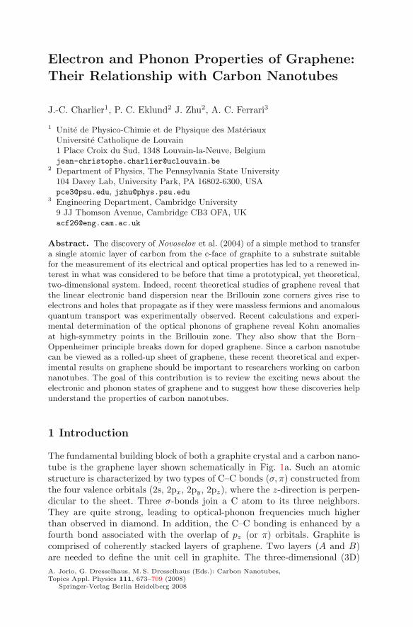
Fig. 19. Comparison between the computed frequency of the LO and the TO pho-non in SWNTs (lines) and the experimental position of the G+ and the G− Ramanpeak in metallic and semiconducting tubes as measured by various authors [19]. Cal-culations include the dynamic effects and a correction for the curvature effects [19]
same tight–binding model as was used for graphene, it is possible to showthat the EPC affects the LO mode only and acts in two different ways. First,it is responsible for the onset of a Kohn anomaly resulting in a strong down-shift of the LO frequency. Secondly, in agreement with the Fermi golden rule,it reduces the LO–phonon lifetime, resulting in an increase of the phononlinewidth. Consistent with this view, the G− peak in metallic tubes does notoriginate from a curvature-downshifted TO phonon, as in semiconductingtubes, but is derived from an EPC-affected LO mode [19, 20]. The predictiongiven by the dynamic, time-dependent model can be compared with the datafrom Raman spectroscopy. Figure 19 shows that the calculated frequencies ofthe TO and LO modes in metallic SWNTs are in reasonable agreement withthe position of the G+ and G− Raman peaks. This suggests that the G+
and G− peaks of metallic nanotubes should be assigned to TO (tangential)and LO (axial) modes, the opposite of semiconducting nanotubes [19, 20].
In SWNTs, due to the reduced dimensionality, the nonadiabatic contribu-tions are essential to describe the phonons [19] and they should be more im-portant in the case of doped SWNTs [22]. Thus, the shape of the G peak willbe affected by doping in a similar fashion to doped graphene. Furthermore,due to energy conservation, measuring a metallic nanotube off resonance canresult in a sharp G− feature. We can thus simply understand the reasonfor the large variety of G− lineshapes reported in the literature. Finally, thenonadiabatic Kohn anomaly at Γ also explains the observed electronic tem-perature dependence of the Raman spectra [19].
It is important to note the following on the shape of the G− peak [20].The peak shape observed in an actual experiment depends on the couplingbetween the experimental probe and the system, as discussed in the seminalpaper by Fano [126]. Indeed, if the laser couples not only to the G− phonon,

Electron and Phonon Properties of Graphene 701
but also to the continuum that broadens the phonon, the Raman spectrumshows an asymmetric Fano profile [126]. Thus, the detection of an asym-metric Fano profile in a Raman measurement gives information on how theelectromagnetic radiation couples to the system, but not on the origin of thebroadening. Here, we discussed how the broadening of the G− peak in metal-lic nanotubes can be mainly attributed to the coupling of the LO phononto the continuum of the electron–hole excitations, not to phonon–plasmoncoupling. This does not imply that a Fano-like profile cannot be observed inexperiments.
5 Outlook
In the past two years, tens of papers have been published and more than 600papers have been posted on graphene. Thus, by no means could we give acomprehensive review of this fast-moving field in the limited space availablehere. So, we have focused on the basic electronic and phonon properties ofgraphene and their relation to nanotubes.
Even if graphene research is at the beginning, scientists can now exploitthe large amount of expertise acquired in the study of carbon nanotubes.Almost all the experiments reported on nanotubes are now being performedon graphene. These range from transistor fabrication, to nanoelectromechan-ical assemblies, to spin transport to optoelectronics. Furthermore, bilayer andfew-layer graphene samples could lead to a variety of interesting new physicsand applications. A research area that is still largely unexplored is the growthof graphene layers on a substrate of choice. Large-scale deposition of grapheneis the needed breakthrough to make this new material viable for electronicapplications. Once this is achieved, standard top-down processes could beutilized for large-area production of devices. This is a major advantage com-pared to nanotubes, for which on-demand chirality is still a dream.
Acknowledgements
J. C. Charlier acknowledges the National Fund for Scientific Research [FNRS]of Belgium for financial support. A. C. Ferrari acknowledges support from TheRoyal Society and The Leverhulme Trust. P. C. Eklund and J. Zhu acknowl-edge support from the National Science Foundation NIRT program, and wethank A. Gupta and T. J. Russin for helpful discussions and assistance withpreparing figures.
References
[1] P. R. Wallace: The band theory of graphite, Phys. Rev. 71, 622 (1947) 674[2] L. M. Viculis, J. J. Mack, R. B. Kaner: A chemical route to carbon nanoscrolls,
Science 299, 1361 (2003) 674

702 J.-C. Charlier et al.
[3] L. M. Viculis, J. J. Mack, O. M. Mayer, H. T. Hahn, R. B. Kaner: Intercalationand exfoliation routes to graphite nanoplatelets, J. Mater. Chem. 15, 974(2005) 674
[4] S. Niyogi, E. Bekyarova, M. E. Itkis, J. L. McWilliams, M. A. Hammon,R. C. Haddon: Solution properties of graphite and graphene, J. Am. Chem.Soc. 128, 7720 (2006) 674
[5] S. Stankovich, D. A. Dikin, G. H. B. Dommett, K. M. Kohlhass, E. J. Zimmey,E. A. Stach, R. D. Piner, S.-B. T. Nguyen, R. S. Ruoff: Graphene-basedcomposite materials, Nature 442, 282 (2006) 674
[6] S. Stankovich, R. D. Piner, X. Chen, N. Wu, T. Nguyen, R. S. Ruoff: Stableaqueous dispersions of graphitic nanoplatelets via the reduction of exfoliatedgraphite oxide in the presence of poly(sodium 4-styrenesulfonate), J. Mater.Chem. 16, 155 (2006) 674
[7] K. S. Novoselov, A. K. Geim, S. V. Morozov, D. Jiang, S. V. Dubonos,I. V. Girgorieva, A. A. Firsov: Electric field effect in atomically thin carbonfilms, Science 306, 666 (2004) 674, 686
[8] Y. B. Zhang, J. P. Small, W. V. Pontius, P. Kim: Fabrication and electric-field-dependent transport measurements of mesoscopic graphite devices,Appl. Phys. Lett. 86, 073104 (2005) 674
[9] I. Forbeaux, J. M. Themlin, J. M. Debever: High-temperature graphitizationof the 6H-SiC (000(1)over-bar) face, Surf. Sci. 442, 9 (1999) 674
[10] C. Berger, Z. M. Song, T. B. Li, X. B. Li, A. Y. Ogbazghi, R. Feng, Z. T. Dai,A. N. Marchenkov, E. H. Conrad, P. N. First, W. A. de Heer: Ultrathinepitaxial graphite: 2D electron gas properties and a route toward graphene-based nanoelectronics, J. Phys. Chem. B 108, 19912 (2004) 674
[11] T. Ohta, A. Bostwick, T. Seyller, K. Horn, E. Rotenberg: Controlling theelectronic structure of bilayer graphene, Science 313, 951 (2006) 674, 684,685
[12] E. Rolling, G. H. Gweon, S. Y. Zhou, B. S. Mun, J. L. McChesney, B. S. Hus-sain, A. Fedorov, P. N. First, W. A. de Heer, A. Lanzara: Synthesis and char-acterization of atomically thin graphite films on a silicon carbide substrate,J. Phys. Chem. Solids 67, 2172 (2006) 674
[13] K. S. Novoselov, A. K. Geim, S. V. Morozov, D. Jiang, M. I. Katsnelson,I. V. Girgorieva, S. V. Dubonos, A. A. Firsov: Two-dimensional gas of mass-less Dirac fermions in graphene, Nature 438, 197 (2005) 674, 676, 679, 680,681
[14] Y. Zhang, Y. W. Tan, H. L. Stormer, P. Kim: Experimental observation of thequantum Hall effect and Berry’s phase in graphene, Nature 438, 201 (2005)674, 676, 678, 679, 680, 681
[15] A. K. Geim, K. S. Novoselov: The rise of graphene, Nature Mater. 6, 183(2007) 674, 678, 679
[16] M. Born, R. Oppenheimer: Ann. Phys. 84, 457 (1927) 675, 695[17] S. Pisana, M. Lazzeri, C. Casiraghi, K. Novoselov, A. K. Geim, A. C. Ferrari,
F. Mauri: Breakdown of the adiabatic Born–Oppenheimer approximation ingraphene, Nature Mater. 6, 198 (2007) 675, 690, 691, 694, 695, 696, 698
[18] S. Piscanec, M. Lazzeri, F. Mauri, A. Ferrari, J. Robertson: Kohn anomaliesand electron–phonon interactions in graphite, Phys. Rev. Lett. 93, 185503(2004) 675, 688, 689, 691, 693, 694, 695

Electron and Phonon Properties of Graphene 703
[19] S. Piscanec, M. Lazzeri, J. Robertson, A. C. Ferrari, F. Mauri: Opticalphonons in carbon nanotubes: Kohn anomalies, Peierls distortions, and dy-namic effects, Phys. Rev. B 75, 035427 (2007) 675, 688, 689, 690, 697, 698,699, 700
[20] M. Lazzeri, S. Piscanec, F. Mauri, A. C. Ferrari, J. Robertson: Phononlinewidths and electron–phonon coupling in graphite and nanotubes, Phys.Rev. B 73, 155426 (2006) 675, 688, 689, 690, 697, 698, 699, 700
[21] M. Lazzeri, S. Piscanec, F. Mauri, A. C. Ferrari, J. Robertson: Electron trans-port and hot phonons in carbon nanotubes, Phys. Rev. Lett. 95, 236802(2005) 675, 688, 689
[22] N. Caudal, A. M. Saitta, M. Lazzeri, F. Mauri: Kohn anomalies and nonadi-abaticity in doped carbon nanotubes, Phys. Rev. B 75, 115423 (2007) 675,700
[23] J.-C. Charlier, X. Blase, S. Roche: Electronic and transport properties ofnanotubes, Rev. Mod. Phys. 79, 677–732 (2007) 675, 676, 677
[24] J. C. Slonczewski, P. R. Weiss: Band structure of graphite, Phys. Rev. 109,272 (1958) 678
[25] K. S. Novoselov, D. Jiang, F. Schedin, T. J. Booth, V. V. Khotkevich,S. V. Morozov, A. K. Geim: Two-dimensional atomic crystals, Proc. NatureAcad. Sci. USA 102, 10451 (2005) 678
[26] C. Berger, Z. Song, X. Li, X. Wu, N. Brown, C. Naud, D. Mayou, T. Li,J. Hass, A. N. Marchenkov, E. H. Conrad, P. N. First, W. A. De Heer: Elec-tronic confinement and coherence in patterned epitaxial graphene, Science312, 1191 (2006) 679
[27] K. Nomura, A. H. MacDonald: Quantum transport of massless Diracfermions, Phys. Rev. Lett. 98, 076602 (2007) 679
[28] K. S. Novoselov, E. McCann, S. V. Morozov, V. I. F. M. I. Katsnelson,U. Zeitler, D. Jiang, F. Schedin, A. K. Geim: Unconventional quantum Halleffect and Berry’s phase of 2 pi in bilayer graphene, Nature Phys. 2, 177(2006) 679, 685
[29] S. V. Morozov, K. S. Novoselov, M. I. Katsnelson, F. Schedin, L. A. Pono-marenko, D. Jiang, A. K. Geim: Strong suppression of weak localization ingraphene, Phys. Rev. Lett. 97, 016801 (2006) 679
[30] V. M. Galitski, S. Adam, S. D. Sarma: Statistics of random voltage fluc-tuations and the low-density residual conductivity of graphene, arXiv Url:cond-mat/0702117 679
[31] F. D. M. Haldane: Model for a quantum Hall effect without Landau levels:Condensed-matter realization of the ”parity anomaly“, Phys. Rev. Lett. 61,2015 (1988) 679
[32] Y. S. Zheng, T. Ando: Hall conductivity of a two-dimensional graphite system,Phys. Rev. B 65, 245420 (2002) 679
[33] M. L. Sadowski, G. Martinez, M. Potemski, C. Berger, W. A. de Heer: Landaulevel spectroscopy of ultrathin graphite layers, Phys. Rev. Lett. 97, 266405(2006) 679
[34] Z. Jiang, E. A. Henriksen, L. C. Tung, Y.-J. Wang, M. E. Schwartz,M. Y. Han, P. Kim, H. L. Stormer: Infrared spectroscopy of Landau levels ofgraphene, Phys. Rev. Lett. 98, 197403 (2007) 679, 680

704 J.-C. Charlier et al.
[35] R. S. Deacon, K.-C. Chuang, R. J. Nicholas, K. S. Novoselov, A. K. Geim:Cyclotron resonance study of the electron and hole velocity in graphene mono-layers, Phys. Rev. B 76 (8), 081406 (2007) 679, 680
[36] K. S. Novoselov, Z. Jiang, Y. Zhang, S. V. Morozov, H. L. Stormer, U. Zeitler,J. C. Maan, G. S. Boebinger, P. Kim, A. K. Geim: Room-temperature quan-tum Hall effect in graphene, Science 315, 1379 (2007) 679
[37] M. Berry: Quantal phase-factors accompanying adiabatic changes, Proc. R.Soc. Lond. A 392, 45 (1984) 680
[38] D. Shoenberg: Magnetic Oscillations in Metals (Cambridge University Press,Cambridge 1984) 680
[39] Y. Zhang, Z. Jiang, J. P. Small, M. S. Purewal, Y. W. Tan, M. Fazlollahi,J. D. Chudow, J. A. Jaszczak, H. L. Stormer, P. Kim: Landau-level splittingin graphene in high magnetic fields, Phys. Rev. Lett. 96, 136806 (2006) 681,696
[40] D. A. Abanin, K. S. Novoselov, U. Zeitler, P. A. Lee, A. K. Geim, L. S. Levi-tov: Dissipative quantum Hall effect in graphene near the Dirac point, Phys.Rev. Lett. 98, 196806 (2007) 681
[41] K. Yang: Spontaneous symmetry breaking and quantum Hall effect ingraphene, Solid State Comm. 143, 27 (2007) 681
[42] K. Nakada, M. Fujita, G. Dresselhaus, M. S. Dresselhaus: Edge state ingraphene ribbons: Nanometer size effect and edge shape dependence, Phys.Rev. B 54, 17954 (1996) 681, 682
[43] K. Wakabayashi, M. Fujita, H. Ajiki, M. Sigrist: Electronic and magneticproperties of nanographite ribbons, Phys. Rev. B 59, 8271 (1999) 681, 682,683
[44] Y. Miyamoto, K. Nakada, M. Fujita: First-principles study of edge states ofH-terminated graphitic ribbons, Phys. Rev. B 59, 9858 (1999) 681, 682
[45] T. Kawai, Y. Miyamoto, O. Sugino, Y. Koga: Graphitic ribbons withouthydrogen-termination: Electronic structures and stabilities, Phys. Rev. B 62,R16349 (2000) 681, 682
[46] S. Okada, A. Oshiyama: Magnetic ordering in hexagonally bonded sheets withfirst-row elements, Phys. Rev. Lett. 87, 146803 (2001) 681, 682, 683
[47] H. Lee, Y.-W. Sun, N. Park, S. Han, J. Yu: Magnetic ordering at the edgesof graphitic fragments: Magnetic tail interactions between the edge-localizedstates, Phys. Rev. B 72, 174431 (2005) 681, 682, 683
[48] M. Ezawa: Peculiar width dependence of the electronic properties of carbonnanoribbons, Phys. Rev. B 73, 045432 (2006) 681, 682
[49] L. Brey, H. A. Fertig: Electronic states of graphene nanoribbons studied withthe Dirac equation, Phys. Rev. B 73, 235411 (2006) 681, 682
[50] K.-I. Sasaki, S. Murakami, R. Saito: J. Phys. Soc. Jpn. 75, 074713 (2006)681, 682
[51] D. A. Abanin, P. A. Lee, L. S. Levitov: Spin-filtered edge states and quantumHall effect in graphene, Phys. Rev. Lett. 96, 176803 (2006) 681, 682
[52] Y.-W. Son, M. L. Cohen, S. G. Louie: Energy gaps in graphene nanoribbons,Phys. Rev. Lett. 97, 216803 (2006) 681, 682, 683
[53] Y.-W. Son, M. L. Cohen, S. G. Louie: Erratum: Energy gaps in graphenenanoribbons, Phys. Rev. Lett. 98, 089901 (2007) 681, 682, 683
[54] Y.-W. Son, M. L. Cohen, S. G. Louie: Half-metallic graphene nanoribbons,Nature 444, 347 (2006) 681, 682, 683

Electron and Phonon Properties of Graphene 705
[55] Y. Kobayashi, K. Fukui, T. Enoki, K. Kusakabe, Y. Kaburagi: Observationof zigzag and armchair edges of graphite using scanning tunneling microscopyand spectroscopy, Phys. Rev. B 71, 193406 (2005) 682
[56] C. L. Kane, E. J. Mele: Z(2) topological order and the quantum spin Halleffect, Phys. Rev. Lett. 95, 146802 (2005) 683
[57] D. Prezzi, D. Varasano, A. Ruini, E. Molinari: Optical properties of graphenenanoribbons: The role of many-body effects, arXiv:0706.0916 (2007) 683
[58] M. Y. Han, B. Ozyilmaz, Y. Zhang, P. Kim: Energy band-gap engineering ofgraphene nanoribbons, Phys. Rev. Lett. 98, 206805 (2007) 683
[59] Z. Chen, Y.-M. Lin, M. J. Rooks, P. Avouris: Graphene nano-ribbon elec-tronics, arXiv URL: cond-mat/0701599 683
[60] F. Cervantes-Sodi, G. Csanyi, S. Piscanec, A. C. Ferrari: Edge functionalisedand substitutional doped graphene nanoribbons: electronic and spin proper-ties, Cond Mat 0711.2340 (2007) 683
[61] G. Dresselhaus, M. S. Dresselhaus: Spin-orbit interaction in graphite, Phys.Rev. 140, 401 (1965) 683
[62] J.-C. Charlier, X. Gonze, J.-P. Michenaud: First-principles study of the elec-tronic properties of graphite, Phys. Rev. B 43, 4579 (1991) 684
[63] J.-C. Charlier, X. Gonze, J.-P. Michenaud: First-principles study of the elec-tronic properties of simple hexagonal graphite, Phys. Rev. B 46, 4531 (1992)684
[64] J.-C. Charlier, X. Gonze, J.-P. Michenaud: First-principles study of the stack-ing effect on the electronic properties of graphite(s), Carbon 32, 289–299(1994) 684
[65] J.-C. Charlier, X. Gonze, J.-P. Michenaud: Graphite interplanar bonding:electronic delocalization and van der Waals interaction, Europhys. Lett. 28,403–408 (1994) 684
[66] S. Latil, L. Henrard: Charge carriers in few-layer graphene films, Phys. Rev.Lett. 97, 036803 (2006) 684
[67] F. Guinea, A. H. Castro-Neto, N. M. R. Peres: Electronic states and Landaulevels in graphene stacks, Phys. Rev. B 73, 245426 (2006) 684
[68] J.-C. Charlier, J.-P. Michenaud, P. Lambin: Tight-binding density of elec-tronic states of pregraphitic carbon, Phys. Rev. B 46, 4540 (1992) 684
[69] E. McCann, V. I. Fal’ko: Landau-level degeneracy and quantum Hall effectin a graphite bilayer, Phys. Rev. Lett. 96, 086805 (2006) 684, 685
[70] E. V. Castro, K. S. Novoselov, S. V. Morozov, N. M. R. Peres, J. M. B. L. dosSantos, J. Nilsson, F. Guinea, A. K. Geim, A. H. Castro-Neto: Biased bilayergraphene: Semiconductor with a gap tunable by electric field effect, arXivURL: cond-mat/0611342 685
[71] C. Casiraghi, A. Hartschuh, E. Lidorikis, H. Qian, H. Harutyunyan, T. Gokus,K. S. Novoselov, A. C. Ferrari: Rayleigh imaging of graphene and graphenelayers, Nano Lett. 7, 2711 (2007) 686
[72] A. C. Ferrari, J. C. Meyer, V. Scardaci, C. Casiraghi, M. Lazzeri, F. Mauri,S. Piscanec, D. Jiang, K. S. Novoselov, S. Roth, A. K. Geim: Raman spectrumof graphene and graphene layers, Phys. Rev. 97, 187401 (2006) 686, 690,691, 692, 693, 694, 696
[73] A. C. Ferrari, J. Robertson: Raman spectroscopy in carbons: From nanotubesto diamond, Philos. Trans. Roy. Soc. A 362, 2267–2565 (2004) 687

706 J.-C. Charlier et al.
[74] C. Castiglioni, F. Negri, M. Rigolio, G. Zerbi: Raman activation in disordered
graphites of the A′1 symmetry forbidden k �= 0 phonon: The origin of the D
line, J. Chem. Phys. 115, 3769 (2001) 687[75] C. Castiglioni, M. Tommasini, G. Zerbi: Raman spectroscopy of polyconju-
gated molecules and materials: Confinement effect in one and two dimensions,Philos. Trans. R. Soc. Lond. A 362, 2425 (2004) 687
[76] F. Tuinstra, J. Koenig.: Raman spectrum of graphite, J. Chem. Phys. 53,1126 (1970) 687, 688, 693
[77] A. C. Ferrari, J. Robertson: Interpretation of Raman spectra of disorderedand amorphous carbon, Phys. Rev. B 61, 14095 (2000) 687, 688, 693
[78] R. J. Nemanich, S. A. Solin: First- and second-order Raman scattering fromfinite-size crystals of graphite, Phys. Rev. B 20, 392 (1979) 687, 690
[79] R. Al-Jishi, G. Dresselhaus: Lattice-dynamical model for graphite, Phys. Rev.B, 26, 4514 (1982) 687
[80] R. P. Vidano, D. B. Fishbach, L. J. Willis, T. M. Loehr: Observation ofRaman band shifting with excitation wavelength for carbons and graphites,Solid State Commun. 39, 341 (1981) 687, 690
[81] I. Pocsik, M. Hundhausen, M. Koos, L. Ley: DC electrical properties of amor-phous carbon with different bonding hybridization, J. Non-Cryst. Solids 227–230, 1087 (1998) 687, 688
[82] P. Lespade, A. Marchard, M. Couzi, F. Cruege: Caracterisation de materiauxcarbones par microspectrometrie Raman, Carbon 22, 375 (1984) 687
[83] C. Thomsen, S. Reich: Double resonant Raman scattering in graphite, Phys.Rev. Lett. 85, 5214 (2000) 687, 688, 691
[84] A. V. Baranov, A. N. Bekhterev, Y. S. Bobovich, V. I. Petrov: Interpretationof some peculiarities in Raman spectra of graphite and glassy carbon, Opt.Spektrosk. 62, 1036 (1987) 687
[85] J. Maultzsch, S. Reich, C. Thomsen, H. Requardt: Phonon dispersion ingraphite, P. Ordejon. Phys. Rev. Lett. 92, 075501 (2004) 688
[86] M. J. Matthews, M. A. Pimenta, G. Dresselhaus, M. S. Dresselhaus, M. Endo:Origin of dispersive effects of the Raman D band in carbon materials, Phys.Rev. B 59, 6585 (1999) 687, 688
[87] A. Gruneis, R. Saito, T. Kimura, L. G. Cancado, M. A. Pimenta, A. Jorio,A. G. S. Filho, G. Dresselhaus, M. S. Dresselhaus: Determination of two-dimensional phonon dispersion relation of graphite by Raman spectroscopy,Phys. Rev. B 65, 155405 (2002) 687, 688
[88] R. Saito, A. Jorio, A. G. S. Filho, G. Dresselhaus, M. S. Dresselhaus, M. A. Pi-menta: Probing phonon dispersion relations of graphite by double resonanceRaman scattering, Phys. Rev. Lett. 88, 027401 (2002) 687, 688
[89] A. C. Ferrari, J. Robertson.: Resonant Raman spectroscopy of disordered,amorphous, and diamondlike carbon, Phys. Rev. B, 64, 075414 (2001) 687,688, 691
[90] C. Mapelli, C. Castiglioni, G. Zerbi, K. Mullen: Common force field forgraphite and polycyclic aromatic hydrocarbons, Phys. Rev. B 60, 12710(1999) 688
[91] G. Kresse, J. Furthmuller, J. Hafner: Ab initio force constant approach tophonon dispersion relations of diamond and graphite, Europhys. Lett. 32,729 (1995) 688

Electron and Phonon Properties of Graphene 707
[92] P. Pavone, R. Bauer, K. Karch, O. Schutt, S. Vent, W. Windl, D. Strauch,S. Baroni, S. de Gironcoli: Ab initio phonon calculations in solids, Physica B,219–220, 439 (1996) 688
[93] L. Wirtz, A. Rubio: The phonon dispersion of graphite revisited, Solid. StateCommun. 131, 141 (2004) 688
[94] O. Dubay, G. Kresse: Accurate density functional calculations for the phonondispersion relations of graphite layer and carbon nanotubes, Phys. Rev. B 67,035401 (2003) 688
[95] W. Kohn: Image of the Fermi surface in the vibration spectrum of a metal,Phys. Rev. Lett. 2, 393 (1959) 688
[96] A. Javey, J. Guo, M. Paulsson, Q. Wang, D. Mann, M. Lundstrom, H. Dai:High-field quasiballistic transport in short carbon nanotubes, Phys. Rev. Lett.92, 106804 (2004) 689
[97] J. Y. Park, S. Rosenblatt, Y. Yaish, V. Sazonova, H. Ustunel, S. Braig,T. A. Arias, P. W. Brouwer, P. L. McEuen: Electron–phonon scattering inmetallic single-walled carbon nanotubes, Nano Lett. 4, 517 (2004) 689
[98] V. Perebeinos, J. Tersoff, P. Avouris: Electron–phonon interaction and trans-port in semiconducting carbon nanotubes, Phys. Rev. Lett. 94, 086802 (2005)689
[99] Z. Yao, C. L. Kane, C. Dekker: High-field electrical transport in single-wallcarbon nanotubes, Phys. Rev. Lett. 84, 2941 (2000) 689
[100] J. Jiang, R. Saito, A. Gruneis, G. Dresselhaus, M. S. Dresselhaus: Electron–phonon interaction and relaxation time in graphite, Chem. Phys. Lett. 392,383 (2004) 689
[101] J. Jiang, R. Saito, A. Gruneis, S. G. Chou, G. G. Samsonidze, A. Jorio,G. Dresselhaus, M. S. Dresselhaus: Photoexcited electron relaxation processesin single-wall carbon nanotubes, Phys. Rev. B 71, 045417 (2005) 689
[102] G. Pennington, N. Goldsman: Semiclassical transport and phonon scatteringof electrons in semiconducting carbon nanotubes, Phys. Rev. B 68, 045426(2004) 689
[103] G. D. Mahan: Electron–optical phonon interaction in carbon nanotubes,Phys. Rev. B 68, 125409 (2003) 689
[104] P. H. Tan, C. Y. Hu, J. Dong, W. C. Shen, B. F. Zhang: Polarization prop-erties, high-order Raman spectra, and frequency asymmetry between Stokesand anti-Stokes scattering of Raman modes in a graphite whisker, Phys. RevB 64, 214301 (2000) 690
[105] V. Scardaci, P. H. Tan, A. C. Ferrari, et al.: unpublished 690[106] M. Lazzeri, F. Mauri: Nonadiabatic Kohn anomaly in a doped graphene
monolayer, Phys. Rev. Lett. 97, 266407 (2006) 690, 695, 696, 698[107] A. Gupta, P. C. Eklund: unpublished 691[108] Y. Wang, D. C. Aolsmeyer, R. L. McCreery: Raman spectroscopy of carbon
materials: Structural basis of observed spectra, Chem. Mater. 2, 557 (1990)691
[109] A. Gupta, P. C. Eklund: unpublished 691[110] P. H. Tan, C. Casiraghi, A. C. Ferrari: unpublished 693[111] J. Yan, Y. Zhang, P. Kim, A. Pinczuk: Electric field effect tuning of electron–
phonon coupling in graphene, Phys. Rev. Lett. 98, 166802 (2007) 694, 695[112] T. Ando: Anomaly of optical phonon in monolayer graphene, J. Phys. Soc.
Jpn. 75, 124701 (2006) 695

708 J.-C. Charlier et al.
[113] A. H. Castro-Neto, F. Guinea.: Electron–phonon coupling and Raman spec-troscopy in graphene, Phys. Rev. B 75, 045404 (2007) 695
[114] G. Moos, C. Gahl, R. Fasel, M. Wolf, T. Hertel: Anisotropy of quasiparticlelifetimes and the role of disorder in graphite from ultrafast time-resolvedphotoemission spectroscopy, Phys. Rev. Lett. 87, 267402 (2001) 696
[115] T. Kampfrath, L. Perfetti, F. Schapper, C. Frischkorn, M. Wolf: Stronglycoupled optical phonons in the ultrafast dynamics of the electronic energyand current relaxation in graphite, Phys. Rev. Lett. 95, 187403 (2005) 696
[116] A. Gupta, G. Chen, P. Joshi, S. Tadigadapa, P. C. Eklund: Raman scatteringfrom high-frequency phonons in supported n-graphene layer films, Nano Lett.6, 2667 (2006) 696
[117] D. Graf, F. Molitor, K. Ensslin, C. Stampfer, A. Jungen, C. Hierold, L. Wirtz:Spatially resolved Raman spectroscopy of single- and few-layer graphene,Nano Lett. 7, 238 (2007) 696
[118] C. Casiraghi, S. Pisana, K. S. Novoselov, A. K. Geim, A. C. Ferrari: Ramanfingerprint of charged impurities in graphene, Cond-Mat 0709.2566 (2007)697
[119] C. Casiraghi, S. Pisana, K. S. Novoselov, A. K. Geim, A. C. Ferrari: Ramanfingerprint of charged impurities in graphene, Appl. Phys. Lett. in press. 697
[120] A. Das, S. Pisana, S. Piscanec, B. Chakraborty, S. K. Saha, U. V. Waghmare,R. Yiang, H. R. Krishnamurhthy, A. K. Geim, A. C. Ferrari, A. K. Sood:Electrochemically gated graphene: Monitoring dopants by Raman scattering,cond mat 0709.1174 (2007) 697
[121] V. Zolyomi, J. Kurti: First-principles calculations for the electronic bandstructures of small diameter single-wall carbon nanotubes, Phys. Rev. B, 70,085403 (2004) 697
[122] D. Connetable, D., G.-M. Rignanese, J.-C. Charlier, X. Blase: Room temper-ature Peierls distortion in small diameter nanotubes, Phys. Rev. Lett. 94,015503 (2005) 697
[123] A. Jorio, R. Saito, M. S. Dresselhaus, G. Dressselhaus: One contribution of13 to a theme ’Raman spectroscopy in carbons: from nanotubes to diamond’,Trans. Roy. Soc. A 362, 2311 (2004) 699
[124] S. D. M. Brown, A. Jorio, P. Corio, M. S. Dresselhaus, G. Dresselhaus,R. Saito, K. Kneipp: Origin of the Breit–Wigner–Fano lineshape of the tan-gential g-band feature of metallic carbon nanotubes, Phys. Rev. B 63, 155414(2001) 699
[125] K. Kempa: Gapless plasmons in carbon nanotubes and their interactions withphonons, Phys. Rev. B 66, 195406 (2002) 699
[126] U. Fano: Effects of configuration interaction on intensities and phase shifts,Phys. Rev. 124, 1866 (1961) 700, 701
Index
graphene, 676
π orbital, 673
σ-bond, 673
2D peak, 690
band structure, 685
Berry’s phase, 676

Electron and Phonon Properties of Graphene 709
bilayer, 685, 693Born–Oppenheimer approximation,
675, 695C–C bond, 673carrier density, 678D band, 687Dirac fermion, 674Dirac point, 674doping, 694double resonance, 687electron–phonon interaction in
graphene, 675electronic group velocity, 676epitaxial graphitic film, 674G band, 687, 696G′ band, 690graphene FET, 678half integer quantum Hall effect,
679–681Hall resistance, 680integer quantum Hall effect, 674Kohn anomaly, 675, 686, 697, 698Landau level, 679magnetoresistance, 680massless Dirac fermion, 674
minimum quantum conductivity, 679
mobility, 678
non-Born–Oppenheimer effect, 675
phonon dispersion, 687, 688
Raman linewidth, 689
Raman spectroscopy, 686, 690
resistivity, 678
Shubnikov–de Haas oscillation, 676
single-particle Zeeman splitting, 681
tight-binding Hamiltonian, 676
turbostratic random stacking, 684
nanoribbon, 681
armchair edge, 683
chemically functionalized, 683
many-body correction, 683
self-energy, 683
spin-polarization effect, 683
spintronic, 683
zigzag edge, 683
nanotube, 698
G band, 698
LO mode, 698
TO mode, 698