elec 5200/6200 computer architecture and design spring 2017 · elec 5200/6200 computer architecture...
TRANSCRIPT

ELEC 5200/6200
Computer Architecture and Design
Spring 2017 Lecture 4: Datapath and Control
2/6/2017 ELEC 5200-001/6200-001 Lecture 4 1
Ujjwal Guin, Assistant Professor
Department of Electrical and Computer Engineering
Auburn University, Auburn, AL 36849
http://www.auburn.edu/~uzg0005/
Adapted from Dr. Chen-Huan Chiang (Intel) and Prof. Vishwani D. Agrawal (Auburn University)
[Adapted from Computer Organization and Design, Patterson & Hennessy, 2014]
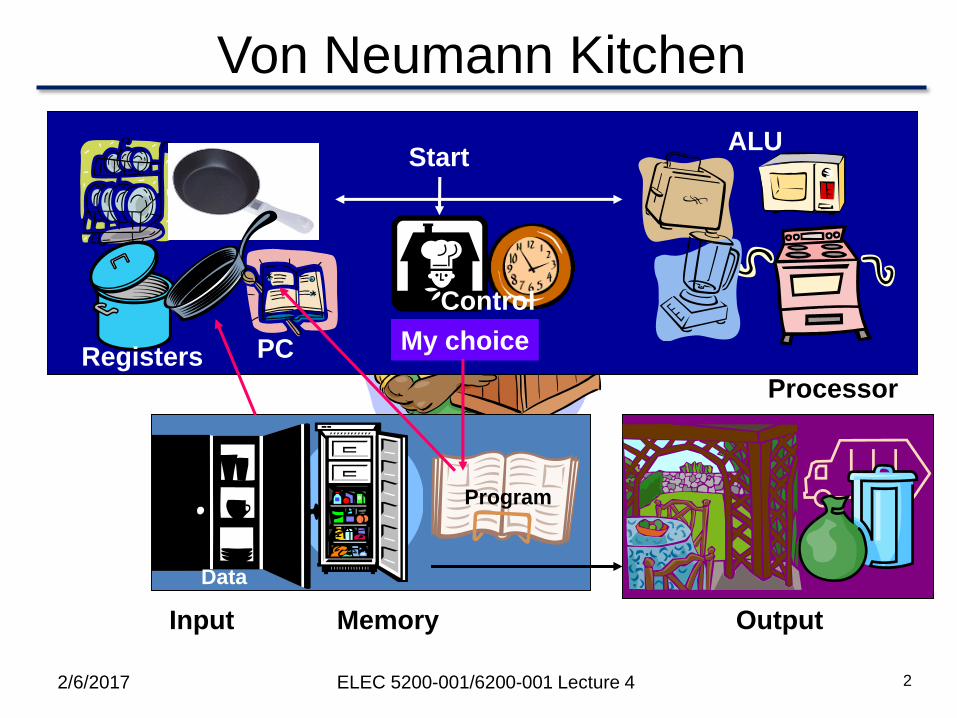
Von Neumann Kitchen
2/6/2017 ELEC 5200-001/6200-001 Lecture 4 2
Registers
ALU
Control
Memory Output
Program
Data
My choicePC
Start
Processor
Input

Where Does It All Begin?
In a register called program counter (PC).
PC contains the memory address of the next
instruction to be executed.
In the beginning, PC contains the address of the
memory location where the program begins.
2/6/2017 ELEC 5200-001/6200-001 Lecture 4 3

Where is the Program?
2/6/2017 ELEC 5200-001/6200-001 Lecture 4 4
Machine code
of program
Memory
Start
address
Program counter
(register)
Processor

How Does It Run?
2/6/2017 ELEC 5200-001/6200-001 Lecture 4 5
Start
PC has memory address where program begins
Fetch instruction word from memory address in PC
and increment PC ← PC + 4 to point to next instruction
Decode instruction
Program
complete?
YesNo
STOP
Execute instruction
Save result in register or memory

Datapath and Control
Datapath
– Memory, registers, adders, ALU, and communication buses.
– Each step (fetch, decode, execute, save result) requires
communication (data transfer) paths between memory, registers and
ALU.
Control
– Datapath for each step is set up by control signals that set up
dataflow directions on communication buses and select ALU and
memory functions.
– Control signals are generated by a control unit consisting of one or
more finite-state machines.
2/6/2017 ELEC 5200-001/6200-001 Lecture 4 6
Single-Cycle Processor
Simplified MIPS - Datapath

Abstract View of MIPS
2/6/2017 ELEC 5200-001/6200-001 Lecture 4 8A
LU
Data
Register #
Register #
Register #
Regis
ters
Instruction
Instructionmemory
Address
Data
Address
Data Memory
PC
4
Add
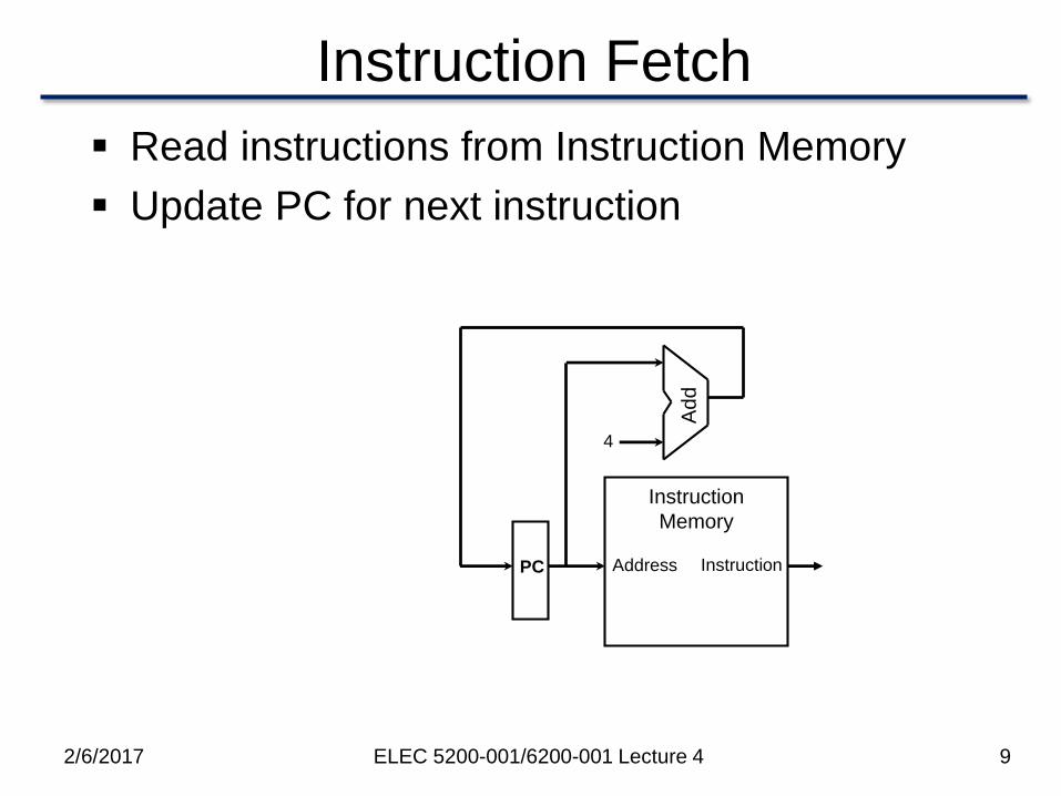
Instruction Fetch
9
Address Instruction
Instruction
Memory
Add
PC
4
Read instructions from Instruction Memory
Update PC for next instruction
2/6/2017 ELEC 5200-001/6200-001 Lecture 4
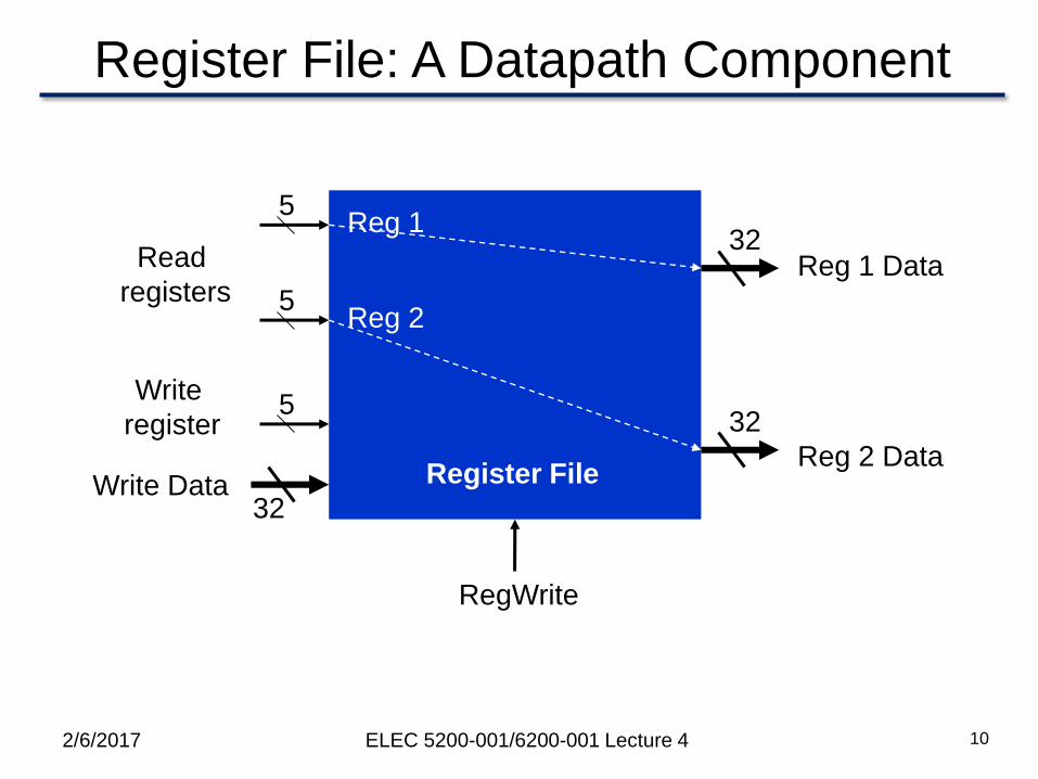
Register File: A Datapath Component
2/6/2017 ELEC 5200-001/6200-001 Lecture 4 10
Write
register
Reg 1 Data
Reg 2 Data
5
5
5
32
32
32
Reg 1
Reg 2
Read
registers
Write Data
RegWrite
Register File
11
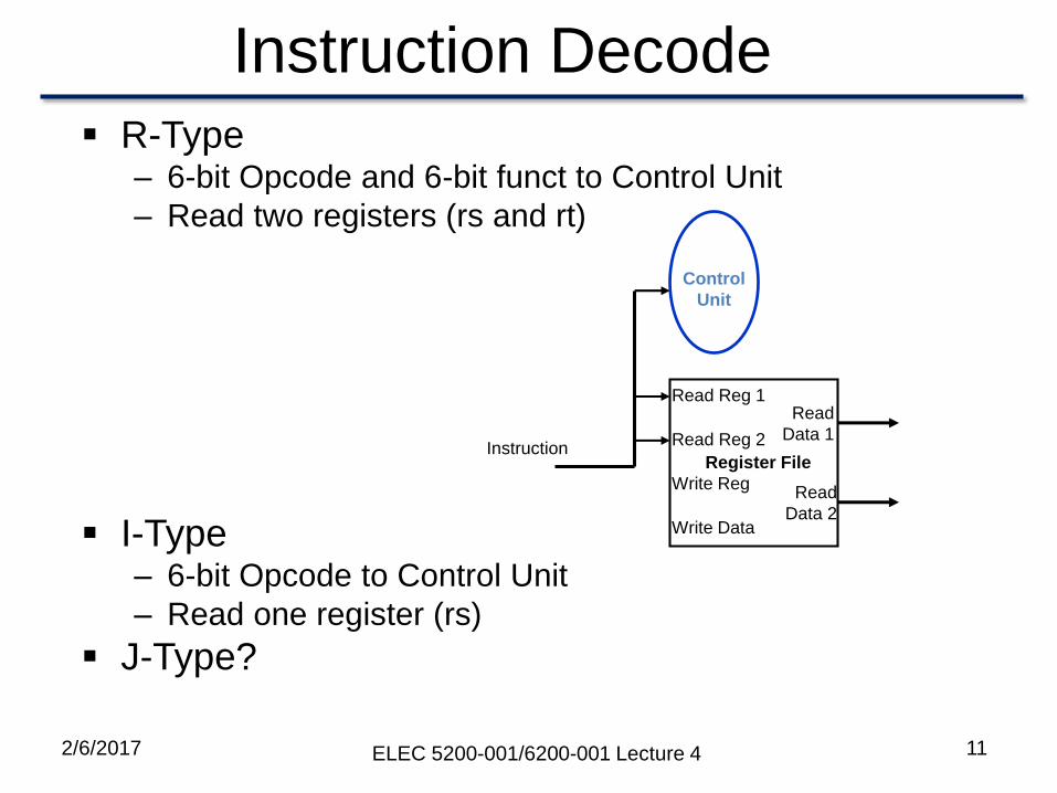
Instruction Decode R-Type
– 6-bit Opcode and 6-bit funct to Control Unit
– Read two registers (rs and rt)
I-Type– 6-bit Opcode to Control Unit
– Read one register (rs)
J-Type?
Instruction
Write Data
Read Reg 1
Read Reg 2
Write Reg
Register File
Read
Data 1
Read
Data 2
Control
Unit
2/6/2017 ELEC 5200-001/6200-001 Lecture 4

Execute: R-Type
Why RegWrite?
12
Instruction
Write Data
Read Reg 1
Read Reg 2
Write Reg
Read
Data 1
Read
Data 2
ALU
zero
ALU OperationRegWrite
opcode rs rt rd shamt funct
31 - 26 | 25-21 | 20 - 16 | 15 - 11 | 10 – 6 | 5 – 0 |
Register File
2/6/2017 ELEC 5200-001/6200-001 Lecture 4
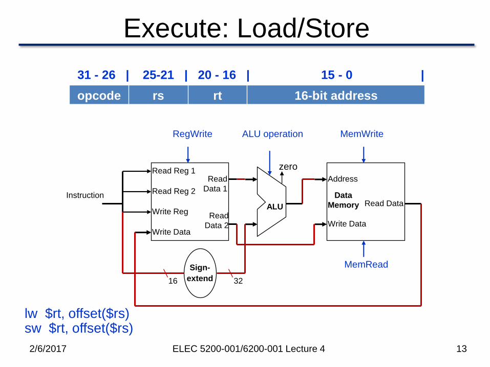
Execute: Load/Store
13
Instruction
Write Data
Read Reg 1
Read Reg 2
Write Reg
Read
Data 1
Read
Data 2
ALU
zero
ALU operationRegWrite
Data
Memory
Address
Write Data
Read Data
Sign-
extend
MemWrite
MemRead
opcode rs rt 16-bit address
31 - 26 | 25-21 | 20 - 16 | 15 - 0 |
lw $rt, offset($rs)sw $rt, offset($rs)
16 32
2/6/2017 ELEC 5200-001/6200-001 Lecture 4

Execute: Branch
14
Instruction
Write Data
Read Reg 1
Read Reg 2
Write Reg
Register File
Read
Data 1
Read
Data 2
AL
U
zero
ALU operation
Ad
d
4 Ad
d
Shift
left 2
PC
Branch
target
address
(To branch
control logic)
32
Sign
Extend16
bne $t0, $t1, Label
beq $t0, $t1, Label
2/6/2017 ELEC 5200-001/6200-001 Lecture 4
15
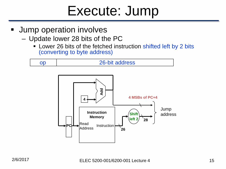
Execute: Jump
Jump operation involves– Update lower 28 bits of the PC
Lower 26 bits of the fetched instruction shifted left by 2 bits (converting to byte address)
Read
AddressInstruction
Instruction
Memory
Ad
d
PC
4
Shift
left 2
26
28
Jump
address
4 MSBs of PC+4
op 26-bit address
2/6/2017 ELEC 5200-001/6200-001 Lecture 4

Assembling Datapath
Assemble the datapath segments
– Add control lines and multiplexors as needed
Single cycle design – fetch, decode and execute each instructions all in one clock cycle
– No datapath resource can be used more than once per instruction
Must be duplicated if needed (e.g., separate Instruction Memory and Data Memory, several adders)
– Multiplexors needed at the input of shared elements with control lines to do the selection
– Write signals to control writing to the Register File and Data Memory
– Cycle time is determined by length of the longest path
162/6/2017 ELEC 5200-001/6200-001 Lecture 4

Instr
[15-11]
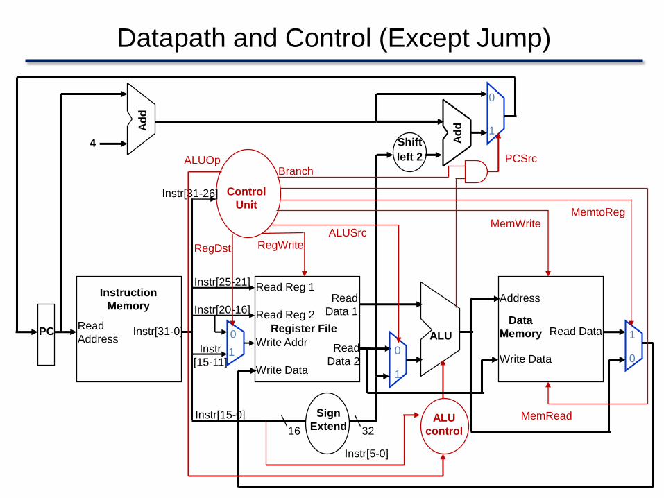
Datapath (Except Jump)
Read
AddressInstr[31-0]
Instruction
Memory
Ad
d
PC
4
Write Data
Read Reg 1
Read Reg 2
Write Addr
Register File
Read
Data 1
Read
Data 2
ALU
RegWrite
Data
Memory
Address
Write Data
Read Data
MemWrite
MemReadSign
Extend16 32
MemtoReg
ALUSrc
Shift
left 2
Ad
d
PCSrc
RegDst
ALU
control
1
1
1
0
00
0
1
Instr[5-0]
Instr[15-0]
Instr[25-21]
Instr[20-16]
Control
UnitInstr[31-26]
zero
ALUOp
Instr
[15-11]
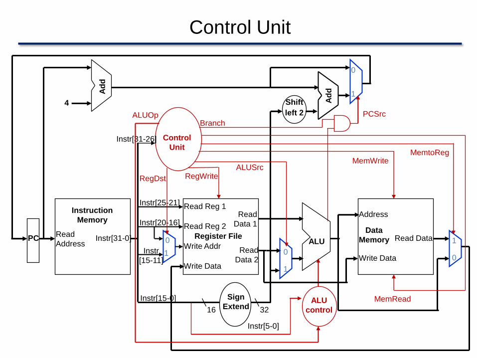
Datapath and Control (Except Jump)
Read
AddressInstr[31-0]
Instruction
Memory
Ad
d
PC
4
Write Data
Read Reg 1
Read Reg 2
Write Addr
Register File
Read
Data 1
Read
Data 2
ALU
RegWrite
Data
Memory
Address
Write Data
Read Data
MemWrite
MemReadSign
Extend16 32
MemtoReg
ALUSrc
Shift
left 2
Ad
d
PCSrc
RegDst
ALU
control
1
1
1
0
00
0
1
Instr[5-0]
Instr[15-0]
Instr[25-21]
Instr[20-16]
Control
UnitInstr[31-26]
ALUOpBranch

Arithmetic Logic Unit (ALU)
2/6/2017 ELEC 5200-001/6200-001 Lecture 4 19
ALU
4
zero
result
overflow
Operation
select
from control
Operation select ALU function
0000 AND
0001 OR
0010 Add
0110 Subtract
0111 Set on less than
1100 NOR
zero = 1, when all bits of result are 0
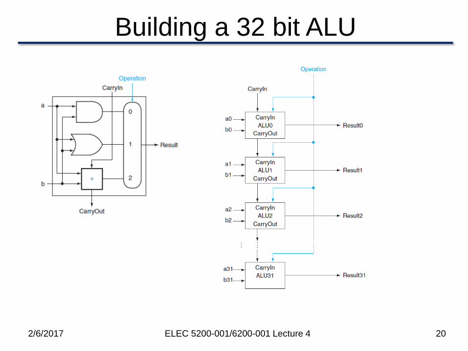
Building a 32 bit ALU
2/6/2017 ELEC 5200-001/6200-001 Lecture 4 20

1-Bit ALU: AND, OR, ADD, SUB, NOR
2/6/2017 ELEC 5200-001/6200-001 Lecture 4 21
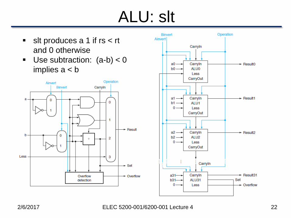
ALU: slt
2/6/2017 ELEC 5200-001/6200-001 Lecture 4 22
slt produces a 1 if rs < rt
and 0 otherwise
Use subtraction: (a-b) < 0
implies a < b

ALU: Branch
2/6/2017 ELEC 5200-001/6200-001 Lecture 4 23

ALU Control ALU Control Lines Function
0000 AND
0001 OR
0010 add
0110 subtract
0111 set on less than
1100 NOR
2/6/2017 ELEC 5200-001/6200-001 Lecture 4 24
Single-Cycle Processor
Simplified MIPS - Control

Datapath and Control (Except Jump)
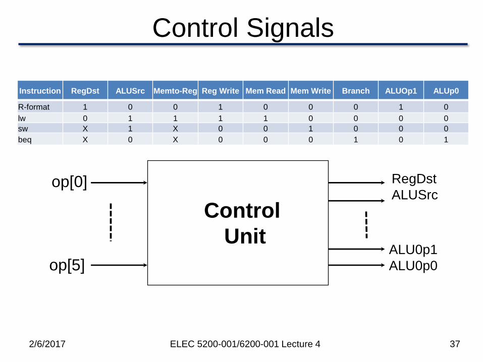
Instruction RegDst ALUSrc Memto-Reg Reg Write Mem Read Mem Write Branch ALUOp1 ALUp0
R-format 1 0 0 1 0 0 0 1 0
lw 0 1 1 1 1 0 0 0 0
sw X 1 X 0 0 1 0 0 0
beq X 0 X 0 0 0 1 0 1

ALU Control Load and store word instructions,
– ALU computes the target memory address by addition– Base address + displacement
Base register + sign_ext(Imm16)
R-type instructions– ALU performs one of the following 5 actions depending on the
value of the 6-bit “funct” field– AND, OR, subtract, add, set on less than
Branch– ALU performs a subtraction– Check the output “ZERO”
We can use 2 bits of opcode (Instr[31:26]) as ALUop to distinguish the above 3 types of instructions– lw/sw (00), beq (01), R-type (10)– Note that the binary encoding (11) is not used
272/6/2017 ELEC 5200-001/6200-001 Lecture 4

Recall: ALU Control Inputs
4 bits required for ALU control inputs, ALUctr
28
Remember this in ALU design?
0000 = and
0001 = or
0010 = add
0110 = subtract
0111 = slt
1100 = NOR
Main
Control
op
6 ?funct
2
6ALUop
ALUctr
4To ALU
functopcode
2/6/2017 ELEC 5200-001/6200-001 Lecture 4
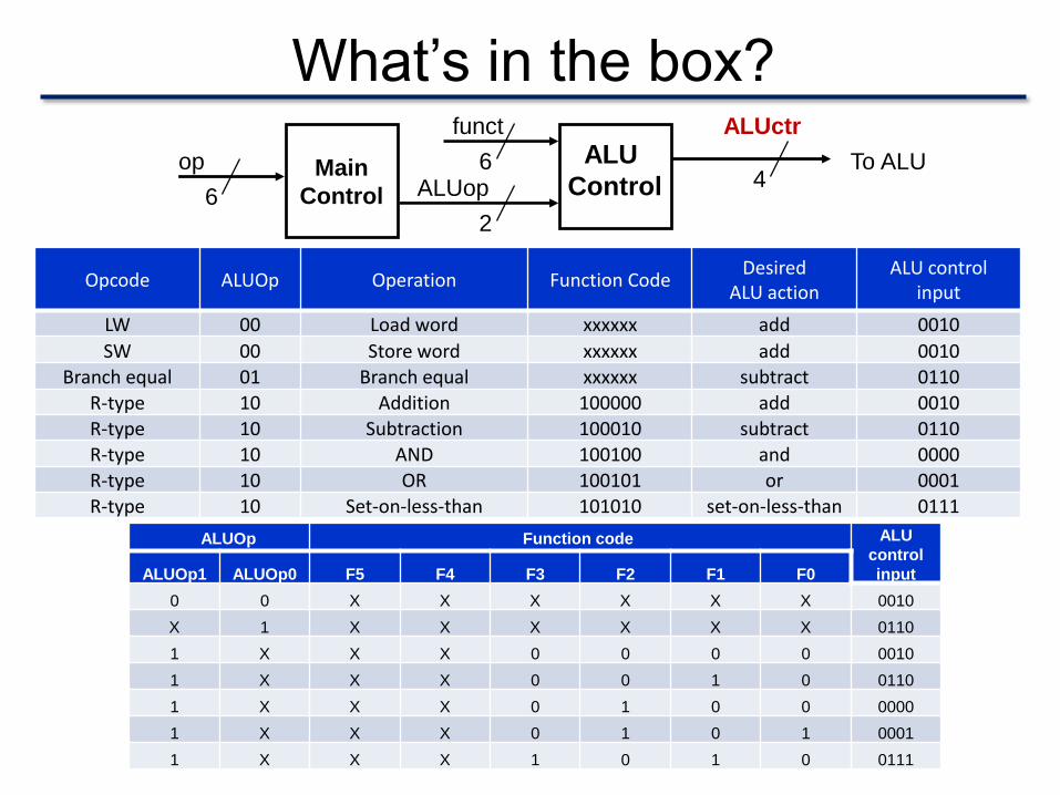
What’s in the box?
Main
Control
op
6
ALU
Control
funct
2
6ALUop
ALUctr
4To ALU
Opcode ALUOp Operation Function CodeDesired
ALU actionALU control
input
LW 00 Load word xxxxxx add 0010
SW 00 Store word xxxxxx add 0010Branch equal 01 Branch equal xxxxxx subtract 0110
R-type 10 Addition 100000 add 0010
R-type 10 Subtraction 100010 subtract 0110
R-type 10 AND 100100 and 0000
R-type 10 OR 100101 or 0001
R-type 10 Set-on-less-than 101010 set-on-less-than 0111
ALUOp Function code ALU
control
inputALUOp1 ALUOp0 F5 F4 F3 F2 F1 F0
0 0 X X X X X X 0010
X 1 X X X X X X 0110
1 X X X 0 0 0 0 0010
1 X X X 0 0 1 0 0110
1 X X X 0 1 0 0 0000
1 X X X 0 1 0 1 0001
1 X X X 1 0 1 0 0111
Instr
[15-11]
Control Unit
Read
AddressInstr[31-0]
Instruction
Memory
Ad
d
PC
4
Write Data
Read Reg 1
Read Reg 2
Write Addr
Register File
Read
Data 1
Read
Data 2
ALU
RegWrite
Data
Memory
Address
Write Data
Read Data
MemWrite
MemReadSign
Extend16 32
MemtoReg
ALUSrc
Shift
left 2
Ad
d
PCSrc
RegDst
ALU
control
1
1
1
0
00
0
1
Instr[5-0]
Instr[15-0]
Instr[25-21]
Instr[20-16]
Control
UnitInstr[31-26]
ALUOpBranch
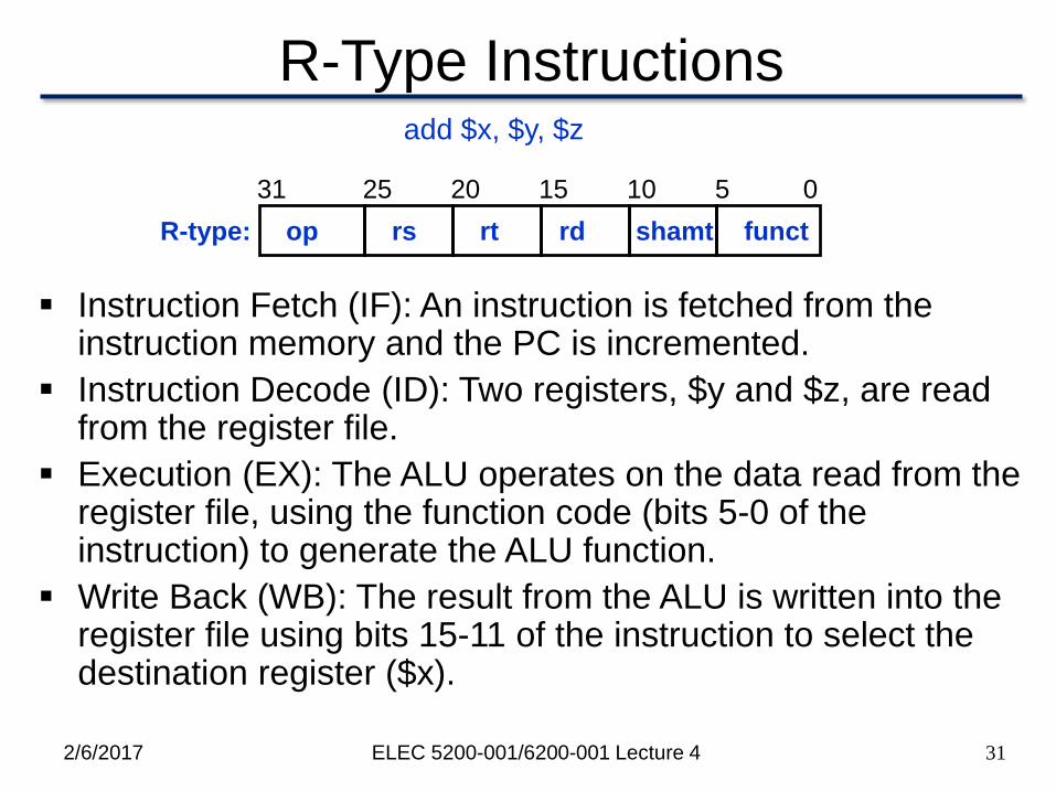
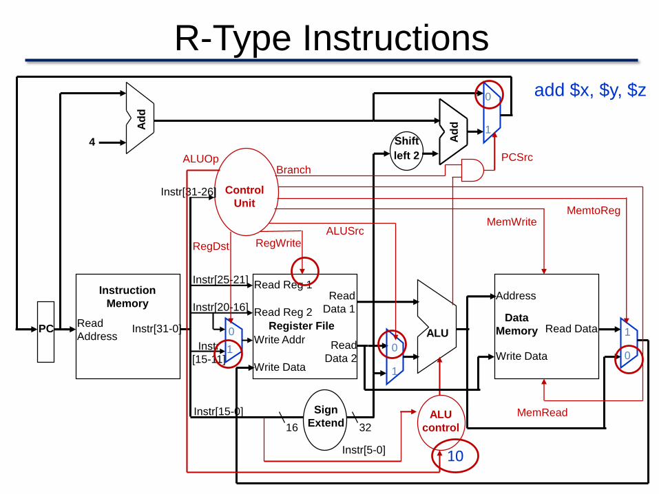
R-Type Instructions
Instruction Fetch (IF): An instruction is fetched from the instruction memory and the PC is incremented.
Instruction Decode (ID): Two registers, $y and $z, are read from the register file.
Execution (EX): The ALU operates on the data read from the register file, using the function code (bits 5-0 of the instruction) to generate the ALU function.
Write Back (WB): The result from the ALU is written into the register file using bits 15-11 of the instruction to select the destination register ($x).
31
R-type: op rs rt rd functshamt
add $x, $y, $z
31 25 20 15 5 010
2/6/2017 ELEC 5200-001/6200-001 Lecture 4
Instr
[15-11]
Read
AddressInstr[31-0]
Instruction
Memory
Ad
d
PC
4
Write Data
Read Reg 1
Read Reg 2
Write Addr
Register File
Read
Data 1
Read
Data 2
ALU
RegWrite
Data
Memory
Address
Write Data
Read Data
MemWrite
MemReadSign
Extend16 32
MemtoReg
ALUSrc
Shift
left 2
Ad
d
PCSrc
RegDst
ALU
control
1
1
1
0
00
0
1
Instr[5-0]
Instr[15-0]
Instr[25-21]
Instr[20-16]
Control
UnitInstr[31-26]
ALUOpBranch
R-Type Instructions
10
add $x, $y, $z

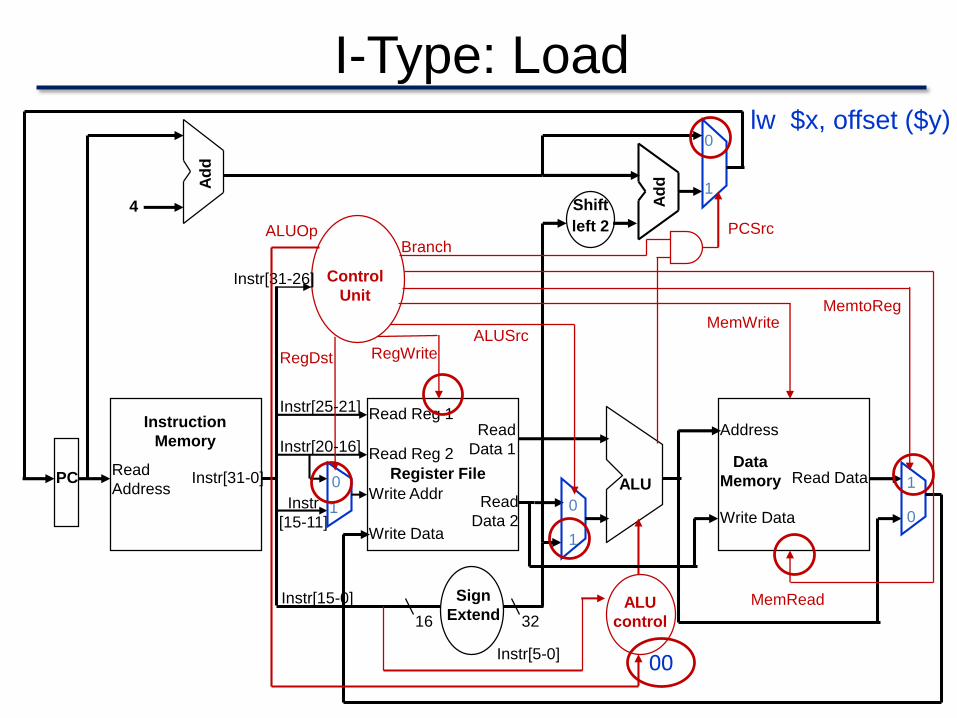
I-Type: Load
Instruction Fetch (IF): An instruction is fetched from the instruction memory and the PC is incremented.
Instruction Decode (ID): A register ($y) value is read from the register file.
Address Calculation (EX): The ALU computes the sum of the value read from the register file and the sign-extended lower 16 bits of the instruction (offset).
Memory Operation (MEM): The sum from the ALU is used as the address for the data memory.
Write Back (WB): The data from the memory unit is written into the register file; the register destination is given by bits 20-16 of the instruction ($x).
33
I-type: op rs rt
lw $x, offset ($y)
31 25 20 15 0
offset
2/6/2017 ELEC 5200-001/6200-001 Lecture 4
Instr
[15-11]
Read
AddressInstr[31-0]
Instruction
Memory
Ad
d
PC
4
Write Data
Read Reg 1
Read Reg 2
Write Addr
Register File
Read
Data 1
Read
Data 2
ALU
RegWrite
Data
Memory
Address
Write Data
Read Data
MemWrite
MemReadSign
Extend16 32
MemtoReg
ALUSrc
Shift
left 2
Ad
d
PCSrc
RegDst
ALU
control
1
1
1
0
00
0
1
Instr[5-0]
Instr[15-0]
Instr[25-21]
Instr[20-16]
Control
UnitInstr[31-26]
ALUOpBranch
I-Type: Load
00
lw $x, offset ($y)
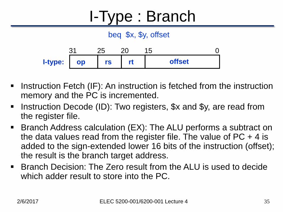
I-Type : Branch
Instruction Fetch (IF): An instruction is fetched from the instruction memory and the PC is incremented.
Instruction Decode (ID): Two registers, $x and $y, are read from the register file.
Branch Address calculation (EX): The ALU performs a subtract on the data values read from the register file. The value of PC + 4 is added to the sign-extended lower 16 bits of the instruction (offset); the result is the branch target address.
Branch Decision: The Zero result from the ALU is used to decide which adder result to store into the PC.
35
I-type: op rs rt
beq $x, $y, offset
31 25 20 15 0
offset
2/6/2017 ELEC 5200-001/6200-001 Lecture 4
Instr
[15-11]
Read
AddressInstr[31-0]
Instruction
Memory
Ad
d
PC
4
Write Data
Read Reg 1
Read Reg 2
Write Addr
Register File
Read
Data 1
Read
Data 2
ALU
RegWrite
Data
Memory
Address
Write Data
Read Data
MemWrite
MemReadSign
Extend16 32
MemtoReg
ALUSrc
Shift
left 2
Ad
d
PCSrc
RegDst
ALU
control
1
1
1
0
00
0
1
Instr[5-0]
Instr[15-0]
Instr[25-21]
Instr[20-16]
Control
UnitInstr[31-26]
ALUOpBranch
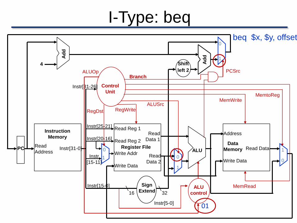
I-Type: beq
01
beq $x, $y, offset
Control Signals
2/6/2017 ELEC 5200-001/6200-001 Lecture 4 37
Instruction RegDst ALUSrc Memto-Reg Reg Write Mem Read Mem Write Branch ALUOp1 ALUp0
R-format 1 0 0 1 0 0 0 1 0
lw 0 1 1 1 1 0 0 0 0
sw X 1 X 0 0 1 0 0 0
beq X 0 X 0 0 0 1 0 1
op[0]
op[5]
Control
Unit
RegDst
ALUSrc
ALU0p1
ALU0p0

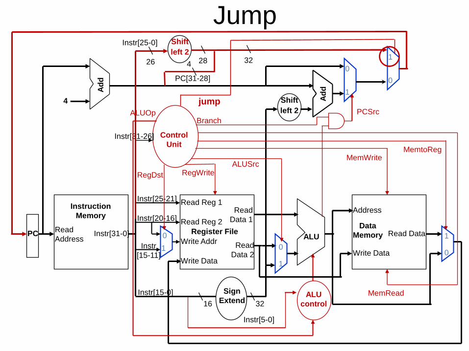
Adding “jump” hardware
38
op 26-bit address
PC
4
32
26
32
00
Low order 26 bits of the jump instruction
Note: the 26-bit address is a “word” address
Must be multiplied by 4 to obtain the “byte” address, i.e. shift-left-by 2
PC[31:28] or
PC+4[31:28]?
2/6/2017 ELEC 5200-001/6200-001 Lecture 4
Instr
[15-11]
Jump
Read
AddressInstr[31-0]
Instruction
Memory
Ad
d
PC
4
Write Data
Read Reg 1
Read Reg 2
Write Addr
Register File
Read
Data 1
Read
Data 2
ALU
RegWrite
Data
Memory
Address
Write Data
Read Data
MemWrite
MemReadSign
Extend16 32
MemtoReg
ALUSrc
Shift
left 2
Ad
d
PCSrc
RegDst
ALU
control
1
1
1
0
00
0
1
Instr[5-0]
Instr[15-0]
Instr[25-21]
Instr[20-16]
Control
UnitInstr[31-26]
ALUOpBranch
1
0
Shift
left 2
jump
Instr[25-0]
26 28
PC[31-28]
432
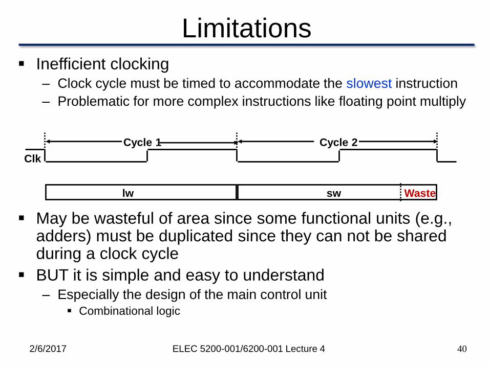
Limitations
Inefficient clocking– Clock cycle must be timed to accommodate the slowest instruction
– Problematic for more complex instructions like floating point multiply
May be wasteful of area since some functional units (e.g., adders) must be duplicated since they can not be shared during a clock cycle
BUT it is simple and easy to understand– Especially the design of the main control unit
Combinational logic
40
Clk
lw sw Waste
Cycle 1 Cycle 2
2/6/2017 ELEC 5200-001/6200-001 Lecture 4

Critical Path (Load)
Register file and ideal memory:
– The CLK input is a factor ONLY during write
operation
– During read operation, behave as combinational
logic:
Address valid => Output valid after “access
time.” (i.e. delay)
Critical Path = PC’s Clk-to-Q + Instruction Memory’s Access Time +
Register File’s Access Time + ALU to Perform a 32-bit Add + Data Memory
Access Time + Setup Time for Register File Write + Clock Skew
PC Instruction
Instructionmemory
Data
ALU
Register #
Register #
Register #
Regis
ters
Address
Data
Address
Data Memory
4
Add
Clk
Clk
Clk

Cycle Time
42
Arithmetic & Logical
Load
Store
Branch
Critical Path
IF ID EXE WB
IF ID EXE MEM WB
IF ID EXE MEM
IF ID EXE
2/6/2017 ELEC 5200-001/6200-001 Lecture 4

Multicycle Datapath Approach
Let an instruction take more than 1 clock cycle to complete
– Break up instructions into steps where each step takes a cycle while trying to
Balance the amount of work to be done in each step
Restrict each cycle to use only one major functional unit
– Not every instruction takes the same number of clock cycles
In addition to faster clock rates, multicycle allows functional units that can be used more than once per instruction as long as they are used in different clock cycles, hence
– One memory – but only one memory access per cycle
Recall instruction and data memory in single-cycle processor
– One ALU/adder – but only one ALU operation per cycle
Recall one adder for PC+4 and one ALU/adder for others in single-cycle processor
432/6/2017 ELEC 5200-001/6200-001 Lecture 4

Reducing Cycle Time Cut combinational dependency graph and insert register / latch
Do the same work in two fast cycles, rather than one slow one
44
storage element
Acyclic
Combinational
Logic
storage element
storage element
Acyclic
Combinational
Logic (A)
storage element
storage element
Acyclic
Combinational
Logic (B)
=>
2/6/2017 ELEC 5200-001/6200-001 Lecture 4
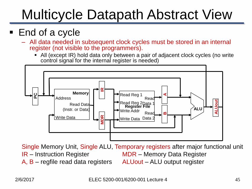
Multicycle Datapath Abstract View
End of a cycle– All data needed in subsequent clock cycles must be stored in an internal
register (not visible to the programmers). All (except IR) hold data only between a pair of adjacent clock cycles (no write
control signal for the internal register is needed)
Single Memory Unit, Single ALU, Temporary registers after major functional unit
IR – Instruction Register MDR – Memory Data Register
A, B – regfile read data registers ALUout – ALU output register
45
Address
Read Data
(Instr. or Data)
Memory
PC
Write Data
Read Reg 1
Read Reg 2
Write AddrRegister File
Read
Data 1
Read
Data 2
ALU
Write Data
IRM
DR
AB A
LU
ou
t
2/6/2017 ELEC 5200-001/6200-001 Lecture 4

Next: Pipelining
https://www.youtube.com/watch?v=IjarLbD9r30
https://www.youtube.com/watch?v=ANXGJe6i3G8
https://www.youtube.com/watch?v=5lp4EbfPAtI