efficiency of logic minimization techniques for
TRANSCRIPT

Efficiency of Logic Minimization Techniques for CryptographicHardware Implementation
Shashank Raghuraman
Thesis submitted to the Faculty of the
Virginia Polytechnic Institute and State University
in partial fulfillment of the requirements for the degree of
Master of Science
in
Computer Engineering
Leyla Nazhandali, Chair
Patrick R Schaumont
Haibo Zeng
June 14, 2019
Blacksburg, Virginia
Keywords: Logic synthesis, Cryptographic hardware, Circuit minimization, Leon-3,
System-on-Chip, Authenticated encryption hardware.
Copyright 2019, Shashank Raghuraman

Efficiency of Logic Minimization Techniques for CryptographicHardware Implementation
Shashank Raghuraman
(ABSTRACT)
With significant research effort being directed towards designing lightweight cryptographic
primitives, logical metrics such as gate count are extensively used in estimating their hard-
ware quality. Specialized logic minimization tools have been built to make use of gate count
as the primary optimization cost function. The first part of this thesis aims to investigate
the effectiveness of such logical metrics in predicting hardware efficiency of corresponding
circuits. Mapping a logical representation onto hardware depends on the standard cell tech-
nology used, and is driven by trade-offs between area, performance, and power. This work
evaluates aforementioned parameters for circuits optimized for gate count, and compares
them with a set of benchmark designs. Extensive analysis is performed over a wide range of
frequencies at multiple levels of abstraction and system integration, to understand the dif-
ferent regions in the solution space where such logic minimization techniques are effective. A
prototype System-on-Chip (SoC) is designed to benchmark the performance of these circuits
on actual hardware. This SoC is built with an aim to include multiple other cryptographic
blocks for analysis of their hardware efficiency. The second part of this thesis analyzes
the overhead involved in integrating selected authenticated encryption ciphers onto an SoC,
and explores different design alternatives for the same. Overall, this thesis is intended to
serve as a comprehensive guideline on hardware factors that can be overlooked, but must
be considered during logical-to-physical mapping and during the integration of standalone
cryptographic blocks onto a complete system.

Efficiency of Logic Minimization Techniques for CryptographicHardware Implementation
Shashank Raghuraman
(GENERAL AUDIENCE ABSTRACT)
The proliferation of embedded smart devices for the Internet-of-Things necessitates a con-
stant search for smaller and power-efficient hardware. The need to ensure security of such
devices has been driving extensive research on lightweight cryptography, which focuses on
minimizing the logic footprint of cryptographic hardware primitives. Different designs are
optimized, evaluated, and compared based on the number of gates required to express them
at a logical level of abstraction. The expectation is that circuits requiring fewer gates to
represent their logic will be smaller and more efficient on hardware. However, converting a
logical representation into a hardware circuit, known as “synthesis”, is not trivial. The logic
is mapped to a “library” of hardware cells, and one of many possible solutions for a function
is selected - a process driven by trade-offs between area, speed, and power consumption on
hardware. Our work studies the impact of synthesis on logical circuits with minimized gate
count. We evaluate the hardware quality of such circuits by comparing them with that of
benchmark designs over a range of speeds. We wish to answer questions such as “At what
speeds do logical metrics rightly predict area- and power-efficiency?”, and “What impact
does this have after integrating cryptographic primitives onto a complete system?”. As part
of this effort, we build a System-on-Chip in order to observe the efficiency of these circuits
on actual hardware. This chip also includes recently developed ciphers for authenticated en-
cryption. The second part of this thesis explores different ways of integrating these ciphers
onto a system, to understand their effect on the ciphers’ compactness and performance. Our
overarching aim is to provide a suitable reference on how synthesis and system integration
affect the hardware quality of cryptographic blocks, for future research in this area.

Dedication
To my family.
iv

Acknowledgments
First and foremost, I thank my parents, brother, and everyone else in my family back home
in India for their constant support and encouragement throughout my graduate studies. I
am indebted to my uncle, Aravind Srinivasan, and my friend, Lakshman Maalolan, both of
whose presence and positivity were an integral part of my education at Virginia Tech. I offer
my gratitude to my advisor Dr. Leyla Nazhandali, whose invaluable guidance and faith in
me were my biggest sources of motivation. I have drawn inspiration from her approachable
and good-natured mentorship, academic expertise, and skills in presentation, which I believe,
have moulded me into a better professional. I must thank Dr. Patrick Schaumont for his
ideas, insights, and critique through the course of our collaborative work. I will always aspire
to acquire his ability to articulate complex ideas and findings in the simplest possible manner.
I also thank Dr. Nazhandali, Dr. Schaumont, and Dr. Haibo Zeng for having agreed to be part
of my Masters advisory committee. I thank NIST for having funded our project, and Dr. René
Peralta for his prompt responses to our queries. I wish to acknowledge Pantea Kiaei for her
dedication to our shared project, and the members and alumni of Secure Embedded Systems
Lab - with special mention to Archanaa S Krishnan, Tarun Kathuria, Daniel Dinu, and
Chinmay Deshpande - for their cheerful companionship and transfer of knowledge. During
my Masters, I had the opportunity of interning at Qualcomm in Boulder. I thank everyone in
that team - in particular, Curt Musfeldt, Brian Steele, and Karthi Subbiah - who made it a
rich learning experience that enhanced my confidence. Finally, I express my gratitude to my
friends Subramaniam Mahadevan, Swati Bhardwaj, and Naresh Vemishetty for their words
of encouragement, and Vamsi Chandra, Shamit Bansal, Omkar Dhande, Abhinuv Pitale,
and Akhil Ahmed for their help and the fun times I spent in Blacksburg.
v
Contents
1 Introduction 1
1.1 Motivation . . . . . . . . . . . . . . . . . . . . . . . . . . . . . . . . . . . . . 1
1.2 Relevant Preliminaries . . . . . . . . . . . . . . . . . . . . . . . . . . . . . . 5
1.2.1 Digital Logic synthesis . . . . . . . . . . . . . . . . . . . . . . . . . . 5
1.2.2 Low Gate-Count (LGC) Synthesis Tool . . . . . . . . . . . . . . . . . 9
1.3 Our Contributions . . . . . . . . . . . . . . . . . . . . . . . . . . . . . . . . 10
1.4 Attribution . . . . . . . . . . . . . . . . . . . . . . . . . . . . . . . . . . . . 11
1.5 Thesis Organization . . . . . . . . . . . . . . . . . . . . . . . . . . . . . . . 12
2 Cryptographic Benchmark Selection and Experimental Methodology 13
2.1 Benchmark Designs . . . . . . . . . . . . . . . . . . . . . . . . . . . . . . . . 13
2.1.1 AES SBox . . . . . . . . . . . . . . . . . . . . . . . . . . . . . . . . . 14
2.1.2 Binary Polynomial Multiplication . . . . . . . . . . . . . . . . . . . . 15
2.1.3 Galois Field Multiplication . . . . . . . . . . . . . . . . . . . . . . . 17
2.1.4 Galois Field Inversion . . . . . . . . . . . . . . . . . . . . . . . . . . 19
2.1.5 Reed-Solomon Encoder . . . . . . . . . . . . . . . . . . . . . . . . . . 20
2.2 Experimental Setup . . . . . . . . . . . . . . . . . . . . . . . . . . . . . . . . 22
2.2.1 Integration of SLPs into ASIC design flow . . . . . . . . . . . . . . . 22
vi
2.2.2 Design alternatives for LGC designs . . . . . . . . . . . . . . . . . . 24
2.2.3 Standard cell library choices . . . . . . . . . . . . . . . . . . . . . . . 25
3 Experimental results of logic synthesis of benchmark designs 26
3.1 Combinatorial logic synthesis results . . . . . . . . . . . . . . . . . . . . . . 26
3.1.1 Technology-independent evaluation . . . . . . . . . . . . . . . . . . . 26
3.1.2 Post-synthesis analysis . . . . . . . . . . . . . . . . . . . . . . . . . . 29
3.2 Integrated Design Examples . . . . . . . . . . . . . . . . . . . . . . . . . . . 47
3.2.1 Comparison of AES designs with different SBox circuits . . . . . . . 47
3.2.2 Reed-Solomon Encoder . . . . . . . . . . . . . . . . . . . . . . . . . . 52
3.3 Effect of physical design . . . . . . . . . . . . . . . . . . . . . . . . . . . . . 56
3.4 Connection between abstract and technology-dependent quality metrics . . . 58
4 Design of prototype ASIC 63
4.1 Design Rationale . . . . . . . . . . . . . . . . . . . . . . . . . . . . . . . . . 63
4.2 SoC Architecture . . . . . . . . . . . . . . . . . . . . . . . . . . . . . . . . . 64
4.2.1 Memory-mapped coprocessors on NISTCHIP . . . . . . . . . . . . . 66
4.2.2 NISTCOMB coprocessor: Design and Programming model . . . . . . 69
4.3 NISTCHIP ASIC Design . . . . . . . . . . . . . . . . . . . . . . . . . . . . . 70
4.3.1 Logic synthesis of NISTCHIP . . . . . . . . . . . . . . . . . . . . . . 71
4.3.2 NISTCHIP Physical Design flow . . . . . . . . . . . . . . . . . . . . 72
vii

4.3.3 The final ASIC layout . . . . . . . . . . . . . . . . . . . . . . . . . . 76
4.4 Post-layout results . . . . . . . . . . . . . . . . . . . . . . . . . . . . . . . . 77
4.4.1 Area . . . . . . . . . . . . . . . . . . . . . . . . . . . . . . . . . . . . 77
4.4.2 Power Consumption . . . . . . . . . . . . . . . . . . . . . . . . . . . 77
5 Impact of SoC integration on Authenticated Encryption Ciphers 81
5.1 Introduction . . . . . . . . . . . . . . . . . . . . . . . . . . . . . . . . . . . . 81
5.2 Relevant Background . . . . . . . . . . . . . . . . . . . . . . . . . . . . . . . 83
5.2.1 ACORN . . . . . . . . . . . . . . . . . . . . . . . . . . . . . . . . . . 83
5.2.2 AEGIS . . . . . . . . . . . . . . . . . . . . . . . . . . . . . . . . . . 85
5.2.3 MORUS . . . . . . . . . . . . . . . . . . . . . . . . . . . . . . . . . . 87
5.3 Design alternatives for SoC integration . . . . . . . . . . . . . . . . . . . . . 87
5.3.1 An intuitive and convenient wrapper design - FIFOs at the input and
output . . . . . . . . . . . . . . . . . . . . . . . . . . . . . . . . . . . 88
5.3.2 Reducing wrapper overhead - FIFO only at the output . . . . . . . . 90
5.3.3 Lightweight integration - no FIFOs in the wrapper . . . . . . . . . . 91
5.3.4 Direct Memory Access (DMA) for increased throughput . . . . . . . 93
5.4 Evaluation Methodology . . . . . . . . . . . . . . . . . . . . . . . . . . . . . 93
5.4.1 Studying Area and Power . . . . . . . . . . . . . . . . . . . . . . . . 94
5.4.2 Performance Analysis . . . . . . . . . . . . . . . . . . . . . . . . . . 94
5.5 Observations and Results . . . . . . . . . . . . . . . . . . . . . . . . . . . . 95
viii

5.5.1 ACORN-32 . . . . . . . . . . . . . . . . . . . . . . . . . . . . . . . . 96
5.5.2 ACORN-8 . . . . . . . . . . . . . . . . . . . . . . . . . . . . . . . . . 103
5.5.3 AEGIS-128L . . . . . . . . . . . . . . . . . . . . . . . . . . . . . . . 105
5.5.4 MORUS . . . . . . . . . . . . . . . . . . . . . . . . . . . . . . . . . . 108
5.6 Conclusion . . . . . . . . . . . . . . . . . . . . . . . . . . . . . . . . . . . . . 110
6 Conclusion 113
Bibliography 114
Appendices 121
Appendix A Additional results for logic synthesis of LGC circuits 122
Appendix B NISTCHIP Memory Map 127
Appendix C Additional results for SoC integration of AEAD Ciphers 130
ix

Chapter 1
Introduction
1.1 Motivation
The necessity for cryptographic hardware with small logic footprint, high performance, and
low power consumption has become paramount with the growing popularity and usage of
the Internet-of-Things (IoT). High-volume applications and lightweight embedded devices
primarily require reduction in silicon area. On the other hand, shared applications in the
cloud that deal with a large number of users need to support bulk data processing, and
hence require high-performance cryptography [28]. Both of these common requirements have
eventually lead to research that predominantly focuses on minimizing the logic complexity
of cryptographic designs.
Techniques to improve the quality of hardware implementations exist at all possible levels
of abstraction - from algorithms right down to semiconductor technology. The focus of this
work is to study the effects of optimization between algorithm-level and device-level, widely
characterized as logic synthesis. We consider popularly-used implementations for standard
known cryptographic algorithms, making use of vendor-provided gate-level primitives for
their hardware realization. We therefore do not focus on minimization techniques at high-
level algorithm formulation or the optimization of VLSI design layout. This work focuses
on minimization performed at the level of logical representation of cryptographic primitives.
We analyze the impact of realizing these logic-minimized designs on actual hardware through
1

2 Chapter 1. Introduction
an implementation flow that is adopted as a common standard.
With regard to obtaining compactness, low power, and high performance on hardware, it is
natural to expect that logic reduction at the architectural level translates into desired hard-
ware efficiency. Fewer logic operations are intuitively assumed to directly produce smaller
hardware, and indirectly affect power consumption [27]. Similarly, a design with fewer lev-
els of logic operations is expected to yield a faster circuit on hardware. For cryptographic
logic designers at this relatively high level of abstraction, it makes sense to focus on the
best available metric that quantifies compactness - gate count. This has naturally gained
widespread usage through the years as an important indicator of the “efficiency” of cryp-
tographic logic designs, and more importantly, in comparing one design alternative with
another [5, 9, 12, 15, 20, 26]. Optimization tools driven by gate count and/or depth as
their cost functions have been developed for different classes of functions [8, 11, 17, 22, 47].
Some works discuss the expected circuit speed in terms of its logical depth before synthesis
[16, 24, 27, 37, 39], or as an estimate obtained from a library, depending on logical complexity
[32].
An important point that needs to be considered is that converting the logical representation
of a design into cells of a hardware library is not a trivial task. These hardware cells come
with diverse functionality and sizes. Therefore, there does not exist a unique mapping from
a design with low gate count to a larger set of library cells. Determining an optimal solution
from these is driven by constraints specified by the user. For example, a simple and direct
mapping of a logic-minimized design onto corresponding hardware cells is bound to give the
smallest solution. However, placing a tight delay requirement on such a design necessitates
searching for an alternative solution through a different logic mapping and bigger cells. This
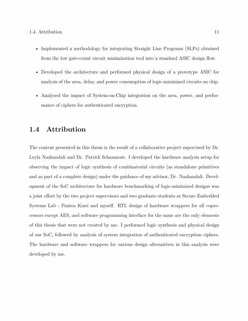
naturally increases the area of the circuit. Figure 1.1 shows a typical plot of area against
delay of designs synthesized by a constraint-driven tool. Achieving a solution that is better
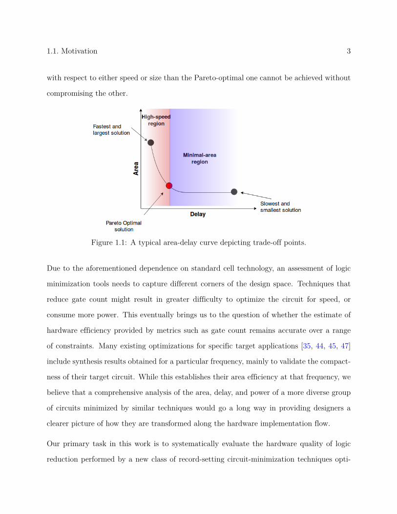
1.1. Motivation 3
with respect to either speed or size than the Pareto-optimal one cannot be achieved without
compromising the other.
Figure 1.1: A typical area-delay curve depicting trade-off points.
Due to the aforementioned dependence on standard cell technology, an assessment of logic
minimization tools needs to capture different corners of the design space. Techniques that
reduce gate count might result in greater difficulty to optimize the circuit for speed, or
consume more power. This eventually brings us to the question of whether the estimate of
hardware efficiency provided by metrics such as gate count remains accurate over a range
of constraints. Many existing optimizations for specific target applications [35, 44, 45, 47]
include synthesis results obtained for a particular frequency, mainly to validate the compact-
ness of their target circuit. While this establishes their area efficiency at that frequency, we
believe that a comprehensive analysis of the area, delay, and power of a more diverse group
of circuits minimized by similar techniques would go a long way in providing designers a
clearer picture of how they are transformed along the hardware implementation flow.
Our primary task in this work is to systematically evaluate the hardware quality of logic
reduction performed by a new class of record-setting circuit-minimization techniques opti-

4 Chapter 1. Introduction
mized for reducing gate-count [8, 11, 41]. This Low Gate-Count (LGC) tool primarily focuses
on reducing multiplicative complexity, minimizing the number of XOR operations, and if
desired, reducing the depth of combinatorial circuits. These techniques have produced some
of the smallest known combinatorial primitives of cryptographic importance [9, 12]. Our
aim is to perform a comprehensive hardware efficiency analysis of these circuits over a range
of constraints covering various trade-off points over the design trajectory. Considering that
these tools have been optimized for a large class of combinatorial cryptographic circuits, we
believe this analysis provides significant insight into the overall hardware efficiency of such
methodologies, and helps identify specific regions in the design space where these circuits
are efficient. Specifically, we attempt to address the following points:
• Trade-off regions: Owing to the conflicting nature of hardware quality metrics, it is
conceivable that synthesis methods that are superior in one metric are inferior in another.
There is rarely a case of “one-size-fits-all” with regard to logic synthesis. It is therefore
important to identify these regions of the solution space to get a better assessment of
when LGC tools are preferable over other alternatives.
• Suitability towards wide range of functions: Similar to the previous point, there
is a possibility of one synthesis method outperforming another for a particular class of
logic functions, and not so for a different class. The same optimization strategy can
affect different functions in different ways depending on their complexity and structural
properties. Since the LGC tool is shown to be applicable to a wide range of circuits, it is
of interest to analyze the consistency of hardware efficiency over different logic functions.
• Scaling of hardware metrics: As logic synthesis is a constraint-driven process, a
circuit that is better at one operating frequency can be worse at a higher frequency. In
other words, different circuits do not scale in the same manner with respect to their

1.2. Relevant Preliminaries 5
design quality. We wish to observe how area and power scale with design constraints and
complexity. This eventually produces plots similar to Figure 1.1 that help understand the
optimal regions of operation for different synthesis schemes.
To evaluate the LGC tool, we compare the quality of designs it creates, against those pro-
duced by commercial tools, as well as other existing optimization techniques for the same
logic functions. These comparisons are performed at different levels of abstraction in the
implementation flow of an Application Specific Integrated Circuit (ASIC). In addition to
evaluating the quality of combinatorial primitives as standalone blocks, we include analysis
of an overall system design incorporating these primitives. This is aimed at demonstrating
their suitability in a practical setting. We design a prototype ASIC that includes some of
these cryptographic primitives as part of our effort in evaluating their efficiency on actual
hardware.
1.2 Relevant Preliminaries
1.2.1 Digital Logic synthesis
An algorithm can be described as a logic function in multiple ways - a high-level look-up table
specifying its input-output relation, using expressions with Boolean operators representing
logic gates, or through behavioral description in a Hardware Description Language (HDL)
such as Verilog, VHDL, SystemVerilog, etc. Realizing such a description as a circuit on
hardware involves providing it to a logic synthesis tool along with a collection of standard
cells, known as a standard cell library or technology library. Such a library, generally provided
by a commercial vendor, consists of hardware primitives belonging to a particular technology
represented by dimensions and other properties of the transistors used to construct them.
6 Chapter 1. Introduction
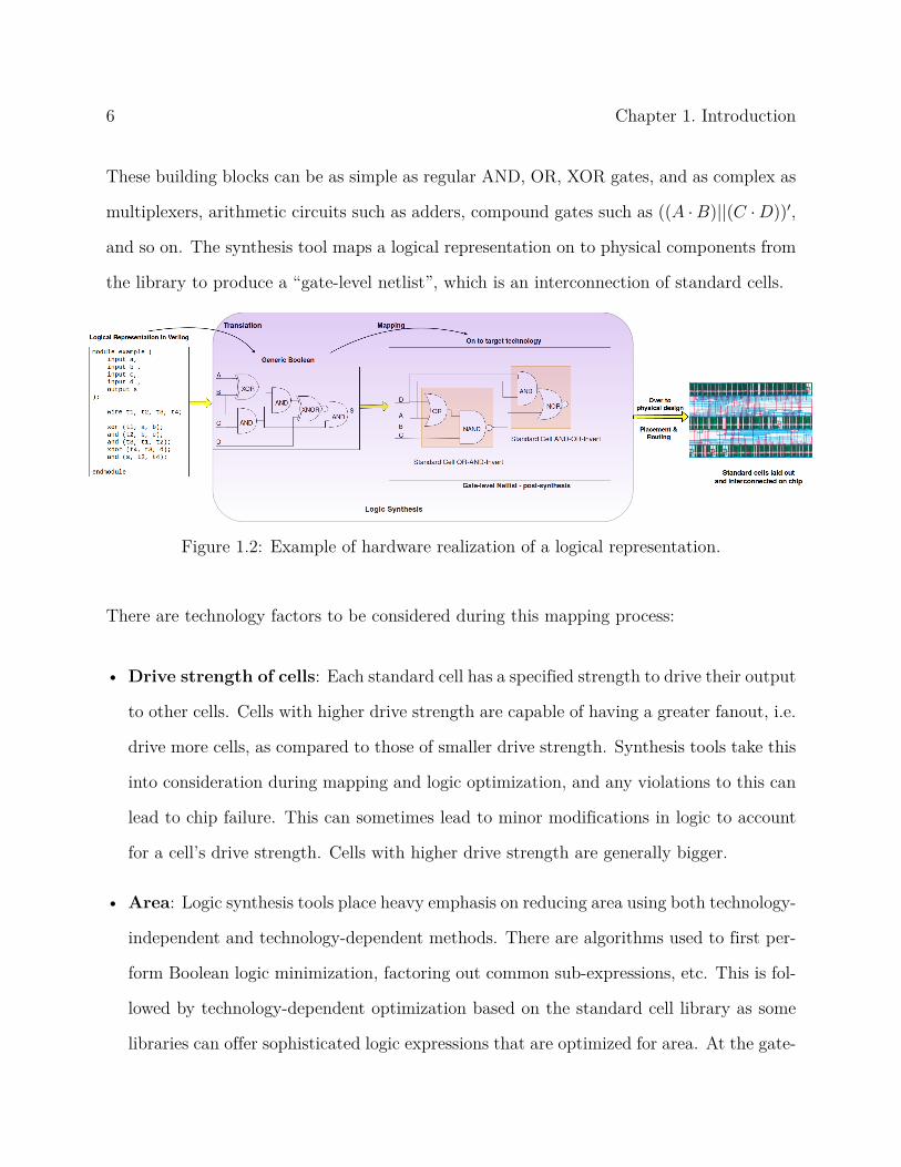
These building blocks can be as simple as regular AND, OR, XOR gates, and as complex as
multiplexers, arithmetic circuits such as adders, compound gates such as ((A ·B)||(C ·D))′,
and so on. The synthesis tool maps a logical representation on to physical components from
the library to produce a “gate-level netlist”, which is an interconnection of standard cells.
Figure 1.2: Example of hardware realization of a logical representation.
There are technology factors to be considered during this mapping process:
• Drive strength of cells: Each standard cell has a specified strength to drive their output
to other cells. Cells with higher drive strength are capable of having a greater fanout, i.e.
drive more cells, as compared to those of smaller drive strength. Synthesis tools take this
into consideration during mapping and logic optimization, and any violations to this can
lead to chip failure. This can sometimes lead to minor modifications in logic to account
for a cell’s drive strength. Cells with higher drive strength are generally bigger.
• Area: Logic synthesis tools place heavy emphasis on reducing area using both technology-
independent and technology-dependent methods. There are algorithms used to first per-
form Boolean logic minimization, factoring out common sub-expressions, etc. This is fol-
lowed by technology-dependent optimization based on the standard cell library as some
libraries can offer sophisticated logic expressions that are optimized for area. At the gate-

1.2. Relevant Preliminaries 7
level, cells with smaller drive strength can be used in places with small fanout to save
area.
Figure 1.3: Area optimization during logic synthesis
• Delay: The output of each cell incurs a non-zero delay before it goes to the correct logic
value. In a combinatorial circuit with many levels of gates, the delay of each gate and
the interconnection between gates add up to form the total delay of that combinatorial
circuit. Designers often specify the desired speed of the circuit, which places a limitation
on the maximum delay of that circuit. In addition, flip flops in the standard cell library
have a setup time requirement which again places a limit on the maximum delay of a path
between two flip flops. Synthesis tools perform logic optimization for minimizing delay.
This leads to modifications in the type(s) of cells used, since there could be cells that are
faster and hence better alternatives to a direct mapping of the circuit that is logically
described.
• Power: Cells that have low power consumption are ideally preferred, but they have
a direct impact on the cell delay. For instance, faster cells often consume more power.
Delay is generally prioritized over power since failure to meet timing can cause unintended
behavior.
• Design rules: These are rules specified by the technology vendor, failure to meet which
can lead to design failure. These rules are prioritized over area, delay, and power by
synthesis tools. For example, a cell can have a maximum fanout specified. If this is

8 Chapter 1. Introduction
exceeded in the circuit description, the logic has to be modified in a way that doesn’t lead
to further design rule violations, even if it entails an increase in area, power, or delay.
Similarly, there are limitations on the maximum capacitance a cell can drive, and the
maximum signal transition time allowed for it to be correctly recognized by the next cell.
Impact of standard cells: The greatest challenge to logic synthesis tools is to find a
sweet spot between what the user requires in terms of area, delay, power, and what the
technology library offers along with its design rules. Synthesis cost functions include all
these constraints, and tools constantly evaluate trade-offs between them. An important
point that needs mention is that there are variations in standard cells with respect to area,
power, and delay, that cannot be overlooked. For example, Figure 1.4 shows a simple example
of the area of commonly used standard cells from two different libraries, normalized to that
of a 2-input NAND gate of the same technology. It is easy to see that XOR and XNOR gates
are significantly bigger than other cells of an equivalent drive strength. Similar observations
can be made for delay and power consumption - they are different for different cells, and
depend on input signal transition and output load.
Gate Type
Area
(Gat
e Eq
.)
0
2
4
6
XOR2
XNOR2AND2
OR2
NAND2NOR2
AOI211
OAI211IN
VMX2
Drive Strength - X1 Drive Strength - X2 Drive Strength - X4
Area of common Standard cells - TSMC 180 nm technology
(a)Gate Type
Area
(Gat
e Eq
.)
0
0.5
1
1.5
2
XOR2 XNOR2 AND2 OR2 NAND2 NOR2 AOI21 OAI21 INV
Drive Strength - X1 Drive Strength - X2 Drive Strength - X4
Area of common Standard cells - SAED 32 nm technology
(b)
Figure 1.4: Area comparison of common 2-input standard cells from (a) TSMC 180 nm, and(b) Synopsys SAED 32/28 nm standard cell libraries.
What this highlights is that a cryptographic LGC circuit dominated by XOR gates cannot

1.2. Relevant Preliminaries 9
be directly assumed to be smaller in hardware than a more abstract representation, just by
virtue of having fewer gates. While differences of many hundreds of gates are likely to be
reflected on hardware, those of the order of few tens of gates are not guaranteed of area
efficiency after synthesis. This again points to an area-delay trade-off. The differences on
hardware depend on heuristics deployed by the synthesis tool to find an optimal mapping and
sizing of cells to meet design requirements. While the starting point could be the smallest
possible representation of the circuit, it is conceivable that the tool sees the need for certain
groups of gates to be replaced with compound gates in the library that better meet timing or
have a higher driving ability. Moreover, when integrated with a bigger design (for example,
when an AES SBox is plugged in between the other steps in an AES round), there are often
cells before and after the combinatorial block we are concerned with. This imposes further
delay constraints and can provide scope for logic optimization across logical boundaries as
shown in Figure 1.5.
Figure 1.5: Scope for cross-boundary optimization of a circuit.
1.2.2 Low Gate-Count (LGC) Synthesis Tool
This sub-section briefly discusses the important properties of circuit minimization techniques
proposed by Boyar and Peralta [8, 11, 41]. For an in-depth understanding of the methods
used, the interested reader can refer the cited works.

10 Chapter 1. Introduction
Cryptographic logic primitives are optimized for low gate-count by partitioning the circuit
into its linear (XOR) and non-linear (AND) parts. The non-linear portion is first reduced
by techniques such as automatic theorem proving, resulting in a representation with fewer
AND gates than the original. The linear portion of the circuit is now reduced using a greedy
algorithm factoring out commonly used sub-expressions. The set of variables required to
represent the function is initially filled with all the input variables, and gradually “grows”
as it is filled in with sub-expressions that minimize the total number of XOR gates required.
This is performed repeatedly with random combinations of variables from the set, until a
target number of XOR gates or a predefined maximum time is reached. This technique was
used with the addition of greedy depth-minimization heuristics to obtain a very compact
circuit for AES SBox in [9]. These algorithms have also been used to obtain some of the
smallest known circuits for Galois Field arithmetic [12] and polynomial multiplication [10].
In addition to their ability to provide high compactness, these algorithms are applicable
to a wide range of combinatorial circuits. While logic minimization of individual functions
focus on its computational properties, these algorithms are designed to accept a general
starting circuit as a Straight Line Program (SLP) to perform their optimization. An impor-
tant distinction between the LGC tool and commercial tools is the inclusion of technology-
dependence in their cost functions.
1.3 Our Contributions
The main contributions of our effort are listed as follows:
• Selected and partially developed a set of benchmark designs for evaluating the impact
of logic synthesis on circuits minimized by a new generation of low gate-count synthesis
techniques.
1.4. Attribution 11
• Implemented a methodology for integrating Straight Line Programs (SLPs) obtained
from the low gate-count circuit minimization tool into a standard ASIC design flow.
• Developed the architecture and performed physical design of a prototype ASIC for
analysis of the area, delay, and power consumption of logic-minimized circuits on chip.
• Analyzed the impact of System-on-Chip integration on the area, power, and perfor-
mance of ciphers for authenticated encryption.
1.4 Attribution
The content presented in this thesis is the result of a collaborative project supervised by Dr.
Leyla Nazhandali and Dr. Patrick Schaumont. I developed the hardware analysis setup for
observing the impact of logic synthesis of combinatorial circuits (as standalone primitives
and as part of a complete design) under the guidance of my advisor, Dr. Nazhandali. Devel-
opment of the SoC architecture for hardware benchmarking of logic-minimized designs was
a joint effort by the two project supervisors and two graduate students at Secure Embedded
Systems Lab - Pantea Kiaei and myself. RTL design of hardware wrappers for all copro-
cessors except AES, and software programming interface for the same are the only elements
of this thesis that were not created by me. I performed logic synthesis and physical design
of our SoC, followed by analysis of system integration of authenticated encryption ciphers.
The hardware and software wrappers for various design alternatives in this analysis were
developed by me.

12 Chapter 1. Introduction
1.5 Thesis Organization
This chapter presented the primary motivation behind our work and relevant background
required to understand the content. The rest of this thesis is organized as follows.
• Chapter 2 presents the cryptographic benchmarks selected for comparison with LGC
circuits, followed by the evaluation methodology adopted for the same.
• Chapter 3 discusses important post-synthesis results for comparison, and the effective-
ness of LGC circuits in practical designs.
• Chapter 4 describes the architecture and design of our prototype ASIC.
• Chapter 5 analyzes the impact of integrating AEAD ciphers onto an SoC, and explores
several design alternatives for the same.
• Chapter 6 concludes the findings of this work.

Chapter 2
Cryptographic Benchmark Selection
and Experimental Methodology
This chapter presents the selection of cryptographic benchmark designs, beginning with the
primitives and design alternatives chosen for comparison.
2.1 Benchmark Designs
The first step of our analysis was to select appropriate benchmark circuits for comparing
the effectiveness of various synthesis methods. There were three main criteria that were
considered in this regard:
1. The LGC circuit optimization tool [8] has been used primarily on combinatorial designs
of cryptographic relevance [12]. We therefore narrowed our choices to circuits used in
cryptographic hardware. Further, we focus on circuits that are used as primitive blocks
in bigger cryptographic designs.
2. One of the main properties of the LGC tool is two-step minimization of non-linear and
linear portions of a circuit. Hence, we selected designs with high complexity in terms of
containing a mix of linear and non-linear components.
3. Circuit minimization can be performed both at the logic level and at the technology-
13
14 Chapter 2. Cryptographic Benchmark Selection and Experimental Methodology
mapping level. While there is little or no consideration of hardware constraints in the
former, the latter is performed by synthesis tools when all constraints have been specified.
To evaluate the effectiveness of optimization at different levels, we choose two types of
benchmark designs where possible - (i) an abstract representation of the input-output
relation with minimal external logic reduction, and (ii) a design that has been minimized
by exploiting the computational properties of the circuit.
The benchmark designs are listed as follows.
2.1.1 AES SBox
The AES SBox has been extensively studied and several implementations have been proposed
in literature [9, 14, 43, 45, 46] targeting various metrics for hardware efficiency.
1. The AES SBox at its highest level is an 8X8 look-up table. This simply specifies a
behavioral input-output relation for each of the 256 possible 8-bit values, leaving its gate-
level realization completely up to the logic synthesis tool. Our first reference design is
therefore a direct look-up table representation of the SBox, denoted as sbox_lut.
2. The computational properties of the SBox, i.e. Galois Field inversion followed by an
affine transformation, allow for a direct mapping of the steps onto combinatorial logic.
This has produced very compact SBox designs in literature. The SBox by Wolkerstorfer
et al. [46] decomposes elements in GF (28) into two-term polynomials with coefficients
in GF (24). Inversion is then performed in this sub-field owing to its simpler hardware
implementation. Canright’s design [14] further reduces the gate-count by making use
of representation over the composite field GF (((22)2)2), and the introduction of normal
bases. These computational designs are denoted as sbox_wolkerstorfer and sbox_canright.

2.1. Benchmark Designs 15
3. Another way of describing an SBox is using a Sum-of-Products or a Product-of-Sums
form derived from its truth table. This gives a single-stage Positive Polarity Reed-Muller
(PPRM) representation [42] of the SBox, denoted here by sbox_pprm1. Further, Morioka
and Satoh propose a 3-stage PPRM architecture [36], which restricts the PPRM represen-
tations to three different stages of the SBox. This is to take advantage of both the PPRM
structure and a composite field representation. We denote this design by sbox_pprm3.
4. The LGC version used here is the low gate-count SBox proposed by Peralta et al. [9],
denoted as sbox_lgc. This circuit was minimized by the LGC and depth-reduction tech-
niques discussed in [8, 9].
2.1.2 Binary Polynomial Multiplication
This can be viewed as multiplication of two polynomials of degree n over GF (2). A polyno-
mial a(x) = xn−1+an−2 ·xn−2+ · · ·+a1 ·x+a0 is represented as an n−bit vector whose bits
are the coefficients of a(x). The product c(x) of two n-degree polynomials a(x) and b(x) is
computed as
c(x) = a(x)b(x) =
(n−1∑i=0
aixi
)(n−1∑i=0
bixi
)Polynomial multiplication is generally performed as the first step of field multiplication,
and is followed by polynomial reduction. For multiplication in a field F2n , the arithmetic
complexity of reduction is O(n), while that of multiplication is O(nω), where 1 < ω ≤ 2 [15].
It is therefore worthwhile to look at circuits for polynomial multiplication alone, which has
been an old and much-studied problem.
A traditional bit-serial multiplier (Figure 2.1a) performs a shift-and-add procedure to first
form partial products before accumulating them to form the complete product. However, it
is too slow to be of practical cryptographic relevance, and is therefore not considered here.

16 Chapter 2. Cryptographic Benchmark Selection and Experimental Methodology
Figure 2.1: (a) Example of a 4 × 4 bit-serial multiplication, (b) Representation of n × nbit-parallel multiplication.
The benchmarks used are listed below.
1. For the high-level representation, we make use of a bit-parallel multiplier (Figure 2.1b)
realized using matrix multiplication as described in [39]. It is well-suited to cryptographic
applications, and can be realized entirely as combinatorial logic employing GF (2) addition
and multiplication. This matrix-based design is referred to as polymult_mat.
2. Computational polynomial multiplier designs with low complexity were proposed by Bern-
stein in [7]. These involve splitting the polynomials into two, three, or four parts, followed
by recursive application of multiplication and elimination of common operations. The im-
proved upper bounds and straight-line codes for 1 ≤ n ≤ 1000 are listed in [6], and are
referred to as poymult_comp.
3. The LGC versions of polynomial multipliers are available at [10] for all the input lengths
considered here. Many of them are designs that used the aforementioned computa-
tional versions as starting points for further logic reduction. These are referred to as
polymult_lgc.
Since the complexity of binary multiplication grows quadratically with n, we perform com-

2.1. Benchmark Designs 17
parison for a range of widths from 8 to 22 bits to evaluate how the efficiency of these designs
scales with design complexity.
2.1.3 Galois Field Multiplication
In a binary Galois Extension Field GF (2n), an element A with the bit vector representation
[an−1 · · · a1a0] is represented using a polynomial A(x) = an−1x(n−1) + · · ·+ a1x+ a0. Multi-
plication of two elements A and B in GF (2n) is defined as the multiplication of polynomials
A(x) and A(x) modulo an irreducible polynomial P (x).
We pick multipliers performing GF (28) and GF (216) multiplciation, which are widely used
in cryptographic applications [12]. In the reference designs, we use the AES polynomial as
the field polynomial - P8(x) = x8 + x4 + x3 + x + 1 for the GF (28) multiplier, while the
GF (216) multiplier uses the polynomial P16(x) = x16 + x5 + x3 + x1 + 1.
1. The first benchmark considered is the Mastrovito multiplier first proposed in [34], and
later constructed for general irreducible polynomials in [24]. This architecture has long
since been one of the most popular GF multiplier designs owing to its low gate count.
Multiplication of two elements A and B modulo field polynomial P is performed by
introducing a product matrix Z = f(A(x), P (x)) as shown [34, 39]:
C =
c0
c1...
cn−1
= ZB =
f 00 · · · fn−1
0
... . . . ...
f 0n−1 · · · fn−1
n−1
b0
b1...
bn−1
where f j
i ∈ GF (2) recursively depend on the coefficients of A and P. This architecture
is denoted by textitgfmult_mastrovito.

18 Chapter 2. Cryptographic Benchmark Selection and Experimental Methodology
2. Another widely used GF multiplier representation was proposed by Paar in [39], and
adopts a more high-level formulation. The pure polynomial multiplication of elements A
and B as shown in Section 2.1.2 is first computed. Modular reduction of the result is
then performed through a linear mapping represented by a reduction matrix R as shown
below [39].
C =
c0
c1...
cn−1
= RAB =
1 0 · · · 0 r0,0 · · · r0,n−2
0 1 · · · 0 r1,0 · · · r1,n−2
... ... . . . ... ... . . . ...
0 0 · · · 1 rn−1,0 · · · rn−1,n−2
a0 0 0 · · · 0
a1 a0 0 · · · 0
... ... ... . . . ...
an−1 an−2 an−3 · · · a0... ... ... . . . ...
0 0 0 · · · an−1
b0
b1...
bn−1
(2.1)
Here, ri,j depend solely on the field polynomial P. This design is denoted by gfmult_paar.
3. There are two LGC versions that are considered for each of the two multipliers. The
smallest versions produced by the LGC tool involve optimizations performed on top of
a Tower-of-Fields (ToF) representation [12] by iteratively decomposing the problem to
GF (22) operations. This however requires a mapping to and from the standard represen-
tation before and after multiplication, which is done by multiplication with a constant
matrix [38]. We consider both a design using ToF representation alone excluding isomor-
phic mappings, denoted by gfmult_lgc_tof, and one which includes isomorphic mapping
and can fit in designs using a standard representation, denoted by gfmult_lgc.
• For GF (28) multiplication, the gfmult_lgc version is a circuit optimized for the AES
polynomial, available at [10]. The gfmult_lgc_tof version requires fewer gates than
the aforementioned design, and was obtained from the same source.
• For GF (216) multiplication, the circuit available to us was optimized for a TOF
2.1. Benchmark Designs 19
representation. We therefore performed the mapping to P16(x) externally by multi-
plying with the appropriate constant matrices derived using the methods in [38, 40].
This allows us to analyze the impact of these mapping operations which become an
overhead in circuits where they are required.
Although both gfmult_paar and gfmult_mastrovito are matrix-based, gfmult_paar is a more
abstract and modular representation without logic minimization prior to synthesis.
2.1.4 Galois Field Inversion
Inversion in GF (2m) is a computationally intensive component of many cryptographic algo-
rithms [4, 25, 45]. Here, we consider circuits for GF (28), some of the smallest implemen-
tations of which have focused on different field representations [43] and bases used for the
same [14, 37]. The benchmarks used in our work are listed below.
1. The first benchmark chosen was proposed in [43] as part of a compact AES SBox archi-
tecture. This design is based on representation in the composite field GF (((22)2)2), and
is denoted as gfinv_comp.
2. Ueno et al. [45] recently proposed an even more compact GF Inverter employing a com-
bination of normal bases, Redundantly Represented Basis (RRB), and Polynomial Ring
Representation (PRR) using a tower field GF ((24)2). This design exploits the wider va-
riety of modular polynomials provided by the redundant representations to ultimately
reduce circuit depth. This design will be denoted by gfinv_rrb.
3. The LGC GF (28) inversion circuit is optimized using techniques presented in [12] over a
GF (((22)2)2) tower-of-field representation, and is termed gfinv_lgc.

20 Chapter 2. Cryptographic Benchmark Selection and Experimental Methodology
There is significant variation in the types of field representation and bases used in the
benchmarks owing to the rich design space for the same. Moreover, applications of GF (28)
inversion involve merging the isomorphic mapping with other linear operations in the al-
gorithm (for example, in an AES SBox, the isomorphic mapping is merged with the affine
transformation [45]). We therefore do not consider these mappings in this comparison, and
implement the circuits using their respective field representation.
2.1.5 Reed-Solomon Encoder
Reed-Solomon codes are a class of error-correcting codes and an important application area
of finite field arithmetic over GF (28) [33, 38]. A t-error correcting Reed-Solomon code
(represented as RS(n,k)) with m-bit symbols creates an n-symbol code word by adding 2t
parity-check symbols to a k-symbol message block. These parity-check symbols are obtained
by dividing the message polynomial by a generator polynomial of degree 2t + 1 with coef-
ficients in GF (2m). The hardware implementation of an RS(n,k) encoder is essentially a
division circuit that performs addition and multiplication of GF (2m) elements.
Figure 2.2: The reference circuit for an RS (255,223) encoder with 8-bit symbols [33].

2.1. Benchmark Designs 21
Here, we compare the hardware implementations of the following RS(255,223) encoder de-
signs with 8-bit symbols.
1. A reference RS (255,223) design was built with the generator polynomial G(X) as specified
in [52]. The GF multiplications with coefficients of G(X) are represented as straightfor-
ward dataflow XOR operations, with their optimization left to DC. This design is termed
reedsolomon_ref.
2. The LGC version of an RS(255,223) encoder was provided to us by its designers [8]. It
implements a completely XOR-based combinatorial circuit that takes as inputs a message
byte mi and current state registers b0, b1 · · · b31. For the first 223 cycles, the circuit
computes a linear map from (b0, b1 · · · b31,mi) to the new values of the states, outputting
b31. The 32 parity-check symbols stored in the state registers at this stage are simply
shifted out one-by-one for the next 32 cycles. This design is denoted by reedsolomon_lgc.
Figure 2.3: An RS (255,223) encoder employing logic-minimization for state update.

22 Chapter 2. Cryptographic Benchmark Selection and Experimental Methodology
2.2 Experimental Setup
2.2.1 Integration of SLPs into ASIC design flow
The LGC synthesis tool provides minimized circuits in SLP format. To seamlessly insert
these designs into a standard synthesis flow, these SLPs are first converted to dataflow
Verilog that can be input to Synopsys Design Compiler (DC) for logic synthesis. These
Verilog designs are parameterized for each benchmark design, and for the multipliers, they
are additionally parameterized for each input size. We obtained some of the LGC SLPs from
[10], and the rest were provided to us by the designers. The reference circuits were obtained
as listed below:
• sbox_lut is a straightforward look-up table representation. We implemented sbox_wolkerstorfer
and sbox_canright in dataflow Verilog from the expressions used in their construction
[46], [13]. The Verilog models of sbox_pprm1 and sbox_pprm3 were obtained from [3].
• The matrix multiplication in polymult_mat was implemented by employing appropriate
bitwise AND and XOR operations, and the design was parameterized for any input
length. polymult_comp circuits for each input length are available as SLPs in [6]. These
SLPs were converted into dataflow Verilog using a procedure similar to that used for
LGC SLPs.
• A VHDL representation of gfmult_mastrovito for general input sizes and field poly-
nomials was obtained from [2]. gfmult_paar was implemented using the expressions
specified in [39].
• The Verilog representation of gfinv_rrb was implemented based on logical expressions
specified in [45], and the Verilog for gfinv_comp was obtained from [3].

2.2. Experimental Setup 23
Figure 2.4: The complete design flow adopted for hardware analysis of LGC SLPs.
Logic synthesis of each design is performed at multiple frequencies using Synopsys Design
Compiler (DC). This is carried out to the point where the design no longer meets timing.
Area analysis makes use of elaborate reports generated by DC. Power analysis is performed
by first running a gate-level simulation of the netlists obtained at different frequencies, along
with post-synthesis delays annotated through a Standard Delay Format (SDF) file obtained
from DC. We feed 216 random inputs to each of the design alternatives and record the
switching activity in a Value Change Dump (VCD) file using Modelsim. For combinatorial
blocks with 8-bit inputs such as the SBox and GF (28) inverter, the test set is created in such
a way that it covers all 216 possible 8-bit transitions. The VCD file obtained is then used to
calculate the power consumption of the circuits averaged over the simulation duration, using
Synopsys PrimeTime.

24 Chapter 2. Cryptographic Benchmark Selection and Experimental Methodology
2.2.2 Design alternatives for LGC designs
1. DC modification: We synthesize the LGC circuits in two ways - (i) an unaltered version,
where modification is allowed only in the size of gates, and not the gate-count and type,
and (ii) DC-modified version, where logic modification by DC is allowed to meet timing
constraints. This helps us evaluate both the direct results of the LGC tool, and whether
there is an improvement in the synthesis result from DC by providing an LGC circuit.
2. Pipelined LGC designs: While logic-minimized designs appear preferable to their
abstract counterparts owing to their compactness, higher speed achievable by the latter
presents a trade-off. The logic-minimized circuits in general, have longer critical paths
delays which can become prohibitive in high-speed designs. The idea of leveraging the
compactness of these circuits through pipelining has been introduced in literature [46],
to increase throughput without a significant increase in area. We therefore consider the
pipelined versions of the logic-minimized designs to evaluate the improvement in their
area-delay relationship, and thereby their suitability in being used in high-throughput
designs.
We utilize the register retiming feature available in DC to obtain pipelined versions of the
designs. This provides two benefits:
• Easy automation: The recommended method for retiming a design is to place flip
flops at the inputs or outputs of RTL design before synthesis. The tools can then
push the flops into the combinatorial logic cloud to suitable positions depending on
critical path delays. This can be easily parameterized in the RTL, where registers are
placed at the inputs only if retiming is desired. In addition, this automated method
is close to the way such circuits are likely to be pipelined in an actual bigger design,
where manually placing registers in the middle of the combinatorial logic is infeasible

2.2. Experimental Setup 25
due to the large number of design choices possible for each desired frequency.
• Retiming is an indication of the level of branching in the circuit. Greater the branch-
ing, more the number of timing paths, and hence higher the chances of inserting a
register along that path. Although we start with as many flip flops as the number
of design inputs, a design with higher branching can see a greater increase in the
number of flops after synthesis. This could be due to longer critical path delays
or the heuristics of the tool, or both. Either way, this provides a good evaluation
metric to asses the benefit of pipelining LGC circuits.
2.2.3 Standard cell library choices
As described in Section 1.2.1, the quality of a post-synthesis netlist is strongly influenced by
the area, power, delay, and functionality of standard cells available in the library used. To
account for this variation, we perform our post-synthesis analysis on two different technology
nodes - (i) TSMC 180nm, and (ii) Synopsys SAED 32/28nm standard cell libraries.
Chapter 3
Experimental results of logic synthesis
of benchmark designs
In this chapter, we analyze the post-synthesis area, power, and performance of the bench-
marks selected. We then study these results to evaluate the hardware efficiency of LGC
techniques, and understand how well these results correlate with logical metrics.
3.1 Combinatorial logic synthesis results
The analysis in this section begins by comparing combinatorial benchmark designs at the
logical abstraction level before proceeding to post-synthesis comparison.
3.1.1 Technology-independent evaluation
At this level, designs are compared regarding their logical complexity, estimated through the
number of gates. A design with more gates can potentially be bigger on hardware, and a
design with more levels of logic can potentially have a higher combinatorial delay. However,
this estimate is inaccurate, and can often be misleading owing to the fact that standard cells
come with diverse functionality, varying sizes and drive strengths - a fact that is exploited
by synthesis tools. This point will become clearer in following two subsections.
26

3.1. Combinatorial logic synthesis results 27
1312
202
125
180
1968
427
Gen
eric
gat
e co
unt
0
500
1000
1500
2000
sbox_
lut
sbox_
comp
sbox_
lgc
sbox_
canrig
ht
sbox_
pprm1
sbox_
pprm3
Generic gate count of SBox designs
(a) Generic gate count comparison
Aver
age
fano
ut
Logi
cal D
epth
0.75
1
1.25
1.5
1.75
2
0
10
20
30
40
sbox_lut
sbox_comp
sbox_lgc
sbox_canright
sbox_pprm1
sbox_pprm3
avgFo logicalDepth
Average Fanout of nets and Logical depth - AES SBox
(b) Fanout per gate and logical depth
Figure 3.1: Logical complexity of AES SBox designs.
Figure 3.1(a) shows the technology-independent gate count and logical depth for the bench-
mark AES SBox designs. This analysis alone suggests that the LGC design is roughly 10×
and 15× smaller than sbox_lut and sbox_pprm1 respectively. In terms of delay, sbox_pprm1
has the least number of logic levels, while sbox_lut has the most, indicating that they could
be the fastest and slowest respectively. Compared to logic-minimized circuis, the PPRM and
LUT designs are high-fanout structures, which is a result of their logical representations.
N
Num
ber o
f gen
eric
gat
es
0
500
1000
1500
2000
8 10 12 14 16 18 20 22
POLYMULT_MAT POLYMULT_COMP POLYMULT_LGC
Generic Gate count - NXN Polynomial Multiplication
(a) Gate count vs N
N
Num
ber o
f log
ic le
vels
4
6
8
10
12
14
8 10 12 14 16 18 20 22
POLYMULT_COMP POLYMULT_LGC POLYMULT_MAT
Number of logic levels - NXN Polynomial Multiplication
(b) Logical Depth vs N
Figure 3.2: Technology-independent comparison of N ×N polynomial multipliers.
In case of polynomial multiplication, from Figure 3.2, the polymult_lgc and polymult_comp
designs are very similar in structure and their logical complexity scales better with N as
compared to polymult_mat, which requires almost 3X more gates for N = 22 bits. This is

28 Chapter 3. Experimental results of logic synthesis of benchmark designs
because the number of AND and XOR operations grows quadratically with N . The logical
depth of polymult_lgc is marginally higher since the regular structure of polymult_mat can
be leveraged to express it as a binary tree of gates with fewer logic levels.
178
712548
2372
117
1871
Gen
eric
Gat
e co
unt
0
500
1000
1500
2000
2500
GF(2^8) GF(2^16)
gfmult_mastrovito gfmult_paar gfmult_lgc gfmult_lgc_tof
Generic Gate count of GF multipliers
(a) Generic gate count comparison
Aver
age
fano
ut
Logi
cal D
epth
1
1.25
1.5
1.75
2
0
10
20
30
40
50
gfmult_mastrovito gfmult_paar gfmult_lgc gfmult_lgc_tof
Average Fanout - GF(2^8) Average Fanout - GF(2^16) Logical Depth - GF(2^8)Logical Depth - GF(2^16)
Fanout and Logical depth of GF multiplier designs
(b) Fanout-per-net and logical depth
Figure 3.3: Logical complexity of GF multipliers.
Similar to the polynomial multiplier, gfmult_paar has the highest gate count for both the GF
multipliers owing to its high-level matrix structure. While gfmult_lgc and gfmult_lgc_tof
have very small gate counts for GF (28) multiplication, gfmult_lgc shows a very high gate
count and logical depth for a GF (216) multiplier primarily due to the mapping and inverse
mapping operations that are included. This is in sharp contrast to gfmult_lgc_tof which
has the least gate count and logical depth for both multipliers as a result of the reduced
complexity of TOF representation. The LGC designs also have an average fanout that is
smaller than gfmult_mastrovito but larger than gfmult_paar since for the latter, the large
number of constants in matrix multiplication reduce the fanout-per-gate in the design.
In summary, technology-independent analysis of LGC designs suggests that their low logical
complexity stems from not just fewer gates, but also the small average fanout and logical
depth of the designs. Matrix-based multipliers have small average fanout and logic levels
due to their structure, but higher gate-count. Abstract SBox representations have a very
large gate count and average fanout. The overall expectation from this analysis is that the
3.1. Combinatorial logic synthesis results 29
128
104
118
Gen
eric
gat
e co
unt
50
75
100
125
150
gfinv_comp gfinv_lgc gfinv_rrb
GF (2^8) Inverter - Generic gate count
(a) Generic gate count comparison
Logi
cal D
epth
Aver
age
fano
ut p
er n
et
0
5
10
15
20
1.7
1.75
1.8
1.85
gfinv_comp gfinv_lgc gfinv_rrb
Logical Depth Average Fanout per signal
GF (2^8) Inverter - Average fanout and logical depth
(b) Logical depth and fanout per gate
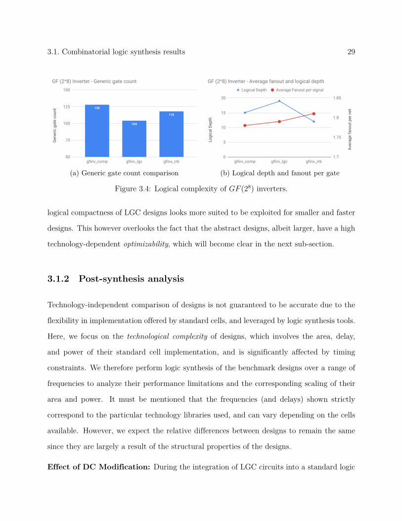
Figure 3.4: Logical complexity of GF (28) inverters.
logical compactness of LGC designs looks more suited to be exploited for smaller and faster
designs. This however overlooks the fact that the abstract designs, albeit larger, have a high
technology-dependent optimizability, which will become clear in the next sub-section.
3.1.2 Post-synthesis analysis
Technology-independent comparison of designs is not guaranteed to be accurate due to the
flexibility in implementation offered by standard cells, and leveraged by logic synthesis tools.
Here, we focus on the technological complexity of designs, which involves the area, delay,
and power of their standard cell implementation, and is significantly affected by timing
constraints. We therefore perform logic synthesis of the benchmark designs over a range of
frequencies to analyze their performance limitations and the corresponding scaling of their
area and power. It must be mentioned that the frequencies (and delays) shown strictly
correspond to the particular technology libraries used, and can vary depending on the cells
available. However, we expect the relative differences between designs to remain the same
since they are largely a result of the structural properties of the designs.
Effect of DC Modification: During the integration of LGC circuits into a standard logic
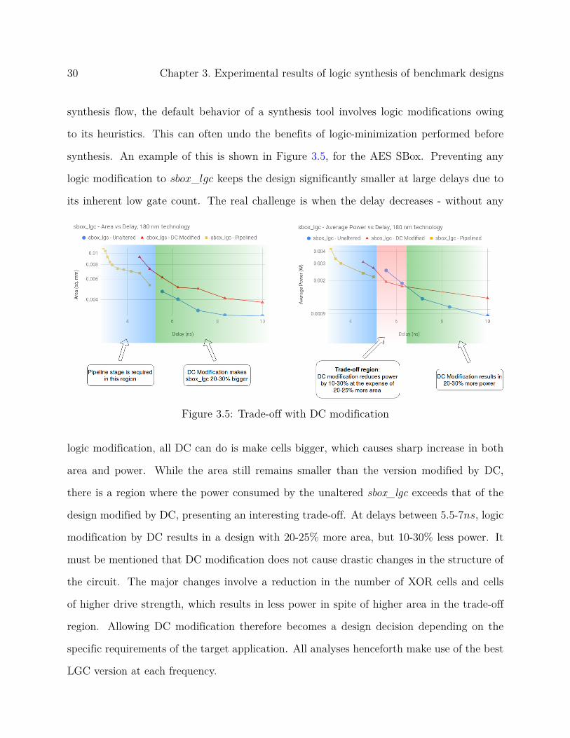
30 Chapter 3. Experimental results of logic synthesis of benchmark designs
synthesis flow, the default behavior of a synthesis tool involves logic modifications owing
to its heuristics. This can often undo the benefits of logic-minimization performed before
synthesis. An example of this is shown in Figure 3.5, for the AES SBox. Preventing any
logic modification to sbox_lgc keeps the design significantly smaller at large delays due to
its inherent low gate count. The real challenge is when the delay decreases - without any
Figure 3.5: Trade-off with DC modification
logic modification, all DC can do is make cells bigger, which causes sharp increase in both
area and power. While the area still remains smaller than the version modified by DC,
there is a region where the power consumed by the unaltered sbox_lgc exceeds that of the
design modified by DC, presenting an interesting trade-off. At delays between 5.5-7ns, logic
modification by DC results in a design with 20-25% more area, but 10-30% less power. It
must be mentioned that DC modification does not cause drastic changes in the structure of
the circuit. The major changes involve a reduction in the number of XOR cells and cells
of higher drive strength, which results in less power in spite of higher area in the trade-off
region. Allowing DC modification therefore becomes a design decision depending on the
specific requirements of the target application. All analyses henceforth make use of the best
LGC version at each frequency.

3.1. Combinatorial logic synthesis results 31
3.1.2.1 AES SBox
The important results of our analysis are selected and listed for detailed discussion as follows.
1. sbox_lgc is the smallest of all in the minimal-area region. Figure 3.6 shows
the plot of area versus delay for the SBox at the 180nm and 32nm technology nodes.
The compactness of sbox_lgc can be clearly seen in the minimal-area region, where it is
17-55% smaller than sbox_lut, and 5-25% smaller than sbox_canright.
(a) TSMC 180nm standard cell library (b) Synopsys SAED 32nm standard cell library
Figure 3.6: Area vs Delay for SBox designs - technology-specific comparison.
2. sbox_lgc is well-suited for pipelining at the high-speed region. The effect of
timing constraints is seen around 200-240 MHz (4-5ns delay), through a sharp increase
in the area of sbox_lgc, sbox_wolkerstorfer, and sbox_canright; in the 180nm node, they
actually exceed that of sbox_lut. This is expected when the design transitions from its
minimal-area region to the high-speed region where logic modification and an increase in
cell count and drive strengths are needed to meet timing.
The compactness of sbox_lgc can be exploited in this region to add a pipeline stage, after
which its area gain over sbox_lut stays within ±20%. Increased branching in sbox_lut
results in the retiming heuristics inserting more registers into the logic cloud, causing a

32 Chapter 3. Experimental results of logic synthesis of benchmark designs
greater increase in area. On the other hand, the small fanout of logic-minimized designs
keeps the area-increase after retiming to a level that is of practical utility. Among the
logic-minimized designs, sbox_lgc reaches a smaller delay (2.6 ns) compared to sbox_canright
(2.9 ns), but sbox_canright stays between 4-20% smaller than sbox_lgc after pipelining.
3. Without pipelining, sbox_lut achieves a better area-delay trade-off. Figure 3.7
gives an insight of the nature of optimization performed on the SBox designs. sbox_lut
has the highest average post-synthesis fanout and the least depth among all non-pipelined
designs. Despite high logical depth before synthesis, optimization during synthesis greatly
reduces the number of logic levels, along with a small increase in fanout. Similar to its
area, the fanout of sbox_lut remains flat as the frequency increases, indicating greater
flexibility to technology-dependent optimization.
On the contrary, the synthesis process increases the fanout and depth of logic-minimized
designs. Inserting a pipeline stage reduces the logical depth of sbox_lgc, which makes it
feasible to increase the fanout of each individual gate while still meeting timing. Without
pipelining, there is little or no scope for reducing logic levels, which necessitates increased
drive strength and addition of logic to meet timing at high speeds. Furthermore, logic-
minimized designs are highly XOR-dominant, as opposed to sbox_lut. Increasing the
drive strength of large number of XOR gates becomes expensive due to their higher area
as compared to other cells in the library (as was initially shown in Figure 1.4). sbox_lut,
in contrast, consists of zero XOR gates both before and after synthesis. This eventually
ends up having a greater impact on the area of logic-minimized designs. The number of
XOR cells after synthesis was observed to have an increased correlation to the design’s
area as we move into the high-speed region, and the plot can be found in Appendix A.
4. sbox_lut is more power-efficient in the 180nm technology node. This counter-
intuitive result suggests that area efficiency of sbox_lgc does not necessarily imply its
3.1. Combinatorial logic synthesis results 33
Delay (ns)
Aver
age
fano
ut
2
2 4 6 8 10
sbox_lut
sbox_wolkerstorfer
sbox_lgc
sbox_canright
sbox_pprm1
sbox_pprm3
sbox_wolkerstorfer - Pipelined
sbox_lgc - Pipelined
sbox_canright -
SBox - Average fanout of signal nets vs Delay180nm tecnology
(a) Fanout per gate
Delay (ns)
Num
. log
ic le
vels
10
20
2 4 6 8 10
sbox_lut
sbox_wolkerstorfer
sbox_lgc
sbox_canright
sbox_pprm1
sbox_pprm3
sbox_wolkerstorfer - Pipelined
sbox_lgc - Pipelined
sbox_canright -
SBox - Circuit depth vs Delay - 180nm technology
(b) Maximum number of logic levels
Figure 3.7: Greater branching and fewer logic levels in sbox_lut.
power efficiency. In the minimal-area region where sbox_lgc was 25-55% smaller than
sbox_lut, the former’s power benefit decreases from 21% to -8%, and continues decreasing
in the high-speed region.
Delay (ns)
Aver
age
Pow
er (W
)
0.001
0.002
0.004
0.006
0.008
4 6 8 10
sbox_lut
sbox_wolkerstorfer
sbox_lgc
sbox_canright
sbox_pprm1
sbox_pprm3
sbox_wolkerstorfer - Pipelined
sbox_lgc - Pipelined
sbox_canright - Pipelined
SBox - Average power vs Delay - 180 nm technology
(a) TSMC 180 nm standard cell library.
Delay (ns)
Aver
age
Pow
er (W
)
0.00004
0.00006
0.00008
0.0001
4 6 8 10
sbox_lut
sbox_wolkerstorfer
sbox_lgc
sbox_canright
sbox_pprm3
sbox_wolkerstorfer - Pipelined
sbox_lgc - Pipelined
sbox_canright - Pipelined
SBox - Average Power vs Delay - 32 nm technology
(b) SAED 32/28 nm standard cell library.
Figure 3.8: Average power consumption of SBox designs plotted against delay.
There are two major reasons for this. First, as discussed in the area analysis, reducing the
delay of sbox_lgc involves increasing the size and drive strengths of the cells. This causes
higher power consumption during every switching activity. For reference, in the TSMC
180nm technology used, dynamic power consumption of 2-input XOR and AND gates
with drive strength X2 and X4 can be anywhere between 1.6-2× and 2.8-3.9× greater

34 Chapter 3. Experimental results of logic synthesis of benchmark designs
than that of their X1 counterparts. At a delay of 4.5 ns, sbox_lut has 8× more X1
cells, whereas sbox_lgc consists of 2.5× more X4 and 2× more X8 cells (Figure 3.9(a)),
explaining both the higher area and power at that speed.
Drive Strength
Num
ber o
f cel
ls
1
510
50100
X1 X2 X3 X4 X8 X12 X20
sbox_lut sbox_lgc sbox_wolkerstorfer sbox_canright
SBox - Distribution of standard cell drive strengths in high-speed region
(a) Cell drive strength distribution (4.5 ns delay)
Delay (ns)
Num
. tog
gles
per
com
puta
tion
200
300
4 6 8 10
sbox_lut
sbox_wolkerstorfer
sbox_lgc
sbox_canright
sbox_comp - Pipelined
sbox_lgc - Pipelined
sbox_canright - Pipelined
SBox - Toggles per computation
(b) Toggle count per SBox computation.
Figure 3.9: Drive strength and toggling of cells influence dynamic power.
The second reason is that greater toggling directly results in higher dynamic power,
which contributes to more than 99% of total power consumption at this technology node.
Although sbox_lut is 30-40% bigger with 2.5× more cells in the minimal-area region, it
involves just 5-10% more toggles per computation than sbox_lgc (Figure 3.9(b)). This
is reflective of the fact that by virtue of its ROM-structure, sbox_lut does consist of
more cells but very few of them are active for a particular table look-up, whereas logic-
minimized designs have a greater fraction of their cells active for each operation. The
higher toggling of logic-minimized designs is because they are dominated by dynamic
hazard-transparent XOR gates [36]. An XOR gate propagates a transition on any of its
inputs with a probability of 1, as opposed to a probability of 0.5 in other gates. The high
correlation of XOR count to the designs’ power consumption is shown in Appendix A.
Since sbox_lut is completely mapped and optimized by DC, XOR gates do not make up
a majority of the design. In summary, sbox_lgc toggles almost as much as sbox_lut, but
each toggle of the former is more expensive.
3.1. Combinatorial logic synthesis results 35
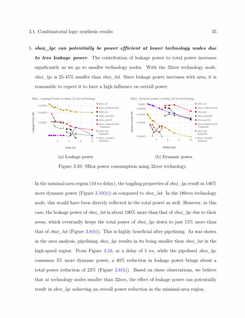
5. sbox_lgc can potentially be power efficient at lower technology nodes due
to less leakage power. The contribution of leakage power to total power increases
significantly as we go to smaller technology nodes. With the 32nm technology node,
sbox_lgc is 25-45% smaller than sbox_lut. Since leakage power increases with area, it is
reasonable to expect it to have a high influence on overall power.
Delay (ns)
Leak
age
Pow
er (W
)
0.00002
0.00003
0.00004
4 6 8 10
sbox_lut
sbox_wolkerstorfer
sbox_lgc
sbox_canright
sbox_pprm3
sbox_wolkerstorfer - Pipelined
sbox_lgc - Pipelined
sbox_canright - Pipelined
SBox - Leakage Power vs delay, 32 nm technology
(a) Leakage power
Delay (ns)
Dyna
mic
pow
er (W
)
0.00002
0.00004
0.00006
0.00008
0.0001
4 6 8 10
sbox_lut
sbox_wolkerstorfer
sbox_lgc
sbox_canright
sbox_pprm3
sbox_wolkerstorfer - Pipelined
sbox_lgc - Pipelined
sbox_canright - Pipelined
SBox - Dynamic power vs Delay, 32 nm technology
(b) Dynamic power.
Figure 3.10: SBox power consumption using 32nm technology.
In the minimal-area region (10 ns delay), the toggling properties of sbox_lgc result in 146%
more dynamic power (Figure 3.10(b)) as compared to sbox_lut. In the 180nm technology
node, this would have been directly reflected in the total power as well. However, in this
case, the leakage power of sbox_lut is about 190% more than that of sbox_lgc due to their
areas, which eventually keeps the total power of sbox_lgc down to just 15% more than
that of sbox_lut (Figure 3.8(b)). This is highly beneficial after pipelining. As was shown
in the area analysis, pipelining sbox_lgc results in its being smaller than sbox_lut in the
high-speed region. From Figure 3.10, at a delay of 5 ns, while the pipelined sbox_lgc
consumes 3% more dynamic power, a 40% reduction in leakage power brings about a
total power reduction of 23% (Figure 3.8(b)). Based on these observations, we believe
that at technology nodes smaller than 32nm, the effect of leakage power can potentially
result in sbox_lgc achieving an overall power reduction in the minimal-area region.

36 Chapter 3. Experimental results of logic synthesis of benchmark designs
Summary: We conclude this analysis with Table 3.1, where of sbox_lgc is compared with
the two best benchmark designs. In the table, - indicates smaller area (or lower power),
while + indicates higher area/power of sbox_lgc over its alternatives. The compactness of
sbox_lgc is well-reflected in hardware at low speeds. Achieving higher speeds comes at the
cost of an increase in both area and power over an abstract LUT-based design.
Benchmark Design Region Area PowerComparison of sbox_lgc Min-Area - 54% - 11-20%
with sbox_lut High-Speed + 2-13% +12-40%Comparison of sbox_lgc Min-Area - 17-24% - 4-36%
with sbox_canright High-Speed + 4-22% + 3-23%
Table 3.1: Summary of analysis results for sbox_lgc with TSMC 180 nm technology library.
3.1.2.2 Binary Polynomial multiplication
The analysis of polynmial multipliers is performed for multiplier sizes ranging from 8 to 22
bits, and is divided into two sets - (i) Varying the multiplier size (N) at fixed delays, and (ii)
Varying the delay for each value of N . The reason is that the space complexity of polynomial
multiplication grows quadratically with N , and hence, an architecture that scales better with
N is desired. It can be noted from Figure 3.11(a) that the area-delay curve follows a similar
pattern for different multiplier sizes.
Salient results of this analysis are listed as follows.
1. A matrix-based polynomial multiplier scales better with N at higher speeds.
Figure 3.11(a) shows that minimal-area designs of polymult_lgc and polymult_comp are
smaller than polymult_mat. This is understandable because the former two are inherently
compact, and a minimal area design doesn’t involve significant modification by DC since
the designs meet timing comfortably. Moreover, this area reduction increases with N .

3.1. Combinatorial logic synthesis results 37
(a) Area vs Delay for fixed sizes (b) Area vs N at fixed delays.
Figure 3.11: Area comparison for polynomial multipliers using TSMC 180nm technology.
For instance, polymult_lgc is only 6% smaller than polymult_mat in the minimal-area
region for an 8× 8 multiplier, whereas it is 25% smaller in the same region for a 22× 22
multiplier. This trend is shown in Figure 3.13(a).
As the delay decreases, polymult_lgc and polymult_comp incur a sharp increase in area to
a point where their plots cross that of polymult_mat, beyond which they are constantly
greater than polymult_mat. This rate of increase and the difference in the areas of
polymult_lgc and polymult_mat increases with N . polymult_lgc is 25% bigger than poly-
mult_mat for an 8× 8 multiplier, while it gets upto 40-50% bigger for larger multipliers.
This can also be intuitively understood from Figure 3.11(b), where the gap between the
areas of polymult_lgc and polymult_mat widens with the delay for each value of N . Note:
In Figure 3.11(b), the area of polymult_mat remains unchanged for both 10ns and 3ns
delay, while polymult_lgc gets bigger.
These observations are a result of the balanced tree structure of polymult_mat (Figure
3.12(a)), which offers remarkable potential to collapse the circuit into fewer levels of gates.
The logical depth of polymult_lgc on the other hand, really depends on the sub-expressions
factored out and the logic minimization heuristics at work. This is also seen in Figure
3.12(b) where polymult_mat is synthesized with significantly fewer levels (within 6-10)
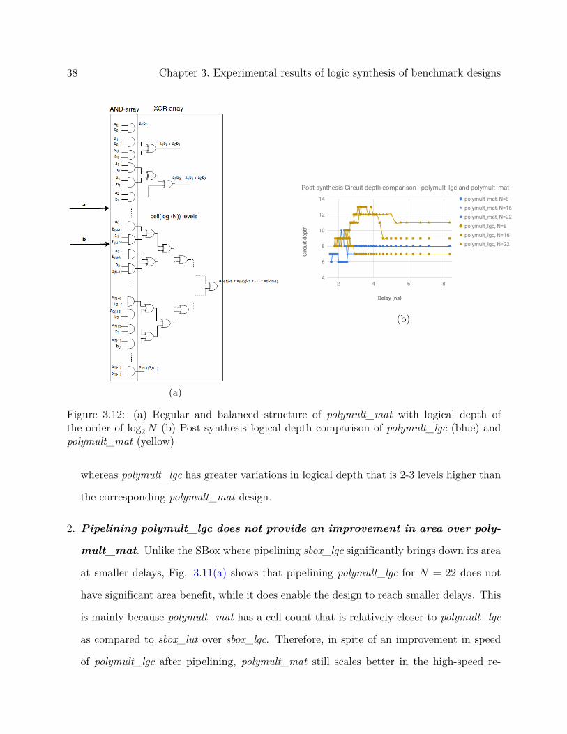
38 Chapter 3. Experimental results of logic synthesis of benchmark designs
(a)
Delay (ns)Ci
rcui
t dep
th
4
6
8
10
12
14
2 4 6 8
polymult_mat, N=8
polymult_mat, N=16
polymult_mat, N=22
polymult_lgc, N=8
polymult_lgc, N=16
polymult_lgc, N=22
Post-synthesis Circuit depth comparison - polymult_lgc and polymult_mat
(b)
Figure 3.12: (a) Regular and balanced structure of polymult_mat with logical depth ofthe order of log2N (b) Post-synthesis logical depth comparison of polymult_lgc (blue) andpolymult_mat (yellow)
whereas polymult_lgc has greater variations in logical depth that is 2-3 levels higher than
the corresponding polymult_mat design.
2. Pipelining polymult_lgc does not provide an improvement in area over poly-
mult_mat. Unlike the SBox where pipelining sbox_lgc significantly brings down its area
at smaller delays, Fig. 3.11(a) shows that pipelining polymult_lgc for N = 22 does not
have significant area benefit, while it does enable the design to reach smaller delays. This
is mainly because polymult_mat has a cell count that is relatively closer to polymult_lgc
as compared to sbox_lut over sbox_lgc. Therefore, in spite of an improvement in speed
of polymult_lgc after pipelining, polymult_mat still scales better in the high-speed re-

3.1. Combinatorial logic synthesis results 39
gion. Figure 3.11(b) shows the area after pipelining polymult_lgc and polymult_comp for
different sizes at a delay of 2.2ns. The area is consistently higher than polymult_mat,
indicating that pipelining logic-minimized multipliers does not offer a better area-delay
trade-off over a non-pipelined matrix multiplier.
3. The differences in area between polymult_lgc and polymult_comp are within
±20%, with polymult_comp marginally better at high speeds. Figure 3.13(b)
shows the percentage of area reduction obtained from polymult_lgc over polymult_comp.
Delay (ns)
Perc
enta
ge o
f are
a re
duct
ion
-75%
-50%
-25%
0%
25%
50%
2 3 4 5 6
N=8 N=12 N=16 N=20 N=22
Percentage reduction in area of polymult_lgc over polymult_mat, 180nm
(a) Reduction over polymult_mat
Delay (ns)
Perc
enta
ge o
f are
a re
duct
ion
-30%
-20%
-10%
0%
10%
20%
2 3 4 5 6
N=8 N=11 N=16 N=17 N=22
Percentage reduction in area of polymult_lgc over polymult_comp - 180nm
(b) Reduction over polymult_comp
Figure 3.13: Reduction in area of polymult_lgc over alternatives.
The differences between polymult_lgc and polymult_comp are largely within 15% at the
minimal-area region. Figure 3.13(b) suggests no clear pattern either with respect to N
or with respect to delay. For instance, polymult_lgc has a clear positive area reduction
percentage for N = 11 and N = 22, whereas, for N = 16 and N = 17, there are
opposing patterns of area reduction at the minimal-area and high-speed regions. We
believe that these variations are due to the fact that the logic minimization techniques
used in polymult_lgc and polymult_comp are very similar, with the former incorporating
additional techniques over many of the latter’s designs. As a result, the differences in their
logical descriptions are minimal, and the variations in post-synthesis area largely stem
from specific standard cells used and the individual circuit structures after optimization.

40 Chapter 3. Experimental results of logic synthesis of benchmark designs
4. The power consumed by a matrix-based multiplier scales better with both N
and delay. This point can be observed from Figures 3.14(a) and 3.14(b), for 180nm
technology. Similar figures for 32nm technology are presented in Appendix A. The dif-
ferences in power consumption for small values of N are negligible, but become higher as
N increases to 22. In the minimal-area region, the power benefit offered by polymult_lgc
depends on the size. There is upto a 15% power reduction for most values of N < 15,
but beyond that, there is an increase in power consumed by polymult_lgc. As speed in-
creases, the benefits in power decrease as well, and in the high-speed region, there is up
to a 70-80% increase in power for certain values of N .
Delay (ns)
Ave
rage
Pow
er (W
)
0
0.0025
0.005
0.0075
0.01
2 4 6 8 10
polymult_mat, N=8
polymult_lgc, N=8
polymult_mat, N=12
polymult_lgc, N=12
polymult_mat, N=16
polymult_lgc, N=16
polymult_mat, N=22
polymult_lgc, N=22
Power vs Delay for NXN polynomial multipliers - 180nm technology
(a)
N
Aver
age
Pow
er (W
)
0
0.0025
0.005
0.0075
0.01
8 10 12 14 16 18 20 22
polymult_mat, 10 ns
polymult_lgc, 10 ns
polymult_mat, 4 ns
polymult_lgc, 4 ns
polymult_mat, 2.9 ns
polymult_lgc, 2.9 ns
Power vs N - 180 nm technology
(b)
Figure 3.14: Average power of polynomial multipliers using TSMC 180nm technology.
5. Dynamic Power is significantly influenced by gates with unbalanced input
delays. In case of the SBox, it was argued that the inherent structure of an LUT-based
design results in fewer cells being active at any instant that makes its power scale bet-
ter at high speeds. Here, polymult_mat is a bit-parallel design where such a property
is not expected to exist. Moreover, both the designs are dominated by similar types of
gates, which means it is reasonable to expect sbox_lgc to consume lesser power in the
minimal-area region. However, polymult_mat still consumes less power in the minimal-
area region than polymult_lgc due to fewer toggles per computation. This, we found, is a

3.1. Combinatorial logic synthesis results 41
Delay (ns)
Num
ber o
f XO
R ce
lls
0
100
200
300
400
2 4 6 8 10
polymult_mat, N=8
polymult_lgc, N=8
polymult_mat, N=16
polymult_lgc, N=16
polymult_mat, N=20
polymult_lgc, N=20
polymult_mat, N=22
polymult_lgc, N=22
Number of XOR cells with unbalanced input delays
(a) Comparison for XOR cells
Delay (ns)
Num
ber o
f gat
es
0
200
400
600
2 4 6 8 10
polymult_mat, N=8
polymult_lgc, N=8
polymult_mat, N=16
polymult_lgc, N=16
polymult_mat, N=20
polymult_lgc, N=20
polymult_mat, N=22
polymult_lgc, N=22
Total number of cells with unbalanced input delays
(b) Comparison for all cells
Figure 3.15: Cells with unbalanced input levels, using 180 nm technology node.
result of gates having unbalanced delays at their inputs. This point has been previously
mentioned with regards to the construction of an SBox [36]. In spite of both designs
being XOR-dominant, polymult_lgc has more gates which have their inputs at different
logic levels (Figure 3.15). This can again be traced back to the inherent balanced struc-
ture of polymult_mat (Figure 3.12(a)). While LGC tools [8, 12] make use of gate count
and/or logical depth as their cost function, the process can potentially increase power
consumption by removing certain properties of the design such as balanced logic levels.
Summary: Figure 3.16 presents a heat map depicting the high area-efficiency of LGC
designs at low speeds for all sizes, and their power-efficiency at low speeds only for small
multipliers. A matrix-based multiplier is a better choice at high speeds with regard to both
area and power-efficiency.
3.1.2.3 Galois Field Multiplication
1. The TOF-based LGC designs are smaller. The area estimate from technology-
independent analysis in this case was fairly accurate, considering the observation that gf-
mult_lgc and gfmult_lgc_tof are around 25% and and 15% smaller than gfmult_mastrovito

42 Chapter 3. Experimental results of logic synthesis of benchmark designs
(a) Area-efficiency over polymult_mat (b) Power-efficiency over polymult_mat
Figure 3.16: Heat map illustrating the area and power-efficiency of polymult_lgc.
and gfmult_paar respectively in the minimal-area region for GF (28) multiplication. For
GF (216) multiplication, gfmult_lgc_tof is the most compact at low speeds, and is 25%
and 20% smaller than gfmult_mastrovito and gfmult_paar respectively.
GF(28) GF(216)
(a) TSMC 180nm standard cell library
GF(28)GF(216)
(b) SAED 32/28nm standard cell library
Figure 3.17: Area-delay plot for GF multiplier designs.
The representations of gfmult_paar and gfmult_mastrovito are matrix-based, which makes
them more optimzeable. Still, this does not degrade the area benefit of LGC designs for
GF (28) multiplication. At the high-speed region, gfmult_lgc and gfmult_lgc_tof are 20%
smaller than gfmult_mastrovito, and 10% smaller than gfmult_paar. There is however,

3.1. Combinatorial logic synthesis results 43
an impact on the area of gfmult_lgc_tof in GF (216) multiplication, where it offers an
area benefit within ±5% of gfmult_mastrovito and gfmult_paar. The extremely compact
logical structure of gfmult_lgc_tof makes it possible for it to not significantly exceed the
areas of the other two designs in spite of logic addition during synthesis. The cell counts of
gfmult_mastrovito and gfmult_paar about 20-30% greater than gfmult_lgc_tof, but that
is offset by the higher drive strength (and hence bigger size) of those of the latter, and
the small differences in area really come down to specific technology mapping operations
performed by DC.
2. Including the mapping and inverse mapping operations over the LGC de-
signs is expensive. In case of GF (216) multiplication, in contrast to the small size of
gfmult_lgc_tof, we see that adding the mapping operations makes the area of gfmult_lgc
more than double that of the other designs. We therefore believe that using gfmult_lgc_tof
offers compactness for designs where the mapping operations are either merged with other
linear transformations, or where they are performed once at the very beginning and the
end of a series of operations including GF multiplication in TOF representation. In case a
logic-minimized GF multiplier for a particular field polynomial is desired, using an LGC
design specific to that polynomial can give a compact design, as is seen from the area
plots for GF (28) multiplication for the AES polynomial. Another alternative is that the
GF multiplier in TOF-representation can be optimized by LGC designs together with the
mapping operations. We however did not have such an SLP, and hence cannot comment
on the area properties of the same.
3. The TOF-based LGC GF multipliers are more power-efficient. For GF (28)
multiplication, gfmult_lgc_tof consumes 30-35% less power than both gfmult_paar and
gfmult_mastrovito. In addition to the extreme compactness of the LGC design, the
low complexity of a GF (28) multiplier means very few logic levels (7-8) as compared to

44 Chapter 3. Experimental results of logic synthesis of benchmark designs
gfmult_paar (9-10). The area of gfmult_lgc_tof does not blow up due to bigger cells,
and the power therefore remains very low.
Delay (ns)
Aver
age
Pow
er (W
)
0.0005
0.001
0.005
0.01
2 4 6 8 10
gfmult_mastrovito, 2^8
gfmult_paar, 2^8
gfmult_lgc, 2^8
gfmult_lgc_tof, 2^8
gfmult_mastrovito, 2^16
gfmult_paar, 2^16
gfmult_lgc, 2^16
gfmult_lgc_tof, 2^16
Power vs Delay for GF Multipliers - 180 nm technology
(a) TSMC 180nm technology
Delay (ns)
Aver
age
Pow
er (W
)
0
0.0001
0.0002
0.0003
2 4 6 8 10
gfmult_mastrovito, 2^8
gfmult_paar, 2^8
gfmult_lgc, 2^8
gfmult_lgc_tof, 2^8
gfmult_mastrovito, 2^16
gfmult_paar, 2^16
gfmult_lgc_tof, 2^16
Power vs Delay for GF Multipliers - 32 nm technology
(b) Synopsys 32nm technology
Figure 3.18: (a) Average power consumption of GF multipliers plotted against delay
In case of GF (216) multiplication, when mapping and inverse mapping are applied exter-
nally, gfmult_lgc consumes 2× higher power as compared to the matrix-based designs.
Without mapping, gfmult_lgc_tof has 11-12 logic levels as compared to gfmult_paar’s
12, which is due to the balanced properties of the latter, making it scale better with speed.
In spite of having 150-200 fewer cells, the power of gfmult_lgc_tof remains within ±10%
of gfmult_paar due to higher toggles and bigger cells.
Summary: LGC GF multipliers based on Tower-of-Fields representation are compact and
power-efficient at most frequencies. At high speeds, their power consumption is not substan-
tially higher than that of benchmark designs. Conversion to and from a standard representa-
tion using mapping operations around the LGC multiplier results in large and power-hungry
hardware. Table 3.2 summarizes the comparison of LGC designs with gfmult_paar.

3.1. Combinatorial logic synthesis results 45
Comparison with gfmult_paarMinimal-area region High-speed regionLGC Design
Area Power Area PowerGF (28) Multiplier
TOF-based - 12-25% - 29-40 ±15% ± 15%
GF (28) MultiplierAES Polynomial - 12-25% - 21-31% - 1-15% - 6-15%
GF (216) MultiplierTOF-based - 15-19% - 2-4% ± 8% ± 10%
GF (216) MultiplierTOF, External mapping + 36-170% + 200% + 200% + 200%
Table 3.2: Summary of analysis results for gfmult_lgc with TSMC 180 nm technology library.
3.1.2.4 Galois Field Inversion
gfinv_lgc is smaller than gfinv_comp but larger than gfinv_rrb. In most cases,
gfinv_rrb is significantly smaller than gfinv_lgc. The starting design of gfinv_lgc has a
logical depth of 19 to gfinv_rrb’s 12, while of having only 12 fewer gates. In addition,
gfinv_rrb has a greater parallelism in its structure, indicated by its high fanout (Figure
3.4(b)). All of these are reflected in the post-synthesis results. Due to significantly fewer
logic levels, the area of gfinv_rrb scales better with delay, and attains a minimum delay of
2.9 ns as compared to 3.8 ns by gfinv_lgc. Higher parallelism and lower logical depth also
enable a smoother transition into the high-speed region. This is because gfinv_lgc incurs a
sharp increase in cell count to meet timing, in contrast to the relatively flat cell count plot
of gfinv_rrb (Figure 3.20(a)).
Pipelining gfinv_lgc does have an observable reduction in area at a delay of 3.8-4.1 ns with
the 180 nm technology node, and enables the design to reach delays as low as those of
gfinv_rrb. While gfinv_lgc is up to 107% larger than gfinv_rrb in the high-speed region
without pipelining, it is brought down to sizes that are 35-55% larger than gfinv_rrb by
inserting a pipeline stage. This is due to reduction in logical depth (Figure 3.20(b)), which

46 Chapter 3. Experimental results of logic synthesis of benchmark designs
Delay (ns)
Area
(KG
E)
0
0.25
0.5
0.75
1
4 6 8 10
gfinv_comp
gfinv_lgc
gfinv_rrb
gfinv_lgc - pipelined
gfinv_comp - pipelined
GF(2^8) Inverter - Area (K Gate Eq.) vs Delay, 180 nm technology
(a)
Delay (ns)
Area
(KG
E)
0
0.1
0.2
0.3
4 6 8 10
gfinv_comp
gfinv_lgc
gfinv_rrb
gfinv_comp - pipelined
gfinv_lgc - pipelined
GF(2^8) Inverter - Area(K Gate Eq.) vs Delay, 32 nm technology
(b)
Figure 3.19: Area-delay plot for GF (28) inverter designs using (a) TSMC 180nm, and b)SAED 32/28nm standard cell libraries.
is however offset by the large cell count to make the overall area bigger.
Delay (ns)
Cell
coun
t
50
100
150
200
250
4 6 8 10
gfinv_comp
gfinv_lgc
gfinv_rrb
gfinv_lgc - pipelined
GF (2^8) Inverter - Cell count vs Delay, 180 nm technology
(a)
Delay (ns)
Circ
uit D
epth
0
5
10
15
20
25
4 6 8 10
gfinv_comp
gfinv_lgc
gfinv_rrb
gfinv_lgc - pipelined
GF (2^8) Inverter - Circuit depth vs Delay, 180 nm technology
(b)
Figure 3.20: Post-synthesis Cell count and logical depth of for GF (28) inverter designs using180 nm technology.
Power comparison of GF inverter designs (Figure 3.21) shows similar patterns observed
during area analysis, that are a direct result of the better parallelism gfinv_rrb.

3.2. Integrated Design Examples 47
Delay (ns)
Aver
age
pow
er (W
)
0
0.0005
0.001
0.0015
0.002
0.0025
4 6 8 10
gfinv_comp gfinv_lgc gfinv_rrb
GF(2^8) Inverter - Power vs Delay, 180 nm technology
(a) TSMC 180nm technology
Delay (ns)
Aver
age
Pow
er (W
)
0
0.000025
0.00005
0.000075
0.0001
4 6 8 10
gfinv_comp gfinv_lgc gfinv_rrb
GF(2^8) Inverter - Power vs Delay, 32 nm technology
(b) Synopsys SAED 32nm technology
Figure 3.21: (a) Average power consumption of GF (28) inverters plotted against delay
3.2 Integrated Design Examples
The analyses performed in Section 3.1.2 were entirely based on the consideration of com-
binatorial blocks as standalone primitives. The primary reason for having chosen these
benchmarks in Section 2.1 was that they often have practical utility in bigger designs. We
believe that it is important to assess the effectiveness of combinatorial optimization towards
minimizing the area or power of the complete system they are a part of. For instance, it
is not very beneficial to have large area reduction of a combinatorial primitive leading to
negligible (say, less than 5%) reduction in the total system area. This is affected by both
the contribution of the primitive to the bigger design’s area, as well as the optimization
performed by combining these primitives with external logic that is part of the design. This
section analyzes two such designs - AES encryption engine and Reed-Solomon encoder.
3.2.1 Comparison of AES designs with different SBox circuits
In this sub-section, we analyze the logic synthesis results of AES designs making use of
different SBox circuits. The aim of this study is to highlight the diversity in AES designs,

48 Chapter 3. Experimental results of logic synthesis of benchmark designs
and the fact that evaluating logic-minimized combinatorial primitives highly depends on the
type of design they are plugged into. It was of interest to observe if the area or power results
varied with varying number of SBox structures. Similar results for 32 nm technology can be
found in Appendix A.
Figure 3.22: Standard and high-throughput AES designs.
3.2.1.1 Standard AES
This is an AES design with one SBox per each byte of the state and the key. There are
therefore 20 SBox circuits in total, and each encryption operation is completed in 10 clock
cycles, i.e. one round per clock cycle. The AES design is synthesized with different SBox
designs, with and without pipelining for logic-minimized designs.
The choice of SBox in standard AES is critical because it makes up more than 45% of the
total design. Similar to the standalone SBox results, aes20_lgc is 7% and 32% smaller than
aes20_canright and aes20_lut respectively. Due to better scaling of aes20_lut with speed,
the area reduction of aes20_lgc comes down to about 3% as it enters the high-speed region,
beyond which pipelining keeps the area benefit within 9-16% over aes20_lut. An advantage
of pipelining the design is that although each encryption now takes 20 clock cycles instead of
10, two different encryption operations can be performed in these 20 cycles, thereby ensuring
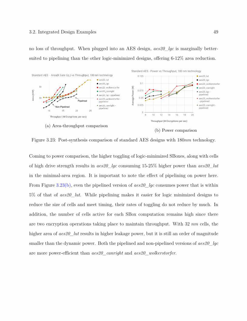
3.2. Integrated Design Examples 49
no loss of throughput. When plugged into an AES design, aes20_lgc is marginally better-
suited to pipelining than the other logic-minimized designs, offering 6-12% area reduction.
Pipelined
Non-Pipelined
(a) Area-throughput comparisonThroughput (M Encryptions per sec)
Aver
age
Pow
er (W
)
0
0.025
0.05
0.075
0.1
0.125
8 10 12 14 16 18 20
aes20_lut
aes20_lgc
aes20_wolkerstorfer
aes20_canright
aes20_lgc - pipelined
aes20_wolkerstorfer - pipelined
aes20_canright - pipelined
Standard AES - Power vs Throughput, 180 nm technology
(b) Power comparison
Figure 3.23: Post-synthesis comparison of standard AES designs with 180nm technology.
Coming to power comparison, the higher toggling of logic-minimized SBoxes, along with cells
of high drive strength results in aes20_lgc consuming 15-25% higher power than aes20_lut
in the minimal-area region. It is important to note the effect of pipelining on power here.
From Figure 3.23(b), even the pipelined version of aes20_lgc consumes power that is within
5% of that of aes20_lut. While pipelining makes it easier for logic minimized designs to
reduce the size of cells and meet timing, their rates of toggling do not reduce by much. In
addition, the number of cells active for each SBox computation remains high since there
are two encryption operations taking place to maintain throughput. With 32 nm cells, the
higher area of aes20_lut results in higher leakage power, but it is still an order of magnitude
smaller than the dynamic power. Both the pipelined and non-pipelined versions of aes20_lgc
are more power-efficient than aes20_canright and aes20_wolkerstorfer.

50 Chapter 3. Experimental results of logic synthesis of benchmark designs
3.2.1.2 High-throughput AES
The second AES design is a high-throughput version. This design employs double the number
of SBox circuits present in standard AES, along with an intermediate set of state registers,
thereby achieving twice the throughput of standard AES. The area and power results are
Throughput (M Encryptions per sec)
Area
(KG
E)
30
40
50
60
20 30 40 50
aes40_lut
aes40_lgc
aes40_wolkerstorfer
aes40_canright
aes40_lgc - pipelined
aes40_wolkerstorfer - pipelined
aes40_canright - pipelined
High-throughput AES - Area (K Gate Eq.) vs Throughput, 180 nm technology
(a)Throughput (M Encryptions per sec)
Aver
age
Pow
er (W
)0
0.05
0.1
0.15
0.2
20 25 30 35 40
aes40_lut
aes40_lgc
aes40_wolkerstorfer
aes40_canright
aes40_lgc - pipelined
aes40_wolkerstorfer - pipelined
aes40_canright - pipelined
High-throughput AES - Power vs Throughput, 180 nm technology
(b)
Figure 3.24: Post-synthesis comparison of high-throughput AES designs.
largely similar to that of the standard AES. The area reduction of aes40_lgc remained about
30% and 15% over aes40_lut and aes40_canright respectively in the minimal-area region.
The increase in number of SBox circuits is reflected in the 32 nm technology node, where the
area gain of aes40_lgc jumps to more than 40% over aes40_lut. The power consumption of
aes40_lgc is higher by 28-40% than that of aes40_lut in the minimal-area region with 180
nm technology. This is more than that seen for standard AES due to doubling of the number
of SBox circuits resulting in higher toggling in them. This difference falls to less than 15%
with 32 nm tehcnology due to the impact of leakage power on the area of aes40_lut.
3.2.1.3 Lightweight AES
The final AES design is a lightweight version (Figure 3.25) consisting of only 4 SBoxes in
total. Multiplexers are inserted at the SBox inputs to send either the round key or one word
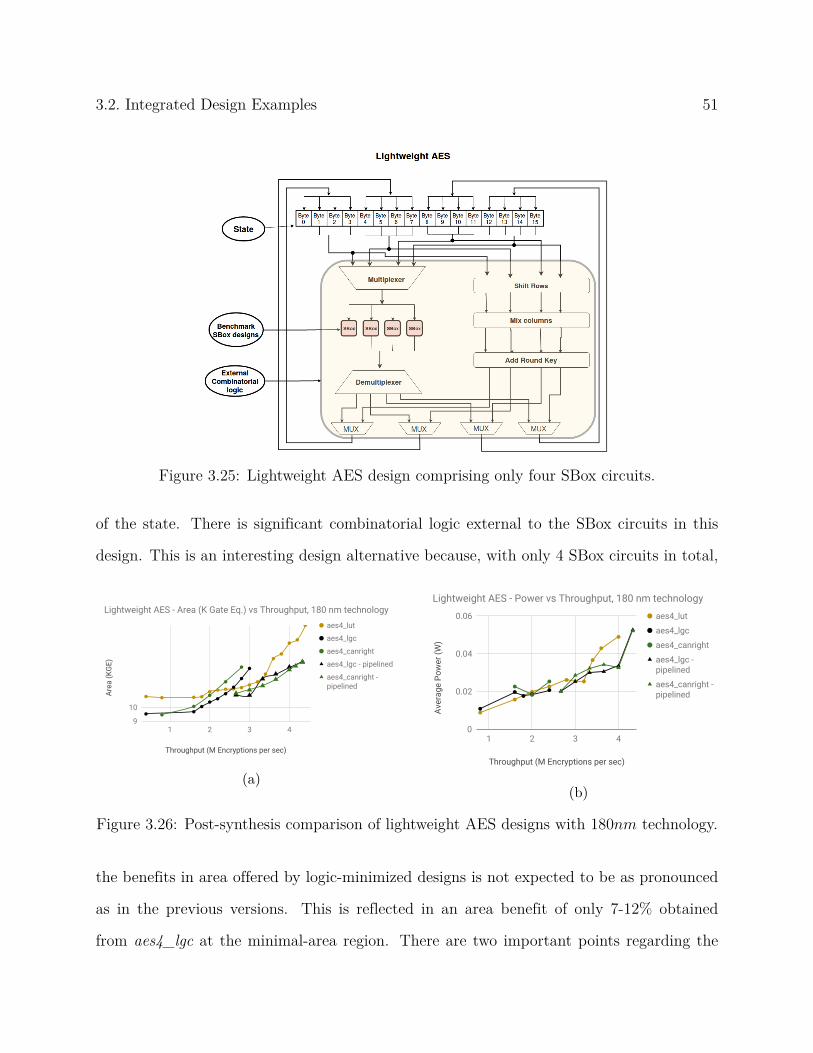
3.2. Integrated Design Examples 51
Figure 3.25: Lightweight AES design comprising only four SBox circuits.
of the state. There is significant combinatorial logic external to the SBox circuits in this
design. This is an interesting design alternative because, with only 4 SBox circuits in total,
Throughput (M Encryptions per sec)
Area
(KG
E)
9
10
1 2 3 4
aes4_lut
aes4_lgc
aes4_canright
aes4_lgc - pipelined
aes4_canright - pipelined
Lightweight AES - Area (K Gate Eq.) vs Throughput, 180 nm technology
(a)Throughput (M Encryptions per sec)
Aver
age
Pow
er (W
)
0
0.02
0.04
0.06
1 2 3 4
aes4_lut
aes4_lgc
aes4_canright
aes4_lgc - pipelined
aes4_canright - pipelined
Lightweight AES - Power vs Throughput, 180 nm technology
(b)
Figure 3.26: Post-synthesis comparison of lightweight AES designs with 180nm technology.
the benefits in area offered by logic-minimized designs is not expected to be as pronounced
as in the previous versions. This is reflected in an area benefit of only 7-12% obtained
from aes4_lgc at the minimal-area region. There are two important points regarding the

52 Chapter 3. Experimental results of logic synthesis of benchmark designs
high-speed region. First, pipelining aes4_lgc comes at a throughput loss of 20%. This is
because this design computes the substitution operation for the AES state in four clock
cycles. There is an additional clock cycle for computing the substitution operation for each
word of the key. After retiming, there is a latency of one cycle per round, and this cycle
cannot be filled by another AES encryption. Second, area of aes4_lut scales sharply in the
high-speed region. This suggests that the external multiplexing logic has a greater impact
on the area of aes4_lut when it comes to meeting timing. Optimization is now performed on
the combined cloud of combinatorial logic, which is seen to be better in the case of aes4_lgc.
This is seen in both the technology nodes, making aes4_lut 10-15% larger than pipelined
versions of logic-minimized designs for similar throughput.
The effect of combined combinatorial optimization is also reflected in the power consumption
of aes4_lut, which goes up to 30% higher than aes4_lgc - pipelined at high speeds. Difficulty
in meeting timing has now resulted in optimization breaking up the structural properties
of aes4_lut with logic addition and modification. This ultimately leads to greater toggling
in aes4_lut than the LGC designs. As for logic-minimized designs, the differences remain
largely within ± 10% after pipelining. With just 4 SBox structures, these differences really
boil down to the specific combined optimization moves performed by the tool.
In summary, the benefits of a smaller SBox are diminished when integrated with an AES
design, especially in its lightweight version. Table 3.3 presents a summary of the analysis of
integration of different SBox circuits with AES designs.
3.2.2 Reed-Solomon Encoder
As mentioned during benchmark selection, we perform logic synthesis with three different
types of logic modification to the LGC combinatorial logic - (i) an exact gate-level represen-

3.2. Integrated Design Examples 53
AES Type Benchmark Design Region Area PowerComparison of aes20_lgc Min-Area - 12-32% + 12-25%
Standard AES with aes20_lut High-Speed - 9-16% - 1-19%(20 SBoxes) Comparison of aes20_lgc Min-Area - 9-14% - 12-21%
with aes20_canright High-Speed - 6-14% (-10%) - (+5%)Comparison of aes4_lgc Min-Area - 3-12% (-8%) - (+25%)
Lightweight AES with aes4_lut High-Speed - 3-16% - 0-30%(4 SBoxes) Comparison of aes4_lgc Min-Area - 4-8% - 0-18%
with aes4_canright High-Speed ± 5% (-11%) - (+3%)
Table 3.3: Analysis summary of AES designs with LGC SBoxes, using 180 nm technology.
tation of the circuit obtained after LGC minimization, referred to as reedsolomon_lgc-exact,
(ii) a design which preserves hierarchy of the LGC-minimized combinatorial logic, allowing
logic modifications only within the combinatorial block, referred to as reedsolomon_lgc-hier,
and (iii) a flattened design that allows DC to merge the LGC-minimized logic blocks with
external logic, referred to as reedsolomon_lgc-flat. As seen from the Figure 2.3, the com-
binatorial logic external to the LGC-minimized block is comparatively minimal to cause a
significant impact on the results. However, it does create different starting solutions by the
tool’s heuristics, which eventually cause observable differences at higher speeds.
3.2.2.1 Area-Throughput comparison
Plugging reedsolomon_lgc as a black-box sans any DC modification is clearly not the best
choice as is indicated by a 17-30% higher area (Figure 3.27(a)). As for reedsolomon_lgc-hier
and redsolomon_lgc-flat, their areas differ by less than 1% in the minimal-area region. This
is due both to negligible external logic and the fact that significant DC optimization kicks
in only when it becomes challenging to meet timing.
Both these designs are about 9-12% larger than reedsolomon_ref in the minimal-area re-
gion. This is a surprising result, considering that reedsolomon_lgc has fewer logic levels and

54 Chapter 3. Experimental results of logic synthesis of benchmark designs
Throughput (million blocks per sec)
Area
(KG
E)
3
4
5
6
7
0.5 0.75 1 1.25 1.5
reedsolomon_lgc - flat
reedsolomon_lgc - exact
reedsolomon_lgc - hier
reedsolomon_ref
RS (255,233) encoder - Area (K Gate Eq.) vs Throughput, 180 nm technology
(a)
Throughput (million blocks per sec)
Area
(KG
E)
1.5
1.75
2
2.25
0.4 0.6 0.8 1 1.2
reedsolomon_lgc - flat
reedsolomon_lgc - hier
reedsolomon_ref
RS (255,233) encoder - Area (K Gate Eq.) vs Throughput, 32 nm technology
(b)
Figure 3.27: Area vs Throughput comparison of Reed Solomon encoder designs
similar cell count, but still ends up bigger than reedsolomon_ref in the minimal-area region.
The reason for this is the higher XOR-dominance of the LGC design. It is true that reed-
solo,on_ref is built using GF multipliers and adders which are predominantly XOR-based,
but their behavioral representation and lack of logic minimization provides greater flexibility
to DC during logic mapping and optimization.
(a) XOR cell count and total standard cell count.
Throughput (million blocks per sec)
Logi
cal D
epth
5
10
15
20
25
0.5 0.75 1 1.25 1.5
reedsolomon_lgc - flat reedsolomon_lgc - exact reedsolomon_lgc - hierreedsolomon_ref
RS (255,223) encoder - Logical Depth, 180 nm technology
(b) Logical depth
Figure 3.28: Post-synthesis comparison of RS(255,223) designs, at 180 nm technology.
Moving on to the high-speed region, the differences between reedsolomon_lgc-flat and reedsolomon_lgc-
hier widen up to 8% due to higher scope for optimization in the latter. On the other hand,
the difference in the areas of reedsolomon_lgc and reedsolomon_ref narrows down to 4-7%.
This is due to the higher circuit depth of reedsolomon_ref that results in sharper increase
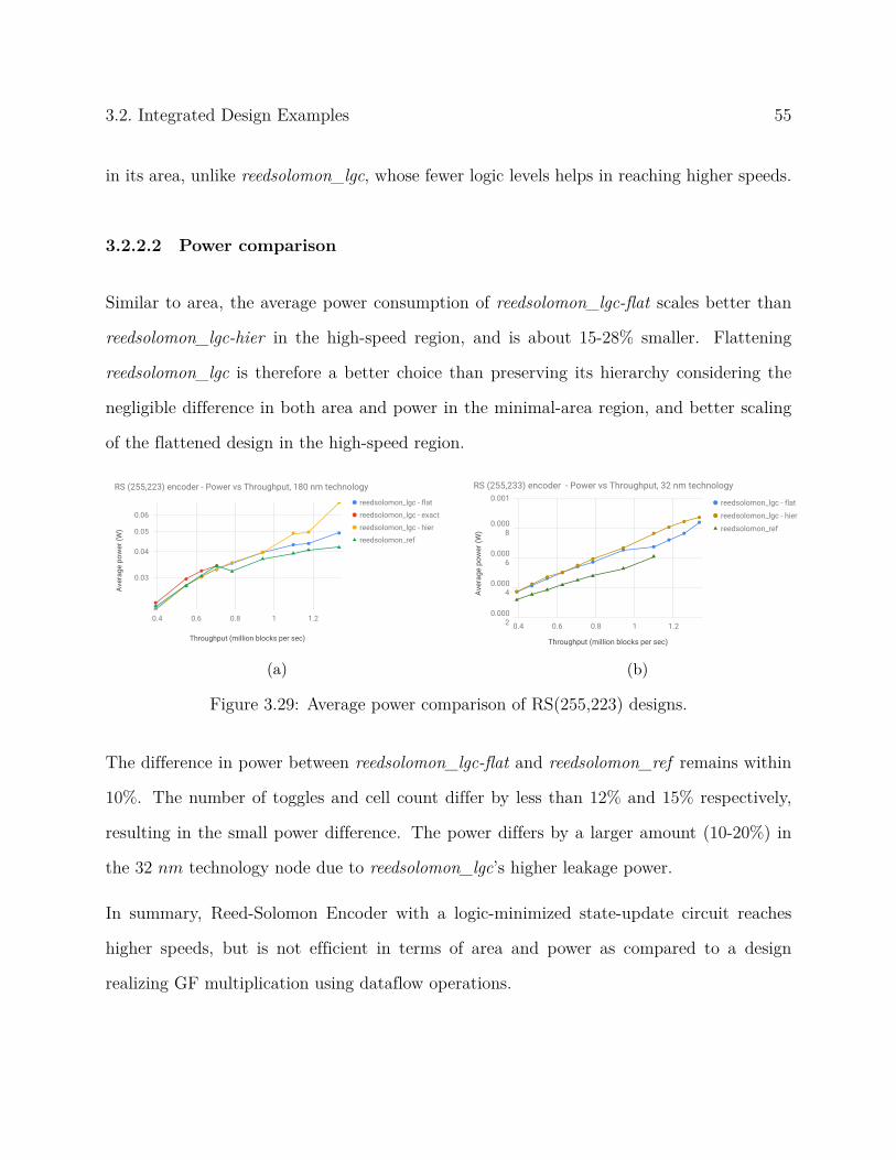
3.2. Integrated Design Examples 55
in its area, unlike reedsolomon_lgc, whose fewer logic levels helps in reaching higher speeds.
3.2.2.2 Power comparison
Similar to area, the average power consumption of reedsolomon_lgc-flat scales better than
reedsolomon_lgc-hier in the high-speed region, and is about 15-28% smaller. Flattening
reedsolomon_lgc is therefore a better choice than preserving its hierarchy considering the
negligible difference in both area and power in the minimal-area region, and better scaling
of the flattened design in the high-speed region.
Throughput (million blocks per sec)
Aver
age
pow
er (W
)
0.03
0.04
0.05
0.06
0.4 0.6 0.8 1 1.2
reedsolomon_lgc - flat
reedsolomon_lgc - exact
reedsolomon_lgc - hier
reedsolomon_ref
RS (255,223) encoder - Power vs Throughput, 180 nm technology
(a)
Throughput (million blocks per sec)
Aver
age
pow
er (W
)
0.0002
0.0004
0.0006
0.0008
0.001
0.4 0.6 0.8 1 1.2
reedsolomon_lgc - flat
reedsolomon_lgc - hier
reedsolomon_ref
RS (255,233) encoder - Power vs Throughput, 32 nm technology
(b)
Figure 3.29: Average power comparison of RS(255,223) designs.
The difference in power between reedsolomon_lgc-flat and reedsolomon_ref remains within
10%. The number of toggles and cell count differ by less than 12% and 15% respectively,
resulting in the small power difference. The power differs by a larger amount (10-20%) in
the 32 nm technology node due to reedsolomon_lgc’s higher leakage power.
In summary, Reed-Solomon Encoder with a logic-minimized state-update circuit reaches
higher speeds, but is not efficient in terms of area and power as compared to a design
realizing GF multiplication using dataflow operations.

56 Chapter 3. Experimental results of logic synthesis of benchmark designs
3.3 Effect of physical design
The final phase of our analysis at multiple abstraction levels is the study of impact of physical
placement and routing on post-synthesis netlists. Area and power after physical design are
liable to change due to physical distances between cells and routing overhead. Therefore,
these results are a more accurate reflection of their behavior on hardware. To analyze these
effects, all the benchmark deigns were placed and routed at multiple frequencies on an
appropriate die size, using Synopsys IC Compiler. It must be mentioned that this physical
design flow was performed only for studying the impact of placement and routing, and not
for the purpose of actual fabrication (that will be discussed in Chapter 4).
Post-layout Area of LGC designsDesign Minimal-Area Region High-Speed Region12-24% bigger 2-14% biggerSBox than sbox_canright than sbox_canright0-5% bigger 9-16% biggerN=8 than polymult_mat than polymult_mat
Polynomial 5-14% smaller 11-13% biggerMultiplier N=16 than polymult_mat than polymult_mat
2-13% smaller 21-27% biggerN=22 than polymult_mat than polymult_mat1-3% bigger 0-2% smaller
GF (28) than gfmult_paar than gfmult_paar1-4% smaller 10-17% smallerGF Multiplier
GF (216) than gfmult_paar than gfmult_mastrovito41-52% bigger 85-154% bigger
GF (28) Inverter than gfinv_rrb than gfinv_rrbReed-Solomon 10-16% bigger 8-9% bigger
Encoder than reedsolomon_ref reedsolomon_ref1-12% smaller (-3)-7% smallerStandard than aes20_canright than aes20_lut
(-2)-3% smaller 2-6% biggerAESLightweight than aes20_lut than aes20_canright
Table 3.4: Post-layout area evaluation of LGC designs, using 180 nm technology.

3.3. Effect of physical design 57
Variations from post-synthesis results are seen for designs with minimal differences in area.
For example, sbox_lgc is smaller than sbox_canright at low speeds after synthesis, but gets
around 20% bigger after placement and routing. Similar changes are seen between poly-
mult_lgc and polymult_mat for small values of N . Overall, the addition of buffers and effect
of physical placement occur for all the circuits, and hence marginally diminish the area ben-
efits of LGC designs. These results are summarized in Tables 3.4 and 3.5. The comparisons
reported in the tables correspond to the closest competitor to LGC designs. Complete graphs
are shown in Figures A.5 - A.10 in Appendix A.
Post-layout Power of LGC designsDesign Minimal-Area Region High-Speed Region0-33% higher 6-37% higherSBox than sbox_canright than sbox_lut46-55% higher 27-38% higherN=8 than polymult_mat than polymult_mat
Polynomial 50-60% higher 0-34% higherMultiplier N=16 than polymult_mat than polymult_mat
70-80% higher 7-36% higherN=22 than polymult_mat than polymult_mat15-17% higher 16-39% lower
GF Multiplier GF (216) than gfmult_paar than gfmult_paar0-27% higher (-18)-7% lowerStandard than aes20_lut aes20_lut0-4% higher 0-7% higherAES
Lightweight than aes20_lut aes20_canright
Table 3.5: Post-layout power evaluation of LGC designs, using 180 nm technology.
It can be noted that while there are differences in the percentage of area/power improvement,
the overall relative behavior does not change significantly compared to the post-synthesis
results for circuits that have large differences in area. We round up this discussion by stating
that the major transformation of logical circuits occurs during logic synthesis, which is where
compactness properties are susceptible to be broken up. Physical design has an impact on
the efficiency of designs only when their hardware metrics are close to each other.
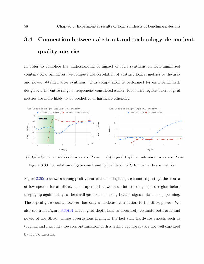
58 Chapter 3. Experimental results of logic synthesis of benchmark designs
3.4 Connection between abstract and technology-dependent
quality metrics
In order to complete the understanding of impact of logic synthesis on logic-minimized
combinatorial primitives, we compute the correlation of abstract logical metrics to the area
and power obtained after synthesis. This computation is performed for each benchmark
design over the entire range of frequencies considered earlier, to identify regions where logical
metrics are more likely to be predictive of hardware efficiency.
(a) Gate Count correlation to Area and Power (b) Logical Depth correlation to Area and Power
Figure 3.30: Correlation of gate count and logical depth of SBox to hardware metrics.
Figure 3.30(a) shows a strong positive correlation of logical gate count to post-synthesis area
at low speeds, for an SBox. This tapers off as we move into the high-speed region before
surging up again owing to the small gate count making LGC designs suitable for pipelining.
The logical gate count, however, has only a moderate correlation to the SBox power. We
also see from Figure 3.30(b) that logical depth fails to accurately estimate both area and
power of the SBox. These observations highlight the fact that hardware aspects such as
toggling and flexibility towards optimization with a technology library are not well-captured
by logical metrics.

3.4. Connection between abstract and technology-dependent quality metrics 59
Delay (ns)
Corr
elat
ion
-1
-0.5
0
0.5
1
2 3 4 5
N=8 N=12 N=16 N=20 N=22
Polynomial Multiplier - Correlation of Logical Gate Count to Area
(a) Gate Count correlation to Area
Delay (ns)
Corr
elat
ion
-1
-0.5
0
0.5
1
2 3 4 5
N=8 N=12 N=16 N=20 N=22
Polynomial Multiplier - Correlation of Logical Gate Count to Power
(b) Gate Count correlation to power
Figure 3.31: Correlation of logical gate count of polynomial multipliers to hardware metrics.
For a polynomial multiplier, we look at the correlation of gate count to area and power for
different values of N . It is clear that there is a pattern of the gate count being an accurate
estimator of area and power in the minimal-area region. The correlation drop at high speeds
happens sooner as the multiplier size increases, indicating the higher efficiency of matrix-
based alternatives for larger sizes. For power, it is evident that abstract metrics are highly
inaccurate for large multipliers throughout the delay range.
Delay (ns)
Corr
elat
ion
-1
-0.5
0
0.5
1
2.5 3 3.5 4 4.5 5
N=8 N=12 N=16 N=20 N=22
Polynomial Multiplier - Correlation of Logical Depth to Area
(a) Logical depth correlation to Area
Delay (ns)
Corr
elat
ion
-1
-0.5
0
0.5
1
2 3 4 5
N=8 N=12 N=16 N=20 N=22
Polynomial Multiplier - Correlation of Logical Depth to Power
(b) Logical depth correlation to power
Figure 3.32: Correlation of logical depth of polynomial multipliers to hardware metrics.
An interesting result is the correlation of logical depth to the area and power of polynomial
multipliers, shown in Figure 3.32. We see that at high speeds, while gate count fails to
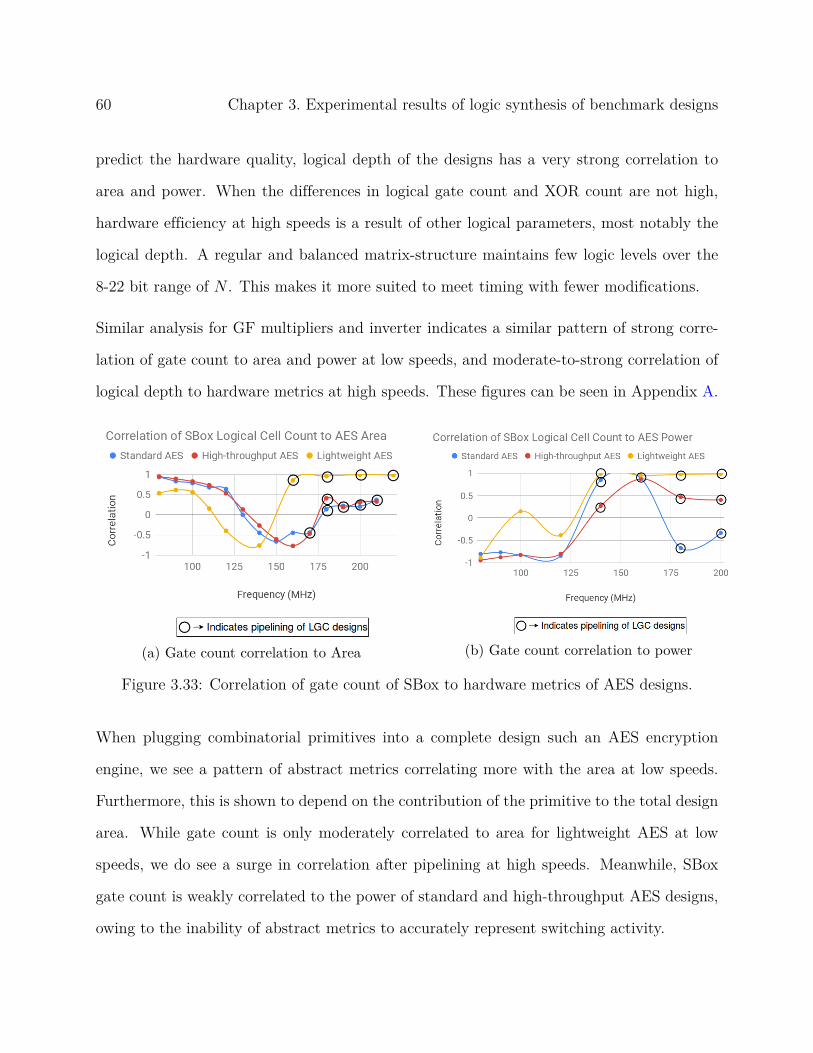
60 Chapter 3. Experimental results of logic synthesis of benchmark designs
predict the hardware quality, logical depth of the designs has a very strong correlation to
area and power. When the differences in logical gate count and XOR count are not high,
hardware efficiency at high speeds is a result of other logical parameters, most notably the
logical depth. A regular and balanced matrix-structure maintains few logic levels over the
8-22 bit range of N . This makes it more suited to meet timing with fewer modifications.
Similar analysis for GF multipliers and inverter indicates a similar pattern of strong corre-
lation of gate count to area and power at low speeds, and moderate-to-strong correlation of
logical depth to hardware metrics at high speeds. These figures can be seen in Appendix A.
(a) Gate count correlation to Area (b) Gate count correlation to power
Figure 3.33: Correlation of gate count of SBox to hardware metrics of AES designs.
When plugging combinatorial primitives into a complete design such an AES encryption
engine, we see a pattern of abstract metrics correlating more with the area at low speeds.
Furthermore, this is shown to depend on the contribution of the primitive to the total design
area. While gate count is only moderately correlated to area for lightweight AES at low
speeds, we do see a surge in correlation after pipelining at high speeds. Meanwhile, SBox
gate count is weakly correlated to the power of standard and high-throughput AES designs,
owing to the inability of abstract metrics to accurately represent switching activity.
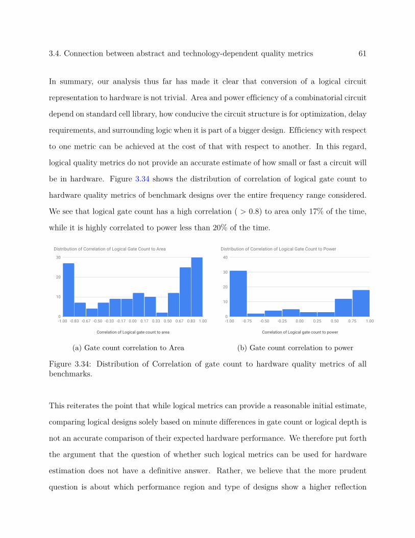
3.4. Connection between abstract and technology-dependent quality metrics 61
In summary, our analysis thus far has made it clear that conversion of a logical circuit
representation to hardware is not trivial. Area and power efficiency of a combinatorial circuit
depend on standard cell library, how conducive the circuit structure is for optimization, delay
requirements, and surrounding logic when it is part of a bigger design. Efficiency with respect
to one metric can be achieved at the cost of that with respect to another. In this regard,
logical quality metrics do not provide an accurate estimate of how small or fast a circuit will
be in hardware. Figure 3.34 shows the distribution of correlation of logical gate count to
hardware quality metrics of benchmark designs over the entire frequency range considered.
We see that logical gate count has a high correlation ( > 0.8) to area only 17% of the time,
while it is highly correlated to power less than 20% of the time.
Correlation of Logical gate count to area
0
10
20
30
-1.00 -0.83 -0.67 -0.50 -0.33 -0.17 0.00 0.17 0.33 0.50 0.67 0.83 1.00
Distribution of Correlation of Logical Gate Count to Area
(a) Gate count correlation to Area
Correlation of Logical gate count to power
0
10
20
30
40
-1.00 -0.75 -0.50 -0.25 0.00 0.25 0.50 0.75 1.00
Distribution of Correlation of Logical Gate Count to Power
(b) Gate count correlation to power
Figure 3.34: Distribution of Correlation of gate count to hardware quality metrics of allbenchmarks.
This reiterates the point that while logical metrics can provide a reasonable initial estimate,
comparing logical designs solely based on minute differences in gate count or logical depth is
not an accurate comparison of their expected hardware performance. We therefore put forth
the argument that the question of whether such logical metrics can be used for hardware
estimation does not have a definitive answer. Rather, we believe that the more prudent
question is about which performance region and type of designs show a higher reflection
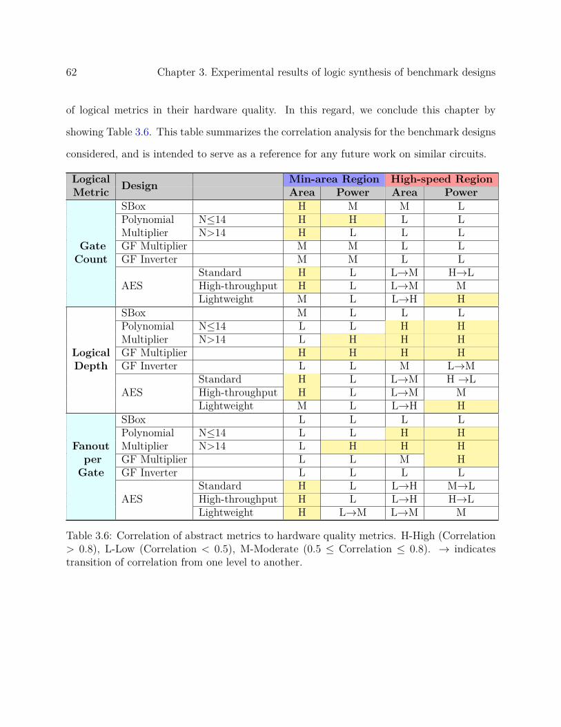
62 Chapter 3. Experimental results of logic synthesis of benchmark designs
of logical metrics in their hardware quality. In this regard, we conclude this chapter by
showing Table 3.6. This table summarizes the correlation analysis for the benchmark designs
considered, and is intended to serve as a reference for any future work on similar circuits.
Logical Min-area Region High-speed RegionMetric Design Area Power Area Power
SBox H M M LPolynomial N≤14 H H L LMultiplier N>14 H L L L
Gate GF Multiplier M M L LCount GF Inverter M M L L
Standard H L L→M H→LAES High-throughput H L L→M M
Lightweight M L L→H HSBox M L L LPolynomial N≤14 L L H HMultiplier N>14 L H H H
Logical GF Multiplier H H H HDepth GF Inverter L L M L→M
Standard H L L→M H →LAES High-throughput H L L→M M
Lightweight M L L→H HSBox L L L LPolynomial N≤14 L L H H
Fanout Multiplier N>14 L H H Hper GF Multiplier L L M H
Gate GF Inverter L L L LStandard H L L→H M→L
AES High-throughput H L L→H H→LLightweight H L→M L→M M
Table 3.6: Correlation of abstract metrics to hardware quality metrics. H-High (Correlation> 0.8), L-Low (Correlation < 0.5), M-Moderate (0.5 ≤ Correlation ≤ 0.8). → indicatestransition of correlation from one level to another.

Chapter 4
Design of prototype ASIC
This chapter presents the design of a prototype ASIC for benchmarking combinatorial logic-
minimized circuits on hardware. We begin with the reasons behind its architecture, followed
by integration of different hardware blocks onto this chip. We finally discuss the strategies
adopted for its physical design, ending with its post-layout evaluation.
4.1 Design Rationale
Having discussed how an SLP goes through logic synthesis in Chapter 3, the next step is to
come up with a suitable platform to benchmark the hardware performance of these designs.
While realizing these designs onto an ASIC is the obvious choice, simply grouping these
circuits together on a chip is of little or no benefit due to the following reasons:
• The design becomes pin-limited, i.e. a chip composed of simply a collection of these
combinatorial circuits would require an impractically large number of pins brought out of
it. This number grows out of control as the number of circuits increases, since each circuit
has eight or more inputs and outputs. This results in the chip boundary size growing just
to accommodate the pins, while the core itself is largely empty. This manifests into
inefficient area-utilization and lack of scalability.
• There is a lack of ease of user control for analysis. Having all the pins coming out of
63

64 Chapter 4. Design of prototype ASIC
the chip makes it mandatory for the circuits inside to be controlled through an external
voltage source connected to each pin of the circuit to be analyzed. This gives little or no
scope for automation that is essential to feed a large number of test vectors. Easy and
effective user control on such an ASIC becomes infeasible, and the chip itself is not very
flexible since its utility is limited to simply giving an output for a particular input sent.
The aforementioned reasons necessitate an elegant solution in the form of a central controlling
unit to access all the circuits to be benchmarked, while presenting a simple user interface for
feeding test vectors. This motivated us to opt for a processor-based System-on-Chip design.
Integrating hardware blocks onto such a design offers the following advantages:
• C programs - convenient user interface. The most attractive feature of using a processor
is the ease of running tests through simple-to-understand C programs. The user can now
work at a higher level of abstraction to access any hardware block of interest, since all of
them are connected to the processor through a common bus.
• Scalability - Hardware blocks are attached as “coprocessors” onto the system bus. Such
a hardware-software approach makes the entire design scalable in that any number of
additional independent hardware blocks can simply be attached to the bus through a
uniform interface for accessing them. We make use of this flexibility to add additional
cipher cores as hardware coprocessors for analysis.
4.2 SoC Architecture
The SoC designed in this project is referred to as “NISTCHIP”, and follows the ideas devel-
oped in a previous chip [51] that was designed in-house at the Secure Embedded Systems
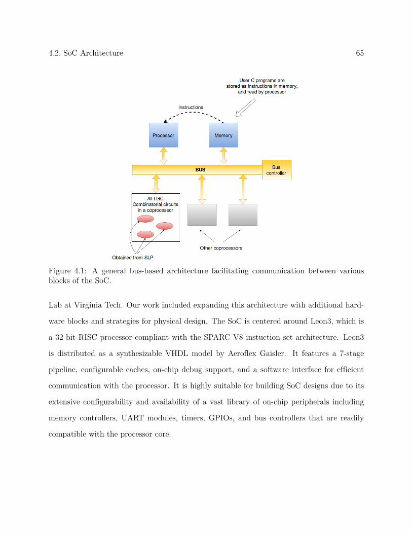
4.2. SoC Architecture 65
Figure 4.1: A general bus-based architecture facilitating communication between variousblocks of the SoC.
Lab at Virginia Tech. Our work included expanding this architecture with additional hard-
ware blocks and strategies for physical design. The SoC is centered around Leon3, which is
a 32-bit RISC processor compliant with the SPARC V8 instuction set architecture. Leon3
is distributed as a synthesizable VHDL model by Aeroflex Gaisler. It features a 7-stage
pipeline, configurable caches, on-chip debug support, and a software interface for efficient
communication with the processor. It is highly suitable for building SoC designs due to its
extensive configurability and availability of a vast library of on-chip peripherals including
memory controllers, UART modules, timers, GPIOs, and bus controllers that are readily
compatible with the processor core.

66 Chapter 4. Design of prototype ASIC
Figure 4.2: NISTCHIP Architecture
4.2.1 Memory-mapped coprocessors on NISTCHIP
Figure 4.2 shows the architecture of NISTCHIP. The processor is extensible through an
AMBA 2.0 bus system. It acts as a master on an Advanced High-performance Bus (AHB),
which also has a 128 KB on-chip RAM attached to it. The processor has access to all
peripherals through this system-wide bus. Hardware coprocessors are attached as “slaves”
onto an Advanced Peripheral Bus (APB) which is controlled by an APB controller (or APB
bridge) that is in turn attached as a slave to the AHB bus.

4.2. SoC Architecture 67
Each slave attached to a bus is treated by the processor as “memory”, and has an address
range associated with it. Any address in the range for a particular coprocessor is ignored by
all other blocks on the bus. Data to be written to a coprocessor is sent through the AHB
bus, transferred onto APB by an APB controller acting as a bridge, and finally written into
the coprocessor’s internal registers. Our chip splits the coprocessors over three APB bridges,
grouped according to functionality:
• APB Bridge 0 controls essential general-purpose peripherals including a hardware
timer, GPIOs, and UART controller.
• APB Bridge 1 controls electro-magnatic fault detection sensors [18], LR-Keymill
cipher, and an AES coprocessor with an LUT-SBox (denoted as AES-LUT).
• APB Bridge 2 controls of all other NISTCHIP-related coprocessors, listed below:
– The combinatorial modules obtained from SLPs, all grouped into one coprocessor
referred to as “NISTCOMB”.
– Reed-Solomon Encoder with an LGC circuit for state-update.
– AES coprocessors with LGC SBox and Wolkerstorfer SBox, referred to as AES-LGC
and AES-WOLK respectively.
– Direct Memory Access (DMA) controller for providing test vectors to NISTCOMB
at maximum speed.
– Three finalists of the “Competition for Authenticated Encryption: Security, Appli-
cability, and Robustness” (2014-2018), referred to as CAESAR [1]. These ciphers
include ACORN (32-bit and 8-bit datapath), AEGIS-128L, and MORUS-1280. De-
tailed discussion on the integration of these ciphers is provided in Chapter 5.
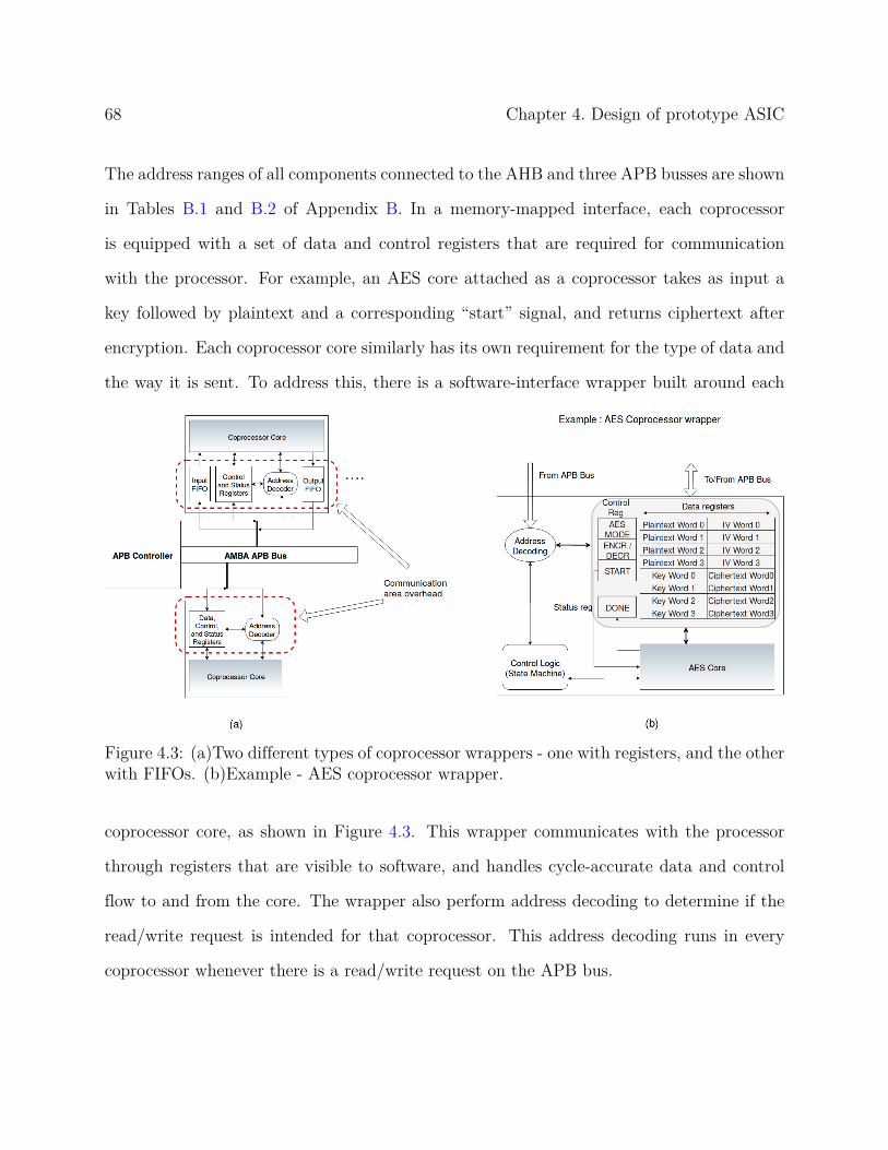
68 Chapter 4. Design of prototype ASIC
The address ranges of all components connected to the AHB and three APB busses are shown
in Tables B.1 and B.2 of Appendix B. In a memory-mapped interface, each coprocessor
is equipped with a set of data and control registers that are required for communication
with the processor. For example, an AES core attached as a coprocessor takes as input a
key followed by plaintext and a corresponding “start” signal, and returns ciphertext after
encryption. Each coprocessor core similarly has its own requirement for the type of data and
the way it is sent. To address this, there is a software-interface wrapper built around each
Figure 4.3: (a)Two different types of coprocessor wrappers - one with registers, and the otherwith FIFOs. (b)Example - AES coprocessor wrapper.
coprocessor core, as shown in Figure 4.3. This wrapper communicates with the processor
through registers that are visible to software, and handles cycle-accurate data and control
flow to and from the core. The wrapper also perform address decoding to determine if the
read/write request is intended for that coprocessor. This address decoding runs in every
coprocessor whenever there is a read/write request on the APB bus.

4.2. SoC Architecture 69
4.2.2 NISTCOMB coprocessor: Design and Programming model
The NISTCOMB coprocessor consists of combinatorial circuits obtained from SLPs, along
with a software-interface wrapper to control the input-output flow to each circuit. The
circuits included are listed in Table 4.1. Since all of them are combinatorial, their outputs
are available in a single clock cycle after sending an input. The wrapper consists of an input
and output FIFO for data storage. Once the input FIFO is filled with test vectors, they
are sent in consecutive cycles to the intended block, and the results are stored in the output
FIFO. Once the output FIFO is full, the wrapper asserts a status bit, and the results are
read out of the output FIFO. The presence of FIFOs is beneficial for data access through a
DMA, thereby facilitating data transfer at maximum speed without processor latency. The
coprocessor’s control register consists of bits to select the circuit that is desired to be active.
Since the combinatorial circuits in NISTCOMB are minute in area as compared to the rest
Component Name FunctionSBOX-LGC 8-bit LGC SBoxSBOX-LUT 8-bit LUT-based SBoxSBOX-WOLK 8-bit Wolkerstorfer SBox [46]INVSBOX-LGC 8-bit LGC Inverse SBoxINVSBOX-LUT 8-bit LUT-based Inverse SBoxINVSBOX-WOLK 8-bit Wolkerstorfer Inverse SBox [46]GF256MULT LGC GF (28) MultiplierGF65536MULT LGC GF (216) MultiplierGF256INV LGC GF (28) InverterK3LRSBOX 16-bit SBox [30]MULT64 64-bit LGC Polynomial multiplier
Table 4.1: Combinatorial circuits included in NISTCOMB coprocessor
of the design, multiple “instances” of them were created for better observation of their power
consumption (Figure 4.4). This also helps to average out differences due to design heuristics
while making area comparisons between (for example) the three SBox designs. The number
of instances can be four, two, or one, depending on the input width of the circuits.

70 Chapter 4. Design of prototype ASIC
Figure 4.4: Multiple instances of combinatorial blocks, depending on input width.
The complete software interface register space of NISTCOMB coprocessor are shown in
Tables B.3 - B.5 of Appendix B. The number of instances of each circuit that can be active
is controllable through a “redundancy” value in the control register. For example, inputs
of 8-bit blocks can be replicated from 1-4 times, whereas for a 16-bit block, inputs can be
replicated only twice.
4.3 NISTCHIP ASIC Design
Our prototype ASIC is designed using standard cells, IO pads, and bonding pads obtained
from TSMC 180nm technology library. The tools used at various stages of the design flow
are listed in Table 4.2.

4.3. NISTCHIP ASIC Design 71
Software Tool FunctionSynopsys Design Compiler (DC) Logic synthesis and DFT insertionSynopsys IC Compiler (ICC) Physical design (placement, routing, clock tree synthesis)Synopsys PrimeTime Post-synthesis and post-route power analysisMentor Graphics Calibre Chip verification and signoffMentor Graphics ModelSim RTL, post-synthesis, and post-route simulation
Table 4.2: Software tools used at various stages NISTCHIP design.
4.3.1 Logic synthesis of NISTCHIP
The complete design is synthesized at a frequency of 80 MHz, using slow-corner libraries to
consider worst-case delays. Due to the size of this SoC, and the large number of coprocessors,
synthesis is performed as an iterative process until the design meets timing. Appropriate
dont_touch and false_path constraints are set on legacy sensor modules that are a part of
this chip, in order to ensure that DC does not optimize their logic away. A useful strategy
followed to increase optimization on critical paths of the design was to add them to a separate
path group. Optimization by DC is now performed on the worst paths of each such path
group. The outcome of this strategy is an improvement in meeting timing constraints.
Synthesis is followed by insertion of scan chain. All registers in the coprocessors on APB
Bridge 2 that store their state, control, and status are added to the scan chain to increase
their observability. This is followed by incremental synthesis until the design is free of setup
violations. After the design is synthesized, gate-level simulation is performed to verify the
functionality of all coprocessors, after annotating worst-case post-synthesis delays through a
Standard Delay Format (SDF) file.

72 Chapter 4. Design of prototype ASIC
4.3.2 NISTCHIP Physical Design flow
The following subsections briefly discuss the important steps followed at different stages of
the physical design of NISTCHIP.
4.3.2.1 Floorplanning
The primary focus here is to fix the locations of all hard macros, and perform an initial coarse
placement of the design. We perform “virtual flat placement”, which considers the design to
be a flat collection of cells. Standard cells of each module are generally placed together, with
some overlap to account for interconnection between modules. Extra attention was given to
the following points during this stage:
• Macro proximity to relevant standard cells - To minimize wire-length of connections to
and from macros, it is important to ensure their physical proximity to standard cells they
are directly connected to. In this design, it was necessary to place the processor register
files close to the rest of the processor logic. After an initial run of coarse placement, the
rough location of the integer unit was understood to be close to instruction trace buffers
and cache memories that the processor requires access to. Fixing register files close to
this region aided in minimizing the number of critical paths.
• EM Sensor bounds - These sensors are built as a chain of large number of inverters and
multiplexers [18], to detect EM fault attacks that manifest as a clock glitch. As a result,
it was desired that the sensors remain compact, and the three flip flops in each such
sensor stay physically close together, with their clock signals preferably coming from the
same buffer. To accomplish this, exclusive move bounds were created for each sensor by
determining the rough area of a square they can fit in. Sensor locations were chosen
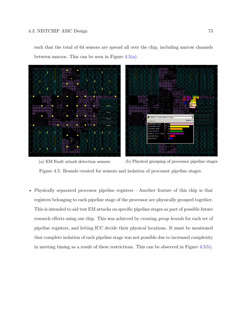
4.3. NISTCHIP ASIC Design 73
such that the total of 64 sensors are spread all over the chip, including narrow channels
between macros. This can be seen in Figure 4.5(a).
(a) EM Fault attack detection sensors (b) Physical grouping of processor pipeline stages
Figure 4.5: Bounds created for sensors and isolation of processor pipeline stages.
• Physically separated processor pipeline registers - Another feature of this chip is that
registers belonging to each pipeline stage of the processor are physically grouped together.
This is intended to aid test EM attacks on specific pipeline stages as part of possible future
research efforts using our chip. This was achieved by creating group bounds for each set of
pipeline registers, and letting ICC decide their physical locations. It must be mentioned
that complete isolation of each pipeline stage was not possible due to increased complexity
in meeting timing as a result of these restrictions. This can be observed in Figure 4.5(b).

74 Chapter 4. Design of prototype ASIC
4.3.2.2 Power Network Synthesis
Before creating the power grid on chip, power rings are first created around memory macros.
Pairs of macros were provided with a common ring to minimize unusable space under these
power rings. Route guides were created to ensure that power straps across the chip do not
pass too close to macro power rings. Power planning for the rest of the chip is then performed
using ICC’s automatic power network synthesis feature, with a power budget of 1000 mW
and a target IR drop of 100 mV . The number of width of straps was determined by the tool
based on these values. Finally, standard cell rows and macro power/ground rings are hooked
up to power/ground straps to complete the connection to each standard cell and macro.
Two-pass Synthesis Flow: At this point, floorplan and power network information of the
chip are saved, and the design is re-synthesized using DC in Topographical Mode. This is a
useful step to follow when the design is constrained by area. Knowledge of macro placement
and coarse physical locations of standard cells is used in this second-pass synthesis to make
further logic optimizations. This in turn potentially reduces area.
Figure 4.6: Power grid on chip, with power rings around pairs of macros.
4.3. NISTCHIP ASIC Design 75
4.3.2.3 Placement, Clock Tree Synthesis, and Routing
Placement of the design finalizes the location of each standard cell without any overlap. We
enable scan-chain optimization, which modifies the scan-chain based on physical proximity
as opposed to logical connections. This is followed by Clock Tree Synthesis (CTS). We make
use of clock buffer cells to initially build the clock tree, in order to avoid the tool’s pruning of
clock inverters during this process. Fixing of hold violations is enabled during CTS, making
use of fast-corner libraries to estimate best-case delays. Care is taken to ensure that the tool
performs Clock Reconvergence Pessimism Removal, in order to prevent over-constraining the
design. Optimization steps are performed repeatedly at the end of CTS to ensure that the
design stays free of major setup, hold, or logical design rule violations.
Following placement and CTS, all standard cells and macros are physically interconnected.
This chip is designed with six metal layers as provided by our technology library, with the
power/ground straps routed on the top two layers. Diode insertion is enabled to fix antenna
violations, with the rules and diode mode specified as defined by the technology vendor. We
run a single route_opt flow owing to its timing driven algorithms, and aggressive incremental
optimization to fix design rule violations. Due to high utilization of our available core area,
optimization runs after initial routing allowed partial placing of cells under power/ground
straps (with density of 25%), to provide a little extra space to move cells around.
4.3.2.4 Chip verification and signoff
Gate-level simulation is first performed to verify functionality of the netlist obtained after
placement and routing. Following this, the final step consists of verifying that vendor-
specified physical design rule constraints and antenna rules are met. Filler cells and metal
fillers are inserted to meet density requirements, followed by performing a Layout Versus

76 Chapter 4. Design of prototype ASIC
Schematic (LVS) check on the final layout using Mentor Graphics Calibre.
4.3.3 The final ASIC layout
Figure 4.7: Layout of the physically placed and routed chip.
Figure 4.7 shows the layout of the chip after physical placement and routing of the design.
Majority of the area is taken up by the on-chip RAM, with the Leon3 processor and co-
processors making up a substantial portion of the remaining area. The processor is placed
close to the register files and cache memory, while the physical location of the coprocessors
is not heavily dependent on any other block since they are all connected to a central APB
controller.

4.4. Post-layout results 77
4.4 Post-layout results
4.4.1 Area
The chip is to be fabricated on a 5mm × 5mm die, and the total core area occupied by
the design is 16.83 mm2. The 128K AHBRAM makes up 49% of this total area, while the
cache memories, processor register files, and instruction trace buffer make up an additional
8.6%. Figure 4.8 shows the area in terms of number of equivalent NAND2X1 gates of all
other blocks. While the coprocessors make up majority of the chip area, the APB and AHB
controllers do not account for a significant portion ( 0.6% of the total area).
Area
(KG
E)
0
50
100
150
200
Process
or Core
MMU ACache
MMU DCache
DMA
GP-Timer
AHB Controlle
r
APB Bridge 2
ACORN-32
ACORN-8
ReedSolomon
NISTCOMB
AES-LGC
AES-WOLK
AES-LUTAEGIS
MORUS
Keymill
Standalone
SBox senso
rs
Area (K Gate Eq.) of modules on chip
Figure 4.8: Area (K Gate Eq.) of individual blocks on chip
The areas of combinatorial circuits obtained from LGC SLPs are listed in Table 4.3.
4.4.2 Power Consumption
Power consumption of the chip is measured through a vector-based analysis for specific
coprocessor tests. These measurements are performed on the post-layout netlist, with the

78 Chapter 4. Design of prototype ASIC
Num. Area (mm2) NAND2X1 Gate Eq.Circuit Area (mm2) Instances per instance per instanceSBOX-LGC 0.0138 4 0.0034 345SBOX-LUT 0.0268 4 0.0067 672SBOX-WOLK 0.0145 4 0.0036 364INVSBOX-LGC 0.0158 4 0.0039 395INVSBOX-LUT 0.0245 4 0.0061 613INVSBOX-WOLK 0.0152 4 0.0038 381GF256MULT 0.0121 4 0.003 304GF65536MULT 0.021 2 0.0105 1050GF256INV 0.0115 4 0.0029 290GF65536INV 0.0259 2 0.013 1300K3LRSBOX 0.038 2 0.019 1910MULT64 0.0922 1 0.0922 9240
Table 4.3: Post-layout area of combinatorial circuits on NISTCHIP
interconnect parasitics annotated on the design through a SPEF file obtained from ICC. Both
the chip-level power and hierarchical block-level power consumed over the total simulation
duration are obtained from analysis using PrimeTime. Two different coprocessor tests are
discussed below.
4.4.2.1 NISTCOMB Test - SBox power comparison
A set of 256 random test vectors is sent to each of the three SBox circuits present in NIST-
COMB. These vectors are sent in groups of 32, as the FIFOs in NISTCOMB can hold upto
32 vectors at a time. Table 4.6 shows the power consumption of each SBox.
SBOX-LGC Test SBOX-LUT Test SBOX-WOLK TestSBox Power 0.282 mW 0.248 mW 0.314 mW
NISTCOMB Power 15.1 mW 15.0 mW 15.1 mW
Table 4.4: Post-layout power consumption of SBox circuits in NISTCOMB - 256 test vectorsfed through DMA.
An important point regarding power consumption is that the overall chip-level power is a

4.4. Post-layout results 79
result of not just a single coprocessor. In a processor-based SoC, there are multiple compo-
nents on the chip that are active at the same time, and hence can contribute to total power.
For this particular SBox test, it was found that the clock network on chip contributes to
56% of total chip-level power. The contribution of major active SoC components during a
NISTCOMB test is listed in Table 4.5 below.
Component on Chip Power (mW ) % of Total PowerTop-level 331 100%
Processor Core 19.2 5.8%DMA 12.5 3.8%
Cache controller 2.155 0.6%AHB Controller 0.928 0.3%APB Bridge 2 0.796 0.2%
NISTCOMB Coprocessor 15.0-15.1 4.5-4.6%
Table 4.5: Contribution of components on SoC to total power during NISTCOMB test.
It can be seen that although there is a difference of around 20% power within the SBoxes,
this hardly reflects in total power or even the coprocessor power. At the coprocessor level,
power due to the communication overhead in the form of FIFOs overshadows that of the
combinatorial blocks, while at the chip level, even the coprocessor power is a small fraction
due to clock network and other active components. This goes on to show that when integrated
with a big system, individual combinatorial blocks has a negligible impact on total power.
4.4.2.2 AES Test
This test feeds 64 blocks of plaintext into each of the three AES coprocessors running en-
cryption in CBC mode. The power consumption of different components active during this
test is listed in Table 4.7 below.
In summary, this chapter discussed the prototype ASIC designed for benchmarking of com-
binatorial logic-minimized circuits. A processor-based SoC was used as a platform for this

80 Chapter 4. Design of prototype ASIC
AES-LGC AES-LUT AES-WOLK19.8 mW 19.2 mW 19.0 mW
Table 4.6: Post-layout power consumption of AES circuits - encryption of 64 plain-textblocks in CBC mode.
Component on Chip Power (mW ) % of Total PowerTop-level 323 100%
Processor Core 25.2 7.8%Cache controller 2.773 0.8%AHB Controller 0.688 0.2%APB Bridge 2 0.611 0.2%
AES Coprocessor 19.8 6.1%
Table 4.7: Contribution of components on SoC to total power during AES Tests.
purpose, and additional cryptographic blocks were added as coprocessors. The next chapter
presents extensive analysis on the AEAD coprocessors integrated on this SoC.
Chapter 5
Impact of SoC integration on
Authenticated Encryption Ciphers
5.1 Introduction
Authenticated Encryption has gained popularity as a hardware-efficient and secure alter-
native to two-phase algorithms employing separate encryption and message authentication
[19]. The fundamental idea is to use a single cipher that provides authenticity in addition
to confidentiality and integrity. Authenticated Encryption with Associated Data (AEAD)
schemes take a message or plaintext (PT) as input along with a key, associated data (AD),
and a public message number (Npub). Following encryption of the message, a tag is gen-
erated that is used to verify authenticity during decryption. CAESAR [1] has been driving
the development of new AEAD ciphers for lightweight and high-performance applications.
As was mentioned in Chapter 4, we picked three of the CAESAR finalists to be integrated
as hardware coprocessors onto our SoC.
The motivation behind this work is that such an integration incurs non-negligible impact
on the area, power, and performance of the ciphers, examples of which were provided in
[23]. Extensive analysis of hardware implementations of the AEAD ciphers can be found in
literature [21, 29, 31]. However, existing works consider these ciphers as standalone hardware
blocks, and the results do not always hold when they are integrated on to a larger system.
81

82 Chapter 5. Impact of SoC integration on Authenticated Encryption Ciphers
For example, Figure 5.1 (similar to Figure 4.3 in Chapter 4) is shown here to reiterate the fact
that plugging a hardware block onto a system bus requires wrapper logic for communication.
Since the penalty in resources brought about by this additional logic is unavoidable, it is
up to the designers to choose a scheme that can appropriately minimize overhead in area,
power, and performance.
Figure 5.1: A generic wrapper structure for an AEAD coprocessor on Leon3-based SoC.
As with any hardware design, there is no golden method for building a coprocessor. The SoC
integration scheme used on our chip is only one of different methods that result in varying
amount of overhead. Hence, it would not be fair to generalize our results from the post-layout
analysis of our chip. Our aim here is to explore multiple alternatives for wrapper design that
take advantage of the way the cipher cores work, and underline the benefits of each design
alternative. We provide our comments on which of those is likely to be of practical utility
in an SoC context, and the trade-offs to be considered in the process.
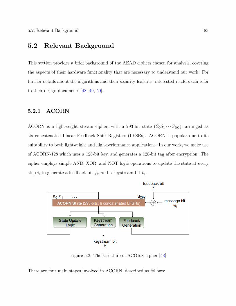
5.2. Relevant Background 83
5.2 Relevant Background
This section provides a brief background of the AEAD ciphers chosen for analysis, covering
the aspects of their hardware functionality that are necessary to understand our work. For
further details about the algorithms and their security features, interested readers can refer
to their design documents [48, 49, 50].
5.2.1 ACORN
ACORN is a lightweight stream cipher, with a 293-bit state (S0S1 · · ·S292), arranged as
six concatenated Linear Feedback Shift Registers (LFSRs). ACORN is popular due to its
suitability to both lightweight and high-performance applications. In our work, we make use
of ACORN-128 which uses a 128-bit key, and generates a 128-bit tag after encryption. The
cipher employs simple AND, XOR, and NOT logic operations to update the state at every
step i, to generate a feedback bit fi, and a keystream bit ki.
Figure 5.2: The structure of ACORN cipher [48]
There are four main stages involved in ACORN, described as follows:

84 Chapter 5. Impact of SoC integration on Authenticated Encryption Ciphers
• Initialization: The initialization stage consists of loading the key and Initialization
Vector (IV) bit-by-bit to update the state. Initialization runs for 1792 steps in total.
Figure 5.3: Message stream during ACORN initialization
• Processing Associated Data: In this stage, the associated data is used to update the
state. Considering an AD of size adlen bits, this stage first runs for adlen steps. This is
followed by 256 additional steps which are mandatory even when the length of AD is 0.
Figure 5.4: ACORN message stream during AD processing
• Encryption: In addition to using plaintext to update the state, this stage generates a
ciphertext bit by XOR-ing the corresponding plaintext and keystream bits. Similar to
the previous stage, this stage also runs a mandatory 256 additional steps after processing
ptlen bits of plaintext. When ptlen is 0, there is no ciphertext generated.
Figure 5.5: ACORN message stream during PT encryption
• Finalization: The final stage involves generating the tag by running for 768 steps in
total. The last 128 keystream bits form the 128-bit tag. The message bit is set to 0
throughout this stage.
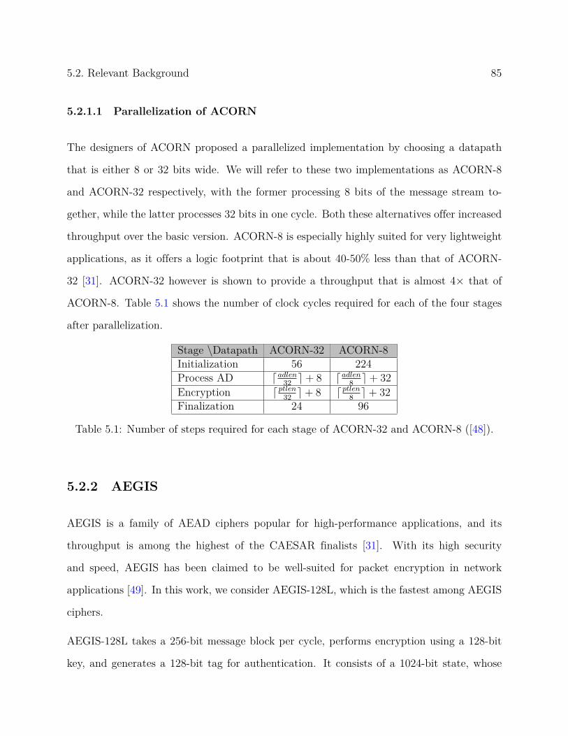
5.2. Relevant Background 85
5.2.1.1 Parallelization of ACORN
The designers of ACORN proposed a parallelized implementation by choosing a datapath
that is either 8 or 32 bits wide. We will refer to these two implementations as ACORN-8
and ACORN-32 respectively, with the former processing 8 bits of the message stream to-
gether, while the latter processes 32 bits in one cycle. Both these alternatives offer increased
throughput over the basic version. ACORN-8 is especially highly suited for very lightweight
applications, as it offers a logic footprint that is about 40-50% less than that of ACORN-
32 [31]. ACORN-32 however is shown to provide a throughput that is almost 4× that of
ACORN-8. Table 5.1 shows the number of clock cycles required for each of the four stages
after parallelization.
Stage \Datapath ACORN-32 ACORN-8Initialization 56 224Process AD ⌈adlen
32⌉+ 8 ⌈adlen
8⌉+ 32
Encryption ⌈ptlen32
⌉+ 8 ⌈ptlen8
⌉+ 32Finalization 24 96
Table 5.1: Number of steps required for each stage of ACORN-32 and ACORN-8 ([48]).
5.2.2 AEGIS
AEGIS is a family of AEAD ciphers popular for high-performance applications, and its
throughput is among the highest of the CAESAR finalists [31]. With its high security
and speed, AEGIS has been claimed to be well-suited for packet encryption in network
applications [49]. In this work, we consider AEGIS-128L, which is the fastest among AEGIS
ciphers.
AEGIS-128L takes a 256-bit message block per cycle, performs encryption using a 128-bit
key, and generates a 128-bit tag for authentication. It consists of a 1024-bit state, whose

86 Chapter 5. Impact of SoC integration on Authenticated Encryption Ciphers
Figure 5.6: AEGIS-128L state update - Each Si is a 128-bit word of the state [49].
update logic consists of eight AES round functions as shown in Figure 5.6. An important
distinction from ACORN is that there is no state update performed when the length of AD
or PT is 0. Padding on the data, if any, is performed externally before sending it to the core.
Moreover, the block size here is greater, which results in reduced number of computation
steps for the same data size. It is easy to observe that the high throughput and security
comes at the expense of higher area resulting from high parallelization and multiple AES
round functions.
Stage Number of cyclesInitialization 10Process AD ⌈adlen
256⌉
Encryption ⌈ptlen256
⌉Finalization 7
Table 5.2: Number of clock cycles required for each stage of AEGIS-128L.
There are four stages in AEGIS-128L with similar functionality as those of ACORN, but the
algorithm differs in the time taken for each stage. A wider datapath and absence of padding
by the core also contribute to its high speed. This is summarized in Table 5.2.

5.3. Design alternatives for SoC integration 87
5.2.3 MORUS
The MORUS family of AEAD ciphers is designed following the manner of stream cipher
design which involves low-complex state-update functions [50]. The design is intended to be
fast in both hardware and software, especially in the absence of AES-NI instruction. MORUS
can be viewed as a design offering parts of the benefits of both AEGIS and ACORN:
• High throughput due to 256-bit messages, absence of padding steps, and small number of
steps in each stage of the algorithm, all of which are similar to AEGIS.
• State-update with small logic footprint similar to ACORN, employing simple AND, XOR,
and rotation operations.
Stage Number of cyclesInitialization 16Process AD ⌈adlen
256⌉
Encryption ⌈ptlen256
⌉Finalization 8
Table 5.3: Number of clock cycles required for each stage of MORUS-128L.
Its hardware efficiency stems from its replacing of AES round functions for state-update
with simpler logic. As a result, MORUS achieves the best throughput-to-area ratio among
the CAESAR finalists [31]. The parameters used in our analysis are those of MORUS-1280,
making use of a 128-bit key, 1280-bit state, and 256-message block. Table 5.3 lists the
number of computation steps required for each stage of MORUS.
5.3 Design alternatives for SoC integration
As was shown in Figure 5.1, there are two main components in the coprocessor wrapper:

88 Chapter 5. Impact of SoC integration on Authenticated Encryption Ciphers
• Storage elements for core signals: For the AEAD cipher coprocessors used here,
registers are required to store the key, public data, input message, and the results in the
form of cipher-text and tag. In addition, registers are also needed to store the size of AD
and PT, but these are small in size and negligible in comparison to the data registers
required.
• Control logic to send/receive data to/from the core: This logic is generally mod-
eled as a Finite State Machine (FSM) that waits for the required inputs to be received
by the wrapper before sending them to the core, ensuring appropriate handshaking as
required by the core. Similarly, it needs to monitor the results from the core to be stored
and sent out to the system bus when requested.
The control logic is fundamental to the functioning of a coprocessor wrapper, and is therefore
unavoidable. Moreover, the FSM itself is not as important to the overhead as the storage
is. This is simply due to the fact that the FSM consists of only a few bits of state and
combinatorial state-update logic, whereas the storage of data consists of large number of flip
flops, which is likely to have significant effect in a lightweight context. We therefore narrow
down our analysis to three design alternatives depending on the size of storage resources
making up the wrapper.
5.3.1 An intuitive and convenient wrapper design - FIFOs at the
input and output
This is a simple scheme where the processor continuously sends all data to the coprocessor
which stores them in a FIFO at the input side. The control FSM in the wrapper monitors
the core and reads data out of the input FIFO as and when the core is ready to accept them.
The ciphertext and tag sent out of the core are stored in a FIFO on the output side. The

5.3. Design alternatives for SoC integration 89
software monitors the completion of encryption and tag generation before reading the result
out.
Figure 5.7: Illustration of Coprocessor wrapper and Software API for integration with inputand output FIFOs.
Advantages: This method effectively decouples the cipher core and the processor by en-
abling continuous data transfer from the processor. There is little or no handshaking required
between the wrapper and the processor since data loss will be avoided by the presence of
the input FIFO. This method does not require the coprocessor designer to understand the
cipher core in great detail apart from the interface signals and handshaking mechanism.
Disadvantages: The FIFOs take up too much space. For instance, with the TSMC 180 nm
library used for this chip, even a small 64-word (2KBit) FIFO built with flip flops is about
2.5× bigger than the entire ACORN core. While it can be argued that replacing flip flops
with SRAM memory macros could be a better alternative, we found that a 64-word (2KBit)
SRAM macro for TSMC 180nm technology still takes up 1.7× more space than the core.
Another notable disadvantage of using FIFOs is that it limits the amount of data that can
be sent to the coprocessor at one go. Failure to maintain the FIFO read rate greater than
or equal to that of the write rate can potentially lead to data loss depending on the size of
data. A possible workaround is to send the data in installments, reading the results for one

90 Chapter 5. Impact of SoC integration on Authenticated Encryption Ciphers
group of data words before sending the next.
5.3.2 Reducing wrapper overhead - FIFO only at the output
What the area numbers in the previous subsection go on to show is that even small FIFOs
manifest as a huge overhead when added on top of a compact cipher core, so much so that
the coprocessor as a whole no longer retains the lightweight properties of the core. Removing
one of the FIFOs is therefore appealing since it can halve the FIFO overhead. This is further
made possible by the fundamental working of the AEAD cipher cores.
As was described in Section 5.2, these ciphers require only one cycle to process a particular
message (AD or PT), generate the ciphertext, and get ready to accept the next word. The
only wait periods when the core cannot accept inputs occur during initialization and final-
ization stages. What this means is that apart from the wait periods, reading data from the
input FIFO can happen as fast as the rate at which data is written. This can be exploited
by creating a scheme where there is no input FIFO, and data that is sent through software
is forwarded to the core immediately. The software needs to perform handshaking with the
wrapper during the wait periods, since no data is sent to the core in this duration.
Advantages: The basic functionality of the core lends itself well to this scheme. While
the extra handshaking is expected to result in a small performance penalty, the primary
advantage here is the huge reduction in area and power made possible by getting rid of one
entire FIFO.
Disadvantages: This method requires greater understanding of the cipher core’s hardware
implementation than the previous scheme. For instance, for the ciphers here, small mod-
ifications were required to ensure that the cipher core does not assume that AD and PT
inputs arrive at consecutive cycles. The extent of complexity of these changes depend on the

5.3. Design alternatives for SoC integration 91
Figure 5.8: Illustration of Coprocessor wrapper and Software API for integration with onlyan output FIFO.
cipher used and its hardware implementation. In addition, this scheme still does not solve
the problem of a limit on the maximum size of data that can be sent at once. Since there is
still one FIFO present, data of size greater than the FIFO’s capacity needs to be sent over
installments.
5.3.3 Lightweight integration - no FIFOs in the wrapper
This scheme makes use of a no-frills wrapper with no FIFOs to hold data. This uses only reg-
isters to hold the key and public data, along with a 128-bit (or 256-bit, for AEGIS/MORUS)
message word at the input and the output. The intention here is to consider this design as
a reference that indicates the best-case scenario, i.e. an estimate on the lower bound for the
wrapper overhead.
While this scheme minimizes wrapper overhead, it requires changes on the software side. It
is now not possible to send more than 128 (or 256) bits of data before reading the result
out, since there is no FIFO at the output of the core. Therefore, this scheme requires the
software to send four (or eight) 32-bit words of data, followed by an immediate reading of

92 Chapter 5. Impact of SoC integration on Authenticated Encryption Ciphers
four (or eight) ciphertext words. This is repeated until the whole message is encrypted.
Figure 5.9: Illustration of Coprocessor wrapper and Software API for lightweight integrationwith no FIFOs.
Advantages: As mentioned earlier, this design presents a good example of the minimum
wrapper overhead that is unavoidable for a particular cipher. If implemented in a practical
system, this design is not expected to be significantly slower than the other schemes when all
data is sent only by the processor. This is because the number of read and write operations
are still the same, with only the order changed.
Disadvantages: When compared with designs that send data in a burst (for example,
through Direct Memory Access), this scheme is bound to have a lower performance, since
it cannot support bursty data. In that sense, the practical utility of this scheme is lim-
ited. Furthermore, for ciphers that require more than one cycle to generate the result, this
scheme will require constant polling by the software to monitor when the operation is done,
before reading the result out. This can lead to decreased throughput and increased power
consumption.

5.4. Evaluation Methodology 93
5.3.4 Direct Memory Access (DMA) for increased throughput
While presenting the performance of a coprocessor, care must be taken to show both the
best-case and worst-case scenarios. While sending inputs from the processor is a simple
method, it incurs significant loss in performance due to each data transfer going through
the processor pipeline as an individual instruction. A common method followed in practical
designs is to offload the task of transferring large data to a DMA controller that simply reads
a large chunk of data from a source and writes it to a destination.
As there is a DMA controller already included in our SoC, we consider transfers to the
coprocessors through DMA, in order to understand the best-case performance achievable
after SoC integration. This can be used with the first two FIFO schemes described earlier,
and is very beneficial in systems that already have a DMA controller as part of the SoC.
5.4 Evaluation Methodology
Separate coprocessor wrappers with an APB interface are first built for each type of wrapper
discussed, and the design alternatives that are analyzed are as follows:
1. Input and Output FIFOs, with and without DMA for ACORN-8, ACORN-32, AEGIS,
and MORUS.
2. Output FIFO only, with and without DMA for ACORN-32, AEGIS, and MORUS.
3. No FIFO, without DMA for ACORN-32, AEGIS, and MORUS.
94 Chapter 5. Impact of SoC integration on Authenticated Encryption Ciphers
5.4.1 Studying Area and Power
For the purpose of analysis, all the coprocessor alternatives are attached to the APB bus
on the SoC, and the design is synthesized at 80 MHz using Synopsys DC with the same
constraints as those on our primary chip design. We obtain the post-synthesis area from
DC to understand the “price to pay” for SoC integration, i.e. how much additional area is
required over the standalone cipher core.
To study power efficiency, gate-level simulation is first run on the post-synthesis netlist for
each design alternative using ModelSim. The test cases used here include those provided by
the designers, as well as a set of arbitrary test vectors of different sizes. VCD files generated
from ModelSim are used for power analysis using Synopsys PrimeTime. We focus primarily
on dynamic power consumption of the top-level design, the coprocessor, and other active
components of the SoC. Static power being three orders of magnitude smaller in the 180 nm
technology node, is not included here due to its negligible impact on total power.
5.4.2 Performance Analysis
Performance comparison is performed through RTL simulation in Modelsim with test cases
of different sizes, using the general-purpose timer present on the SoC to measure clock cycles
elapsed from the start of an encryption to its end. Following similar analysis previously pre-
sented in literature [23], we observe that total time required for an authenticated encryption
using a coprocessor on an SoC can be broken down into the following components:
• Computation Time: Time required for the hardware coprocessor to complete the entire
authenticated encryption.
• Communication Time: This refers to the total time required for sending data and

5.5. Observations and Results 95
control words to the coprocessor, and reading the results back. Communication time is
composed of two types of overhead:
– Bus Overhead: Time taken for data transfer to and from coprocessor over the system
bus.
– Processor overhead: Time spent in the processor pipeline, which includes instruction
decoding, cache operations, and memory accesses.
For the AEAD ciphers considered in this work, a major part of computation time overlaps
with communication time due to their single-cycle state updates. The only non-overlapped
portion occurs when the software waits for final tag generation to be completed after sending
all data. This is illustrated in Figure 5.10. The contributions of each type of overhead will
be presented in the following section.
Figure 5.10: An example of different sources of contribution to the total time for authenti-cated encryption using an AEAD coprocessor on SoC.
5.5 Observations and Results
In this section, we now discuss important results from our analysis of coprocessor alternatives,
and provide our comments on the benefits and trade-offs they pose at the system-level.

96 Chapter 5. Impact of SoC integration on Authenticated Encryption Ciphers
5.5.1 ACORN-32
5.5.1.1 Area and Performance
Figure 5.11(a) first shows that even with the most lightweight wrapper with no FIFOS, there
is still a 1.7× increase in area over the ACORN-32 core. The storage elements needed for
the key and data are comparable in size to the internal logic of ACORN-32, making the
resultant coprocessor significantly bigger. Furthermore, adding two 1 KBit FIFOs is seen to
be highly area-inefficient, resulting in a 4× increase in area.
Figure 5.11(b) shows the performance comparison of the different coprocessor alternatives,
represented as the ratio of the time consumed for each design, with the time required for
standalone hardware. First, we see that in addition to saving 30% area, having only an output
FIFO incurs only a small performance loss of less than 5% as compared to a conventional
two-FIFO design. This decrease in performance arises due to the additional wait period
required for the former as shown in Figure 5.12. However, as this duration is fixed, the loss
in performance remains small over all the test cases.
Another important observation from Figure 5.11(b) is that the DMA-based design alterna-
tives are slower for message smaller than 32 bytes, while they provide significant speedup
for longer messages. The increased speedup for large messages is because the DMA mini-
mizes processor overhead which is the dominant component of total time consumed. The
DMA controller reads data from RAM in consecutive cycles before transferring them to the
coprocessor without any processor intervention in between (Figure 5.13).
DMA-based design alternatives perform worse for small data sizes since there is a fixed time
required to program the DMA each time it transfers a block of data. This task consumes
more time than the actual data transfer. This point is highlighted in Figure 5.14, where the

5.5. Observations and Results 97
Area
(K G
ate
Eq)
0
10
20
30
40
ACORN core ACORN coprocessor - NO
FIFO
Acorn Coprocessor - Output FIFO
ACORN Coprocessor -
Input and Output FIFOs
ACORN-32: Coprocessor Area Comparison
(a) Area overhead.
Performance improved by DMA
(b) Performance overhead - lower value indicates better performance.
Figure 5.11: Area and performance overhead of ACORN-32 coprocessor alternatives.
contribution of processor overhead when using DMA is seen to be close to 75% of total time
for small messages. For larger data, this contribution progressively decreases to less than
60% of total time by using DMA, whereas it remains consistently above 67% without DMA.
Considering the fact that this happens only for very small data sizes, we believe that using
DMA is beneficial in order to extract the best possible performance in a practical setting.
Finally, Figure 5.11(b) suggests that the FIFO-less no-frills design maintains appreciable

98 Chapter 5. Impact of SoC integration on Authenticated Encryption Ciphers
(a) Two-FIFO design
(b) Output-FIFO-only design
Figure 5.12: Illustration of communication overhead and wait periods.
Figure 5.13: Reduction of processor overhead in data transfer using DMA.
performance that is better than the designs not using DMA. The reason is that this design
sends four data words in quick succession before reading four words of ciphertext. The
processor overhead caused due to loop operations is smaller here, as opposed to FIFO-based
designs. For larger test cases, the performance of this design does not drop as sharply as
other non-DMA designs, and remains within 10% of the DMA-based alternatives. In Figure
5.11(b), it becomes faster than DMA-based designs for message sizes between 240-330 bytes.
This is because the data is sent across two DMA transfers owing to FIFO limitations.
To summarize this analysis of area and performance, we make use of throughput-per-area as

5.5. Observations and Results 99
AD + PT Length (Bytes)
% o
f Tot
al T
ime
0%
25%
50%
75%
100%
8 6 10 16 24 31 32111
120140
170190
220239
271324
384430
Processor Overhead Bus Overhead Computation Overhead
ACORN-32: Computation-Communication overhead split, Without DMA
(a) Designs not employing DMAAD + PT Length (Bytes)
% o
f Tot
al T
ime
0%
25%
50%
75%
100%
8 6 10 16 24 31 32111
120140
170190
220239
271324
384430
Processor Overhead Bus Overhead Computation Overhead
ACORN-32: Computation-Communication overhead split, With DMA
(b) Designs using DMA
Figure 5.14: ACORN-32 coprocessor performance - Computation, communication overhead.
(AD+PT) Length (Bytes)
Thro
ughp
ut (M
bps)
/ Ar
ea (K
GE)
0
5
10
15
0 100 200 300 400
Two FIFOs, no DMA Output-FIFO, no DMA No FIFO Two FIFOs, DMAOutput-FIFO, DMA
ACORN-32: Coprocessor Throughput-per-Area
Figure 5.15: Throughput-per-area of ACORN-32 coprocessor designs.
a metric that captures both the performance and silicon overhead together. This is shown
for all the designs in Figure 5.15. Averaged over all tests, the lightweight no-FIFO wrapper
wins with a 1.63× higher throughput-per-area over the next best design. For systems where
the use of DMA is desired, the output-FIFO wrapper provides the best trade-off.

100 Chapter 5. Impact of SoC integration on Authenticated Encryption Ciphers
5.5.1.2 Power and Energy efficiency
The overall power consumed by an SoC during a particular coprocessor operation is affected
by switching in the active coprocessor, as well as other active components on the chip. These
blocks, which are necessary for the SoC’s basic functionality, mainly include the processor,
memories, system bus, and the cache controller. As an illustration, Table 5.4 lists the
contribution of these major components to the total SoC power for an ACORN-32 test using
DMA.
Component on Chip % of Total powerOn-Chip Memory 25.71%Processor 8.0%ACORN-32 Coprocessor 7.1%DMA Controller 3.7%Cache controller 0.8%AHB 0.3%APB 0.3%
Table 5.4: Contribution of active blocks to total power during ACORN-32 tests.
Block Clock Tree power (% of block power)Top-level 59.8%Processor 62.1%ACORN-32 Coprocessor
With FIFOs 82.2%Without FIFOs 65.04%
DMA Controller 27.6%Cache controller 27.55%
Table 5.5: Contribution of clock tree to block-level power during ACORN-32 tests.
From Table 5.4, we see that apart from memory, the processor and active coprocessor have a
significant contribution. The busses and cache controller have very small impact on the total
power due to their relatively lower hardware footprint. In addition, Table 5.5 shows that for
the major blocks, a large part of their power consumption comes from their clock tree. This

5.5. Observations and Results 101
is due to constant switching of the clock network and related buffers, and this becomes more
pronounced with the increase in the size of the block. We now discuss how different design
alternatives affect the power of active blocks, and their impact on total power.
Pow
er (W
)
0.23
0.235
0.24
0.245
0.25
0.255
2 FIFOs, no DMA
Output FIFO, no DMA
No FIFO 2 FIFOs, DMA Output FIFO, DMA
Top-level Power - ACORN-32 Test
(a) Top-level power consumption
Pow
er (W
)0.00E+00
1.00E-02
2.00E-02
3.00E-02
Processor ACORN-32 Coprocessor
ACORN32-FIFO ACORN32-Core DMA
2 FIFOs, no DMA Output FIFO, no DMA No FIFO 2 FIFOs, DMA Output FIFO, DMA
Block Level Power - ACORN-32 Test
(b) Block-level power consumption
Figure 5.16: Power consumption resulting from different ACORN-32 coprocessor designs.
Figure 5.16(a) shows that the DMA-based designs result in a 3.6% increase of chip-level
(top-level) power, computed over the total simulation duration. The reason for this small
impact is the domination of clock power that results in reduced visibility of dynamic power
due to logic switching during coprocessor tests. Since the impact on top-level power greatly
depends on SoC size, number of simultaneously active components on chip, and the extent
of clock or power gating, we additionally focus on block-level power consumption (Figure
5.16(b)).
While the DMA-based designs result in 16% less processor power due to reduced activity, the
power consumption due to the DMA controller and its internal buffers offsets this difference.
As for integration overhead on the cipher core, we see that ACORN-32 is a wrapper-limited
design, with the FIFO power contributing to 59% and 42% of total coprocessor power for
the two-FIFO and one-FIFO designs respectively. As a result, the no-FIFO wrapper gives
the most power-efficient ACORN-32 coprocessor. However, the most power-efficient copro-
cessor does not necessarily result in the least power at the system level since the coprocessor

102 Chapter 5. Impact of SoC integration on Authenticated Encryption Ciphers
amounts to less than 5% of top-level power. In this regard, it is the one-FIFO wrapper
without DMA that is seen to result in smallest top-level power. The reason for this is its
significantly smaller run-time as compared to other alternatives, which brings our focus onto
energy-efficiency as an alternate quality metric.
Ener
gy p
er b
it (n
J/bi
t)
0
5
10
15
20
2 FIFOs, no DMA
Output FIFO, no
DMA
No FIFO 2 FIFOs, DMA
Output FIFO, DMA
Top-level Energy-per-bit - ACORN-32 Test, Small messages
(a) Top-level energy for small messages
Ener
gy p
er B
it (n
J/bi
t)
0.00E+00
5.00E-01
1.00E+00
1.50E+00
2.00E+00
Processor ACORN-32 Coprocessor
ACORN32-FIFO ACORN32-Core DMA
2 FIFOs, no DMA Output FIFO, no DMA No FIFO 2 FIFOs, DMA Output FIFO, DMA
Block-level Energy-per-bit - ACORN-32 Test, Small messages
(b) Block-level energy for small messages
Ener
gy p
er B
it (n
J/bi
t)
1.5
1.75
2
2.25
2.5
2 FIFOs, no DMA
Output FIFO, no
DMA
No FIFO 2 FIFOs, DMA
Output FIFO, DMA
Top-level Energy-per-bit - ACORN-32 Test, Large messages
(c) Top-level energy for large messages
Ener
gy p
er B
it (n
J/bi
t)
0.00E+00
5.00E-02
1.00E-01
1.50E-01
2.00E-01
2.50E-01
Processor ACORN-32 Coprocessor
ACORN-32 FIFO
ACORN-32 Core
DMA
2 FIFOs, no DMA Output FIFO, no DMA No FIFO 2 FIFOs, DMAOutput FIFO, DMA
Block-level Energy-per-bit - ACORN-32 Test, Large messages
(d) Block-level energy for large messages
Figure 5.17: Energy efficiency of ACORN-32 coprocessor alternatives.
The need to compare energy-efficiency is two-fold. First, embedded applications running
on battery-powered devices are required to consume lesser energy over time. Second, the
design alternatives considered differ significantly in their run-time, making power comparison
misleading due to its being averaged over time. Figures 5.17(a) and 5.17(b) show the DMA-
based designs being the least energy-efficient for small messages. Excess time spent in
DMA programming as compared to data transfer, as was discussed in Section 5.5.1.1, is

5.5. Observations and Results 103
the reason for this inefficiency. Figures 5.16(a) and 5.16(b) indicate that for more practical
message lengths, DMA-based designs reduce top-level energy consumption per message bit
by 20%, owing to their faster completion. Another interesting result is that the no-FIFO
wrapper offers comparable energy-efficiency to the DMA-based designs at the top-level, while
reducing the ACORN-32 coprocessor energy-per-bit by more than 36% for all message sizes
considered. This is due to a combination of power reduction due to speed comparable to
DMA-based designs (shown in Section 5.5.1.1), and complete elimination of FIFO power.
We summarize this analysis by suggesting that unless the message sizes are extremely small,
using DMA with FIFO-based wrappers or the lightweight no-FIFO wrapper are the most
energy-efficient options for ACORN-32.
5.5.2 ACORN-8
5.5.2.1 Area and Performance
Figure 5.18(a) shows the most important result here - there is a severe area penalty incurred
during the SoC integration of a lightweight cipher with a shortened datapath width. The
coprocessor wrappers needs to be able to write 32-bit data per cycle, while it can only
read out 8 bits at a time. Furthermore, there is a large initialization time of 224 cycles
when no data can be read out of the FIFO. With the FIFO-less lightweight wrapper not
being suitable here, the coprocessor area becomes 6.4× that of the cipher core. This clearly
negates the primary intention of making the cipher lightweight. Regarding performance,
with the ACORN-8 core being inherently much slower than the other ciphers (Table 5.1),
SoC integration makes it 1.6-2× slower. Using a DMA is better for performance, providing
a 1.2× increase over the non-DMA alternative.
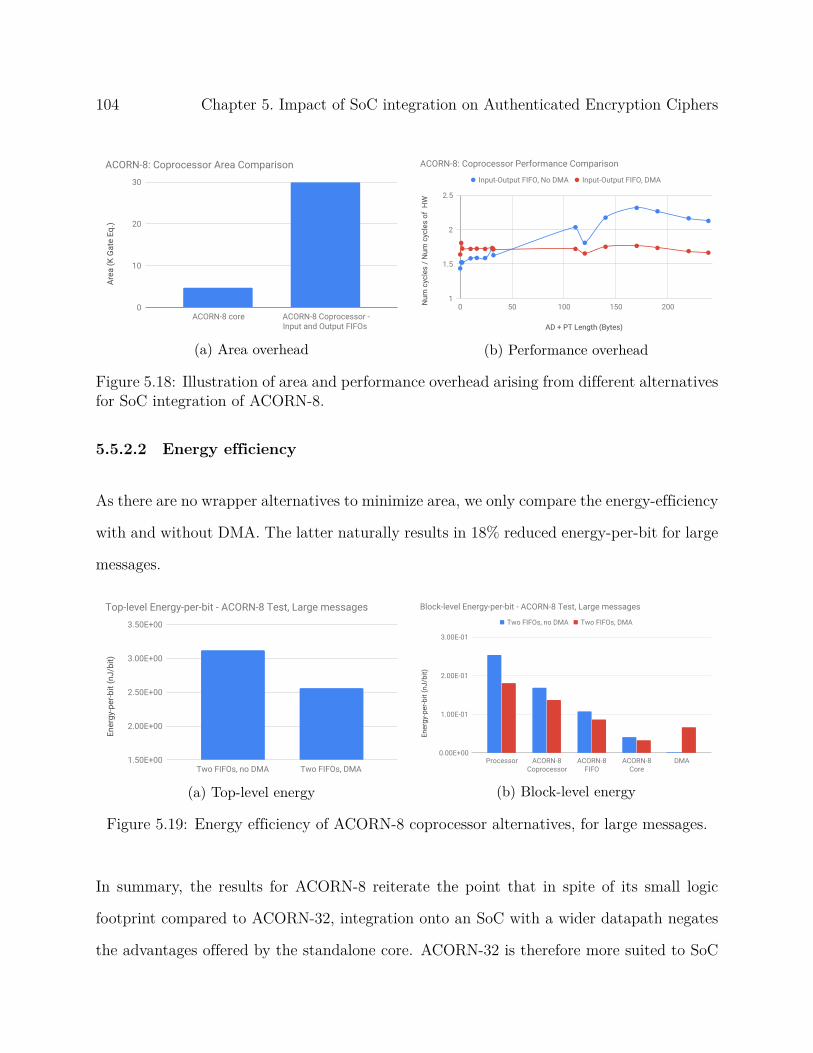
104 Chapter 5. Impact of SoC integration on Authenticated Encryption CiphersAr
ea (K
Gat
e Eq
.)
0
10
20
30
ACORN-8 core ACORN-8 Coprocessor - Input and Output FIFOs
ACORN-8: Coprocessor Area Comparison
(a) Area overheadAD + PT Length (Bytes)
Num
cyc
les
/ Num
cyc
les
of H
W
1
1.5
2
2.5
0 50 100 150 200
Input-Output FIFO, No DMA Input-Output FIFO, DMA
ACORN-8: Coprocessor Performance Comparison
(b) Performance overhead
Figure 5.18: Illustration of area and performance overhead arising from different alternativesfor SoC integration of ACORN-8.
5.5.2.2 Energy efficiency
As there are no wrapper alternatives to minimize area, we only compare the energy-efficiency
with and without DMA. The latter naturally results in 18% reduced energy-per-bit for large
messages.
Ener
gy-p
er-b
it (n
J/bi
t)
1.50E+00
2.00E+00
2.50E+00
3.00E+00
3.50E+00
Two FIFOs, no DMA Two FIFOs, DMA
Top-level Energy-per-bit - ACORN-8 Test, Large messages
(a) Top-level energy
Ener
gy-p
er-b
it (n
J/bi
t)
0.00E+00
1.00E-01
2.00E-01
3.00E-01
Processor ACORN-8 Coprocessor
ACORN-8 FIFO
ACORN-8 Core
DMA
Two FIFOs, no DMA Two FIFOs, DMA
Block-level Energy-per-bit - ACORN-8 Test, Large messages
(b) Block-level energy
Figure 5.19: Energy efficiency of ACORN-8 coprocessor alternatives, for large messages.
In summary, the results for ACORN-8 reiterate the point that in spite of its small logic
footprint compared to ACORN-32, integration onto an SoC with a wider datapath negates
the advantages offered by the standalone core. ACORN-32 is therefore more suited to SoC

5.5. Observations and Results 105
integration than ACORN-8.
5.5.3 AEGIS-128L
5.5.3.1 Area and Performance
The area of AEGIS-128L coprocessor is heavily influenced by its core, as opposed to lightweight
ciphers like ACORN, whose core in comparison is about 14× smaller. This can be understood
from Figure 5.20(a), which shows the AEGIS-128L coprocessor area to be affected more by
its core than the wrapper. Adding a small 512-bit input FIFO and a 2 KBit output FIFO
has only a 1.31× area overhead. A small input FIFO is sufficient since the FIFO is read
immediately after every eight writes to it due to the 256-bit message block size. A FIFO-less
wrapper adds 9.8% additional area to the AEGIS-128L core, while a two-FIFO design adds
31% overhead. Doing away with the input FIFO provides a negligible area reduction of 4%.
Area
K G
ate
Eq.)
0
50
100
150
200
AEGIS-128L Core AEGIS-128L Coprocessor - No
FIFO
AEGIS-128L Coprocessor - Output FIFO
AEGIS-128L Coprocessor -
Input and Ouput FIFOs
AEGIS-128L: Coprocessor Area Comparison
(a) Area overheadAD + PT Length (Bytes)
Num
cyc
les
/ Num
cyc
les
of H
W
0
20
40
60
0 100 200 300 400
Input-Output FIFO, No DMA Output FIFO, No DMA No FIFO, No DMAInput-Output FIFO, DMA Output FIFO, DMA
AEGIS-128L: Coprocessor Performance comparison
(b) Performance overhead
Figure 5.20: Illustration of area and performance overhead arising from different alternativesfor SoC integration of AEGIS-128L.
The coprocessor performance follows a similar pattern as that for ACORN, but the decrease
in speed over a standalone hardware implementation is more pronounced due to the high
speed of AEGIS-128L. As a result, the best-case performance on SoC obtained using a DMA

106 Chapter 5. Impact of SoC integration on Authenticated Encryption Ciphers
is still 30-35× slower than standalone AEGIS-128L hardware. The performances of the two
FIFO-based designs are almost identical due to very small wait periods between stages.
AD+PT Length (Bytes)
Thro
ughp
ut (M
bps)
/ Ar
ea (K
GE)
0
0.5
1
1.5
2
0 100 200 300 400
Two FIFOs, no DMA Output-FIFO, no DMA No FIFO Two FIFOs, DMAOutput-FIFO, DMA
AEGIS-128L: Coprocessor Throughput-per-Area
Figure 5.21: Throughput-per-area of AEGIS-128L coprocessor designs.
In summary, from Figure 5.21, we conclude that the no-FIFO wrapper and the FIFO-based
wrappers using DMA all provide appreciable area-performance trade-off. The output-FIFO
design has a higher throughput-per-area for larger messages, but only by a small factor of
1.07×. This goes on to suggest that the choice of wrapper does not have a significant impact
on bulky ciphers such as AEGIS.
5.5.3.2 Power and Energy efficiency
An important observation here is that the AEGIS coprocessor contributes 12.6% to the total
power, which is higher than even that of the processor. The contributions of other blocks to
total power are close to those seen in the ACORN tests, and are listed in Appendix C. The
large logic footprint of AEGIS leads to high clock network power, and the highly parallelized
implementation causes increased logic switching power. Unlike ACORN, the AEGIS core
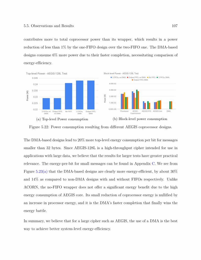
5.5. Observations and Results 107
contributes more to total coprocessor power than its wrapper, which results in a power
reduction of less than 1% by the one-FIFO design over the two-FIFO one. The DMA-based
designs consume 6% more power due to their faster completion, necessitating comparison of
energy-efficiency.
Pow
er (W
)
0.22
0.225
0.23
0.235
0.24
0.245
2 FIFOs, no DMA
Output FIFO, no DMA
No FIFO 2 FIFOs, DMA
Output FIFO, DMA
Top-level Power - AEGIS-128L Test
(a) Top-level Power consumption
Pow
er (W
)
0.00E+00
1.00E-02
2.00E-02
3.00E-02
4.00E-02
Processor AEGIS - Coprocessor
AEGIS-FIFO AEGIS-Core DMA
2 FIFOs, no DMA Output FIFO, no DMA No FIFO 2 FIFOs, DMAOutput FIFO, DMA
Block-level Power - AEGIS-128L Test
(b) Block-level power consumption
Figure 5.22: Power consumption resulting from different AEGIS coprocessor designs.
The DMA-based designs lead to 20% more top-level energy consumption per bit for messages
smaller than 32 bytes. Since AEGIS-128L is a high-throughput cipher intended for use in
applications with large data, we believe that the results for larger tests have greater practical
relevance. The energy-per-bit for small messages can be found in Appendix C. We see from
Figure 5.23(a) that the DMA-based designs are clearly more energy-efficient, by about 30%
and 14% as compared to non-DMA designs with and without FIFOs respectively. Unlike
ACORN, the no-FIFO wrapper does not offer a significant energy benefit due to the high
energy consumption of AEGIS core. Its small reduction of coprocessor energy is nullified by
an increase in processor energy, and it is the DMA’s faster completion that finally wins the
energy battle.
In summary, we believe that for a large cipher such as AEGIS, the use of a DMA is the best
way to achieve better system-level energy-efficiency.
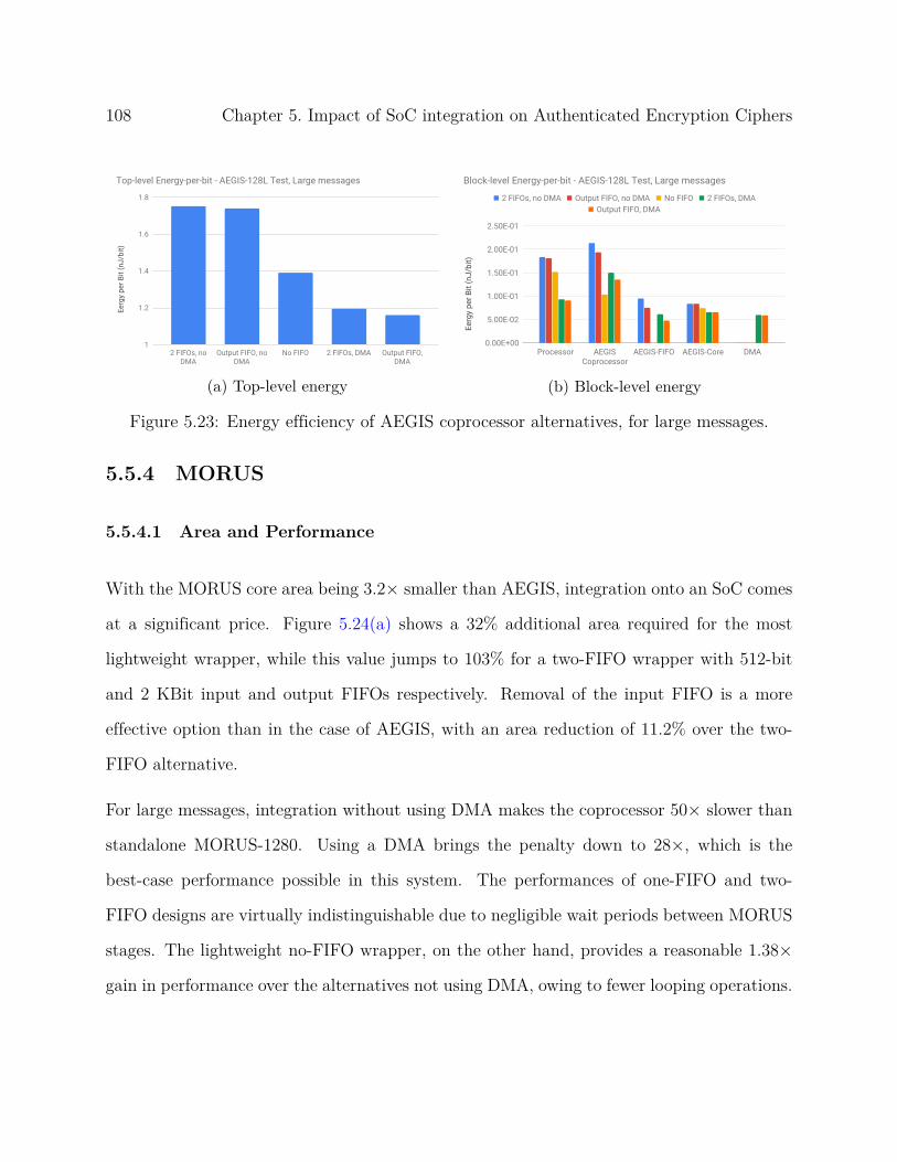
108 Chapter 5. Impact of SoC integration on Authenticated Encryption CiphersEe
rgy
per B
it (n
J/bi
t)
1
1.2
1.4
1.6
1.8
2 FIFOs, no DMA
Output FIFO, no DMA
No FIFO 2 FIFOs, DMA Output FIFO, DMA
Top-level Energy-per-bit - AEGIS-128L Test, Large messages
(a) Top-level energy
Eerg
y pe
r Bit
(nJ/
bit)
0.00E+00
5.00E-02
1.00E-01
1.50E-01
2.00E-01
2.50E-01
Processor AEGIS Coprocessor
AEGIS-FIFO AEGIS-Core DMA
2 FIFOs, no DMA Output FIFO, no DMA No FIFO 2 FIFOs, DMAOutput FIFO, DMA
Block-level Energy-per-bit - AEGIS-128L Test, Large messages
(b) Block-level energy
Figure 5.23: Energy efficiency of AEGIS coprocessor alternatives, for large messages.
5.5.4 MORUS
5.5.4.1 Area and Performance
With the MORUS core area being 3.2× smaller than AEGIS, integration onto an SoC comes
at a significant price. Figure 5.24(a) shows a 32% additional area required for the most
lightweight wrapper, while this value jumps to 103% for a two-FIFO wrapper with 512-bit
and 2 KBit input and output FIFOs respectively. Removal of the input FIFO is a more
effective option than in the case of AEGIS, with an area reduction of 11.2% over the two-
FIFO alternative.
For large messages, integration without using DMA makes the coprocessor 50× slower than
standalone MORUS-1280. Using a DMA brings the penalty down to 28×, which is the
best-case performance possible in this system. The performances of one-FIFO and two-
FIFO designs are virtually indistinguishable due to negligible wait periods between MORUS
stages. The lightweight no-FIFO wrapper, on the other hand, provides a reasonable 1.38×
gain in performance over the alternatives not using DMA, owing to fewer looping operations.
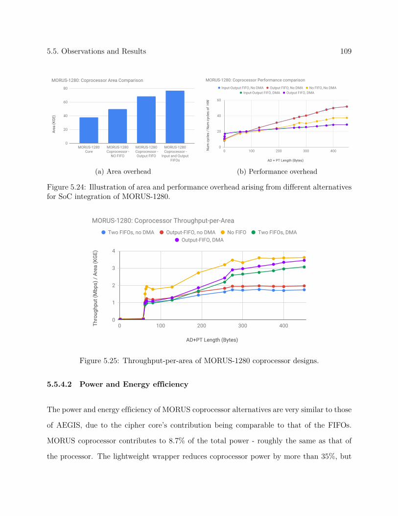
5.5. Observations and Results 109Ar
ea (K
GE)
0
20
40
60
80
MORUS-1280 Core
MORUS-1280 Coprocessor -
NO FIFO
MORUS-1280 Coprocessor - Output FIFO
MORUS-1280 Coprocessor -
Input and Output FIFOs
MORUS-1280: Coprocessor Area Comparison
(a) Area overheadAD + PT Length (Bytes)
Num
cyc
les
/ Num
cyc
les
of H
W
0
20
40
60
0 100 200 300 400
Input-Output FIFO, No DMA Output FIFO, No DMA No FIFO, No DMAInput-Output FIFO, DMA Output FIFO, DMA
MORUS-1280: Coprocessor Performance comparison
(b) Performance overhead
Figure 5.24: Illustration of area and performance overhead arising from different alternativesfor SoC integration of MORUS-1280.
AD+PT Length (Bytes)
Thro
ughp
ut (M
bps)
/ Ar
ea (K
GE)
0
1
2
3
4
0 100 200 300 400
Two FIFOs, no DMA Output-FIFO, no DMA No FIFO Two FIFOs, DMAOutput-FIFO, DMA
MORUS-1280: Coprocessor Throughput-per-Area
Figure 5.25: Throughput-per-area of MORUS-1280 coprocessor designs.
5.5.4.2 Power and Energy efficiency
The power and energy efficiency of MORUS coprocessor alternatives are very similar to those
of AEGIS, due to the cipher core’s contribution being comparable to that of the FIFOs.
MORUS coprocessor contributes to 8.7% of the total power - roughly the same as that of
the processor. The lightweight wrapper reduces coprocessor power by more than 35%, but

110 Chapter 5. Impact of SoC integration on Authenticated Encryption Ciphers
increases that of the processor, thereby leading to a 3.3% increase in top-level power. As
seen in previous ciphers, DMA-based designs increase top-level power by 4-5%.
Pow
er (W
)
2.85E-01
2.90E-01
2.95E-01
3.00E-01
3.05E-01
3.10E-01
3.15E-01
2 FIFOs, no DMA
Output FIFO, no
DMA
No FIFO 2 FIFOs, DMA
Output FIFO, DMA
Top-level Power - MORUS-1280 Test
(a) Top-level Power consumptionPo
wer
(W)
0.00E+00
1.00E-02
2.00E-02
3.00E-02
Processor MORUS Coprocessor
MORUS-FIFO MORUS-Core DMA
2 FIFOs, no DMA Output FIFO, no DMA No FIFO 2 FIFOs, DMAOutput FIFO, DMA
Block-level Power - MORUS-1280 Test
(b) Block-level power consumption
Figure 5.26: Power consumption resulting from different AEGIS coprocessor designs.
Energy consumed per message bit for small messages has been plotted for different MORUS
coprocessor alternatives in Appendix C. They are not discussed here since MORUS, like
AEGIS, is aimed at providing high performance which is practically more relevant for mes-
sages larger than 32 bytes. DMA-based design alternatives are energy-efficient for large mes-
sages, leading to 16.4% energy reduction per message bit over the no-FIFO design. While the
latter eliminates FIFO energy, the cipher core itself amounts to roughly half the coprocessor
power. In addition, the processor energy is increased by the no-FIFO design, due to which
it leads to an increase in overall top-level energy consumption.
5.6 Conclusion
With one-pass AEAD ciphers gaining traction due to their high speed and hardware-efficiency,
the relative lack of research on their integration onto a System-on-Chip motivated the analy-
sis in this chapter. Different coprocessor alternatives for CAESAR finalists ACORN, AEGIS,
and MORUS were studied with regard to their area, performance, and power after SoC in-
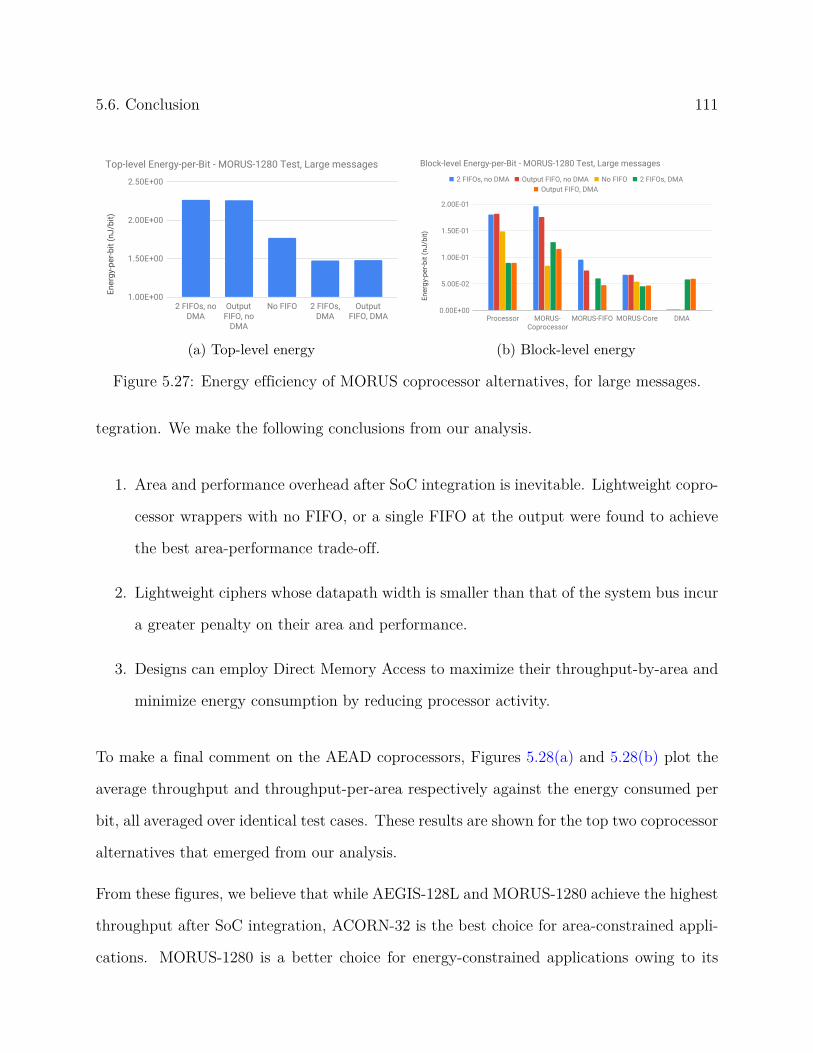
5.6. Conclusion 111En
ergy
-per
-bit
(nJ/
bit)
1.00E+00
1.50E+00
2.00E+00
2.50E+00
2 FIFOs, no DMA
Output FIFO, no
DMA
No FIFO 2 FIFOs, DMA
Output FIFO, DMA
Top-level Energy-per-Bit - MORUS-1280 Test, Large messages
(a) Top-level energy
Ener
gy-p
er-b
it (n
J/bi
t)
0.00E+00
5.00E-02
1.00E-01
1.50E-01
2.00E-01
Processor MORUS- Coprocessor
MORUS-FIFO MORUS-Core DMA
2 FIFOs, no DMA Output FIFO, no DMA No FIFO 2 FIFOs, DMAOutput FIFO, DMA
Block-level Energy-per-Bit - MORUS-1280 Test, Large messages
(b) Block-level energy
Figure 5.27: Energy efficiency of MORUS coprocessor alternatives, for large messages.
tegration. We make the following conclusions from our analysis.
1. Area and performance overhead after SoC integration is inevitable. Lightweight copro-
cessor wrappers with no FIFO, or a single FIFO at the output were found to achieve
the best area-performance trade-off.
2. Lightweight ciphers whose datapath width is smaller than that of the system bus incur
a greater penalty on their area and performance.
3. Designs can employ Direct Memory Access to maximize their throughput-by-area and
minimize energy consumption by reducing processor activity.
To make a final comment on the AEAD coprocessors, Figures 5.28(a) and 5.28(b) plot the
average throughput and throughput-per-area respectively against the energy consumed per
bit, all averaged over identical test cases. These results are shown for the top two coprocessor
alternatives that emerged from our analysis.
From these figures, we believe that while AEGIS-128L and MORUS-1280 achieve the highest
throughput after SoC integration, ACORN-32 is the best choice for area-constrained appli-
cations. MORUS-1280 is a better choice for energy-constrained applications owing to its

112 Chapter 5. Impact of SoC integration on Authenticated Encryption Ciphers
MORUS, Output-FIFO, DMA
AEGIS, No FIFO
AEGIS, Output-FIFO, DMA
ACORN-32, No FIFO
ACORN-32,Output-FIFO, DMA
ACORN-8, TwoFIFOs, DMA
MORUS, No FIFO
(a) Throughput vs Energy-per-bit
MORUS, Output-FIFO, DMA
AEGIS, No FIFO
AEGIS, Output-FIFO, DMA
ACORN-32, No FIFO
ACORN-32,Output-FIFO, DMA
ACORN-8, TwoFIFOs, DMA
MORUS, No FIFO
(b) Throughput-per-area vs Energy-per-bit
Figure 5.28: Comparison of AEAD coprocessors.
better throughput-per-area than AEGIS-128L.

Chapter 6
Conclusion
This thesis presented the impact of logic synthesis on circuits minimized by a new class
of tools optimized for low gate count. The hardware efficiency of circuits was extensively
compared with that of a set of benchmark designs over a range of frequencies, after synthesis,
as well as physical design. This analysis was performed to demonstrate the importance of
trade-offs between the circuits’ area, power, and performance after synthesis. Specific regions
in the solution space were highlighted, where logic minimization provides intended benefits
on hardware. Furthermore, it was also shown that these benefits are liable to diminish
when logic-minimized combinatorial blocks are integrated with a complete system. This
discussion ends with a study of overall effectiveness of using logical metrics to predict the
aforementioned circuits’ hardware efficiency. A prototype ASIC was designed to observe the
performance and efficiency of these circuits on hardware. The ASIC comprises a System-on-
Chip designed to accommodate multiple hardware blocks as coprocessors around a Leon3
processor core. Apart from a coprocessor consisting of logic-minimized circuits, the SoC
also includes recently developed ciphers for authenticated encryption. The second part of
this thesis explored the implementation of these ciphers as coprocessors on an SoC, and
investigated the benefits and trade-offs associated with different design alternatives for the
same. We believe that the results presented in this thesis will serve as a useful reference for
future research in this field.
113

Bibliography
[1] CAESAR: Competition for Authenticated Encryption: Security, Applicability, and Ro-
bustness. https://competitions.cr.yp.to/caesar.html.
[2] Hardware implementation of finite-field arithmetic. http://www.
arithmetic-circuits.org/finite-field/vhdl_codes.htm.
[3] Tohoku university: Cryptographic Hardware Project, May 2015. URL http://www.
aoki.ecei.tohoku.ac.jp/crypto/.
[4] Kazumaro Aoki, Tetsuya Ichikawa, Masayuki Kanda, Mitsuru Matsui, Shiho Moriai,
Junko Nakajima, and Toshio Tokita. Camellia: A 128-bit block cipher suitable for
multiple platforms - design and analysis. In Selected Areas in Cryptography, 2000.
[5] Christof Beierle, Thorsten Kranz, and Gregor Leander. Lightweight multiplication in
GF(2n) with applications to MDS Matrices. In Matthew Robshaw and Jonathan Katz,
editors, Advances in Cryptology – CRYPTO 2016, pages 625–653, Berlin, Heidelberg,
2016. Springer Berlin Heidelberg. ISBN 978-3-662-53018-4.
[6] Daniel J. Bernstein. Minimum number of bit operations for multiplication. https:
//binary.cr.yp.to/m.html.
[7] Daniel J. Bernstein. Batch Binary Edwards. In CRYPTO, 2009.
[8] Joan Boyar and René Peralta. A New Combinational Logic Minimization Technique
with Applications to Cryptology. In Festa P. (eds) Experimental Algorithms. SEA 2010.
Lecture Notes in Computer Science, volume 6049. Springer, Berlin, Heidelberg, 2010.
114

BIBLIOGRAPHY 115
[9] Joan Boyar and René Peralta. A Small Depth-16 Circuit for the AES S-Box. In Gritzalis
D., Furnell S., Theoharidou M. (eds) Information Security and Privacy Research. SEC
2012. IFIP Advances in Information and Communication Technology. Springer, Berlin,
Heidelberg, 2012.
[10] Joan Boyar, Morris Dworkin, René Peralta, Meltem Turan, Cagdas Calik, , and Luis
Brandao. Circuit minimization work. http://cs-www.cs.yale.edu/homes/peralta/
CircuitStuff/CMT.html. Past collaborators include: Michael Bartock, Ramon Col-
lazo, Magnus Find, Michael Fischer, Murat Cenk, Christopher Wood, Andrea Visconti,
Chiara Schiavo, Holman Gao, Bruce Strackbein, Larry Bassham.
[11] Joan Boyar, Philip Matthews, and René Peralta. Logic minimization techniques with
applications to cryptology. J. Cryptol., 26(2):280–312, April 2013. ISSN 0933-2790. doi:
10.1007/s00145-012-9124-7. URL http://dx.doi.org/10.1007/s00145-012-9124-7.
[12] Joan Boyar, Magnus Find, and René Peralta. Small low-depth circuits for cryptographic
applications. Cryptography and Communications, 11:109–127, 2018.
[13] David Canright. A very compact Rijndael S-box, 2004. URL https://calhoun.nps.
edu/handle/10945/791.
[14] David Canright. A very compact s-box for aes. In CHES, 2005.
[15] Murat Cenk and M. Anwar Hasan. Some new results on binary polynomial multiplica-
tion. Cryptology ePrint Archive, Report 2015/094, 2015. https://eprint.iacr.org/
2015/094.
[16] Alessandro Cilardo. Fast parallel GF(2m) polynomial multiplication for all degrees.
IEEE Transactions on Computers, 62:929–943, 2013.

116 BIBLIOGRAPHY
[17] Nicolas Courtois, Daniel Hulme, and Theodosis Mourouzis. Solving circuit optimisation
problems in cryptography and cryptanalysis. IACR Cryptology ePrint Archive, 2011:
475, 01 2011.
[18] Chinmay Deshpande. Hardware fault attack detection methods for secure embedded
systems. Master’s Thesis, Computer Engineering, Virginia Tech, February 2018. URL
https://vtechworks.lib.vt.edu/handle/10919/82141.
[19] William Diehl, Farnoud Farahmand, Abubakr Abdulgadir, Jens-Peter Kaps, and Kris
Gaj. Face-off between the CAESAR lightweight finalists: ACORN vs. Ascon. Cryptol-
ogy ePrint Archive, Report 2019/184, 2019. https://eprint.iacr.org/2019/184.
[20] Michele Elia, M Leone, and C Visentin. Low complexity bit-parallel multipliers for
GF(2m) with generator polynomial xm + xk + 1. Electronics Letters, 35:551 – 552, 05
1999. doi: 10.1049/el:19990407.
[21] Farnoud Farahmand, William Diehl, Abubakr Abdulgadir, Jens-Peter Kaps, and Kris
Gaj. Improved lightweight implementations of CAESAR Authenticated Ciphers. 2018
IEEE 26th Annual International Symposium on Field-Programmable Custom Computing
Machines (FCCM), pages 29–36, 2018.
[22] Carsten Fuhs and Peter Schneider-Kamp. Synthesizing shortest Linear Straight-Line
Programs over gf(2) using SAT. In Ofer Strichman and Stefan Szeider, editors, Theory
and Applications of Satisfiability Testing – SAT 2010, pages 71–84, Berlin, Heidelberg,
2010. Springer Berlin Heidelberg. ISBN 978-3-642-14186-7.
[23] Xu Guo, Zhimin Chen, and Patrick Schaumont. Energy and performance evaluation
of an FPGA-Based SoC platform with AES and PRESENT coprocessors. In Embedded
Computer Systems: Architectures, Modeling, and Simulation, pages 106–115, Berlin,
Heidelberg, 2008. Springer Berlin Heidelberg. ISBN 978-3-540-70550-5.

BIBLIOGRAPHY 117
[24] Alper Halbutogullari and Cetin Koc. Mastrovito multiplier for general irreducible poly-
nomials. IEEE Trans. Computers, 49:503–518, 01 2000.
[25] Jingwei Hu, Wei Guo, Jizeng Wei, and Ray C. C. Cheung. Fast and generic inversion
architectures over gf(2m) using modified Itoh–Tsujii algorithms. IEEE Transactions
on Circuits and Systems II: Express Briefs, 62:367–371, 2015.
[26] José Luis Imaña, Román Hermida, and Francisco Tirado. Low complexity bit-parallel
multipliers based on a class of irreducible pentanomials. IEEE Transactions on Very
Large Scale Integration (VLSI) Systems, 14:1388–1393, 2006.
[27] Jérémy Jean, Thomas Peyrin, and Siang Meng Sim. Optimizing implementations of
lightweight building blocks. IACR Trans. Symmetric Cryptol., 2017:130–168, 2017.
[28] Sanu K. Mathew, Farhana Sheikh, Michael Kounavis, Shay Gueron, Amit Agarwal,
Steven K. Hsu, Himanshu Kaul, Mark A. Anders, and Ram K. Krishnamurthy. 53
gbps native GF((24)2) composite-field AES-Encrypt/Decrypt Accelerator for Content-
Protection in 45 nm high-performance microprocessors. Solid-State Circuits, IEEE
Journal of, 46:767 – 776, 05 2011. doi: 10.1109/JSSC.2011.2108131.
[29] Maria Katsaiti and Nicolas Sklavos. Implementation efficiency and alternations, on
CAESAR finalists: AEGIS Approach. 2018 IEEE 16th Intl Conf on Dependable, Auto-
nomic and Secure Computing, 16th Intl Conf on Pervasive Intelligence and Computing,
4th Intl Conf on Big Data Intelligence and Computing and Cyber Science and Technology
Congress(DASC/PiCom/DataCom/CyberSciTech), pages 661–665, 2018.
[30] Matthew Kelly, Alan Kaminsky, Michael Kurdziel, Marcin Lukowiak, and Stanislaw
Radziszowski. Customizable sponge-based authenticated encryption using 16-bit s-
boxes. pages 43–48, 10 2015. doi: 10.1109/MILCOM.2015.7357416.
118 BIBLIOGRAPHY
[31] Sachin Kumar, Jawad Haj-Yihia, Mustafa Khairallah, and Anupam Chattopadhyay. A
comprehensive performance analysis of hardware implementations of CAESAR candi-
dates. IACR Cryptology ePrint Archive, 2017:1261, 2017.
[32] Sandeep S. Kumar, Thomas J. Wollinger, and Christof Paar. Optimum digit serial
gf(2m) multipliers for curve-based cryptography. IEEE Transactions on Computers,
55:1306–1311, 2006.
[33] Shu Lin and D.J. Costello. Error Control Coding: Fundamentals and Applications.
Prentice-Hall computer applications in electrical engineering series. Prentice-Hall, 1983.
ISBN 9780132837965. URL https://books.google.com/books?id=autQAAAAMAAJ.
[34] Edoardo D. Mastrovito. VLSI designs for multiplication over finite fields GF(2m). In
AAECC, 1988.
[35] Nele Mentens, Lejla Batina, Bart Preneel, and Ingrid Verbauwhede. A systematic
evaluation of compact hardware implementations for the Rijndael S-Box. volume 3376,
pages 323–333, 02 2005. doi: 10.1007/978-3-540-30574-3_22.
[36] Sumio Morioka and Akashi Satoh. An optimized S-Box circuit architecture for low
power AES design. In CHES, 2002.
[37] Yasuyuki Nogami, Kenta Nekado, Tetsumi Toyota, Naoto Hongo, and Yoshitaka
Morikawa. Mixed bases for efficient inversion in f((22)2)2 and conversion matrices of
SubBytes of AES. In CHES, 2010.
[38] Christof Paar. Efficient VLSI architectures for bit-parallel computation in Galois Fields.
Ph. D. Thesis, Inst. for Experimental Math., Univ. of Essen, 1994. URL https:
//ci.nii.ac.jp/naid/10026847019/en/.

BIBLIOGRAPHY 119
[39] Christof Paar. A new architecture for a parallel finite field multiplier with low complexity
based on composite fields. Computers, IEEE Transactions on, 45:856 – 861, 08 1996.
doi: 10.1109/12.508323.
[40] René Peralta. Galois Field derivations. http://cs-www.cs.yale.edu/homes/peralta/
CircuitStuff/calc.pdf.
[41] René Peralta and Joan Boyar. Method of optimizing combinational circuits, April 22
2014. US Patent 8,707,224 B2.
[42] Tsutomu Sasao. AND-EXOR expressions and their optimization. 01 1993. doi: 10.
1007/978-1-4615-3154-8_13.
[43] Akashi Satoh, Sumio Morioka, Kohji Takano, and Seiji Munetoh. A compact rijndael
hardware architecture with S-Box optimization. In ASIACRYPT, 2001.
[44] Leilei Song and Keshab K. Parhi. Low-complexity modified mastrovito multipliers over
finite fields GF(2m). 1999.
[45] Rei Ueno, Naofumi Homma, Yukihiro Sugawara, Yasuyuki Nogami, and Takafumi Aoki.
Highly efficient GF(28) inversion circuit based on redundant GF arithmetic and its
application to AES design. In IACR Cryptology ePrint Archive, 2015.
[46] Johannes Wolkerstorfer, Elisabeth Oswald, and Mario Lamberger. An ASIC implemen-
tation of the AES SBoxes. In CT-RSA, 2002.
[47] Christopher A. Wood. Large substitution boxes with efficient combinational
implementations. Master’s Thesis, B. Thomas Golisano College of Comput-
ing and Information Sciences, Rochester Institute of Technology, Rochester, New
York, 2013. URL https://scholarworks.rit.edu/cgi/viewcontent.cgi?referer=
https://www.google.com/&httpsredir=1&article=6531&context=theses.
120 BIBLIOGRAPHY
[48] Hongjun Wu. ACORN:A Lightweight Authenticated Cipher, September 2016. URL
https://competitions.cr.yp.to/round3/acornv3.pdf.
[49] Hongjun Wu. AEGIS:A Fast Authenticated Encryption Algorithm (v1.1), September
2016. URL https://competitions.cr.yp.to/round3/acornv3.pdf.
[50] Hongjun Wu. The Authenticated Cipher MORUS (v2), September 2016. URL https:
//competitions.cr.yp.to/round3/acornv3.pdf.
[51] Bilgiday Yuce. Fault attacks on embedded software: New directions in modeling, design,
and mitigation. Ph. D. Thesis, Computer Engineering, Virginia Tech, January 2018.
URL https://vtechworks.lib.vt.edu/handle/10919/81824.
[52] Qiang Zhang. The implementation of a Reed Solomon Code Encoder/De-
coder. Graduate Project, California State University, Northridge, 2014.
URL http://scholarworks.csun.edu/bitstream/handle/10211.3/121217/
Zhang-Qiang-thesis-2014.pdf;sequence=1.

Appendices
121

Appendix A
Additional results for logic synthesis
of LGC circuits
Delay (ns)
Corr
elat
ion
-1
-0.5
0
0.5
1
4 6 8 10
Correlation to Area Correlation to Power
SBox - Correlation of logical XOR count to area and power
Figure A.1: Correlation of SBox logical XOR count to area and power.
N
Aver
age
Pow
er (W
)
0
0.0001
0.0002
0.0003
0.0004
0.0005
8 10 12 14 16 18 20 22
polymult_mat, 10 ns
polymult_comp, 10 ns
polymult_lgc, 10 ns
polymult_mat, 2.2 ns
polymult_comp, 2.2 ns
polymult_lgc, 2.2 ns
Average Power vs N - 32 nm technology
(a) Power vs N
Delay (ns)
Aver
age
pow
er (W
)
0
0.0001
0.0002
0.0003
0.0004
0.0005
2 4 6 8 10
polymult_mat, N=12
polymult_comp, N=12
polymult_lgc, N=12
polymult_mat, N=16
polymult_comp, N=16
polymult_lgc, N=16
polymult_mat, N=22
polymult_comp, N=22
polymult_lgc, N=22
Average Power vs Delay for NXN polynomial multipliers - 32nm technology
(b) Power vs delay
Figure A.2: Power of polynomial multipliers using 32nm technology
122
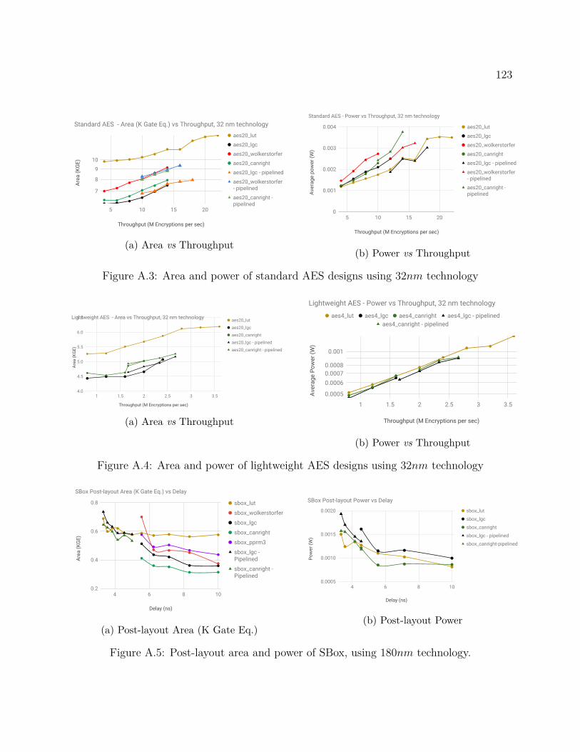
123
Throughput (M Encryptions per sec)
Area
(KG
E)
7
8
9
10
5 10 15 20
aes20_lut
aes20_lgc
aes20_wolkerstorfer
aes20_canright
aes20_lgc - pipelined
aes20_wolkerstorfer - pipelined
aes20_canright - pipelined
Standard AES - Area (K Gate Eq.) vs Throughput, 32 nm technology
(a) Area vs ThroughputThroughput (M Encryptions per sec)
Aver
age
pow
er (W
)
0
0.001
0.002
0.003
0.004
5 10 15 20
aes20_lut
aes20_lgc
aes20_wolkerstorfer
aes20_canright
aes20_lgc - pipelined
aes20_wolkerstorfer - pipelined
aes20_canright - pipelined
Standard AES - Power vs Throughput, 32 nm technology
(b) Power vs Throughput
Figure A.3: Area and power of standard AES designs using 32nm technology
Throughput (M Encryptions per sec)
Area
(KG
E)
4.0
4.5
5.0
5.5
6.0
6.5
1 1.5 2 2.5 3 3.5
aes20_lut
aes20_lgc
aes20_canright
aes20_lgc - pipelined
aes20_canright - pipelined
Lightweight AES - Area vs Throughput, 32 nm technology
(a) Area vs Throughput Throughput (M Encryptions per sec)
Aver
age
Pow
er (W
)
0.0005
0.00060.00070.0008
0.001
1 1.5 2 2.5 3 3.5
aes4_lut aes4_lgc aes4_canright aes4_lgc - pipelinedaes4_canright - pipelined
Lightweight AES - Power vs Throughput, 32 nm technology
(b) Power vs Throughput
Figure A.4: Area and power of lightweight AES designs using 32nm technology
Delay (ns)
Area
(KG
E)
0.2
0.4
0.6
0.8
4 6 8 10
sbox_lut
sbox_wolkerstorfer
sbox_lgc
sbox_canright
sbox_pprm3
sbox_lgc - Pipelined
sbox_canright - Pipelined
SBox Post-layout Area (K Gate Eq.) vs Delay
(a) Post-layout Area (K Gate Eq.)
Delay (ns)
Pow
er (W
)
0.0005
0.0010
0.0015
0.0020
4 6 8 10
sbox_lut
sbox_lgc
sbox_canright
sbox_lgc - pipelined
sbox_canright-pipelined
SBox Post-layout Power vs Delay
(b) Post-layout Power
Figure A.5: Post-layout area and power of SBox, using 180nm technology.

124 Appendix A. Additional results for logic synthesis of LGC circuits
Delay (ns)
Area
(KG
E)
0
1
2
3
4
4 6 8 10
polymult_mat, N=8
polymult_nist, N=8
polymult_comp, N=16
polymult_mat, N=16
polymult_nist, N=16
polymult_comp, N=22
polymult_mat, N=22
polymult_nist, N=22
Polynomial Multiplier Post-layout Area (K Gate Eq.) vs Delay
(a) Post-layout Area (K Gate Eq.)
Delay (ns)
Pow
er (W
)
0
0.002
0.004
0.006
0.008
4 6 8 10
polymult_mat, N=8
polymult_lgc, N=8
polymult_mat, N=16
polymult_lgc, N=16
polymult_mat, N=22
polymult_lgc, N=22
Poynomial Multiplier - Post-layout Power vs Delay
(b) Post-layout Power
Figure A.6: Post-layout area and power of Polynomial Multiplier, using 180nm technology.
Delay (ns)
Area
(KG
E)
0
0.5
1
1.5
4 5 6 7 8
gfmult_mastrovito, 2^8
gfmult_paar, 2^8
gfmult_lgc_tof, 2^8
gfmult_mastrovito, 2^16
gfmult_paar, 2^16
gfmult_lgc_tof, 2^16
GF Multiplier Post-layout Area (K Gate Eq.) vs Delay
(a) Post-layout Area (K Gate Eq.)
Delay (ns)
Pow
er (W
)
0.001
0.002
0.003
0.004
4 5 6 7
gfmult_paar gfmult_mastrovito gfmult_lgc
GF (2^16) Multiplier Post-layout Power vs Delay
(b) Post-layout Power
Figure A.7: Post-layout area and power of GF Multipliers, using 180nm technology.
Delay (ns)
Area
(KG
E)
0
0.2
0.4
0.6
4 6 8 10
gfinv_comp gfinv_rrb gfinv_lgc
GF(2^8) Inverter Post-layout Area (K Gate Eq.) vs Delay
(a) Post-layout Area - GF (28) Inverter
Delay (ns)
Area
(KG
E)
3
3.5
4
4.5
4 6 8 10
reedsolomon_ref reedsolomon_lgc
Reed-Solomon Encoder Post-layout Area (K Gate Eq.) vs Delay
(b) Post-layout Area - Reed-Solomon Encoder
Figure A.8: Post-layout area of GF (28) Inverter and Reed-Solomon Encoder.

125
Frequency (MHz)
Area
(KG
E)
15
20
25
30
35
100 125 150 175 200
aes20_lut aes20_lgc aes20_canrightaes20_lgc - pipelined aes20_canright - pipelined
Post-layout Area (K Gate Eq.) - Standard AES
(a) Post-layout Area (K Gate Eq.)
Frequency (MHz)
Pow
er (W
)
0
0.025
0.05
0.075
0.1
100 125 150 175 200
aes20_lut aes20_lgc aes20_canrightaes20_lgc - pipelined aes20_canright - pipelined
Post-layout Power - Standard AES
(b) Post-layout Power
Figure A.9: Post-layout area and power of standard AES, using 180nm technology.
Frequency (MHz)
Area
(KG
E)
15161718192021
100 125 150 175 200
aes4_lut aes4_lgc aes4_canrightaes4_lgc - pipelined aes4_canright - pipelined
Post-layout Area (K Gate Eq.) - Lightweight AES
(a) Post-layout Area (K Gate Eq.)
Frequency (MHz)
Pow
er (W
)
0.01
0.015
0.02
0.025
0.03
100 125 150 175 200
aes4_lut aes4_lgc aes4_canrightaes4_lgc - pipelined aes4_canright - pipelined
Post-layout Power - Lightweight AES
(b) Post-layout Power
Figure A.10: Post-layout area and power of lightweight AES, using 180nm technology.
Delay (ns)
Corr
elat
ion
-0.25
0
0.25
0.5
0.75
2.25 2.5 2.75 3 3.25 3.5 3.75
TSMC180 SAED32
GF Multipliers - Correlation between Area and Logical gate Count
(a) Logical Gate Count and Area
Delay (ns)
Corr
elat
ion
-0.25
0
0.25
0.5
0.75
2.5 3 3.5 4
TSMC180 SAED32
GF Multipliers - Correlation between Power and Logical gate Count
(b) Logical Gate Count and Power
Figure A.11: Correlation of logical gate count to hardware quality metrics of GF multipliers.
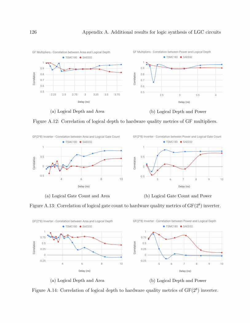
126 Appendix A. Additional results for logic synthesis of LGC circuits
Delay (ns)
Corr
elat
ion
0.5
0.6
0.7
0.8
0.9
1
2.25 2.5 2.75 3 3.25 3.5 3.75
TSMC180 SAED32
GF Multipliers - Correlation between Area and Logical Depth
(a) Logical Depth and Area
Delay (ns)
Corr
elat
ion
0.5
0.6
0.7
0.8
0.9
1
2.5 3 3.5 4
TSMC180 SAED32
GF Multipliers - Correlation between Power and Logical Depth
(b) Logical Depth and Power
Figure A.12: Correlation of logical depth to hardware quality metrics of GF multipliers.
Delay (ns)
Corr
elat
ion
-0.5
0
0.5
1
4 6 8 10
TSMC180 SAED32
GF(2^8) Inverter - Correlation between Area and Logical Gate Count
(a) Logical Gate Count and Area
Delay (ns)
Corr
elat
ion
-0.5
0
0.5
1
5 6 7 8 9 10
TSMC180 SAED32
GF(2^8) Inverter - Correlation between Power and Logical Gate Count
(b) Logical Gate Count and Power
Figure A.13: Correlation of logical gate count to hardware quality metrics of GF(28) inverter.
Delay (ns)
Corr
elat
ion
-0.25
0
0.25
0.5
0.75
1
4 6 8 10
TSMC180 SAED32
GF(2^8) Inverter - Correlation between Area and Logical Depth
(a) Logical Depth and Area
Delay (ns)
Corr
elat
ion
-0.25
0
0.25
0.5
0.75
1
5 6 7 8 9 10
TSMC180 SAED32
GF(2^8) Inverter - Correlation between Power and Logical Depth
(b) Logical Depth and Power
Figure A.14: Correlation of logical depth to hardware quality metrics of GF(28) inverter.

Appendix B
NISTCHIP Memory Map
Component AHB Address AHB Master / SlaveLeon3 Processor N/A MasterDMA Controller N/A MasterDebug UART N/A MasterBoot ROM 0x00000000 - 0x000FFFFF SlaveOn-Chip RAM 0x40000000 - 0x400FFFFF SlaveDebug Support Unit 0x90000000 - 0x9FFFFFFF Slave
0xFFF00200 - 0xFFF002FF (I/O part)SPI Memory Controller 0x10000000 - 0x10FFFFFF (Memory part) Slave
APB Controller 0 0x80000000 - 0x800FFFFF SlaveAPB Controller 1 0xA0000000 - 0xA00FFFFF SlaveAPB Controller 2 0xB0000000 - 0xB00FFFFF Slave
Table B.1: Address Map of components on AHB Bus
127

128 Appendix B. NISTCHIP Memory Map
Component APB Address BusUser UART 0x80000100 - 0x800001FF APB Bus 0Debug UART 0x80000300 - 0x800003FF APB Bus 0GPIO 0x80000500 - 0x800005FF APB Bus 0GP Timer 0x80000600 - 0x800006FF APB Bus 0Standalone EM Sensors 0xA0010000 - 0xA0010FFF APB Bus 1AES-LUT 0xA0020000 - 0xA0020FFF APB Bus 1Keymill 0xA0030000 - 0xA0030FFF APB Bus 1SBox with EM Sensors 0xA0040000 - 0xA0040FFF APB Bus 1ACORN (32-bit) 0xB0010000 - 0xB0010FFF APB Bus 2Reed-Solomon Encoder 0xB0020000 - 0xB0020FFF APB Bus 2NISTCOMB 0xB0030000 - 0xB0030FFF APB Bus 2AES-LGC 0xB0040000 - 0xB0040FFF APB Bus 2AES-WOLK 0xB0050000 - 0xB0050FFF APB Bus 2AEGIS 0xB0060000 - 0xB0060FFF APB Bus 2ACORN (8-bit) 0xB0070000 - 0xB0070FFF APB Bus 2MORUS 0xB0080000 - 0xB0080FFF APB Bus 2DMA Controller 0xB0090000 - 0xB0090FFF APB Bus 2
Table B.2: Address Map of components on APB Busses
Address Register R/W0 Control R/W
b0: Soft Resetb2,b1: Redundancyb3: GF Modeb7-b4: Function
1 Input0 R/W2 Input1 R/W3 Input2 R/W4 Input3 R/W5 Output0 R6 Output1 R7 Output2 R8 Output3 R
Table B.3: NISTCOMB software-interface
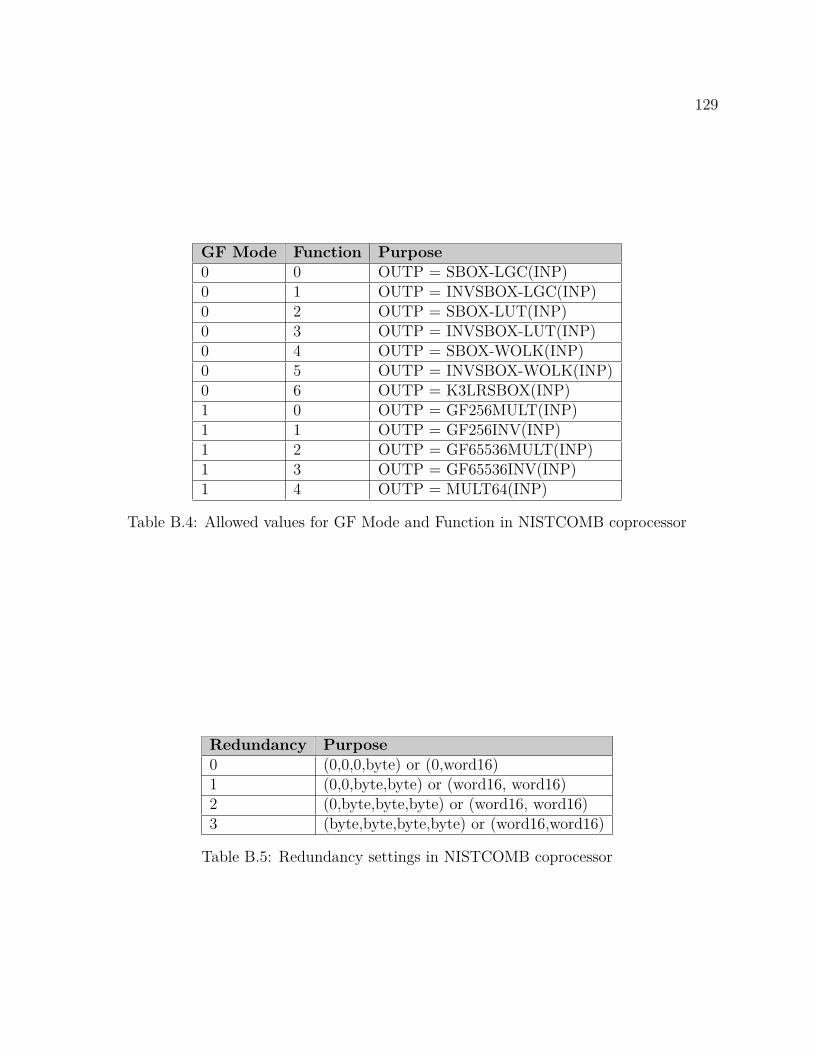
129
GF Mode Function Purpose0 0 OUTP = SBOX-LGC(INP)0 1 OUTP = INVSBOX-LGC(INP)0 2 OUTP = SBOX-LUT(INP)0 3 OUTP = INVSBOX-LUT(INP)0 4 OUTP = SBOX-WOLK(INP)0 5 OUTP = INVSBOX-WOLK(INP)0 6 OUTP = K3LRSBOX(INP)1 0 OUTP = GF256MULT(INP)1 1 OUTP = GF256INV(INP)1 2 OUTP = GF65536MULT(INP)1 3 OUTP = GF65536INV(INP)1 4 OUTP = MULT64(INP)
Table B.4: Allowed values for GF Mode and Function in NISTCOMB coprocessor
Redundancy Purpose0 (0,0,0,byte) or (0,word16)1 (0,0,byte,byte) or (word16, word16)2 (0,byte,byte,byte) or (word16, word16)3 (byte,byte,byte,byte) or (word16,word16)
Table B.5: Redundancy settings in NISTCOMB coprocessor

Appendix C
Additional results for SoC integration
of AEAD Ciphers
Component on Chip % of Total powerOn-Chip Memory 27.92%Processor 7.82%AEGIS Coprocessor 12.6%DMA Controller 5.02%Cache controller 0.8%AHB 0.3%APB 0.3%
Table C.1: AEGIS-128L Tests - Power split
Block Clock Network powerTop-level 55.86%Processor 65.83%AEGIS Coprocessor
With FIFOs 77.06%Without FIFOs 66.3%
DMA Controller 21.27%Cache controller 32.02%
Table C.2: AEGIS-128L Tests - Clock power
Ener
gy p
er B
it (n
J/bi
t)
3
3.5
4
4.5
5
5.5
2 FIFOs, no DMA
Output FIFO, no DMA
No FIFO 2 FIFOs, DMA Output FIFO, DMA
Top-level Energy-per-bit - AEGIS-128L Test, Small messages
(a) Top-level
Eerg
y pe
r Bit
(nJ/
bit)
0.00E+00
2.00E-01
4.00E-01
6.00E-01
8.00E-01
Processor AEGIS Coprocessor
AEGIS-FIFO AEGIS-Core DMA
2 FIFOs, no DMA Output FIFO, no DMA No FIFO 2 FIFOs, DMAOutput FIFO, DMA
Block-level Energy-per-bit - AEGIS-128L Test, Small messages
(b) Block-level
Figure C.1: Energy efficiency of AEGIS coprocessor alternatives, for small messages.
130

131En
ergy
-per
-bit
(nJ/
bit)
4.00E+00
4.50E+00
5.00E+00
5.50E+00
6.00E+00
6.50E+00
2 FIFOs, no DMA
Output FIFO, no DMA
No FIFO 2 FIFOs, DMA
Output FIFO, DMA
Top-level Energy-per-Bit - MORUS-1280 Test, Small messages
(a) Top-levelEn
ergy
-per
-bit
(nJ/
bit)
0.00E+00
2.00E-01
4.00E-01
6.00E-01
Processor MORUS- Coprocessor
MORUS-FIFO MORUS-Core DMA
2 FIFOs, no DMA Output FIFO, no DMA No FIFO 2 FIFOs, DMAOutput FIFO, DMA
Block-level Energy-per-Bit - MORUS-1280 Test, Small messages
(b) Block-level
Figure C.2: Energy efficiency of MORUS coprocessor alternatives, for small messages.
Ener
gy-p
er-b
it (n
J/bi
t)
1.40E+01
1.60E+01
1.80E+01
2.00E+01
2.20E+01
2.40E+01
2.60E+01
Two FIFOs, no DMA Two FIFOs, DMA
Top-level Energy-per-bit - ACORN-8 Test, Small messages
(a) Top-level
Ener
gy-p
er-b
it (n
J/bi
t)
0.00E+00
5.00E-01
1.00E+00
1.50E+00
2.00E+00
2.50E+00
Processor ACORN-8 Coprocessor
ACORN-8 FIFO
ACORN-8 Core
DMA
Two FIFOs, no DMA Two FIFOs, DMA
Block-level Energy-per-bit - ACORN-8 Test, Small messages
(b) Block-level
Figure C.3: Energy efficiency of ACORN-8 coprocessor alternatives, for small messages.