eecs 427eecs 427 vlsi design i · eecs 427eecs 427 vlsi design i ... – the entire process of very...
TRANSCRIPT

1
EECS 427EECS 427VLSI Design I
TuTh 10:00-11:30am Disc: Tu 5:30-6:30pm
EECS 427 F08 Lecture 1 1
pProf. David Blaauw
http://www.eecs.umich.edu/courses/eecs427
Outline
• What you can expect to learn in this class• What you can expect to learn in this class• Logistics – teaching staff intro, go over
syllabus• CMOS processing sequence
EECS 427 F08 Lecture 1 2

2
What you will learn in 427• 312 – Transistors design and behavior• 270 – Logic design – combining transistorsg g g• 370 – Architecture – high level organization
• 427 – VLSI: realization of circuits in silicon: – The entire process of very large-scale integration– Generation of custom layout– Sub-system design such as adders, register files..
EECS 427 F08 Lecture 1 3
y g g– Synthesis + automated place/route design flow– Advanced circuit design topics: pulsed latches,
memory decoder and sense amplifiers, power, etc.Project - Teamwork
Teaching Staff• Primary instructors:
– David Blaauwoffice hours: Tuesday 11:30 1:00pm Thursday 11:30• office hours: Tuesday 11:30 – 1:00pm, Thursday 11:30 –Noon. Both lecture material and project
• GSI:– Brian Cline
• Support of CAD (Computer-Aided Design) tools and project related issues as well as lecture material.
• Staff support:
EECS 427 F08 Lecture 1 4
• Staff support:– Joel Van Laven
• Major CAD tool issues (pertaining to the project); consult after Brian

3
Course setup
• Tues and Thur lectures in 1303 EECS• Tuesday discussion section led by Brian (1200 EECS)uesday d scuss o sec o ed by a ( 00 CS)
– Purpose of discussion: review lecture topics, review CAD assignments and answer project related questions
• Homeworks– Only 1 ‘typical’ HW, others handle planning issues of project
(groups, initial proposal, etc.)• CAD assignments
– Roughly weekly, several 2+week assignmentsE h i t t t f fi l
EECS 427 F08 Lecture 1 5
– Each assignment represents a component of your final microprocessor design
– First 2 are individual, rest are in groups• Quizzes: 2 - roughly every 6 weeks, non-cumulative.
Project• Main component of class, 70+% of your grade• Design a 16-bit RISC (reduced instruction set
computing) processorcomputing) processor– Groups of 4 (you choose)
• Good to have a mix of EE and CE • Baseline architecture (instruction set) given to you; you choose
and implement a circuit-level enhancement technique– Time requirements: 30-40 hrs/week avg. 427 → 247– Peer contribution forms; must pull your weight
• Learn full-custom design (datapath) and automation tools (logic synthesis + custom router + place/route)
EECS 427 F08 Lecture 1 6
tools (logic synthesis + custom router + place/route)• You can send this design off to be fabricated and
then test it later as a directed study or possibly in EECS 579 (encouraged!)

4
Logistics• Course Textbook:
Digital Integrated Circuits: A Design Perspective, 2nd
edition by Rabaey Chandrakasan and Nikolicedition by Rabaey, Chandrakasan, and Nikolic
• Lecture notes will be posted online shortly after class sessions and I will bring copies to class for note taking
• Book will be supplemented with several handouts from other sources throughout the semesterOth b k t M di U i (W t
EECS 427 F08 Lecture 1 7
• Other books on reserve at Media Union (Weste, Chandrakasan)– Weste/Harris in particular is recommended if you want to
pursue a career/graduate studies in digital circuits
Grade Breakdown
• Your project, in the form of CAD assignments and final report/presentation is the dominantand final report/presentation, is the dominant part of your grade
Homework 10%CAD assignments 35%Quizzes 24% (12% each)
EECS 427 F08 Lecture 1 8
( )Final project/report, indiv. contrib. 31%
CAD late policy: within 24 hours = 25% penalty, 24-48 hours = 50% penalty, see course info handout

5
Project Schedule• Tutorial 1 (CAD): Tuesday, September 2 - 5:30 – 7:30• CAD1 (Inverter/Nand/Mux): Monday, September 8• CAD2 (D flip-flop): Monday September 15• CAD2 (D flip-flop): Monday, September 15• CAD3 (Register file): Friday, September 26• CAD4 (ALU): Friday, October 10• CAD5 (Shifter): Friday, October 24• Tutorial 2 (verilog): Tuesday, October 28• CAD6 (Datapath): Friday, October 31• CAD7 (program counter): Friday, November 7
EECS 427 F08 Lecture 1 9
(p g ) y,• CAD8 (controller): Friday, November 14• CAD9 (completion):
– Presentation & demo: Thursday Dec 12, – Report due: Same day (Dec. 12) at 7am
Lecture ScheduleDate Topic Reading/Coverage Notes,
assignments dueSeptember 2 Course Introduction, 1.1-1.3 (review), 2.2, CAD tutorial, 9/2
Manufacturing WH 3.2 5:30-7:30pm & 7:30-9:30, 1695 CSE
9/4 Design Rules & Layout 2.3, Insert A, WH 1.5, WH 3.3
CAD1 due 9/8
9/9 Design Styles Overview 8.1-8.4
9/11 CMOS Review 5.4, 6.2 HW1 due in classCAD2 due 9/15
9/16 Interconnect Review 4.3.1, 4.3.2, 4.4.1-4.4.3, 9.3.3
HW2 due in class (teams)
9/18 Project Architecture and Intro to Logical Effort
handouts
9/23 Logical Effort handouts
9/25 Adders 11.1-11.3.1 CAD3 due 9/26
9/30 Adders 11.3.2-11.3.3
EECS 427 F08 Lecture 1 10

6
Lecture ScheduleDate Topic Reading/Coverage Notes,
assignments dueOctober 2 Shifters 11.5, WH 10.8 HW3 due in class
(initial proposal)10/7 Multipliers 11.4
10/9 Power/Energy, Dynamic Logic
5.5, 6.3, CBF 7 CAD4 due 10/10
10/14 Low-Power ALUs 11.7
10/16 Quiz 1
10/20, 10/21 - Fall Study Break, No Classes
10/23 Counters pipelining WH 10 5 notes CAD5 due 10/2410/23 Counters, pipelining WH 10.5, notes CAD5 due 10/24
10/28 Synthesis/APR flow Notes, WH 8.4
10/30 Timing, skew/jitter 10.1-10.3 CAD6 due 10/31
November 4 Timing cont., D-Q, pulsed latches
10.3, 7.4 HW4 due in class (detailed proposal)
EECS 427 F08 Lecture 1 11
Lecture ScheduleDate Topic Reading/Coverage Notes,
assignments due11/6 Design-for-Test (DFT) Insert H.3, CBF 25 CAD7 due 11/7
11/11 Memory Core and Peripherals
12.1-12.3
11/13 Memory Reliability and Power 12.4, 12.5 CAD8 due 11/14
11/18 System-Level Power Reduction
6.4.2, CBF 4
11/20 Quiz 2
11/25 Clock Distribution & Robustness
10.3.3, 10.6,CBF Ch. 13
11/26, 11/27, 11/28 - Thanksgiving Break, No Classes
EECS 427 F08 Lecture 1 12

7
Lecture ScheduleDate Topic Reading/Coverage Notes,
assignments dueDecember 2 Advanced Interconnect 9.5
Techniques12/4 Power Grid and Other Issues WH 12.3, CBF 24
12/9 Process Variation Course Evaluations in class
12/12 Final Project DemosFinal Project Presentations(Time TBD)
CAD9: Final DueHW5: Final Report due @7amHW6: Presentations
EECS 427 F08 Lecture 1 13
5 Minute break!
EECS 427 F08 Lecture 1 14

8
CMOS Process
EECS 427 F08 Lecture 1 15
A Modern CMOS Process
gate-oxide
p-well n-well
p-epi
SiO2
AlCu
poly
n+
SiO2
p+
Tungsten
TiSi2
EECS 427 F08 Lecture 1 16
p+
DualDual--Well TrenchWell Trench--Isolated CMOS ProcessIsolated CMOS Process
9
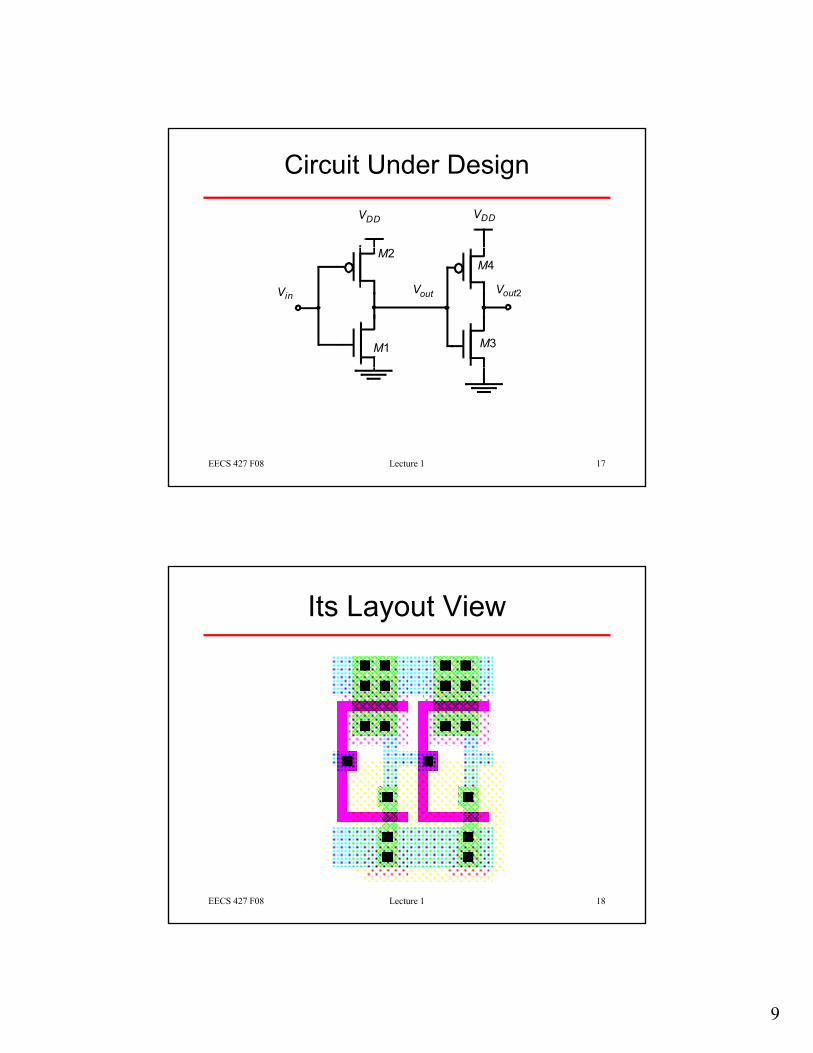
Circuit Under Design
VDD VDD
Vin Vout
M1
M2
M3
M4
Vout2
EECS 427 F08 Lecture 1 17
Its Layout View
EECS 427 F08 Lecture 1 18

10
oxidation
opticalmask
Photolithographic Process
photoresist coatingphotoresistremoval (ashing)
photoresist
stepper exposure
development
Typical operations in a single photolithographic cycle (from [Fullman]).
EECS 427 F08 Lecture 1 19
processstep
spin, rinse, dryacid etch
development
Patterning of SiO2
Si-substrate
(a) Silicon base materialSiO2Hardened resist
Chemical or plasmaetch
(a) Silicon base material
(b) After oxidation and depositionof negative photoresist
PhotoresistSiO2
UV-lightPatterned
Si-substrate
Si-substrate
Si-substrate
SiO2
(d) After development and etching of resist,chemical or plasma etch of SiO2
(e) After etching
Hardened resist
EECS 427 F08 Lecture 1 20
Si-substrate Si-substrate
(c) Stepper exposure
optical mask
Exposed resist SiO2
(e) te etc g
(f) Final result after removal of resist

11
CMOS Process at a GlanceDefine active areasEtch and fill trenches
Implant well regions
Deposit and patternpolysilicon layer
Implant source and drain
EECS 427 F08 Lecture 1 21
Implant source and drainregions and substrate contacts
Create contact and via windowsDeposit and pattern metal layers
CMOS Process Walkthrough
p-epi (a) Base material: p+ substrate with p-epi layerp+ with p-epi layer
p+
p-epi SiO2
3SiN
4(b) After deposition of gate-oxide and sacrificial nitride (acts as abuffer layer)
EECS 427 F08 Lecture 1 22
p+
(c) After plasma etch of insulatingtrenches using the inverse of the active area mask

12
CMOS Process WalkthroughSiO2
(d) After trench filling,CMP planarization and
n
CMP planarization, and removal of sacrificial nitride
(e) After n-well and Vthpadjust implants
EECS 427 F08 Lecture 1 23
p(e) After p-well and Vthnadjust implants
CMOS Process Walkthroughpoly(silicon)
(g) After polysilicon deposition
p+n+
(g) After polysilicon depositionand etch
(h) After n+ source/drain andp+ source/drain implants. Thesesteps also dope poly.
EECS 427 F08 Lecture 1 24
SiO2
(i) After deposition ofSiO2 insulator and contacthole etch

13
CMOS Process Walkthrough
Al
AlSiO2
(j) After deposition andpatterning of first Al layer.
EECS 427 F08 Lecture 1 25
(e) After deposition of SiO2Insulator, etching of vias, deposition and patterning of2nd layer of Al
Looking Ahead• http://jas.eng.buffalo.edu/education/fab/invFab/index.html• Read Sections 1.1, 1.2, 1.3.2-1.3.4, and 2.2 , , ,
of Rabaey (mostly review)• Next lecture: we’ll cover design rules and
layout styles
EECS 427 F08 Lecture 1 26