eb65 - ispmach 4256ze breakout board evaluation kit user's guide
TRANSCRIPT
March 2012Revision: EB65_01.1
ispMACH 4256ZE Breakout Board Evaluation Kit
User’s Guide

2
ispMACH 4256ZE Breakout Board Evaluation Kit User’s Guide
IntroductionThank you for choosing the Lattice Semiconductor ispMACH® 4256ZE Breakout Board Evaluation Kit!
This user’s guide describes how to start using the ispMACH 4256ZE Breakout Board, an easy-to-use platform for evaluating and designing with the ispMACH 4256ZE CPLD. Along with the board and accessories, this kit includes a pre-loaded hardware test program. You may also reprogram the on-board ispMACH 4256ZE device to review your own custom designs.
Note: Static electricity can severely shorten the lifespan of electronic components. See the Storage and Handlingsection for handling and storage tips.
FeaturesThe ispMACH 4256ZE Breakout Board Evaluation Kit includes:
• ispMACH 4000ZE Breakout Board – The board is a 3” x 3” form factor that features the following on-board components and circuits:
– ispMACH 4256ZE CPLD (LC4256ZE-5TN144C)– USB mini-B connector for power and programming– Eight LEDs– 4x15 prototype area– Four 2x20 expansion header landings for general I/O, JTAG, and external power– 1x8 expansion header landing for JTAG – 3.3V and 1.8V supply rails
• Pre-loaded Demo – The kit includes a pre-loaded counter design that highlights use of the embedded ispMACH 4000ZE oscillator and programmable I/Os configured for LED drive.
• USB Connector Cable – The board is powered from the USB mini-B socket when connected to a host PC. The USB channel also provides a programming interface to the ispMACH 4256ZE JTAG port.
• Lattice Breakout Board Evaluation Kits Web Page – Visit www.latticesemi.com/breakoutboards for the latest documentation (including this guide), demo designs, and drivers for the kit.
The content of this user’s guide includes demo operation, programming instructions, top-level functional descrip-tions of the Breakout board, descriptions of the on-board connectors, and a complete set of schematics.
3
ispMACH 4256ZE Breakout Board Evaluation Kit User’s Guide
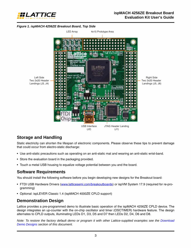
Figure 1. ispMACH 4256ZE Breakout Board, Top Side
Left SideTwo 2x20 HeaderLandings (J3, J4)
LED Array 4x15 Prototype Area
Right SideTwo 2x20 Header Landings (J5, J6)
USB Interface(J2)
JTAG Header Landing(J1)
Storage and HandlingStatic electricity can shorten the lifespan of electronic components. Please observe these tips to prevent damage that could occur from electro-static discharge:
• Use anti-static precautions such as operating on an anti-static mat and wearing an anti-static wrist-band.
• Store the evaluation board in the packaging provided.
• Touch a metal USB housing to equalize voltage potential between you and the board.
Software RequirementsYou should install the following software before you begin developing new designs for the Breakout board:
• FTDI USB Hardware Drivers (www.latticesemi.com/breakoutboards) or ispVM System 17.9 (required for re-pro-gramming)
• Optional: ispLEVER Classic 1.4 (ispMACH 4000ZE CPLD support)
Demonstration DesignLattice provides a pre-programmed demo to illustrate basic operation of the ispMACH 4256ZE CPLD device. The design integrates an up-counter with the on-chip oscillator and timer (OSCTIMER) hardware feature. The design alternates to CPLD outputs, illuminating LEDs D1, D3, D5 and D7 then LEDs D2, D4, D6 and D8.
Note: To restore the factory default demo or program it with other Lattice-supplied examples see the Download Demo Designs section of this document.

4
ispMACH 4256ZE Breakout Board Evaluation Kit User’s Guide
The preprogrammed demonstration design is an up counter and an output multiplexer to drive an LED array. The demo shows a clock generator based on the ispMACH 4256ZE on-chip oscillator and timer (OSCTIMER) hardware feature. The counter module is clocked at <5kHz to illustrate the ease at which very low speed timer functions can be implemented with a CPLD. The 15-bit up counter advances each second. An output mux selects between hexa-decimal patterns AAh or 55h depending on the count. The resulting light pattern will appear as an alternating pair of lit LEDs per row.
Figure 2. Counter Demo Block Diagram
2x4 LED Array
ispMACH 4256ZE
15-bitUp Counter
ClockGenerator < 5kHz
AAh
55h
0: Count < 2 1: Count >= 2
0
1
Run the Demonstration DesignWARNING: Do not connect the Breakout Board to your PC before you follow the driver installation procedure of this section.
Communication with the Breakout Board with a PC via the USB connection cable will require the FTDI chip USB hardware drivers contained in the Software Requirements section. Loading these drivers enables the computer to reliably recognize and program the Breakout Board. Drivers are distributed by Lattice as a stand-alone package or with ispVM System version 17.9 or later. Use one of the two procedures below to install.
To load the FTDI chip USB hardware drivers via ispVM System:
1. Browse to www.latticesemi.com/breakoutboards and download ispVM System software.
2. Install ispVM System software.
3. Run ispVM System. Choose ispTools > Install/Uninstall LSC USB/Parallel Port Driver.The LSC 32/64-Bit USB Drivers Install/Uninstall dialog appears.
4. Select FTDI USB 32-Bit Driver or FTDI USB 64-Bit Driver then click Install.After a few moments, ispVM will indicate the installation is complete.
5. Click OK, then click Close from the LSC 32/64-Bit USB Drivers Install/Uninstall dialog.
6. Choose File > Exit to close ispVM System.
7. Connect the USB cable from a USB port on your PC to the board’s USB mini-B socket (J2). After connection is made, a green Power LED (D9) will light indicating the board is powered on.
8. Red LEDs will light and start to flash according to the preprogrammed demonstration design.
See the Troubleshooting section of this guide if the board does not function as expected.

5
ispMACH 4256ZE Breakout Board Evaluation Kit User’s Guide
To load the FTDI chip USB hardware drivers via the stand-alone package:
1. Browse to www.latticesemi.com/breakoutboards and download the FTDI chip USB Hardware driver package.
2. Extract the FTDI chip USB Hardware driver package to your PC hard drive.
3. Connect the USB cable from a USB port on your PC to the board’s USB mini-B socket (J2). After connection is made, a green Power LED (D9) will light indicating the board is powered on.
4. If you are prompted, “Windows may connect to Windows Update” select No, not this time from available options and click Next to proceed with the installation. Choose the Install from specific location (Advanced) option and click Next.
5. Search for the best driver in these locations and click the Browse button to browse to the Windows driver folder created in the Download Windows USB Hardware Drivers section. Select the CDM 2.04.06 WHQL Certified folder and click OK.
6. Click Next. A screen will display as Windows copies the required driver files. Windows will display a message indicating that the installation was successful.
7. Click Finish to install the USB driver.
8. Red LEDs will light and start to flash according to the preprogrammed demonstration design.
See the Troubleshooting section of this guide if the board does not function as expected.
Download Demo DesignsA demo is preprogrammed into the Breakout Board, however over time it is likely your board will be modified. Lat-tice distributes source and programming files for demonstration designs compatible with the Breakout Board.
To download demo designs:
1. Browse to the Lattice Breakout Board web page (www.latticesemi.com/breakoutboards). Select the ispMACH 4256ZE Demo Application download and save the file.
2. Extract the contents of ispMACH4256ZE_BB_Eval_Kit_v01.0.zip to an accessible location on your hard drive.
The demo design directory, LC4256ZE_CTL, is unpacked.
Recompile a Demonstration Project with ispLEVER ClassicUse the procedure described below to recompile a demo project for the Breakout Board.
1. Install and license ispLEVER Classic software.
2. Run the ispLEVER Classic Project Navigator.
3. Browse to the demo design directory, LC4256ZE_CTL, and open the LC4256ZE.syn project file.
4. From the Source in project window, select the target device. The Fit Design process appears in the Processes for current source window.
5. Select Fit Design, right-click and choose Start.After a few moments the JEDEC programming file is output.
6. See the Programming with ispVM section for details on downloading a programming file to the board.

6
ispMACH 4256ZE Breakout Board Evaluation Kit User’s Guide
Programming with ispVMA demonstration design is pre-programmed into the Breakout Board by Lattice. To restore a Breakout Board to fac-tory settings or load an alternative demo design, use the procedures in this section.
To install ispVM programming tools:
1. Install and license ispVM System software.
2. Connect the board to a host PC using the USB port header connection.
3. Follow the USB Cable Interface procedure below to program the evaluation board.
The Breakout Board is equipped with a built-in USB-based programming circuit. This consists of a USB PHY and a USB connector. When the board is connected to a PC with a USB cable, it is recognized by the ispVM System soft-ware as a USB Download Cable. The ispMACH 4256ZE can then be scanned and programmed using the ispVM System software.
To program a demo programming file:
1. From the Start menu run ispVM System.ispVM appears.
2. Choose Options > Cable and IO Port Setup…The Cable and I/O Port Setup dialog appears.
3. Make the following selections:
Cable Type: USB2Port Setting: FTUSB-0
Click OK.
4. Choose ispTools > Scan Chain.The New Scan Configuration Setup window appears. The LC4256ZE device appears in the device list.
5. Right-click the LC4256ZE entry and choose Edit Device…The Device Information dialog appears.
6. From the Data File section, click the Browse button.The Open Data File dialog appears.
7. Browse to the <Demo Dir> folder, select <Demo>.jed, and click Open. From the Operation list choose Erase, Program, Verify and click OK.
8. Choose Project > Download.ispVM reprograms the evaluation board.
Programming requires about 10 seconds. A small timer window will appear to show elapsed programming time. At the end of programming, the configuration setup window should show a “PASS” in the Status column.
ispMACH 4256ZE Breakout BoardThis section describes the features of the ispMACH 4256ZE Breakout board in detail.
OverviewThe ispMACH 4256ZE Breakout Board is a complete development platform for the ispMACH 4256ZE CPLD. The board includes a prototyping area, a USB program/power port, an LED array, and header landings with electrical connections to most of the CPLDs programmable I/O, power and JTAG pins. The board is powered by the PC’s
7
ispMACH 4256ZE Breakout Board Evaluation Kit User’s Guide
USB port or optionally with external power. You may create or modify CPLD program files using ispLEVER Classic software and reprogram the board using ispVM software.
Figure 3. ispMACH 4000ZE Breakout Board Block Diagram
ispMACH4256ZE-5TN144C
2x20 Header Landing (J3)
LEDArray
20 GPIO
USBController
USB Mini B Socket
A/Mini-BUSB Cable JTAG
Programming 8
2x20 Header Landing (J4)
35 GPIO
2x20 Header Landing (J5)
40 GPIO
2x20 Header Landing (J6)
15 GPIO
1x8 JTAG Header Landing (J1)
8
Table 1 describes the components on the board and the interfaces it supports.
Table 1. Breakout Board Components and Interfaces
Component/Interface Type Schematic Reference Description
Circuits
USB Controller Circuit U2: FT2232H USB-to-JTAG interface and dual USB UART/FIFO IC
USB Mini-B Socket I/O J1:USB_MINI_B Programming and debug interface
Components
LC4256ZE CPLD U4: LC4256ZE-5TN144C 256-macrocell CPLD packaged in a 20 x 20mm, 144-pin TQFP
Interfaces
LED Array Output D8-D1 Red LEDs
Four 2x20 header landings I/O
J3: header_2x20J4: header_2x20J5: header_2x20J6: header_2x20
User-definable I/O
1x8 header landing I/O J1: header_1x8 Optional JTAG interface
4x15 prototype area J9 Prototype area 100mil centered holes
SubsystemsThis section describes the principle subsystems for the ispMACH 4256ZE Breakout Board in alphabetical order.
Clock SourcesAll clocks for the counter demonstration designs originate from the ispMACH 4256ZE CPLD on-chip oscillator and timer (OSCTIMER) block. You may use an expansion header landing to drive a CPLD input with an external clock source.
Expansion Header LandingsThe expansion header landings provide access to user GPIOs, primary inputs, clocks, and Bank 0/1 VCCO pins of the ispMACH 4256ZE. The remaining pins serve as power supplies for external connections. Each landing is con-figured as one 2x20 100 mil.
Table 2. Expansion Connector Reference
Item Description
Reference Designators J3, J4, J5, J6
Part Number header_2x20
8
ispMACH 4256ZE Breakout Board Evaluation Kit User’s Guide
Table 3. Expansion Header Pin Information (J3)
Pin Number Function LC4256ZE Pin
1 IO_C12 4
2 GND n/a
3 IO_C10 5
4 GND n/a
5 IO_C8 6
6 GND n/a
7 IO_C6 7
8 GND n/a
9 IO_C4 8
10 GND n/a
11 IO_C2 9
12 GND n/a
13 IO_D14 11
14 GND n/a
15 IO_D12 12
16 GND n/a
17 IO_D10 13
18 GND n/a
19 IO_D8 14
20 GND n/a
21 IO_D6 15
22 GND n/a
23 IO_D4 16
24 GND n/a
25 IO_IA1 17IN
26 GND n/a
27 IO_IA2 20IN
28 GND n/a
29 IO_E2 21
30 GND n/a
31 IO_E4 22
32 GND n/a
33 IO_E6 23
34 GND n/a
35 IO_E8 24
36 GND n/a
37 IO_E10 25
38 GND n/a
39 IO_E12 26
40 GND n/a
9
ispMACH 4256ZE Breakout Board Evaluation Kit User’s Guide
Table 4. Expansion Header Pin Information (J4)
Pin Number Function LC4256ZE Pin
1 IO_F2 28
2 IO_A2 130
3 IO_F4 29
4 IO_A4 131
5 IO_F6 30
6 IO_A6 132
7 IO_F8 31
8 IO_A8 133
9 IO_F10 32
10 IO_A10 134
11 IO_F12 33
12 IO_A12 135
13 IO_G12 39
14 IO_B2 138
15 IO_G10 40
16 IO_B4 139
17 IO_G8 41
18 IO_B6 140
19 IO_G6 42
20 IO_B8 141
21 IO_G4 43
22 IO_B10 142
23 IO_G2 44
24 IO_B12 143
25 IO_IA3 38IN
26 IO_IA5 144IN
27 IO_IA4 45IN
28 GND n/a
29 IO_H12 48
30 NC n/a
31 IO_H10 49
32 GND n/a
33 IO_H8 50
34 CLK1 54CLK
35 IO_H6 51
36 GND n/a
37 IO_H4 52
38 CLK0 128CLK
39 IO_H2 53
40 GND n/a

10
ispMACH 4256ZE Breakout Board Evaluation Kit User’s Guide
Table 5. Expansion Header Pin Information (J5)
Pin Number Function LC4256ZE Pin
1 IO_P2 125
2 IO_M12 98
3 IO_P4 124
4 IO_M10 97
5 IO_P6 123
6 IO_M8 96
7 IO_P8 122
8 IO_M6 95
9 IO_P10 121
10 IO_M4 94
11 IO_P12 120
12 IO_M2 93
13 IO_IB10 117IN
14 IO_IB8 92IN
15 IO_IB9 110IN
16 IO_IB7 89IN
17 IO_O2 116
18 IO_L4 88
19 IO_O4 115
20 IO_L6 87
21 IO_O6 114
22 IO_L8 86
23 IO_O8 113
24 IO_L10 85
25 IO_O10 112
26 IO_L12 84
27 IO_O12 111
28 IO_L14 83
29 IO_N12 105
30 IO_K2 81
31 IO_N10 104
32 IO_K4 80
33 IO_N8 103
34 IO_K6 79
35 IO_N6 102
36 IO_K8 78
37 IO_N4 101
38 IO_K10 77
39 IO_N2 100
40 IO_K12 76
11
ispMACH 4256ZE Breakout Board Evaluation Kit User’s Guide
Table 6. Expansion Header Pin Information (J6)
Pin Number Function LC4256ZE Pin
1 VCC_3.3V VCCO_33
2 GND GND
3 VCC_3.3V VCCO_33
4 GND GND
5 VCC_3.3V VCCO_33
6 GND GND
7 NC NC
8 GND GND
9 NC NC
10 V_ext_1_8v VCC_EXT
11 GND GND
12 GND GND
13 IO_J2 66
14 V_ext_B0 VCCO_EXT_0
15 IO_J4 67
16 V_ext_B1 VCCO_EXT_1
17 IO_J6 68
18 GND GND
19 IO_J8 69
20 NC NC
21 IO_J10 70
22 NC NC
23 IO_J12 71
24 NC NC
25 IO_IB6 72IN
26 NC NC
27 GND GND
28 NC NC
29 IO_I2 58
30 NC NC
31 IO_I4 59
32 GND GND
33 IO_I6 60
34 CLK3 126CLK
35 IO_I8 61
36 GND GND
37 IO_I10 62
38 CLK2 56CLK
39 IO_I12 63
40 GND GND
12
ispMACH 4256ZE Breakout Board Evaluation Kit User’s Guide
Figure 4. J3/J4 Header Landing Callout
J3 J4
4 GND 5 GND 6 GND 7 GND 8 GND 9 GND 11 GND 12 GND 13 GND 14 GND 15 GND 16 GND
17 IN GND 20 IN GND
21 GND 22 GND 23 GND 24 GND 25 GND 26 GND
J3
28 130 29 131 30 132 31 133 32 134 33 135 39 138 40 139 41 140 42 141 43 142 44 143
38 IN 144 IN 45 IN GND
48 NC 49 GND 50 54 CLK 51 GND 52 128 CLK 53 GND
J4
1 2 1 2
39 40 39 40
Top Side
Figure 5. J5/J6 Header Landing Callout
J5 J6
1 2 1 2
39 40 39 40
J5 J6
VCCO_33 GND
VCCO_33 GND
VCCO_33 GND
NC GND
NC VCC_EXT
GND GND
66 VCCO_EXT_0
67 VCCO_EXT_1
68 GND
69 NC
70 NC
71 NC
72 IN NC
GND NC
58 NC
59 GND
60 56 CLK
61 GND
62 126 CLK
63 GND
125 98
124 97
123 96
122 95
121 94
120 93
117 IN 92 IN
110 IN 89 IN
116 88
115 87
114 86
113 85
112 84
111 83
105 81
104 80
103 79
102 78
101 77
100 76
Top Side

13
ispMACH 4256ZE Breakout Board Evaluation Kit User’s Guide
Figure 6. J1 Header Landing and LED Array Callout
J1
1
J1
VCC3FT
NC
NC
35 (TCK)
2 (TDI)
107 (TDO)
74 (TMS)
GND
Top Side
58 59 60 61 62 63 70 71
LED
D1D5
8
D4D8
ispMACH4256ZE-TN144 CPLDThe board features the ispMACH 4000ZE CPLD which is ideal for low-power, high-volume portable applications. The on-board ispMACH 4256ZE is the highest capacity device of the family with 256 macrocells (equivalent to about 450 FPGA LUTs). The 144-pin TQFP package provides 96 user I/Os and 4 dedicated inputs in a 20mm x 20mm package. The ispMACH 4256ZE consumes standby current as low as 15µA. A complete description of this device can be found in the ispMACH 4000ZE Family Data Sheet.
Table 7. ispMACH 4256ZE CPLD Interface Reference
Item Description
Reference Designator U4
Part Number LC4256ZE-5TN144C
Manufacturer Lattice Semiconductor
Web Site www.latticesemi.com
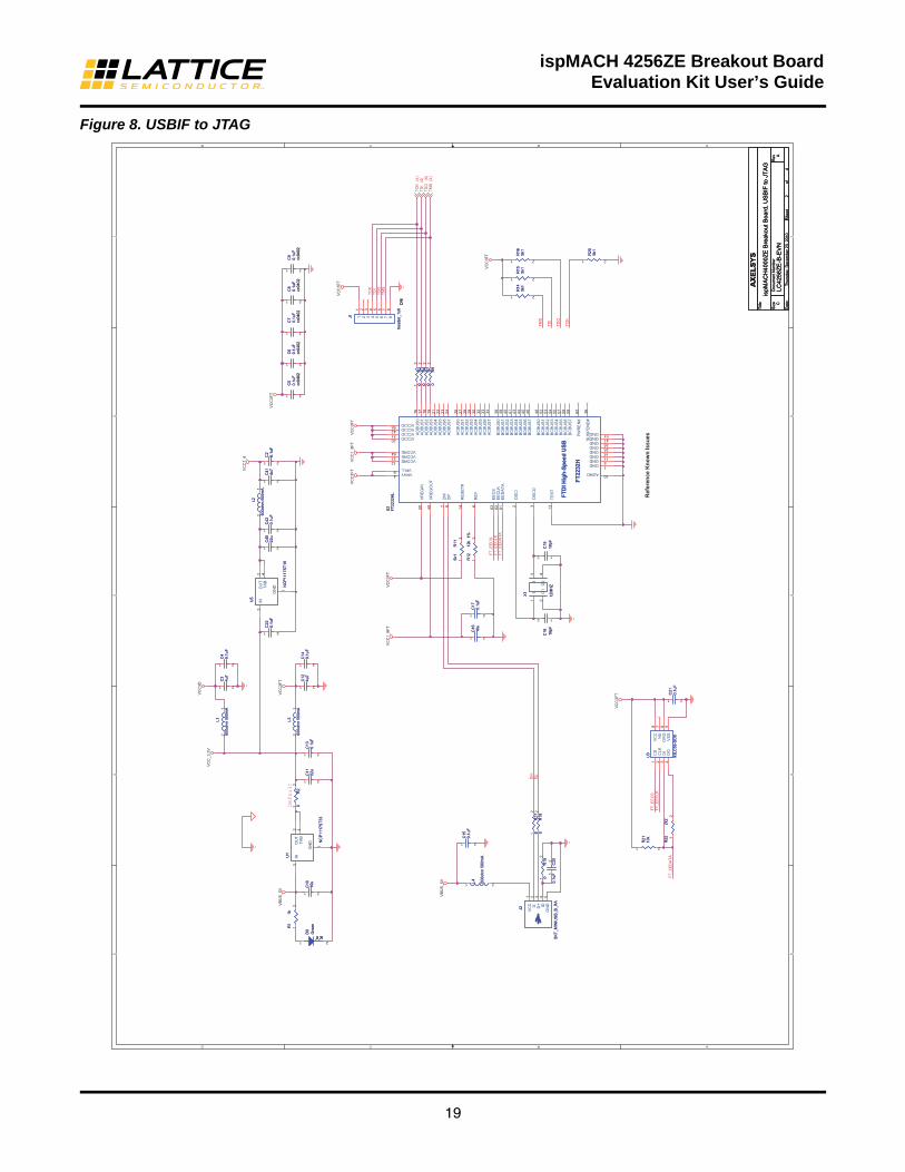
JTAG Interface Circuits (Reference Known Issues)For power and programming, a FTDI chip USB UART/FIFO IC converter provides a communication interface between a PC host and the JTAG programming chain of the Breakout Board. The USB 5V supply is also used as a source for the 3.3V and 1.8V supply rails. A USB mini-B socket is provided for the USB connector cable.
Table 8. JTAG Interface Reference
Item Description
Reference Designator U2
Part Number FT2232HL
Manufacturer Future Technology Devices International (FTDI)
Web Site www.ftdichip.com

14
ispMACH 4256ZE Breakout Board Evaluation Kit User’s Guide
Table 9. JTAG Programming Pin Information
Description ispMACH 4256ZE Pin
Test Data Output 107:TDO
Test Data Input 2:TDI
Test Mode Select 74:TMS
Test Clock 35:TCK
LEDsA green LED (D9) is used to indicate USB 5V power. Eight red LEDs are driven by I/O pins of the ispMACH 4256ZE CPLD.
Table 10. Power and User LEDs Reference
Item Description
Reference Designators D1, D2, D3, D4, D5, D6, D7, D8, D9
Part Number LTST-C190KRKT (D1-D8)LTST-C190KGKT (D9)
Manufacturer Lite-On It Corporation
Web Site www.liteonit.com
Power Supply3.3V and 1.8V supply rails are converted from the USB 5V interface when the board is connected to a host PC.
Test PointsIn order to check the various voltage levels used, test points are provided:
• TP1, VCC3D (VCCO Bank 0)
• TP2, VCC3D (VCCO Bank 1)
• TP3, VCC1_8 (VCC Core)
USB Programming and Debug Interface The USB mini-B socket of the Breakout Board serves as the programming and debug interface.
JTAG Programming: For JTAG programming, a preprogrammed USB PHY peripheral controller is provided on the Breakout Board to serve as the programming interface to the ispMACH 4256ZE CPLD.
Programming requires the ispVM System software.
Table 11. USB Interface Reference
Item Description
Reference Designator U2
Part Number FT2232HL
Manufacturer Future Technology Devices International (FTDI)
Web Site www.ftdichip.com
15
ispMACH 4256ZE Breakout Board Evaluation Kit User’s Guide
Board ModificationsThis section describes modifications to the board to change or add functionality.
Bypassing the USB Programming InterfaceThe USB programming interface circuit (section 6.2.8 USB Programming and Debug Interface) may be optionally bypassed by removing the 0 ohm resistors: R3, R4, R7, and R9 (See Schematic Sheet 2 of 4, Appendix A. Sche-matics). Header landing J1 provides JTAG signal access for jumper wires or a 1x8 pin header.
Applying External PowerThe Breakout Board is powered by the circuit of Schematic Sheet 2 of 4 based on the 5V USB power source. You may disconnect this power source by removing the 0 ohm resistors: R47 (VCCO 3.3V, Bank 0), R48 (VCCO 3.3V, Bank 1), and R53 (VCC 1.8V, Core). Power connections are available from the expansion header landing, J6, Schematic Sheet 3 of 4.
Measuring Bank and Core VoltagesTest points (TP1, TP2, and TP3) provide access to bank VCCO and VCC core power supplies of the ispMACH 4256ZE CPLD. 0 ohm resistors: R47 (VCCO 3.3V, Bank 0), R48 (VCCO 3.3V, Bank 1), and R53 (VCC 1.8V, Core) can be removed to add a current meter inline or add a resistor shunt to measure voltage across.
Mechanical SpecificationsDimensions: 3 in. [L] x 3 in. [W] x 1/2 in. [H]
Environmental RequirementsThe evaluation board must be stored between -40° C and 100° C. The recommended operating temperature is between 0° C and 90° C.
The board can be damaged without proper anti-static handling.
GlossaryCPLD: Complex Programmable Logic Device
LED: Light Emitting Diode
LUT: Look-Up Table
PCB: Printed Circuit Board
RoHS: Restriction of Hazardous Substances Directive
TQFP: Thin Quad Flat Pack
USB: Universal Serial Bus
WDT: Watchdog Timer

16
ispMACH 4256ZE Breakout Board Evaluation Kit User’s Guide
TroubleshootingUse the tips in this section to diagnose problems with the ispMACH 4256ZE Breakout Board.
LEDs Do Not Flash
If power is applied but the board does not flash according to the preprogrammed counter demonstration then it is likely that the board has been reprogrammed with a new design. Follow the directions in the Demonstration Designsection of this document to restore the factory default.
USB Cable Not Detected
If ispVM System does not recognize the USB cable even after installing the Lattice USB Port Drivers and rebooting, the incorrect USB driver may have been installed. This usually occurs if you attach the board to your PC prior to installing the USB driver or ispVM System software.
To access the Troubleshooting the USB Driver Installation Guide:
1. Start ispVM System and choose Options > Cable and I/O Port Setup.The Cable and I/O Port Setup Dialog appears.
2. Click the Troubleshooting the USB Driver Installation Guide link.The Troubleshooting the USB Driver Installation Guide document appears in your system’s PDF file reader.
3. Follow the directions of the guide to install the Lattice USB driver.
Determine the Source of a Pre-Programmed Device
You may receive your Breakout Board after it has been reprogrammed by someone else. To restore the board to the factory default, see the Download Demo Designs section for details on downloading and reprogramming the device.
You can also determine which demo design is currently programmed onto the Breakout Board by comparing the JEDEC checksums against of the programming file with what is read from the programmed part.
To compare JEDEC file checksum:
1. Connect the Breakout Board to a host PC using the USB port.
2. Start ispVM and choose ispTools > Scan.The device appears in the Device List.
3. Double-click the device row.The Device Information dialog appears.
4. Click the Browse button.The Save as Data File dialog appears.
5. Specify a new JEDEC Data File name and click the Save button.
6. From the Operation list choose Read and Save JEDEC and click OK.
7. Choose Project > Download.
ispVM reads the contents from the device and writes the results to the JEDEC file specified.
Open the JEDEC file into a text editor and page to the bottom of the file.
Note the hexidecimal checksum at the line above the User Electronic Data note line. Compare this value against the checksum of the original JEDEC demo programming files.
17
ispMACH 4256ZE Breakout Board Evaluation Kit User’s Guide
Ordering Information
Description Ordering Part NumberChina RoHS Environment-Friendly
Use Period (EFUP)
ispMACH 4256ZE Breakout Board Evaluation Kit LC4256ZE-B-EVN
Technical Support AssistanceHotline: 1-800-LATTICE (North America)
+1-503-268-8001 (Outside North America)e-mail: [email protected]: www.latticesemi.com
Revision HistoryDate Version Change Summary
March 2011 01.0 Initial release.
March 2012 01.1 Added Appendix C. Known Issues.
© 2012 Lattice Semiconductor Corp. All Lattice trademarks, registered trademarks, patents, and disclaimers are as listed at www.latticesemi.com/legal. All other brand or product names are trademarks or registered trademarks of their respective holders. The specifications and information herein are subject to change without notice.
18
ispMACH 4256ZE Breakout Board Evaluation Kit User’s Guide
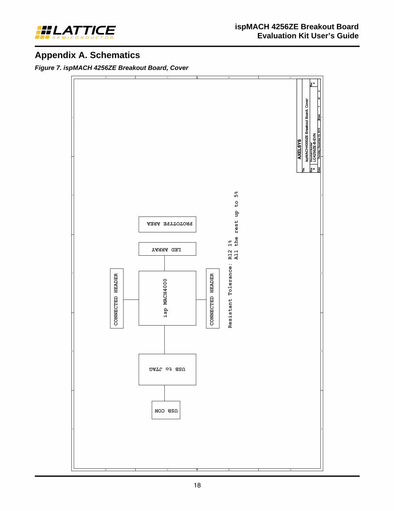
Appendix A. SchematicsFigure 7. ispMACH 4256ZE Breakout Board, Cover
5 5
4 4
3 3
2 2
1 1
DD
CC
BB
AA
Title
veR
rebmu
N tnemuco
DeziS
teehS:eta
Dof
AXE
LSYS
LC42
56ZE
-B-E
VN
A
ispM
AC
H40
00ZE
Bre
akou
t Boa
rd, C
over
B
14
Thur
sday
, Dec
embe
r 23,
201
0
Title
veR
rebmu
N tnemuco
DeziS
teehS:eta
Dof
AXE
LSYS
LC42
56ZE
-B-E
VN
A
ispM
AC
H40
00ZE
Bre
akou
t Boa
rd, C
over
B
14
Thur
sday
, Dec
embe
r 23,
201
0
Title
veR
rebmu
N tnemuco
DeziS
teehS:eta
Dof
AXE
LSYS
LC42
56ZE
-B-E
VN
A
ispM
AC
H40
00ZE
Bre
akou
t Boa
rd, C
over
B
14
Thur
sday
, Dec
embe
r 23,
201
0
USB CON
USB to JTAG
isp MACH4000
LED ARRAY
CONNECTED HEADER
CONNECTED HEADER
PROTOTYPE AREA
Resistant Tolerance: R12 1%
All the rest up to 5%
19
ispMACH 4256ZE Breakout Board Evaluation Kit User’s Guide
Figure 8. USBIF to JTAG5 5
4 4
3 3
2 2
1 1
DD
CC
BB
AA
Dm
Dp
FT_E
ECS
FT_E
ECLK
FT_E
EDAT
A
FT_E
EDAT
A
TMS
TDI
TDO
TCK
TCK
TDI
TDO
TMS
FT_E
ECS
FT_E
ECLK
VCC
3FT
VBU
S_5V
VCC
_3.3
V
VBU
S_5V
VCC
3D
VCC
3FT
VCC
3FT
VCC
3FT
VCC
1_8F
T
VCC
3FT
VCC
1_8F
T
VCC
3FT
VCC
3FT
VCC
3FT
VCC
1_8
TCK
(4)
TDI
(4)
TDO
(4)
TMS
(4)
Title
veR
rebmu
N tnemuco
DeziS
teehS:eta
Dof
AXE
LSYS
LC42
56ZE
-B-E
VN
A
ispM
AC
H40
00ZE
Bre
akou
t Boa
rd, U
SB
IF to
JTA
G
C
24
Thur
sday
, Dec
embe
r 23,
201
0
Title
veR
rebmu
N tnemuco
DeziS
teehS:eta
Dof
AXE
LSYS
LC42
56ZE
-B-E
VN
A
ispM
AC
H40
00ZE
Bre
akou
t Boa
rd, U
SB
IF to
JTA
G
C
24
Thur
sday
, Dec
embe
r 23,
201
0
Title
veR
rebmu
N tnemuco
DeziS
teehS:eta
Dof
AXE
LSYS
LC42
56ZE
-B-E
VN
A
ispM
AC
H40
00ZE
Bre
akou
t Boa
rd, U
SB
IF to
JTA
G
C
24
Thur
sday
, Dec
embe
r 23,
201
0
Default
21
R19
0R
190
VC
C1
D-
2D
+3
ID4
GN
D5
J2
SKT_
MIN
IUSB
_B_R
A
J2
SKT_
MIN
IUSB
_B_R
A
21
R14
5k1
R14
5k1
21
R17
0R
170
1 2
C40
22u
C40
22u
12
C19
18pF
C19
18pF
21
R11
5k1
R11
5k1
12
L3
600o
hm 5
00m
A
L3
600o
hm 5
00m
A
CS
1C
LK2
DI
3D
O4
VS
S5
OR
G6
NU
7V
CC
8
93LC
56-S
O8
U3
93LC
56-S
O8
U3
1 2
C8
0.1u
Fcc
0402
C8
0.1u
Fcc
0402
21
R21
10k
R21
10k
11
22
33
44
55
66
77
88
J1
head
er_1
x8D
NI
J1
head
er_1
x8D
NI
21
R2
0R
20
21
R7
0R
70
21
R15
5k1
R15
5k1
1 2
C13
0.1u
FC
130.
1uF
21R
11k
R1
1k
VR
EG
IN50
VR
EG
OU
T49
DM
7D
P8
RE
F6
RE
SE
T#14
EE
CS
63E
EC
LK62
EE
DA
TA61
OS
CI
2
OS
CO
3
TES
T13
AD
BU
S0
16A
DB
US
117
AD
BU
S2
18A
DB
US
319
VPHY4VPLL9
VCORE12VCORE37VCORE64
VCCIO20VCCIO31VCCIO42VCCIO56
AGND 10
GND 1GND 5GND 11GND 15GND 25GND 35GND 47GND 51P
WR
EN
#60
SU
SP
EN
D#
36
AD
BU
S4
21A
DB
US
522
AD
BU
S6
23A
DB
US
724
AC
BU
S0
26A
CB
US
127
AC
BU
S2
28A
CB
US
329
AC
BU
S4
30A
CB
US
532
AC
BU
S6
33A
CB
US
734
BD
BU
S0
38B
DB
US
139
BD
BU
S2
40B
DB
US
341
BD
BU
S4
43B
DB
US
544
BD
BU
S6
45B
DB
US
746
BC
BU
S0
48B
CB
US
152
BC
BU
S2
53B
CB
US
354
BC
BU
S4
55B
CB
US
557
BC
BU
S6
58B
CB
US
759
FTDI
Hig
h-Sp
eed
USB
F
T223
2H
FT22
32H
LU
2
FTDI
Hig
h-Sp
eed
USB
Refe
renc
e Kn
own
Issu
es
F
T223
2H
FT22
32H
LU
2
1 2
C4
0.1u
FC
40.
1uF
1 2
C9
0.1u
Fcc
0402
C9
0.1u
Fcc
0402
1 2
C22
0.1u
FC
220.
1uF
1 2
C7
0.1u
Fcc
0402
C7
0.1u
Fcc
0402
11
33
G1
2G
24
X1 12M
HZ
X1 12M
HZ
1 2
C17
0.1u
FC
170.
1uF
1 2
C2
0.1u
FC
20.
1uF
21R
1212
k1%
R12
12k
1%
1 2L4 600o
hm 5
00m
A
L4 600o
hm 5
00m
A
GN
D
1
IN3
OU
T2
TAB
4
U5
NC
P111
7ST1
8
U5
NC
P111
7ST1
8
21
R18
0R
180
1 2
C42
0.1u
FC
420.
1uF
12
C18 18pF
C18 18pF
12
C20
0.1u
FC
200.
1uF
21
R22
2k2
R22
2k2
21
R16
5k1
R16
5k1
1 2
D9
Gre
enD
9G
reen
1 2
C3
4u7
C3
4u7
1 2
C16
10u
C16
10u
1 2
C12
4u7
C12
4u7
12
L2
600o
hm 5
00m
A
L2
600o
hm 5
00m
A
21
R4
0R
40
1 2
C6
0.1u
Fcc
0402
C6
0.1u
Fcc
0402
1 2
C14
0.1u
FC
140.
1uF
1 2
C15
0.1u
FC
150.
1uF
1 2
C21
0.1u
FC
210.
1uF
1 2
C10
10u
C10
10u
1 2
C11
22u
C11
22u
12
L1
600o
hm 5
00m
A
L1
600o
hm 5
00m
A
21
R3
0R
30
21
R9
0R
90
1 2
C41
4u7
C41
4u7
21
R20
5k1
R20
5k1
GN
D
1
IN3
OU
T2
TAB
4
U1
NC
P111
7ST3
3
U1
NC
P111
7ST3
3
1 2
C5
0.1u
Fcc
0402
C5
0.1u
Fcc
0402
20
ispMACH 4256ZE Breakout Board Evaluation Kit User’s Guide
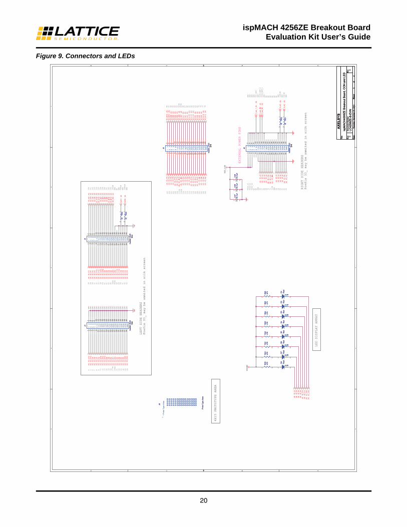
Figure 9. Connectors and LEDs5 5
4 4
3 3
2 2
1 1
DD
CC
BB
AA
VCC
_3.3
V
VCC
3D
CLK
0(4
)
CLK
1(4
)
CLK
2(4
)
CLK
3(4
)
IO_C
10(4
)
IO_C
6(4
)IO
_C8
(4)
IO_C
2(4
)IO
_C4
(4)
IO_D
12(4
)IO
_D14
(4)
IO_D
10(4
)
IO_D
6(4
)IO
_D8
(4)
IO_I
A1(4
)IO
_D4
(4)
IO_I
A2(4
)
IO_E
4(4
)IO
_E2
(4)
IO_E
8(4
)IO
_E6
(4)
IO_E
12(4
)IO
_E10
(4)
IO_F
4(4
)IO
_F2
(4)
IO_F
8(4
)IO
_F6
(4)
IO_F
12(4
)IO
_F10
(4)
IO_G
12(4
)
IO_I
A3(4
)
IO_G
8(4
)IO
_G10
(4)
IO_G
4(4
)IO
_G6
(4)
IO_I
A4(4
)
IO_G
2(4
)
IO_H
10(4
)IO
_H12
(4)
IO_H
6(4
)IO
_H8
(4)
IO_H
4(4
)IO
_H2
(4)
IO_A
4(4
)IO
_A2
(4)
IO_A
8(4
)IO
_A6
(4)
IO_A
10(4
)IO
_A12
(4)
IO_B
4(4
)IO
_B2
(4)
IO_B
8(4
)IO
_B6
(4)
IO_B
10(4
)IO
_B12
(4)
IO_I
A5(4
)
IO_C
12(4
)
IO_I
2(4
)IO
_I4
(4)
IO_I
6(4
)IO
_I8
(4) IO
_I10
(4)
IO_I
12(4
)
IO_J
2(4
)IO
_J4
(4)
IO_J
6(4
)IO
_J8
(4) IO
_J10
(4)
IO_J
12(4
)IO
_IB6
(4)
IO_K
12(4
)IO
_K10
(4)
IO_K
8(4
)IO
_K6
(4)
IO_K
4(4
)IO
_K2
(4)
IO_L
14(4
)IO
_L12
(4)
IO_L
10(4
)IO
_L8
(4)
IO_L
6(4
)IO
_L4
(4)
IO_I
B7(4
)IO
_IB8
(4)
IO_M
2(4
)IO
_M4
(4)
IO_M
6(4
)IO
_M8
(4)
IO_M
10(4
)IO
_M12
(4)
IO_N
2(4
)IO
_N4
(4)
IO_N
6(4
)IO
_N8
(4)IO
_N10
(4)
IO_N
12(4
)
IO_I
B9(4
)
IO_O
12(4
)IO
_O10
(4)
IO_O
8(4
)IO
_O6
(4)
IO_O
4(4
)IO
_O2
(4)IO
_IB1
0(4
)IO
_P12
(4)
IO_P
10(4
)IO
_P8
(4)
IO_P
6(4
)IO
_P4
(4)
IO_P
2(4
)
IO_I
2(4
)IO
_I4
(4)
IO_I
6(4
)IO
_I8
(4) IO
_I10
(4)
IO_I
12(4
)
IO_J
12(4
)IO
_J10
(4)
V_ex
t_B0
(4)
V_ex
t_B1
(4)
V_ex
t_1_
8v(4
)
Title
veR
rebmu
N tnemuco
DeziS
teehS:eta
Dof
AXE
LSYS
LC42
56ZE
-B-E
VN
A
ispM
AC
H40
00ZE
Bre
akou
t Boa
rd, C
ON
and
LE
D
C
34
Thur
sday
, Dec
embe
r 23,
201
0
Title
veR
rebmu
N tnemuco
DeziS
teehS:eta
Dof
AXE
LSYS
LC42
56ZE
-B-E
VN
A
ispM
AC
H40
00ZE
Bre
akou
t Boa
rd, C
ON
and
LE
D
C
34
Thur
sday
, Dec
embe
r 23,
201
0
Title
veR
rebmu
N tnemuco
DeziS
teehS:eta
Dof
AXE
LSYS
LC42
56ZE
-B-E
VN
A
ispM
AC
H40
00ZE
Bre
akou
t Boa
rd, C
ON
and
LE
D
C
34
Thur
sday
, Dec
embe
r 23,
201
0
4X15 PROTOTYPE AREA
LED DISPLAY ARRAY
EXTERNAL POWER PINS
LEFT SIDE HEADERS
Prefix IO_ may be ommited in silk screen
RIGHT SIDE HEADERS
Prefix IO_ may be ommited in silk screen
4 5 6 7 8 9 11 12 13 14 15 16 17IN
20IN
21 22 23 24 25 26
GND
GND
GND
GND
GND
GND
GND
GND
GND
GND
GND
GND
GND
GND
GND
GND
GND
GND
GND
GND
28 29 30 31 32 33 39 40 41 42 43 44 38IN
45IN
48 49 50 51 52 53
130
131
132
133
134
135
138
139
140
141
142
143
144I
NGN
DNC GN
D54
CLK
GND
128C
LKGN
D
125
124
123
122
121
120
117I
N11
0IN
116
115
114
113
112
111
105
104
103
102
101
100
98 97 96 95 94 93 92IN
89IN
88 87 86 85 84 83 81 80 79 78 77 76
VCCO
_33
VCCO
_33
VCCO
_33
NC NC GND
66 67 68 69 70 71 72IN
GND
58 59 60 61 62 63
GND
GND
GND
GND
VCC_
EXT
GND
VCCO
_EXT
_0VC
CO_E
XT_1
GND
NC NC NC NC NC NC GND
126C
LKGN
D56
CLK
GND
21
R50
10R
5010
21
R41
470
R41
470
1 2
D2
Red
D2
Red
21
R44
470
R44
470
Pro
to T
ype
Are
a1
J9
Prot
o Ty
pe A
rea
J9
Prot
o Ty
pe A
rea
1 2
C28
0.1u
FC
280.
1uF
11
22
33
44
55
66
77
88
99
1010
1111
1212
1313
1414
1515
1616
1717
1818
1919
2020
2121
2222
2323
2424
2525
2626
2727
2828
2929
3030
3131
3232
3333
3434
3535
3636
3737
3838
3939
4040
J3
head
er_2
x20
DN
I
J3
head
er_2
x20
DN
I
1 2
D1
Red
D1
Red
21
R46
470
R46
470
21
R45
470
R45
470
21
R49
10R
4910
21
R43
470
R43
470
21
R40
470
R40
470
1 2
C27
0.1u
FC
270.
1uF
21
R39
470
R39
470
1 2
D8
Red
D8
Red
11
22
33
44
55
66
77
88
99
1010
1111
1212
1313
1414
1515
1616
1717
1818
1919
2020
2121
2222
2323
2424
2525
2626
2727
2828
2929
3030
3131
3232
3333
3434
3535
3636
3737
3838
3939
4040
J6
head
er_2
x20
DN
I
J6
head
er_2
x20
DN
I
1 2
D6
Red
D6
Red
21
R52
10R
5210
1 2
C29
0.1u
FC
290.
1uF
1 2
D5
Red
D5
Red
1 2
D4
Red
D4
Red
1 2
D7
Red
D7
Red
21
R51
10R
5110
11
22
33
44
55
66
77
88
99
1010
1111
1212
1313
1414
1515
1616
1717
1818
1919
2020
2121
2222
2323
2424
2525
2626
2727
2828
2929
3030
3131
3232
3333
3434
3535
3636
3737
3838
3939
4040
J5
head
er_2
x20
DN
I
J5
head
er_2
x20
DN
I
21
R42
470
R42
470
1 2
D3
Red
D3
Red
11
22
33
44
55
66
77
88
99
1010
1111
1212
1313
1414
1515
1616
1717
1818
1919
2020
2121
2222
2323
2424
2525
2626
2727
2828
2929
3030
3131
3232
3333
3434
3535
3636
3737
3838
3939
4040
J4
head
er_2
x20
DN
I
J4
head
er_2
x20
DN
I
21
ispMACH 4256ZE Breakout Board Evaluation Kit User’s Guide
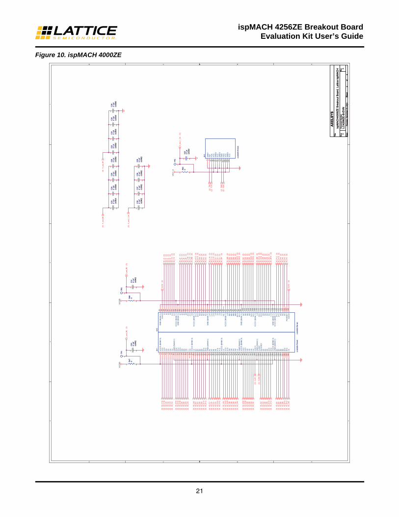
Figure 10. ispMACH 4000ZE5 5
4 4
3 3
2 2
1 1
DD
CC
BB
AA
VCC
3D
VCC
1_8
VCC
3D
TCK
(2)
TDI
(2) TD
O(2
)TM
S(2
)
CLK
0(3
)
CLK
1(3
)
CLK
2(3
)
CLK
3(3
)
V_ex
t_B1
(3)
V_ex
t_B0
(3)
IO_C
12(3
)IO
_C10
(3)
IO_C
6(3
)IO
_C8
(3)
IO_C
2(3
)IO
_C4
(3)
IO_D
12(3
)IO
_D14
(3)
IO_D
10(3
)
IO_D
6(3
)IO
_D8
(3)
IO_I
A1(3
)IO
_D4
(3)
IO_I
A2(3
)
IO_E
4(3
)IO
_E2
(3)
IO_E
8(3
)IO
_E6
(3)
IO_E
12(3
)IO
_E10
(3)
IO_F
4(3
)IO
_F2
(3)
IO_F
8(3
)IO
_F6
(3)
IO_F
12(3
)IO
_F10
(3)
IO_G
12(3
)IO
_IA3
(3)
IO_G
8(3
)IO
_G10
(3)
IO_G
4(3
)IO
_G6
(3)
IO_I
A4(3
)IO
_G2
(3)
IO_H
10(3
)IO
_H12
(3)
IO_H
6(3
)IO
_H8
(3)
IO_H
4(3
)IO
_H2
(3)
IO_A
4(3
)IO
_A2
(3)
IO_A
8(3
)IO
_A6
(3)
IO_A
10(3
)IO
_A12
(3)
IO_B
4(3
)IO
_B2
(3)
IO_B
8(3
)IO
_B6
(3)
IO_B
10(3
)IO
_B12
(3)
IO_I
A5(3
)
IO_I
2(3
)IO
_I4
(3)
IO_I
6(3
)IO
_I8
(3)
IO_I
10(3
)IO
_I12
(3)
IO_J
2(3
)IO
_J4
(3)
IO_J
6(3
)IO
_J8
(3)
IO_J
10(3
)IO
_J12
(3)
IO_I
B6(3
)
IO_K
12(3
)IO
_K10
(3)
IO_K
8(3
)IO
_K6
(3)
IO_K
4(3
)IO
_K2
(3)
IO_L
14(3
)IO
_L12
(3)
IO_L
10(3
)IO
_L8
(3)
IO_L
6(3
)IO
_L4
(3)
IO_I
B7(3
)
IO_I
B8(3
)IO
_M2
(3)
IO_M
4(3
)IO
_M6
(3)
IO_M
8(3
)IO
_M10
(3)
IO_M
12(3
)
IO_N
2(3
)IO
_N4
(3)
IO_N
6(3
)IO
_N8
(3)
IO_N
10(3
)IO
_N12
(3)
IO_I
B9(3
)IO
_O12
(3)
IO_O
10(3
)IO
_O8
(3)
IO_O
6(3
)IO
_O4
(3)
IO_O
2(3
)IO
_IB1
0(3
)
IO_P
12(3
)IO
_P10
(3)
IO_P
8(3
)IO
_P6
(3)
IO_P
4(3
)IO
_P2
(3)
V_ex
t_B0
(3)
V_ex
t_B1
(3)
V_ex
t_1_
8v(3
)
V_ex
t_1_
8v(3
)
Title
veR
rebmu
N tnemuco
DeziS
teehS:eta
Dof
AXE
LSYS
LC42
56ZE
-B-E
VN
A
ispM
AC
H40
00ZE
Bre
akou
t Boa
rd, L
attic
e is
pMA
CH
C
44
Thur
sday
, Dec
embe
r 23,
201
0
Title
veR
rebmu
N tnemuco
DeziS
teehS:eta
Dof
AXE
LSYS
LC42
56ZE
-B-E
VN
A
ispM
AC
H40
00ZE
Bre
akou
t Boa
rd, L
attic
e is
pMA
CH
C
44
Thur
sday
, Dec
embe
r 23,
201
0
Title
veR
rebmu
N tnemuco
DeziS
teehS:eta
Dof
AXE
LSYS
LC42
56ZE
-B-E
VN
A
ispM
AC
H40
00ZE
Bre
akou
t Boa
rd, L
attic
e is
pMA
CH
C
44
Thur
sday
, Dec
embe
r 23,
201
0
GN
D1
1TD
I2
TCK
35V
CC
36G
ND
237
VC
C57
GN
D3
73TM
S74
TDO
107
VC
C10
8G
ND
410
9V
CC
129
LC42
56ZE
-5TN
144C
U4-
3
LC42
56ZE
-5TN
144C
U4-
3
1 2
C32
0.1u
Fcc
0402
C32
0.1u
Fcc
0402
1 2
C24
0.1u
Fcc
0402
C24
0.1u
Fcc
0402
1 2
C37
0.1u
Fcc
0402
C37
0.1u
Fcc
0402
1 2
C39
0.1u
Fcc
0402
C39
0.1u
Fcc
0402
GN
D (B
AN
K 1
)55
CLK
2/I
56I2
58I4
59I6
60I8
61I1
062
I12
63V
CC
O (B
AN
K 1
)64
GN
D (B
AN
K 1
)65
J266
J467
J668
J869
J10
70J1
271
I-672
VC
CO
(BA
NK
1)
75K
1276
K10
77K
878
K6
79K
480
K2
81G
ND
(BA
NK
1)
82L1
483
L12
84L1
085
L886
L687
L488
I-789
NC
90V
CC
O (B
AN
K 1
)91
I-892
M2
93M
494
M6
95M
896
M10
97M
1298
GN
D (B
AN
K 1
)99
N2
100
N4
101
N6
102
N8
103
N10
104
N12
105
VC
CO
(BA
NK
1)
106
I-911
0O
1211
1O
1011
2O
811
3O
611
4O
411
5O
211
6I-1
011
7G
ND
(BA
NK
1)
118
VC
CO
(BA
NK
1)
119
P12
120
P10
121
P8
122
P6
123
P4
124
P2/
GO
E1
125
CLK
3/I
126
LC42
56ZE
-5TN
144C
U4-
2
LC42
56ZE
-5TN
144C
U4-
2
1 2
C43
0.1u
Fcc
0402
C43
0.1u
Fcc
0402
21
R53
0R53
0
21
R47
0R47
0
1 2
C30
0.1u
Fcc
0402
C30
0.1u
Fcc
0402
1 2
C36
0.1u
Fcc
0402
C36
0.1u
Fcc
0402
1
TP1
TP1
1 2
C31
0.1u
Fcc
0402
C31
0.1u
Fcc
0402
1
TP3
TP3
1 2
C26
0.1u
Fcc
0402
C26
0.1u
Fcc
0402
1 2
C33
0.1u
Fcc
0402
C33
0.1u
Fcc
0402
VC
CO
(BA
NK
0)
3C
124
C10
5C
86
C6
7C
48
C2
9G
ND
(BA
NK
0)
10D
1411
D12
12D
1013
D8
14D
615
D4
16I-1
17N
C18
VC
CO
(BA
NK
0)
19I-2
20E
221
E4
22E
623
E8
24E
1025
E12
26G
ND
(BA
NK
0)
27F2
28F4
29F6
30F8
31F1
032
F12
33V
CC
O (B
AN
K 0
)34
I-338
G12
39G
1040
G8
41G
642
G4
43G
244
I-445
GN
D (B
AN
K 0
)46
VC
CO
(BA
NK
0)
47H
1248
H10
49H
850
H6
51H
452
H2
53C
LK1/
I54
GN
D (B
AN
K 0
)12
7C
LK0/
I12
8A
2/G
OE
013
0A
413
1A
613
2A
813
3A
1013
4A
1213
5V
CC
O (B
AN
K 0
)13
6G
ND
(BA
NK
0)
137
B2
138
B4
139
B6
140
B8
141
B10
142
B12
143
I-514
4
LC42
56ZE
-5TN
144C
U4-
1
LC42
56ZE
-5TN
144C
U4-
1
1 2
C23
0.1u
Fcc
0402
C23
0.1u
Fcc
0402
21
R48
0R48
0
1 2
C34
0.1u
Fcc
0402
C34
0.1u
Fcc
0402
1 2
C35
0.1u
Fcc
0402
C35
0.1u
Fcc
0402
1 2
C25
0.1u
Fcc
0402
C25
0.1u
Fcc
0402
1 2
C38
0.1u
Fcc
0402
C38
0.1u
Fcc
0402
1
TP2
TP2
22
ispMACH 4256ZE Breakout Board Evaluation Kit User’s Guide
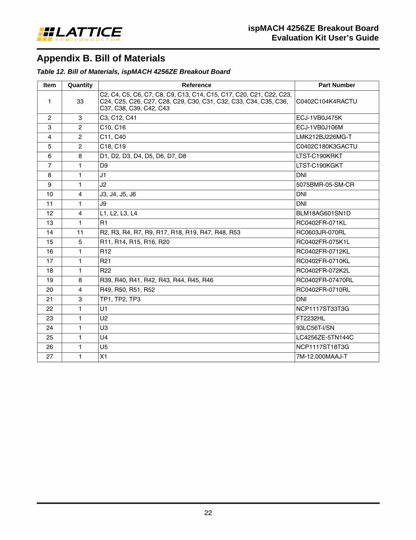
Appendix B. Bill of MaterialsTable 12. Bill of Materials, ispMACH 4256ZE Breakout Board
Item Quantity Reference Part Number
1 33C2, C4, C5, C6, C7, C8, C9, C13, C14, C15, C17, C20, C21, C22, C23, C24, C25, C26, C27, C28, C29, C30, C31, C32, C33, C34, C35, C36, C37, C38, C39, C42, C43
C0402C104K4RACTU
2 3 C3, C12, C41 ECJ-1VB0J475K
3 2 C10, C16 ECJ-1VB0J106M
4 2 C11, C40 LMK212BJ226MG-T
5 2 C18, C19 C0402C180K3GACTU
6 8 D1, D2, D3, D4, D5, D6, D7, D8 LTST-C190KRKT
7 1 D9 LTST-C190KGKT
8 1 J1 DNI
9 1 J2 5075BMR-05-SM-CR
10 4 J3, J4, J5, J6 DNI
11 1 J9 DNI
12 4 L1, L2, L3, L4 BLM18AG601SN1D
13 1 R1 RC0402FR-071KL
14 11 R2, R3, R4, R7, R9, R17, R18, R19, R47, R48, R53 RC0603JR-070RL
15 5 R11, R14, R15, R16, R20 RC0402FR-075K1L
16 1 R12 RC0402FR-0712KL
17 1 R21 RC0402FR-0710KL
18 1 R22 RC0402FR-072K2L
19 8 R39, R40, R41, R42, R43, R44, R45, R46 RC0402FR-07470RL
20 4 R49, R50, R51, R52 RC0402FR-0710RL
21 3 TP1, TP2, TP3 DNI
22 1 U1 NCP1117ST33T3G
23 1 U2 FT2232HL
24 1 U3 93LC56T-I/SN
25 1 U4 LC4256ZE-5TN144C
26 1 U5 NCP1117ST18T3G
27 1 X1 7M-12.000MAAJ-T

23
ispMACH 4256ZE Breakout Board Evaluation Kit User’s Guide
Appendix C. Known Issues1. The ispMACH 4000ZE 1532 interface signals TCK, TMS, TDI and TDO are referenced to VCC=1.8V (logic
core). The ispMACH 4256ZE Breakout Board has an issue where the JTAG signals are connected to the FTDI which has a 3.3V interface. This circuit should not be replicated in a production board. As a work-around another FTDI device could be selected or a level translator could be used between the FTDI device and the ispMACH 4000ZE.