ds5000fp soft microprocessor chip - analog, linear, and mixed
TRANSCRIPT


DS5000FP
2 of 22
DESCRIPTION The DS5000FP Soft Microprocessor Chip is an 8051-compatible processor based on NV RAM technology. It is substantially more flexible than a standard 8051, yet provides full compatibility with the 8051 instruction set, timers, serial port, and parallel I/O ports. By using NV RAM instead of ROM, the user can program and then reprogram the microcontroller while in-system. The application software can even change its own operation, which allows frequent software upgrades, adaptive programs, customized systems, etc. In addition, by using NV SRAM, the DS5000FP is ideal for data-logging applications and it connects easily to a Dallas real-time clock for time stamp and date. The DS5000FP provides the benefits of NV RAM without using I/O resources. It uses a nonmultiplexed byte-wide address and data bus for memory access. This bus can perform all memory access and provides decoded chip enables for SRAM. This leaves the 32 I/O port pins free for application use. The DS5000FP uses ordinary SRAM and battery backs the memory contents with a user’s external lithium cell. Data is maintained for over 10 years with a very small lithium cell. A DS5000FP also provides crash-proof operation in portable systems or systems with unreliable power. These features include the ability to save the operating state, Power-fail Reset, Power-fail Interrupt, and Watchdog Timer. A user loads programs into the DS5000FP via its on-chip Serial Bootstrap Loader. This function supervises the loading of code into NV RAM, validates it, and then becomes transparent to the user. Software can be stored in an 8-kbyte or 32-kbyte CMOS SRAM. Using its internal Partitioning, the DS5000FP will divide this common RAM into user programmable code and data segments. This Partition can be selected at program loading time, but can be modified anytime later. It will decode memory access to the SRAM, communicate via its byte-wide bus and write-protect the memory portion designated as ROM. Combining program and data storage in one device saves board space and cost. The DS5000FP can also access a second 32 kbytes of NV RAM but this area is restricted to data memory. The DS2250(T) and DS5000(T) are available for a user who wants a pre-constructed module using the DS5000FP, RAM, lithium cell, and optional real-time clock. Each device is described in separate data sheets, available on our website at www.maxim-ic.com/microcontrollers. More details are contained in the Secure Microcontroller User’s Guide.

DS5000FP
3 of 22
DS5000FP BLOCK DIAGRAM Figure 1

DS5000FP
4 of 22
PIN DESCRIPTION PIN NAME FUNCTION
15, 17, 19, 21, 25, 27, 29, 31 P1.0–P1.7 General-Purpose I/O Port 1
34 RST Active-High Reset Input. A logic 1 applied to this pin activates a reset state. This pin is pulled down internally so this pin can be left unconnected if not used.
36 P3.0/ RXD
General-Purpose I/O Port Pin 3.0. Also serves as the receive signal for the on board UART. This pin should not be connected directly to a PC COM port.
38 P3.1/ TXD
General-Purpose I/O Port Pin 3.1. Also serves as the transmit signal for the on-board UART. This pin should not be connected directly to a PC COM port.
39 P3.2/INT0
General-Purpose I/O Port Pin 3.2. Also serves as the active-low External Interrupt 0.
40 P3.3/INT1
General-Purpose I/O Port Pin 3.3. Also serves as the active-low External Interrupt 1.
41 P3.4/T0 General-Purpose I/O Port Pin 3.4. Also serves as the Timer 0 input. 44 P3.5/T1 General-Purpose I/O Port Pin 3.5. Also serves as the Timer 1 input.
45 P3.6/ WR General-Purpose I/O Port Pin. Also serves as the write strobe for expanded bus operation.
46 P3.7/ RD General-Purpose I/O Port Pin. Also serves as the read strobe for expanded bus operation.
47, 48 XTAL2, XTAL1
Crystal Connections. Used to connect an external crystal to the internal oscillator. XTAL1 is the input to an inverting amplifier and XTAL2 is the output.
52, 53 GND Logic Ground 49, 50, 51, 56, 58, 60, 64, 66 P2.0–P2.7 General-Purpose I/O Port 2. Also serves as the MSB of the expanded address
bus.
68 PSEN
Program Store Enable. This active-low signal is used to enable an external program memory when using the expanded bus. It is normally an output and should be unconnected if not used. PSEN is also used to invoke the Bootstrap Loader. At this time, PSEN will be pulled down externally. This should only be done once the DS5000FP is already in a reset state. The device that pulls down should be open drain since it must not interfere with PSEN under normal operation.
70 ALE
Address Latch Enable. Used to de-multiplex the multiplexed Expanded Address/Data bus on Port 0. This pin is normally connected to the clock input on a ’373 type transparent latch. When using a parallel programmer, this pin also assumes the PROG function for programming pulses.
73 EA
External Access. This pin forces the DS5000FP to behave like an 8031. No internal memory (or clock) will be available when this pin is at a logic low. Since this pin is pulled down internally, it should be connected to +5V to use NV RAM. In a parallel programmer, this pin also serves as VPP for super voltage pulses.

DS5000FP
5 of 22
PIN DESCRIPTION (continued) PIN NAME FUNCTION
11, 9, 7, 5, 1, 79, 77, 75 P0.0–P0.7
General-Purpose I/O Port 0. This port is open-drain and cannot drive a logic 1. It requires external pullups. Port 0 is also the multiplexed Expanded Address/Data bus. When used in this mode, it does not require pullups.
13, 14 VCC Power Supply, +5V
16, 8, 18, 80, 76, 4, 6, 20, 24, 26, 28, 30, 33,
35, 37
BA14–BA0
Byte-Wide Address Bus Bits 14–0. This 15-bit bus is combined with the nonmultiplexed data bus (BD7–BD0) to access NV SRAM. Decoding is performed on CE1 and CE2 . Read/write access is controlled by R/W. BA14–BA0 connect directly to an 8k or 32k SRAM. If an 8k RAM is used, BA13 and BA14 are unconnected. Note: BA13 and BA14 are inverted from the true logical address. BA14 is lithium backed.
71, 69, 67, 65, 61, 59, 57, 55 BD7–BD0
Byte-Wide Data Bus Bits 7–0. This 8-bit bidirectional bus is combined with the nonmultiplexed address bus (BA14–BA0) to access NV SRAM. Decoding is performed on CE1 and CE2 . Read/write access is controlled by R/W. BD7–BD0 connect directly to an 8k or 32k SRAM, and optionally to a real-time clock.
10 R/W Read/Write (Active Low). This signal provides the write enable to the SRAMs on the byte-wide bus. It is controlled by the memory map and partition. The blocks selected as Program (ROM) is write protected.
74 CE1
Active-Low Chip Enable 1. This is the primary decoded chip enable for memory access on the byte-wide bus. It connects to the chip enable input of one SRAM. CE1 is lithium backed. It will remain in a logic high inactive state when VCC falls below VLI.
78 CE2
Active-Low Chip Enable 2. This chip enable is provided to bank switch to a second block of 32k bytes of nonvolatile data memory. It connects to the chip enable input of one SRAM or one lithium-backed peripheral such a real-time clock. CE2 is lithium backed. It will remain in a logic high inactive state when VCC falls below VLI.
12 VCCO
VCC Output. This is switched between VCC and VLI by internal circuits based on the level of VCC. When power is above the lithium input, power will be drawn from VCC. The lithium cell remains isolated from a load. When VCC is below VLI, the VCCO switches to the VLI source. VCCO is connected to the VCC pin of an SRAM.
54 VLI Lithium Voltage Input. Connect to a lithium cell greater than VLImin and no greater than VLImax as shown in the electrical specifications. Nominal value is +3V.
2, 3, 22, 23, 32, 42, 43, 62, 63,
72 N.C. No Connection. Do not connect.

DS5000FP
6 of 22
INSTRUCTION SET The DS5000FP executes an instruction set that is object code compatible with the industry standard 8051 microcontroller. As a result, software development packages such as assemblers and compilers that have been written for the 8051 are compatible with the DS5000FP. A complete description of the instruction set and operation are provided in the Secure Microcontroller User’s Guide. Also note that the DS5000FP is embodied in the DS5000(T) and DS2250(T) modules. The DS5000(T) combines the DS5000FP with one SRAM of either 8 or 32 kbytes and a lithium cell. An optional Real Time Clock is also available in the DS5000T. This is packaged in a 40-pin DIP module. The DS2250(T) is an identical function in a SIMM form factor. It also offers the option of a second 32k SRAM mapped as data on Chip Enable 2. MEMORY ORGANIZATION Figure 2 illustrates the memory map accessed by the DS5000FP. The entire 64k of program and 64k of data is available. The DS5000FP maps 32k of this space into the SRAM connected to the byte-wide bus. This is the area from 0000h to 7FFFh (32k) and is reached via CE1 . Any area not mapped into the NV RAM is reached via the Expanded bus on Ports 0 & 2. Selecting CE2 provides another 32k of potential data storage. When CE2 is used, no data is available on the ports. The memory map is covered in detail in the Secure Microcontroller User’s Guide. Figure 3 illustrates a typical memory connection for a system using 8k bytes of SRAM. Figure 4 shows a similar system with 32 kbytes. The byte-wide Address bus connects to the SRAM address lines. The bi-directional byte-wide data bus connects the data I/O lines of the SRAM. CE1 provides the chip enable and R/ W is the write enable. An additional RAM could be connected to CE2 , with common connections for R/ W , BA14-0, and BD7-0.

DS5000FP
7 of 22
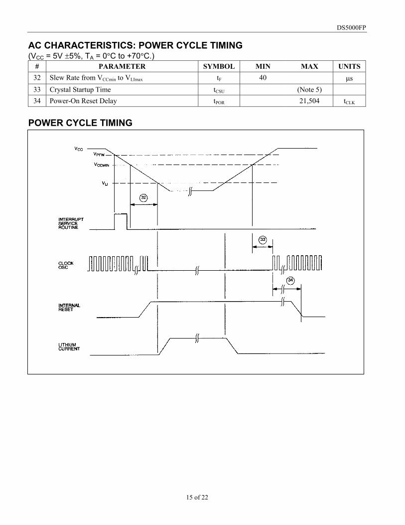
POWER MANAGEMENT The DS5000FP monitors power to provide Power-Fail Reset, early warning Power-Fail Interrupt, and switchover to lithium backup. It uses the lithium cell at VLI as a reference in determining the switch points. These are called VPFW, VCCMIN, and VLI respectively. When VCC drops below VPFW, the DS5000FP will perform an interrupt vector to location 2Bh if the power-fail warning was enabled. Full processor operation continues regardless. When power falls further to VCCMIN, the DS5000FP invokes a reset state. No further code execution will be performed unless power rises back above VCCMIN. CE1 , CE2 , R/ W go to an inactive (logic 1) state. Any address lines that are high (due to encryption) will follow VCC, except for BA14, which is lithium backed. VCC is still the power source at this time. When VCC drops further to below VLI, internal circuitry will switch to the lithium cell for power. The majority of internal circuits will be disabled and the remaining nonvolatile states will be retained. The lithium cell will power any devices connected to VCCO at this time. VCCO will be at the lithium battery voltage less a diode drop. This drop will vary depending on the load. Low-leakage SRAMs should be used for this reason. When a module is used, the lithium cell is selected by Dallas so absolute specifications are provided for the switch thresholds. When using the DS5000FP, the user must select the appropriate battery. The following formulas apply to the switch function:
VPFW = 1.45 x VLI VCCMIN = 1.40 x VLI
VLI Switch = 1.0 x VLI
MEMORY MAP OF THE DS5000FP Figure 2

DS5000FP
8 of 22
DS5000FP CONNECTION TO 8k X 8 SRAM Figure 3
DS5000FP CONNECTION TO 32k X 8 SRAM Figure 4

DS5000FP
9 of 22
ABSOLUTE MAXIMUM RATINGS Voltage Range on Any Pin Relative to Ground……………………………………...………-0.3V to + (VCC + 0.5V) Voltage Range on VCC Relative to Ground…………………….……….……………………..………-0.3V to +7.0V Operating Temperature Range………………………………….….………………………………..…..0°C to +70°C Storage Temperature Range……………………………………...………………………………..…..-40°C to +70°C Soldering Temperature Range……………………………………………..See IPC/JEDEC J-STD-020 Specification
This is a stress rating only and functional operation of the device at these or any other conditions beyond those indicated in the operation sections of this specification is not implied. Exposure to absolute maximum rating conditions for extended periods of time can affect reliability.
DC CHARACTERISTICS (VCC = 5V �5%, TA = 0�C to +70�C.)
PARAMETER SYMBOL MIN TYP MAX UNITS NOTES Input Low Voltage VIL -0.3 0.8 V 1 Input High Voltage VIH1 2.0 VCC +0.3 V 1 Input High Voltage RST, XTAL1 VIH2 3.5 VCC + 0.3 V 1 Output Low Voltage at IOL = 1.6mA (Ports 1, 2, 3) VOL1 0.15 0.45 V
Output Low Voltage at IOL = 3.2mA (Ports 0, ALE, PSEN , BA14–BA0, BD7–BD0, R/W, CE1-2)
VOL2 0.15 0.45 V 1
Output High Voltage at IOH = -80�A (Ports 1, 2, 3) VOH1 2.4 4.8 V 1
Output High Voltage at IOH = -400�A (Ports 0, ALE, PSEN, BA14–BA0, BD7–BD0, R/W, CE1-2)
VOH2 2.4 4.8 V 1
Input Low Current VIN = 0.45V (Ports 1, 2, 3) IIL -50 �A
Transition Current; 1 to 0 VIN = 2.0V (Ports 1, 2, 3) ITL -500 �A
Input Leakage Current 0.45 < VIN < VCC (Port 0) IL �10 �A
RST, EA Pulldown Resistor RRE 40 125 k�
Stop Mode Current ISM 80 �A 4 Power-Fail Warning Voltage VPFW 4.15 4.6 4.75 V 1, 6 Minimum Operating Voltage VCCmin 4.05 4.5 4.65 V 1, 6 Operating Voltage VCC VCC(MIN) 5.5 V 1, 6 Lithium Supply Voltage VLI 2.9 3.3 V 1 Programming Supply Voltage (Parallel Program Mode) VPP 12.5 13 V 1
Program Supply Current IPP 15 20 mA

DS5000FP
10 of 22
DC CHARACTERISTICS (continued) (VCC = 5V �5%, TA = 0°C to +70°C.)
PARAMETER SYMBOL MIN TYP MAX UNITS NOTES Operating Current at 16MHz ICC 36 mA 2 Idle Mode Current at 12MHz IIDLE 6.2 mA 3 Output Supply Voltage VCCO1 VCC - 0.3 V 1 Output Supply Voltage (Battery-Backed Mode) VCCO2 VLI - 0.65 VLI - 0.5 V 8
Output Supply Current at VCCO = VCC - 0.3V ICCO1 80 mA 2
Battery-Backed Quiescent Current ILI 5 75 nA 7 NOTES: 1. All voltages are referenced to ground. 2. Maximum operating ICC is measured with all output pins disconnected; XTAL1 driven with tCLKR,
tCLKF = 10ns, VIL = 0.5V; XTAL2 disconnected; EA = RST = PORT0 = VCC. 3. Idle mode ICC is measured with all output pins disconnected; XTAL1 driven at 12MHz with tCLKR,
tCLKF = 10ns, VIL = 0.5V; XTAL2 disconnected; EA = PORT0 = VCC, RST = VSS. 4. Stop mode ICC is measured with all output pins disconnected; EA = PORT0 = VCC; XTAL2 not
connected; RST = VSS. 5. Crystal startup time is the time required to get the mass of the crystal into vibrational motion from the
time that power is first applied to the circuit until the first clock pulse is produced by the on-chip oscillator. The user should check with the crystal vendor for the worst-case spec on this time.
6. Assumes VLI = 3.3V maximum. 7. ILI is the current drawn from VLI when VCC = 0V and VCCO is disconnected. 8. I CCO = 10�A.

DS5000FP
11 of 22
AC CHARACTERISTICS: EXPANDED BUS MODE TIMING SPECIFICATIONS (VCC = 5V �5%, TA = 0�C to +70�C.)
# PARAMETER SYMBOL MIN MAX UNITS 1 Oscillator Frequency 1/tCLK 1.0 16 MHz 2 ALE Pulse Width tALPW 2tCLK -40 ns 3 Address Valid to ALE Low tAVALL tCLK -40 ns 4 Address Hold After ALE Low tAVAAV tCLK -35 ns
at 12MHz 4tCLK -150 5 ALE Low to Valid Instruction In
at 16MHz tALLVI
4tCLK -90 ns
6 ALE Low to PSEN Low tALLPSL tCLK -25 ns
7 PSEN Pulse Width tPSPW 3tCLK -35 ns
at 12MHz 3tCLK -150 8 PSEN Low to Valid Instruction In
at 16MHz tPSLVI
3tCLK -90 ns
9 Input Instruction Hold after PSEN Going High tPSIV 0 ns
10 Input Instruction Float after PSEN Going High tPSIX tCLK -20 ns
11 Address Hold after PSEN Going High tPSAV tCLK -8 ns
at 12MHz 5tCLK -150 12 Address Valid to Valid
Instruction In at 16MHz tAVVI 5tCLK -90
ns
13 PSEN Low to Address Float tPSLAZ 0 ns
14 RD Pulse Width tRDPW 6tCLK -100 ns
15 WR Pulse Width tWRPW 6tCLK -100 ns
at 12MHz 5tCLK -165 16 RD Low to Valid Data In
at 16MHz tRDLDV
5tCLK -105 ns
17 Data Hold after RD High tRDHDV 0 ns
18 Data Float after RD High tRDHDZ 2tCLK -70 ns
at 12MHz 8CLK -150 19 ALE Low to Valid Data In
at 16MHz tALLVD
8tCLK -90 ns
at 12MHz 9tCLK -165 20 Valid Address to Valid Data In
at 16MHz tAVDV
9tCLK -105 ns
21 ALE Low to RD or WR Low tALLRDL 3tCLK -50 3tCLK +50 ns
22 Address Valid to RD or WR Low tAVRDL 4tCLK -130 ns
23 Data Valid to WR Going Low tDVWRL tCLK -60 ns
at 12MHz 7tCLK -150 24 Data Valid to WR High
at 16MHz tDVWRH
7tCLK -90 ns
25 Data Valid after WR High tWRHDV tCLK -50 ns
26 RD Low to Address Float tRDLAZ 0 ns
27 RD or WR High to ALE High tRDHALH tCLK -40 tCLK +50 ns

DS5000FP
12 of 22
EXPANDED PROGRAM MEMORY READ CYCLE
EXPANDED DATA MEMORY READ CYCLE

DS5000FP
13 of 22
EXPANDED DATA MEMORY WRITE CYCLE
EXTERNAL CLOCK TIMING

DS5000FP
14 of 22
AC CHARACTERISTICS: EXTERNAL CLOCK DRIVE (VCC = 5V �5%, TA = 0�C to +70�C.)
# PARAMETER SYMBOL MIN MAX UNITS at 12MHz 20
28 External Clock High Time at 16MHz
tCLKHPW 15
ns
at 12MHz 20 29 External Clock Low Time
at 16MHz tCLKLPW
15 ns
at 12MHz 20 30 External Clock Rise Time
at 16MHz tCLKR
15 ns
at 12MHz 20 31 External Clock Fall Time
at 16MHz tCLKF
15 ns
AC CHARACTERISTICS: SERIAL PORT TIMING—MODE 0 (VCC = 5V �5%, TA = 0�C to +70�C.)
# PARAMETER SYMBOL MIN MAX UNITS 35 Serial Port Cycle Time tSPCLK 12tCLK �s 36 Output Data Setup to Rising Clock Edge tDOCH 10tCLK -133 ns 37 Output Data Hold after Rising Clock Edge tCHDO 2tCLK -117 ns 38 Clock Rising Edge to Input Data Valid tCHDV 10tCLK -133 ns 39 Input Data Hold after Rising Clock Edge tCHDIV 0 ns
SERIAL PORT TIMING—MODE 0
DS5000FP
15 of 22
AC CHARACTERISTICS: POWER CYCLE TIMING (VCC = 5V �5%, TA = 0�C to +70�C.)
# PARAMETER SYMBOL MIN MAX UNITS 32 Slew Rate from VCCmin to VLImax tF 40 �s 33 Crystal Startup Time tCSU (Note 5) 34 Power-On Reset Delay tPOR 21,504 tCLK
POWER CYCLE TIMING

DS5000FP
16 of 22
AC CHARACTERISTICS: PARALLEL PROGRAM LOAD TIMING (VCC = 5V �5%, TA = 0�C to +70�C.)
# PARAMETER SYMBOL MIN MAX UNITS 40 Oscillator Frequency 1/tCLK 1.0 12.0 MHz
41 Address Setup to PROG Low tAVPRL 0
42 Address Hold after PROG High tPRHAV 0
43 Data Setup to PROG Low tDVPRL 0
44 Data Hold after PROG High tPRHDV 0
45 P2.7, 2.6, 2.5 Setup to VPP tP27HVP 0
46 VPP Setup to PROG Low tVPHPRL 0
47 VPP Hold after PROG Low tPRHVPL 0
48 PROG Width Low tPRW 2400 tCLK
49 Data Output from Address Valid tAVDV 48 (1800*) tCLK
50 Data Output from P2.7 Low tDVP27L 48 (1800*) tCLK
51 Data Float after P2.7 High tP27HDZ 0 48 (1800*) tCLK
52 Delay to Reset/ PSEN Active after Power-On tPORPV 21,504 tCLK
53 Reset/ PSEN Active (or Verify Inactive) to VPP High
tRAVPH 1200 tCLK
54 VPP Inactive (Between Program Cycles) tVPPPC 1200 tCLK
55 Verify Active Time tVFT 48
(2400*) tCLK
*Second set of numbers refers to expanded memory programming up to 32kBytes.

DS5000FP
17 of 22
PARALLEL PROGRAM LOAD TIMING
CAPACITANCE (TA = +25�C, Test Frequency = 1MHz.)
PARAMETER SYMBOL MIN TYP MAX UNITS NOTES Output Capacitance CO 10 pF Input Capacitance CI 10 pF
DS5000FP
18 of 22
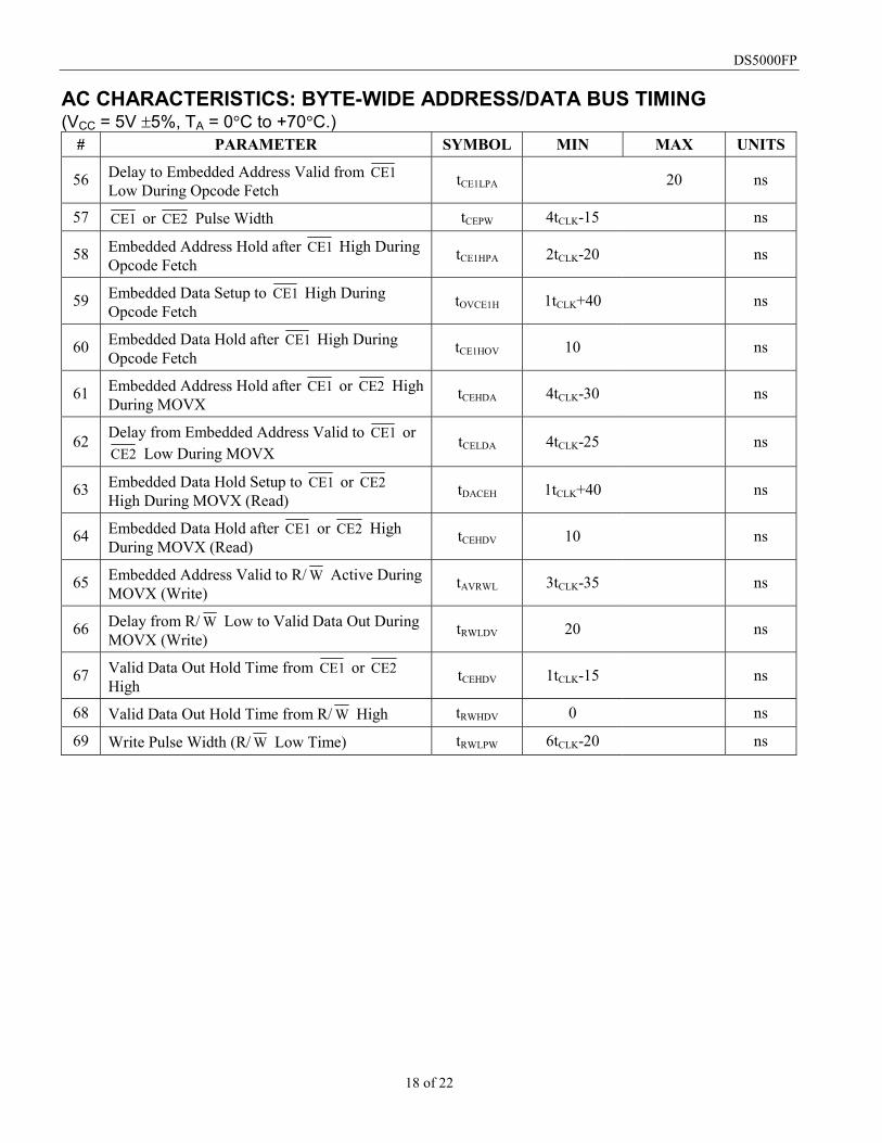
AC CHARACTERISTICS: BYTE-WIDE ADDRESS/DATA BUS TIMING (VCC = 5V �5%, TA = 0�C to +70�C.)
# PARAMETER SYMBOL MIN MAX UNITS
56 Delay to Embedded Address Valid from CE1 Low During Opcode Fetch
tCE1LPA 20 ns
57 CE1 or CE2 Pulse Width tCEPW 4tCLK-15 ns
58 Embedded Address Hold after CE1 High During Opcode Fetch
tCE1HPA 2tCLK-20 ns
59 Embedded Data Setup to CE1 High During Opcode Fetch
tOVCE1H 1tCLK+40 ns
60 Embedded Data Hold after CE1 High During Opcode Fetch
tCE1HOV 10 ns
61 Embedded Address Hold after CE1 or CE2 High During MOVX
tCEHDA 4tCLK-30 ns
62 Delay from Embedded Address Valid to CE1 or CE2 Low During MOVX
tCELDA 4tCLK-25 ns
63 Embedded Data Hold Setup to CE1 or CE2 High During MOVX (Read)
tDACEH 1tCLK+40 ns
64 Embedded Data Hold after CE1 or CE2 High During MOVX (Read)
tCEHDV 10 ns
65 Embedded Address Valid to R/ W Active During MOVX (Write)
tAVRWL 3tCLK-35 ns
66 Delay from R/ W Low to Valid Data Out During MOVX (Write)
tRWLDV 20 ns
67 Valid Data Out Hold Time from CE1 or CE2 High
tCEHDV 1tCLK-15 ns
68 Valid Data Out Hold Time from R/ W High tRWHDV 0 ns
69 Write Pulse Width (R/ W Low Time) tRWLPW 6tCLK-20 ns

DS5000FP
19 of 22
BYTE-WIDE ADDRESS/DATA BUS OPCODE FETCH CYCLE
BYTE-WIDE ADDRESS/DATA BUS OPCODE FETCH WITH DATA MEMORY READ

DS5000FP
20 of 22
BYTE-WIDE ADDRESS/DATA BUS OPCODE FETCH WITH DATA MEMORY WRITE

DS5000FP
21 of 22
PACKAGE INFORMATION (The package drawing(s) in this data sheet may not reflect the most current specifications. For the latest package outline information, go to www.maxim-ic.com/DallasPackInfo.)
56-G4005-001
MILLIMETERS DIM
MIN MAX
A - 3.15
A1 0.25 -
A2 2.55 2.87
B 0.30 0.50
C 0.13 0.23
D 23.70 24.10
D1 19.90 20.10
E 17.40 18.10
E1 13.90 14.10
E 0.80 BSC
L 0.65 0.95
DS5000FP
22 of 22
Maxim/Dallas Semiconductor cannot assume responsibility for use of any circuitry other than circuitry entirely embodied in a Maxim/Dallas Semiconductor product. No circuit patent licenses are implied. Maxim/Dallas Semiconductor reserves the right to change the circuitry and specifications without notice at any time. Maxim Integrated Products, 120 San Gabr iel Dr ive, Sunnyvale, CA 94086 408-737-7600
© 2005 Maxim Integrated Products � Printed USA
The Maxim logo is a registered trademark of Maxim Integrated Products, Inc. The Dallas logo is a registered trademark of Dallas Semiconductor Corporation.
REVISION HISTORY DATE DESCRIPTION
070605
1) Added Pb-free part to Ordering Information table. 2) Added operating voltage specification. (This is not a new specification because
operating voltage is implied in the testing limits, but rather a clarification.) 3) Updated Absolute Maximum Ratings soldering temperature to reference JEDEC
standard. 4) Added voltage rang on VCC relative to ground specification to Absolute Maximums. 5) Changed “Secure Microcontroller Data Book” references to “Secure Microcontroller
User’s Guide.”