Download - R1500x SERIES - Line One Sales
R1500x SERIES
500mA LDO REGULATOR (Operating Voltage up to 24V) NO.EA-151-130416
1
OUTLINE The R1500x series are CMOS-based positive voltage regulator (VR) ICs. The R1500xxxxB has features of high
input voltage operating, 500mA output current drive, and low supply current. A DMOS transistor is used for the driver, high voltage operating and low on resistance (0.6Ω at VOUT=10V)
device is realized. A standard regulator circuit with a current limit circuit and a thermal shutdown circuit are built in the R1500x series.
As the operating temperature range is from -40°C to 105°C and maximum input voltage is up to 24V, the R1500x series are suitable for the constant voltage source for car accessories.
The regulator output voltage is fixed in the R1500x. Output voltage accuracy is ±2.0% and output voltage range is from 3.0V to 12.0V with a step of 0.1V. The chip enable pin realizes ultra low supply current standby mode.
Since the packages for these ICs are the SOT-89-5 for high density mounting of the ICs on boards, and the TO-252-5-P2(Non-promotion). ∗) The DMOS (Double Diffused MOS) transistor adopted by R1500x is characterized by a double diffusion structure which
comprises a low density n-type (channel) diffused layer and a high density p-type (sources) diffused layer from the edge of the gate electrode. The R1500x series possess outstanding properties of high operating voltage and low on-resistance, which have been achieved by the channel length scaled down to submicron dimensions and decreased thickness of the gate oxide film.
FEATURES • Input Voltage Range ...................................................4.0V to 24.0V • Supply Current .............................................................Typ. 70μA • Standby Current ...........................................................Typ. 0.1μA • Ripple Rejaction .........................................................Typ. 60dB (VOUT=5.0V) • Temperature-Drift Coefficient of Output Voltage ..........Typ. ±100ppm/°C • Output Current..............................................................Min. 500mA (VIN=VOUT+1V) • Line Regulation ............................................................Typ. 0.05%/V • Output Voltage Accuracy..............................................±2% • Output Voltage..............................................................3.0V to 12.0V (0.1V steps) (For other voltages, please refer to MARK INFORMATIONS.) • Packages......................................................................SOT-89-5, TO-252-5-P2(Non-promotion) • Built-in Current Limit Circuit • Built-in Fold-Back Circuit • Built-in Thermal Shutdown Circuit • Operating Temperature range ......................................−40°C to 105°C
APPLICATIONS
• Power source for home appliances such as refrigerators, rice cookers, electric water warmers, etc. • Power source for car audio equipment, car navigation system, ETC system, etc. • Power source for notebook PCs, digital TVs, cordless phones, and private LAN system, etc. • Power source for office equipment machines such as copiers, printers, facsimiles, scanners, projectors, etc.
R1500x
2
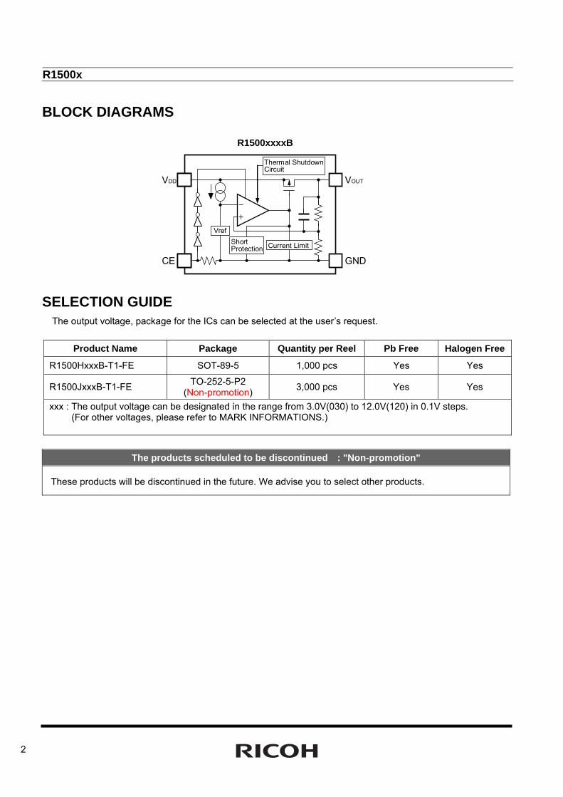
BLOCK DIAGRAMS
R1500xxxxB
VDD VOUT
CE GND
Current LimitShortProtection
Vref
Thermal ShutdownCircuit
SELECTION GUIDE The output voltage, package for the ICs can be selected at the user’s request.
Product Name Package Quantity per Reel Pb Free Halogen Free
R1500HxxxB-T1-FE SOT-89-5 1,000 pcs Yes Yes
R1500JxxxB-T1-FE TO-252-5-P2 (Non-promotion) 3,000 pcs Yes Yes
xxx : The output voltage can be designated in the range from 3.0V(030) to 12.0V(120) in 0.1V steps. (For other voltages, please refer to MARK INFORMATIONS.)
The products scheduled to be discontinued : "Non-promotion"
These products will be discontinued in the future. We advise you to select other products.
R1500x
3
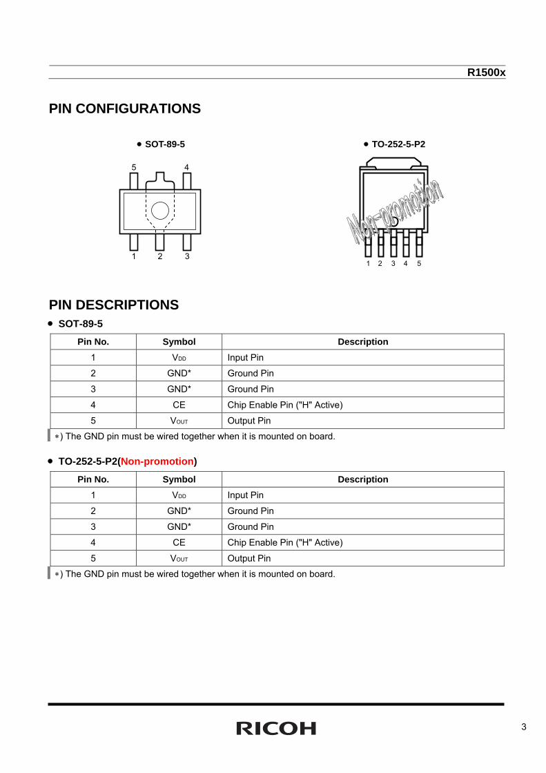
PIN CONFIGURATIONS
• SOT-89-5 • TO-252-5-P2
1 3
5 4
2
1 2 3 4 5
PIN DESCRIPTIONS • SOT-89-5
Pin No. Symbol Description 1 VDD Input Pin
2 GND* Ground Pin
3 GND* Ground Pin
4 CE Chip Enable Pin ("H" Active)
5 VOUT Output Pin
∗) The GND pin must be wired together when it is mounted on board.
• TO-252-5-P2(Non-promotion)
Pin No. Symbol Description 1 VDD Input Pin
2 GND* Ground Pin
3 GND* Ground Pin
4 CE Chip Enable Pin ("H" Active)
5 VOUT Output Pin
∗) The GND pin must be wired together when it is mounted on board.

R1500x
4
ABSOLUTE MAXIMUM RATINGS Symbol Item Rating Unit
VIN Input Voltage 36 V
VCE Input Voltage (CE Pin) −0.3 to VIN < = 36 V
VOUT Output Voltage −0.3 to VIN < = 36 V
Power Dissipation (SOT-89-5)* 900 PD
Power Dissipation (TO-252-5-P2)*(Non-promotion) 1900 mW
Topt Operating Temperature Range −40 to 105 °C
Tstg Storage Temperature Range −55 to 125 °C
∗) For Power Dissipation, please refer to PACKAGE INFORMATION.
ABSOLUTE MAXIMUM RATINGS
Electronic and mechanical stress momentarily exceeded absolute maximum ratings may cause the permanent damages and may degrade the life time and safety for both device and system using the device in the field. The functional operation at or over these absolute maximum ratings is not assured.
R1500x
5
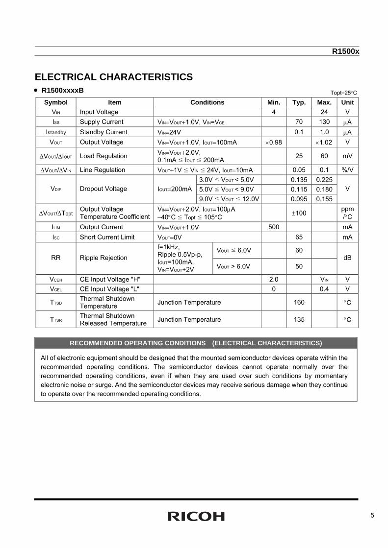
ELECTRICAL CHARACTERISTICS • R1500xxxxB Topt=25°C
Symbol Item Conditions Min. Typ. Max. UnitVIN Input Voltage 4 24 V ISS Supply Current VIN=VOUT+1.0V, VIN=VCE 70 130 μA
Istandby Standby Current VIN=24V 0.1 1.0 μA VOUT Output Voltage VIN=VOUT+1.0V, IOUT=100mA ×0.98 ×1.02 V
ΔVOUT/ΔIOUT Load Regulation VIN=VOUT+2.0V, 0.1mA < = IOUT < = 200mA 25 60 mV
ΔVOUT/ΔVIN Line Regulation VOUT+1V < = VIN < = 24V, IOUT=10mA 0.05 0.1 %/V3.0V < = VOUT < 5.0V 0.135 0.2255.0V < = VOUT < 9.0V 0.115 0.180VDIF Dropout Voltage IOUT=200mA9.0V < = VOUT < = 12.0V 0.095 0.155
V
ΔVOUT/ΔTopt Output Voltage Temperature Coefficient
VIN=VOUT+2.0V, IOUT=100μA −40°C < = Topt < = 105°C ±100 ppm
/°C ILIM Output Current VIN=VOUT+1.0V 500 mAISC Short Current Limit VOUT=0V 65 mA
VOUT < = 6.0V 60 RR Ripple Rejection
f=1kHz, Ripple 0.5Vp-p, IOUT=100mA, VIN=VOUT+2V VOUT > 6.0V 50
dB
VCEH CE Input Voltage "H" 2.0 VIN V VCEL CE Input Voltage "L" 0 0.4 V
TTSD Thermal Shutdown Temperature Junction Temperature 160 °C
TTSR Thermal Shutdown Released Temperature Junction Temperature 135 °C
RECOMMENDED OPERATING CONDITIONS (ELECTRICAL CHARACTERISTICS)
All of electronic equipment should be designed that the mounted semiconductor devices operate within the recommended operating conditions. The semiconductor devices cannot operate normally over the recommended operating conditions, even if when they are used over such conditions by momentary electronic noise or surge. And the semiconductor devices may receive serious damage when they continue to operate over the recommended operating conditions.
R1500x
6
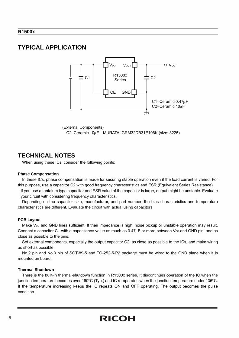
TYPICAL APPLICATION
C1 R1500x Series
VDD VOUT
CE GND
C2
VOUT
C1=Ceramic 0.47μF C2=Ceramic 10μF
(External Components) C2: Ceramic 10μF MURATA: GRM32DB31E106K (size: 3225)
TECHNICAL NOTES
When using these ICs, consider the following points:
Phase Compensation In these ICs, phase compensation is made for securing stable operation even if the load current is varied. For
this purpose, use a capacitor C2 with good frequency characteristics and ESR (Equivalent Series Resistance). If you use a tantalum type capacitor and ESR value of the capacitor is large, output might be unstable. Evaluate your circuit with considering frequency characteristics. Depending on the capacitor size, manufacturer, and part number, the bias characteristics and temperature
characteristics are different. Evaluate the circuit with actual using capacitors.
PCB Layout Make VDD and GND lines sufficient. If their impedance is high, noise pickup or unstable operation may result.
Connect a capacitor C1 with a capacitance value as much as 0.47μF or more between VDD and GND pin, and as close as possible to the pins.
Set external components, especially the output capacitor C2, as close as possible to the ICs, and make wiring as short as possible.
No.2 pin and No.3 pin of SOT-89-5 and TO-252-5-P2 package must be wired to the GND plane when it is mounted on board.
Thermal Shutdown
There is the built-in thermal-shutdown function in R1500x series. It discontinues operation of the IC when the junction temperature becomes over 160°C (Typ.) and IC re-operates when the junction temperature under 135°C. If the temperature increasing keeps the IC repeats ON and OFF operating. The output becomes the pulse condition.
R1500x
7
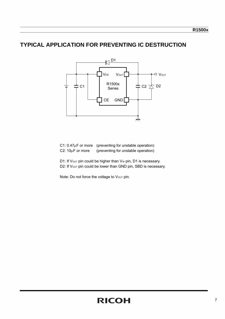
TYPICAL APPLICATION FOR PREVENTING IC DESTRUCTION
C1: 0.47μF or more (preventing for unstable operation) C2: 10μF or more (preventing for unstable operation) D1: If VOUT pin could be higher than VIN pin, D1 is necessary. D2: If VOUT pin could be lower than GND pin, SBD is necessary. Note: Do not force the voltage to VOUT pin.
C1 R1500x Series
VDD VOUT
CE GND
C2
VOUT
D1
D2
R1500x
8
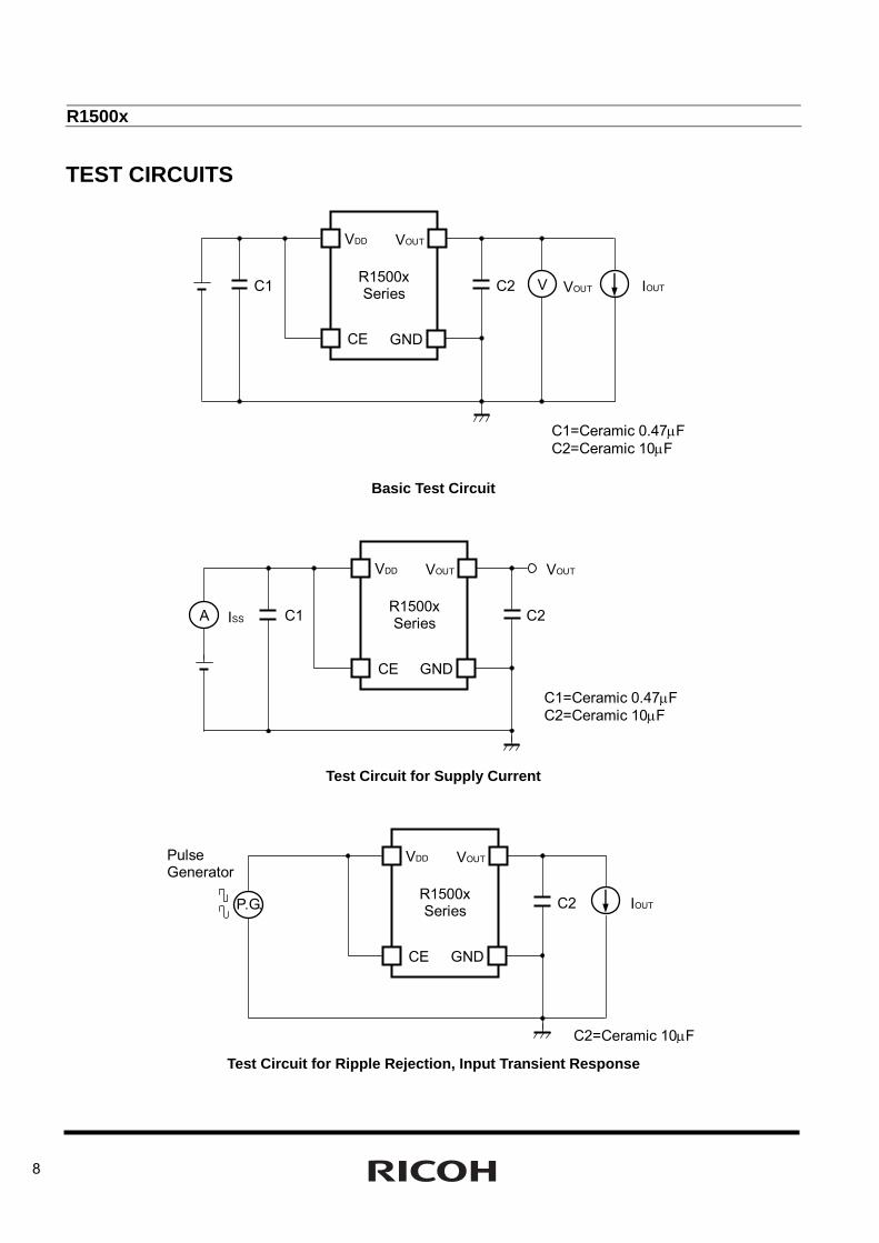
TEST CIRCUITS
C1 R1500x Series
VDD VOUT
CE GND
VC2 VOUT IOUT
C1=Ceramic 0.47μF C2=Ceramic 10μF
Basic Test Circuit
C1 R1500x Series
VDD VOUT
CE GND
C2A ISS
C1=Ceramic 0.47μF C2=Ceramic 10μF
VOUT
Test Circuit for Supply Current
R1500x Series
VDD VOUT
CE GND
C2
Pulse Generator
IOUT
C2=Ceramic 10μF
P.G.
Test Circuit for Ripple Rejection, Input Transient Response
R1500x
9
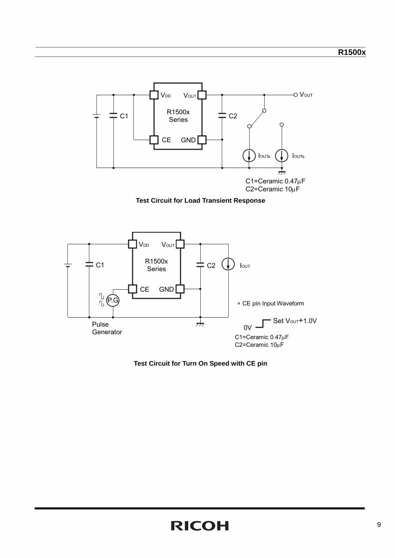
C1 R1500x Series
VDD VOUT
CE GND
C2
IOUTa IOUTb
C1=Ceramic 0.47μF C2=Ceramic 10μF
VOUT
Test Circuit for Load Transient Response
R1500x Series
VDD VOUT
CE GND
C2
Pulse Generator
IOUT
P.G.
C1
∗ CE pin Input Waveform
0VSet VOUT+1.0V
C1=Ceramic 0.47μF C2=Ceramic 10μF
Test Circuit for Turn On Speed with CE pin
R1500x
10
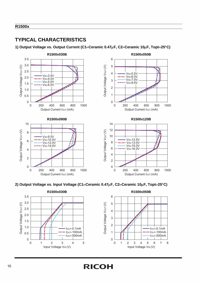
TYPICAL CHARACTERISTICS 1) Output Voltage vs. Output Current (C1=Ceramic 0.47μF, C2=Ceramic 10μF, Topt=25°C)
R1500x030B R1500x050B
0 600200 800400 1000
Output Current IOUT (mA)
Outp
ut V
oltage V
OU
T (V
)
0
3.5
2.5
2.0
1.5
3.0
1.0
0.5
VIN=3.5VVIN=4.0VVIN=5.0VVIN=6.0V
0 600200 800400 1000
Output Current IOUT (mA)
Outp
ut V
oltage V
OU
T (V
)0
6
5
4
3
2
1
VIN=5.5VVIN=6.0VVIN=7.0VVIN=9.0V
R1500x090B R1500x120B
0 600200 800400 1000
Output Current IOUT (mA)
Outp
ut V
oltage V
OU
T (V
)
0
10
8
6
4
2
VIN=9.5VVIN=10.0VVIN=12.0VVIN=14.0V
0 600200 800400 1000
Output Current IOUT (mA)
Outp
ut V
oltage V
OU
T (V
)
0
14
10
8
6
12
4
2
VIN=12.5VVIN=13.0VVIN=15.0VVIN=16.0V
2) Output Voltage vs. Input Voltage (C1=Ceramic 0.47μF, C2=Ceramic 10μF, Topt=25°C)
R1500x030B R1500x050B
0 31 42 5
Input Voltage VIN (V)
Outp
ut V
oltage V
OU
T (V
)
0
3.5
2.5
2.0
1.5
3.0
1.0
0.5
IOUT=0.1mAIOUT=100mAIOUT=500mA
0 41 62 5 73 8
Input Voltage VIN (V)
Outp
ut V
oltage V
OU
T (V
)
0
6
5
4
3
2
1
IOUT=0.1mAIOUT=100mAIOUT=500mA
R1500x
11
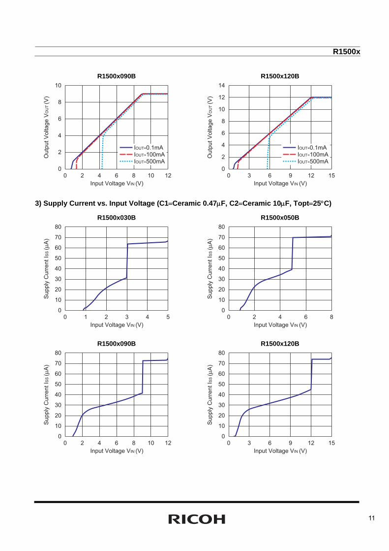
R1500x090B R1500x120B
0 82 4 106 12
Input Voltage VIN (V)
Outp
ut V
oltage V
OU
T (V
)
0
10
8
6
4
2IOUT=0.1mAIOUT=100mAIOUT=500mA
0 93 126 15
Input Voltage VIN (V)
Outp
ut V
oltage V
OU
T (V
)
0
14
10
8
6
12
4
2
IOUT=0.1mAIOUT=100mAIOUT=500mA
3) Supply Current vs. Input Voltage (C1=Ceramic 0.47μF, C2=Ceramic 10μF, Topt=25°C)
R1500x030B R1500x050B
0 31 42 5
Input Voltage VIN (V)
Supply
Curr
ent IS
S (
μA)
0
80
50
40
30
60
70
20
10
0 62 4 8
Input Voltage VIN (V)
Supply
Curr
ent IS
S (
μA)
0
80
50
40
30
60
70
20
10
R1500x090B R1500x120B
0 62 8 104 12
Input Voltage VIN (V)
Supply
Curr
ent IS
S (
μA)
0
80
50
40
30
60
70
20
10
0 93 126 15
Input Voltage VIN (V)
Supply
Curr
ent IS
S (
μA)
0
80
50
40
30
60
70
20
10
R1500x
12
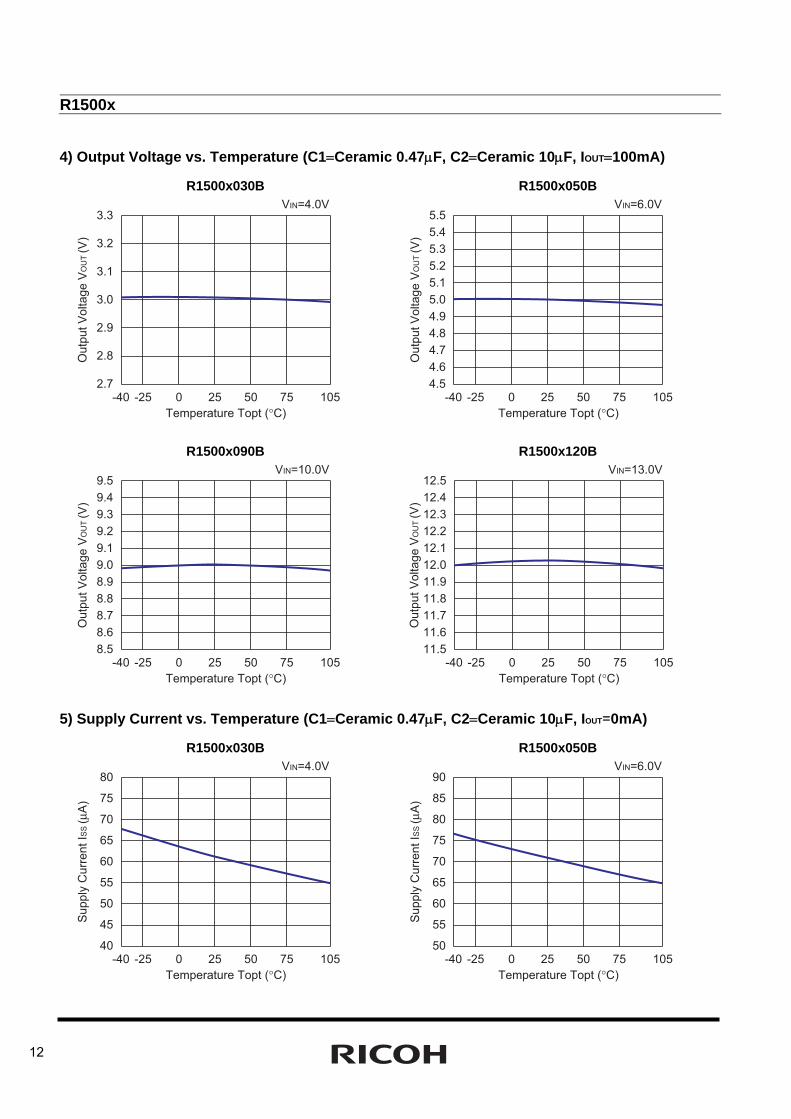
4) Output Voltage vs. Temperature (C1=Ceramic 0.47μF, C2=Ceramic 10μF, IOUT=100mA)
R1500x030B R1500x050B
-40 -25 75500 25 105
Temperature Topt (°C)
Ou
tpu
t V
olta
ge
VO
UT
(V
)
2.7
3.3
3.2
3.1
3.0
2.9
2.8
VIN=4.0V
-40 -25 75500 25 105
Temperature Topt (°C)O
utp
ut
Vo
lta
ge
VO
UT
(V
)
4.5
5.5
5.4
5.2
5.3
5.1
5.0
4.8
4.9
4.7
4.6
VIN=6.0V
R1500x090B R1500x120B
-40 -25 75500 25 105
Temperature Topt (°C)
Ou
tpu
t V
olta
ge
VO
UT
(V
)
8.5
9.5
9.4
9.2
9.0
8.8
8.6
9.3
9.1
8.9
8.7
VIN=10.0V
-40 -25 75500 25 105
Temperature Topt (°C)
Ou
tpu
t V
olta
ge
VO
UT
(V
)
11.5
12.5
12.3
12.1
11.9
11.7
12.4
12.2
12.0
11.8
11.6
VIN=13.0V
5) Supply Current vs. Temperature (C1=Ceramic 0.47μF, C2=Ceramic 10μF, IOUT=0mA)
R1500x030B R1500x050B
-40 -25 75500 25 105
Temperature Topt (°C)
Su
pp
ly C
urr
en
t IS
S (
μA)
40
80
70
60
75
65
55
50
45
VIN=4.0V
-40 -25 75500 25 105
Temperature Topt (°C)
Su
pp
ly C
urr
en
t IS
S (
μA)
50
90
80
70
85
75
65
60
55
VIN=6.0V
R1500x
13
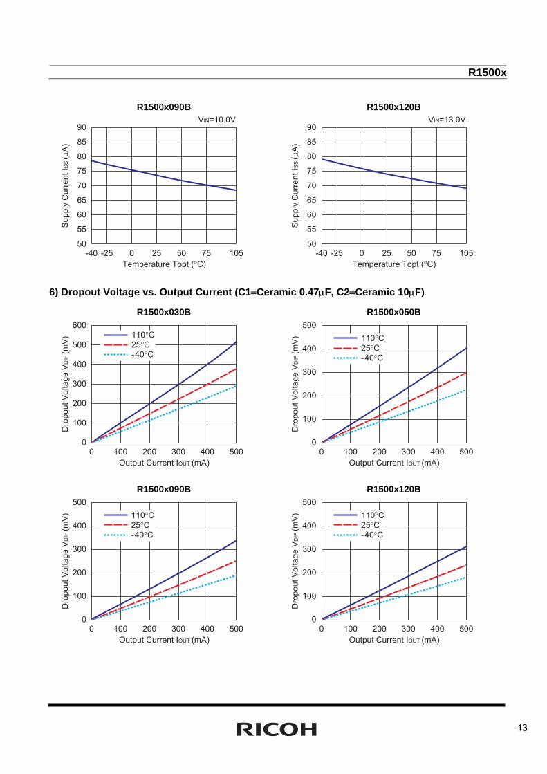
R1500x090B R1500x120B
-40 -25 75500 25 105
Temperature Topt (°C)
Su
pp
ly C
urr
en
t IS
S (
μA)
50
90
80
70
85
75
65
60
55
VIN=10.0V
-40 -25 75500 25 105
Temperature Topt (°C)
Su
pp
ly C
urr
en
t IS
S (
μA)
50
90
80
70
85
75
65
60
55
VIN=13.0V
6) Dropout Voltage vs. Output Current (C1=Ceramic 0.47μF, C2=Ceramic 10μF)
R1500x030B R1500x050B
0 300 400200100 500
Output Current IOUT (mA)
Dro
pout V
oltage V
DIF
(m
V)
0
600
500
400
300
200
100
110°C25°C-40°C
0 300 400200100 500
Output Current IOUT (mA)
Dro
pout V
oltage V
DIF
(m
V)
0
500
400
300
200
100
110°C25°C-40°C
R1500x090B R1500x120B
0 300 400200100 500
Output Current IOUT (mA)
Dro
pout V
oltage V
DIF
(m
V)
0
500
400
300
200
100
110°C25°C-40°C
0 300 400200100 500
Output Current IOUT (mA)
Dro
pout V
oltage V
DIF
(m
V)
0
500
400
300
200
100
110°C25°C-40°C
R1500x
14
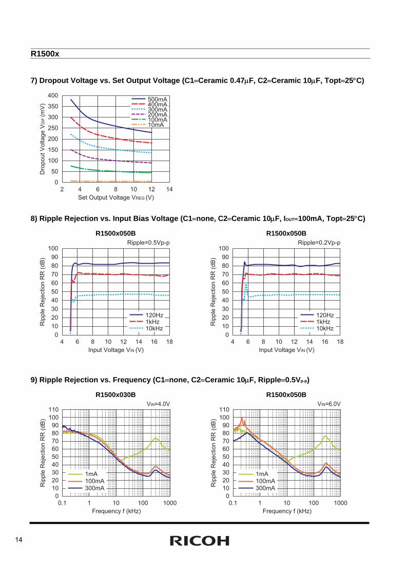
7) Dropout Voltage vs. Set Output Voltage (C1=Ceramic 0.47μF, C2=Ceramic 10μF, Topt=25°C)
2 10 12864 14
Set Output Voltage VREG (V)
Dro
pout V
oltage V
DIF
(m
V)
0
400
300
200
100
350
250
150
50
500mA400mA300mA200mA100mA10mA
8) Ripple Rejection vs. Input Bias Voltage (C1=none, C2=Ceramic 10μF, IOUT=100mA, Topt=25°C)
R1500x050B R1500x050B
4 10 1412 1686 18
Input Voltage VIN (V)
Rip
ple
Re
jectio
n R
R (
dB
)
0
100
80
60
40
20
90
70
50
30
10
120Hz1kHz10kHz
Ripple=0.5Vp-p
4 10 1412 1686 18
Input Voltage VIN (V)
Rip
ple
Re
jectio
n R
R (
dB
)
0
100
80
60
40
20
90
70
50
30
10
120Hz1kHz10kHz
Ripple=0.2Vp-p
9) Ripple Rejection vs. Frequency (C1=none, C2=Ceramic 10μF, Ripple=0.5Vp-p)
R1500x030B R1500x050B
1mA100mA300mA
0
10
20
30
110
70
40
90
50
80
100
60
VIN=4.0V
Frequency f (kHz)
Rip
ple
Re
jectio
n R
R (
dB
)
0.1 10 1001 1000
1mA100mA300mA
0
10
20
30
110
70
40
90
50
80
100
60
VIN=6.0V
Frequency f (kHz)
Rip
ple
Re
jectio
n R
R (
dB
)
0.1 10 1001 1000
R1500x
15
R1500x090B R1500x120B
1mA100mA300mA
0
10
20
30
110
70
40
90
50
80
100
60
VIN=10.0V
Frequency f (kHz)
Rip
ple
Re
jectio
n R
R (
dB
)
0.1 10 1001 1000
1mA100mA300mA
0
10
20
30
110
70
40
90
50
80
100
60
VIN=13.0V
Frequency f (kHz)
Rip
ple
Re
jectio
n R
R (
dB
)
0.1 10 1001 1000
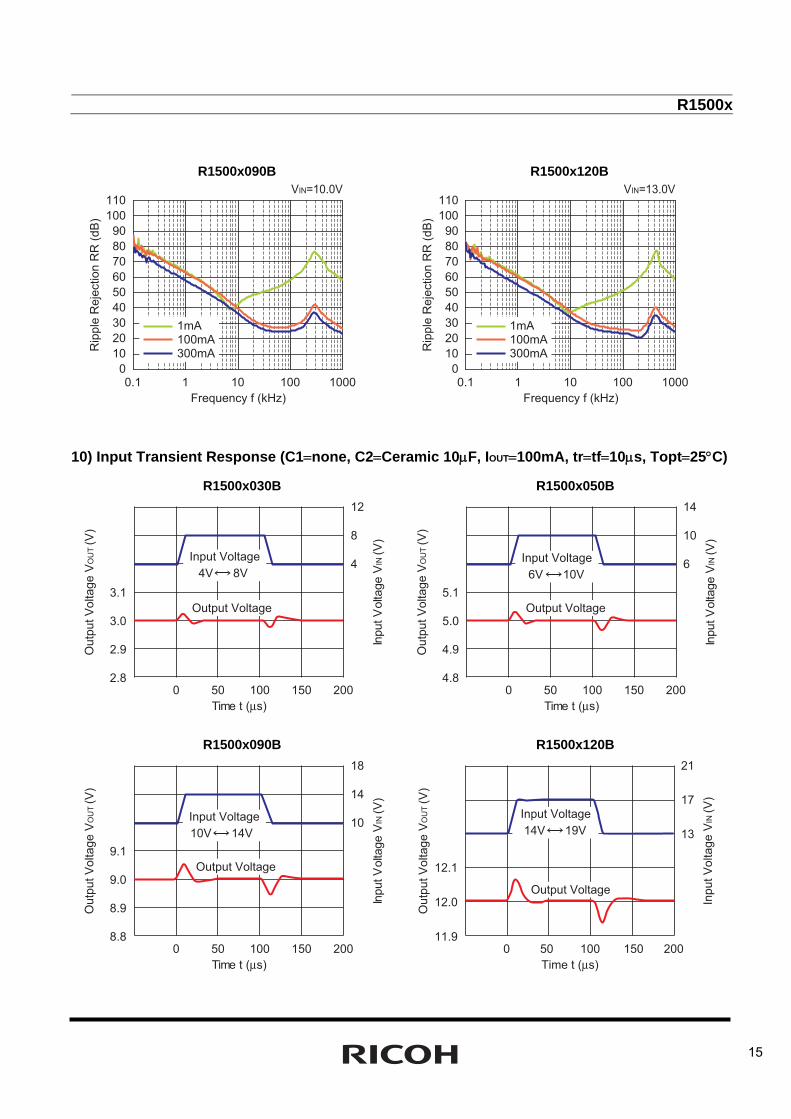
10) Input Transient Response (C1=none, C2=Ceramic 10μF, IOUT=100mA, tr=tf=10μs, Topt=25°C)
R1500x030B R1500x050B
200100 1500 50
4
8
2.8
2.9
3.0
3.1
12
Time t (μs)
Input V
olta
ge V
IN (V
)
Outp
ut V
oltage V
OU
T (V
)
Output Voltage
Input Voltage
4V 8V
200100 1500 50
6
10
4.8
4.9
5.0
5.1
14
Time t (μs)In
put V
olta
ge V
IN (V
)
Outp
ut V
oltage V
OU
T (V
)
Output Voltage
Input Voltage
6V 10V
R1500x090B R1500x120B
200100 1500 50
10
14
8.8
8.9
9.0
9.1
18
Input V
olta
ge V
IN (V
)
Outp
ut V
oltage V
OU
T (V
)
Time t (μs)
Output Voltage
Input Voltage
10V 14V
Input Voltage
14V 19V
20050 1500 100
Outp
ut V
oltage V
OU
T (V
)
Output Voltage
13
17
11.9
12.0
12.1
Input V
oltage V
IN (V
)
21
Time t (μs)
R1500x
16
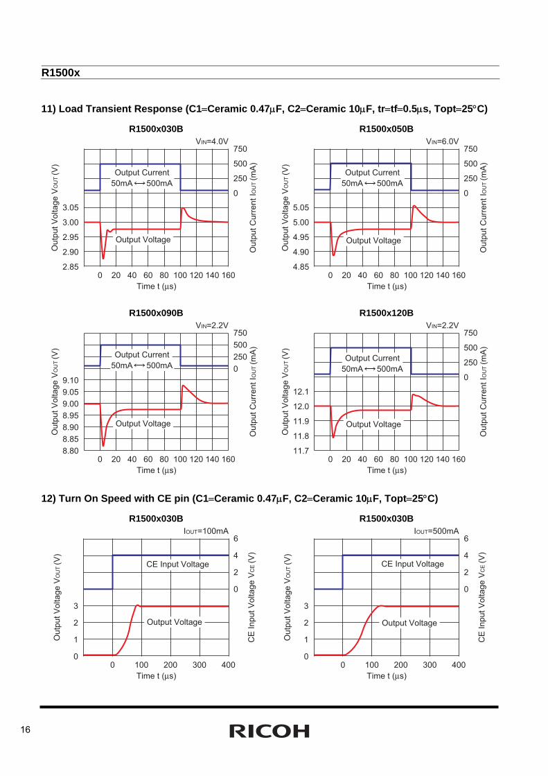
11) Load Transient Response (C1=Ceramic 0.47μF, C2=Ceramic 10μF, tr=tf=0.5μs, Topt=25°C)
R1500x030B R1500x050B
16040 1200 8060 14010020
Ou
tpu
t V
olta
ge
VO
UT
(V
)
Output Voltage
0
250
500
2.85
3.00
3.05
2.90
2.95
Ou
tpu
t C
urr
en
t IO
UT
(m
A)
750
Time t (μs)
Output Current
50mA 500mA
VIN=4.0V
16040 1200 8060 14010020
Ou
tpu
t V
olta
ge
VO
UT
(V
)
Output Voltage
0
250
500
4.85
5.00
5.05
4.90
4.95
Ou
tpu
t C
urr
en
t IO
UT
(m
A)
750
Time t (μs)
Output Current
50mA 500mA
VIN=6.0V
R1500x090B R1500x120B
16040 1200 8060 14010020
Ou
tpu
t V
olta
ge
VO
UT
(V
)
Output Voltage
0
250
500
8.80
8.95
9.10
9.05
9.00
8.85
8.90
Ou
tpu
t C
urr
en
t IO
UT
(m
A)
750
Time t (μs)
Output Current
50mA 500mA
VIN=2.2V
16040 1200 8060 14010020
Ou
tpu
t V
olta
ge
VO
UT
(V
)
Output Voltage
250
0
500
11.7
12.0
12.1
11.8
11.9
Ou
tpu
t C
urr
en
t IO
UT
(m
A)
750
Time t (μs)
Output Current
50mA 500mA
VIN=2.2V
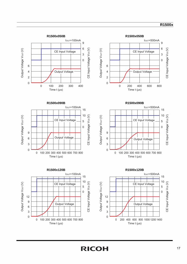
12) Turn On Speed with CE pin (C1=Ceramic 0.47μF, C2=Ceramic 10μF, Topt=25°C)
R1500x030B R1500x030B
4002000 300100
Ou
tpu
t V
olta
ge
VO
UT
(V
)
Output Voltage
2
0
4
0
3
1
2
CE
In
pu
t V
olta
ge
VC
E (V
)
6
Time t (μs)
CE Input Voltage
IOUT=100mA
4002000 300100
Ou
tpu
t V
olta
ge
VO
UT
(V
)
Output Voltage
2
0
4
0
3
1
2
CE
In
pu
t V
olta
ge
VC
E (V
)
6
Time t (μs)
CE Input Voltage
IOUT=500mA
R1500x
17
R1500x050B R1500x050B
4002000 300100
Ou
tpu
t V
olta
ge
VO
UT
(V
)
Output Voltage
3
0
6
0
6
2
4
CE
In
pu
t V
olta
ge
VC
E (V
)
9
Time t (μs)
CE Input Voltage
IOUT=100mA
8004000 600200
Ou
tpu
t V
olta
ge
VO
UT
(V
)
Output Voltage
3
0
6
0
6
2
4
CE
In
pu
t V
olta
ge
VC
E (V
)
9
Time t (μs)
CE Input Voltage
IOUT=500mA
R1500x090B R1500x090B
8004000 600200 500100 700300
Ou
tpu
t V
olta
ge
VO
UT
(V
)
Output Voltage
5
0
10
0
9
3
6
CE
In
pu
t V
olta
ge
VC
E (V
)
15
Time t (μs)
CE Input Voltage
IOUT=100mA
8004000 600200 500100 700300
Ou
tpu
t V
olta
ge
VO
UT
(V
)
Output Voltage
5
0
10
0
9
3
6
CE
In
pu
t V
olta
ge
VC
E (V
)
15
Time t (μs)
CE Input Voltage
IOUT=500mA
R1500x120B R1500x120B
8004000 600200 500100 700300
Ou
tpu
t V
olta
ge
VO
UT
(V
)
Output Voltage
5
0
10
0
9
12
3
6
CE
In
pu
t V
olta
ge
VC
E (V
)
15
Time t (μs)
CE Input Voltage
IOUT=100mA
14008000 1200400 1000200 600
Ou
tpu
t V
olta
ge
VO
UT
(V
)
Output Voltage
5
0
10
0
9
12
3
6
CE
In
pu
t V
olta
ge
VC
E (V
)
15
Time t (μs)
CE Input Voltage
IOUT=500mA
R1500x
18
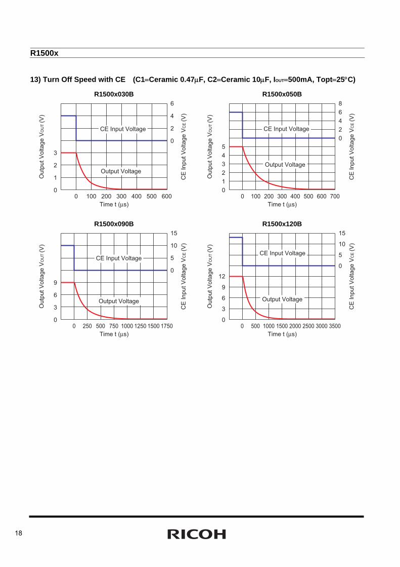
13) Turn Off Speed with CE (C1=Ceramic 0.47μF, C2=Ceramic 10μF, IOUT=500mA, Topt=25°C)
R1500x030B R1500x050B
600300 500100 4000 200
Outp
ut V
oltage V
OU
T (V
)
Output Voltage
2
0
4
0
3
1
2
CE
Input V
oltage V
CE
(V
)
6
Time t (μs)
CE Input Voltage
700300 500 600100 4000 200
Outp
ut V
oltage V
OU
T (V
)
Output Voltage
2
4
0
6
0
5
1
3
2
4
CE
Input V
oltage V
CE
(V
)
8
Time t (μs)
CE Input Voltage
R1500x090B R1500x120B
1750750 1250 1500250 10000 500
Outp
ut V
oltage V
OU
T (V
)
Output Voltage
5
10
0
0
9
3
6
CE
Input V
oltage V
CE
(V
)
15
Time t (μs)
CE Input Voltage
35001500 2500 3000500 20000 1000
Outp
ut V
oltage V
OU
T (V
)
Output Voltage
5
10
0
0
3
9
6
12
CE
Input V
oltage V
CE
(V
)
15
Time t (μs)
CE Input Voltage
R1500x
20
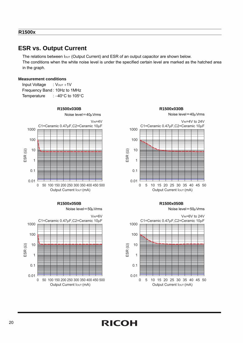
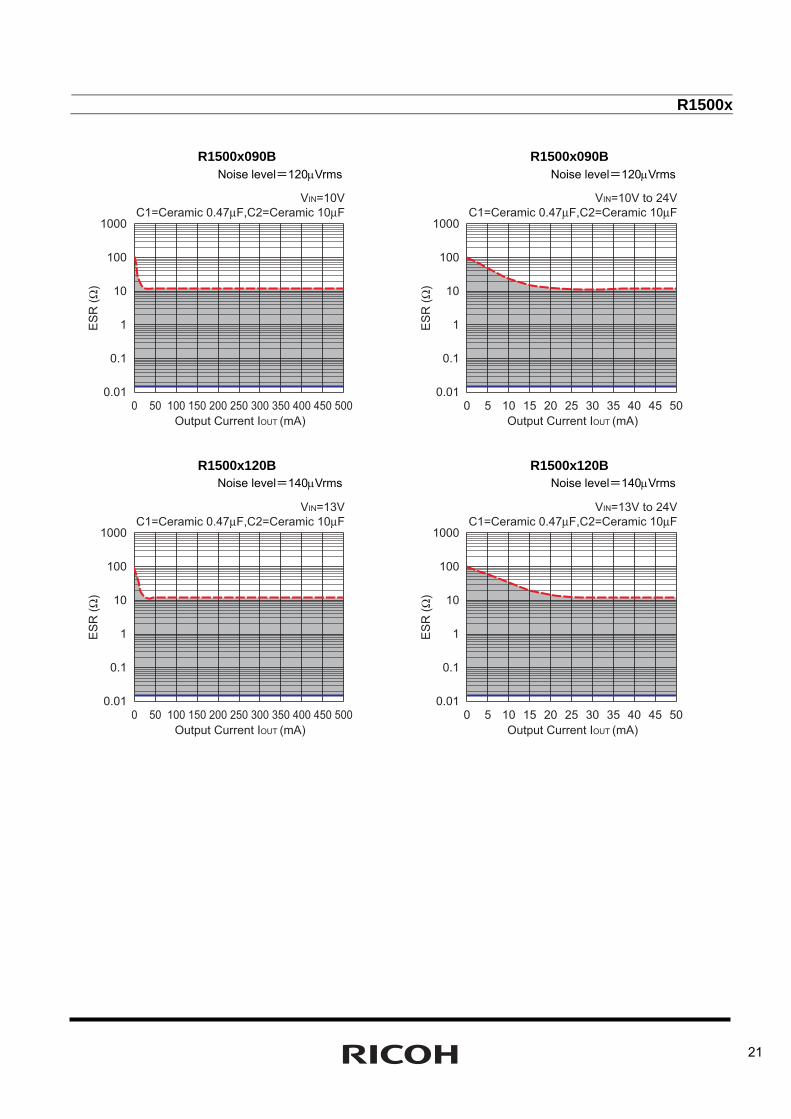
ESR vs. Output Current The relations between IOUT (Output Current) and ESR of an output capacitor are shown below. The conditions when the white noise level is under the specified certain level are marked as the hatched area in the graph.
Measurement conditions
Input Voltage : VOUT +1V Frequency Band : 10Hz to 1MHz Temperature : −40°C to 105°C
R1500x030B R1500x030B
0 100 300200 400 45050 250150 350 500
Output Current IOUT (mA)
ES
R (
Ω)
VIN=4V
C1=Ceramic 0.47μF,C2=Ceramic 10μF
0.01
1000
1
0.1
10
100
0 20 40 4510 3015 355 25 50
Output Current IOUT (mA)
ES
R (
Ω)
VIN=4V to 24V
C1=Ceramic 0.47μF,C2=Ceramic 10μF
0.01
1000
1
0.1
10
100
R1500x050B R1500x050B
0 100 300200 400 45050 250150 350 500
Output Current IOUT (mA)
ES
R (
Ω)
VIN=6V
C1=Ceramic 0.47μF,C2=Ceramic 10μF
0.01
1000
1
0.1
10
100
0 20 40 4510 3015 355 25 50
Output Current IOUT (mA)
ES
R (
Ω)
VIN=6V to 24V
C1=Ceramic 0.47μF,C2=Ceramic 10μF
0.01
1000
1
0.1
10
100
Noise level=40μVrms Noise level=40μVrms
Noise level=50μVrms Noise level=50μVrms
R1500x
21
R1500x090B R1500x090B
0 100 300200 400 45050 250150 350 500
Output Current IOUT (mA)
ES
R (
Ω)
VIN=10V
C1=Ceramic 0.47μF,C2=Ceramic 10μF
0.01
1000
1
0.1
10
100
0 20 40105 3025 4515 35 50
Output Current IOUT (mA)E
SR
(Ω
)
VIN=10V to 24V
C1=Ceramic 0.47μF,C2=Ceramic 10μF
0.01
1000
1
0.1
10
100
R1500x120B R1500x120B
0 100 300200 400 45050 250150 350 500
Output Current IOUT (mA)
ES
R (
Ω)
VIN=13V
C1=Ceramic 0.47μF,C2=Ceramic 10μF
0.01
1000
1
0.1
10
100
0 20 40 4510 3015 355 25 50
Output Current IOUT (mA)
ES
R (
Ω)
VIN=13V to 24V
C1=Ceramic 0.47μF,C2=Ceramic 10μF
0.01
1000
1
0.1
10
100
Noise level=120μVrms Noise level=120μVrms
Noise level=140μVrms Noise level=140μVrms
RICOH COMPANY, LTD.Electronic Devices Company
http://www.ricoh.com/LSI/
For the conservation of the global environment, Ricoh is advancing the decrease of the negative environmental impact material. After Apr. 1, 2006, we will ship out the lead free products only. Thus, all products that will be shipped from now on comply with RoHS Directive.Basically after Apr. 1, 2012, we will ship out the Power Management ICs of the Halogen Free products only. (Ricoh Halogen Free products are also Antimony Free.)Halogen Free
RICOH COMPANY, LTD.Electronic Devices Company Higashi-Shinagawa Office (International Sales)3-32-3, Higashi-Shinagawa, Shinagawa-ku, Tokyo 140-8655, JapanPhone: +81-3-5479-2857 Fax: +81-3-5479-0502
RICOH EUROPE (NETHERLANDS) B.V. Semiconductor Support Centre“Nieuw Kronenburg” Prof. W.H. Keesomlaan 1, 1183 DJ, Amstelveen, The Netherlands P.O.Box 114, 1180 AC AmstelveenPhone: +31-20-5474-309 Fax: +31-20-5474-791
RICOH ELECTRONIC DEVICES KOREA Co., Ltd.11 floor, Haesung 1 building, 942, Daechidong, Gangnamgu, Seoul, KoreaPhone: +82-2-2135-5700 Fax: +82-2-2135-5705
RICOH ELECTRONIC DEVICES SHANGHAI Co., Ltd.Room403, No.2 Building, 690#Bi Bo Road, Pu Dong New district, Shanghai 201203, People's Republic of ChinaPhone: +86-21-5027-3200 Fax: +86-21-5027-3299
RICOH COMPANY, LTD.Electronic Devices Company Taipei officeRoom109, 10F-1, No.51, Hengyang Rd., Taipei City, Taiwan (R.O.C.)Phone: +886-2-2313-1621/1622 Fax: +886-2-2313-1623
1. The products and the product specifications described in this document are subject to change or discontinuation of production without notice for reasons such as improvement. Therefore, before deciding to use the products, please refer to Ricoh sales representatives for the latest information thereon.
2. The materials in this document may not be copied or otherwise reproduced in whole or in part without prior written consent of Ricoh.
3. Please be sure to take any necessary formalities under relevant laws or regulations before exporting or otherwise taking out of your country the products or the technical information described herein.
4. The technical information described in this document shows typical characteristics of and example application circuits for the products. The release of such information is not to be construed as a warranty of or a grant of license under Ricoh's or any third party's intellectual property rights or any other rights.
5. The products listed in this document are intended and designed for use as general electronic components in standard applications (office equipment, telecommunication equipment, measuring instruments, consumer electronic products, amusement equipment etc.). Those customers intending to use a product in an application requiring extreme quality and reliability, for example, in a highly specific application where the failure or misoperation of the product could result in human injury or death (aircraft, spacevehicle, nuclear reactor control system, traffic control system, automotive and transportation equipment, combustion equipment, safety devices, life support system etc.) should first contact us.
6. We are making our continuous effort to improve the quality and reliability of our products, but semiconductor products are likely to fail with certain probability. In order to prevent any injury to persons or damages to property resulting from such failure, customers should be careful enough to incorporate safety measures in their design, such as redundancy feature, firecontainment feature and fail-safe feature. We do not assume any liability or responsibility for any loss or damage arising from misuse or inappropriate use of the products.
7. Anti-radiation design is not implemented in the products described in this document.8. Please contact Ricoh sales representatives should you have any questions or comments concerning the products or the technical information.


