The Berkeley common-multi-gate (BSIMMG) model is developed to meet the present and future needs of circuit designers employ-ing advanced nano field-effect transistors (nano-FETs), such as FinFETs, with a potential to extend the technology roadmap into sub-25nm region. The BSIMMG model provides maximum versa-tility regarding multi-gate device geometry, novel materials and fabrication technology without compromising the ease of use and simulation efficiency characteristic for the previous generations of BSIM compact models.
• Versatility inchoosingdouble, triple, quadrupleorcylindricalmulti-gate FET structures realized either in bulk silicon or SOI technology
• Basedonphysicalsurfacepotentialformulations,theBSIMMGmodel is continuous, symmetric, scalable and predictive over wide range of device parameters
• TheBSIMMGmodelcapturesalmostall the importantphysicalphenomena specific for nano-FETs
• Parametersfornon-siliconchanneldevicesandhigh-kmetal-gate stack structures
• AdjustablecomplexityoftheextrinsicRCnetworkandsurfacepotentialsolutiontotherequiredmodelaccuracyandsimulationefficiency
• PossibilitytoswitchbetweentheBSIMandPSPbasedchannelmobility models.
• Surfacepotentialbasedmodelwithextraelectrostaticcontrolfrom the end-gates
• Optional simplified surface potential solution for furtherimprovements of the computational efficiency
• Quantummechanicaleffects• Corner-inducedeffectivewidthreduction• Shortchanneleffectsincludingthresholdvoltageroll-off,DIBL,
sub-threshold slope effects and channel length modulation• Poly-silicongatedepletioneffects• Mobilitydegradation• Hybrid-surface-orientationmobility• Velocitysaturation• Velocityovershootwithsourceendvelocitylimit• The internal and external, bias dependent, series resistance
model• Gatetunnelingcurrent• Gateinduceddrainandsourceleakagecurrents(GIDL,GISL)• Impactionization• Non-quasi-staticeffects• Parasiticcapacitances• Junctioncapacitancesandcurrents• Temperatureeffectsandself-heating• Thermal/flicker/shotnoise• Geometryscalingandbinningofthemodelparameters
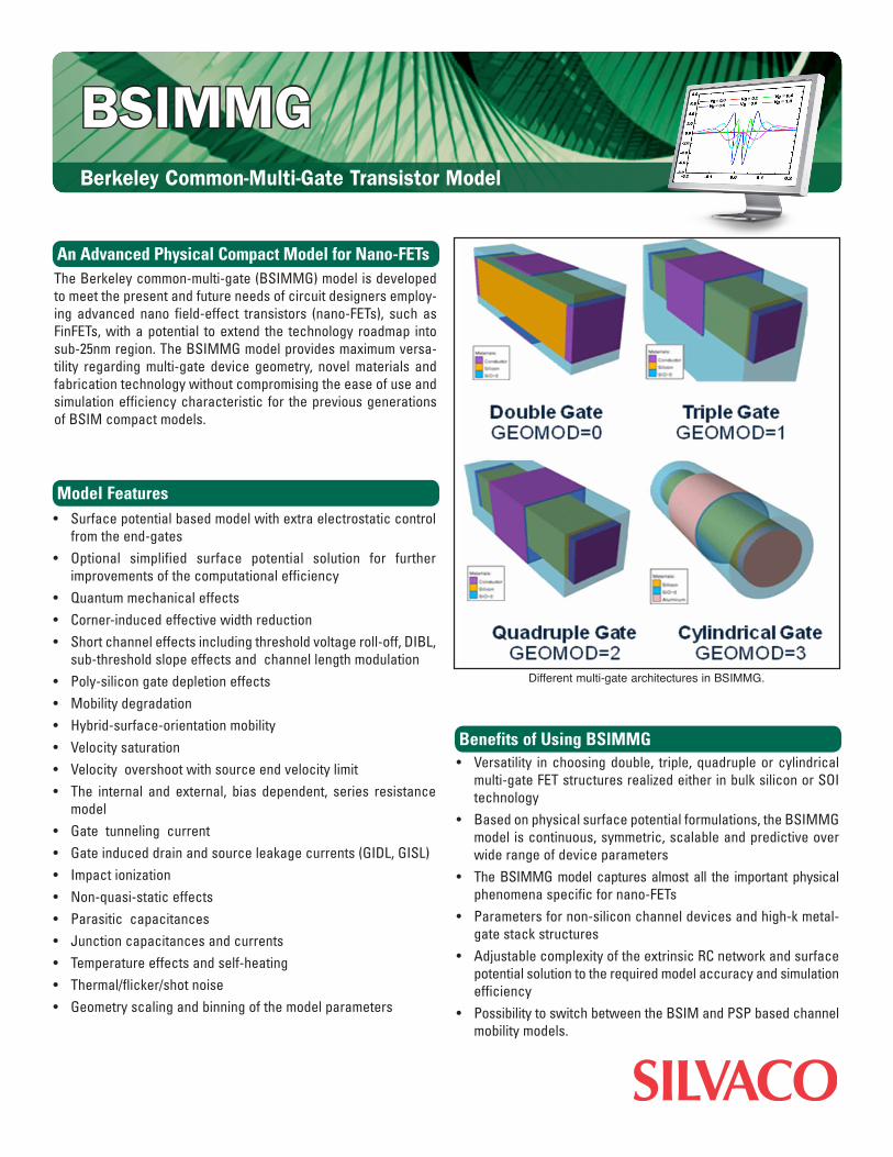
Different multi-gate architectures in BSIMMG.
BSIMMGBerkeley Common-Multi-Gate Transistor Model
An Advanced Physical Compact Model for Nano-FETs
Model Features
Benefits of Using BSIMMG

Surface potential in BSIMMG in comparison to 3-D simulation.
The third derivative of the BSIMMG drain-source current in the Gummel symmetry test for different gate voltages.
The choice of SOI or silicon bulk multi-gate technologies in BSIMMG.
Normalized capacitance from BSIMMG model (lines) and TCAD (symbols).
The transient response of the 17-stage ring oscillator test case .
1. M.V.Dunga,C.-H.Lin,M.Niknejad,andC.Hu,“BSIMMG:ACompactModel forMulti-GateTransistors” inPlanarDouble-GateTransistor,A.Amara,O.Rozeau,eds.,Springer,2009.
2. M. V.Dunga, Ph.D.Dissertation:NanoscaleCMOSModeling. UCBerkeley,2007.
3. B.Yu,H.Lu,M.Liu,andY.Taur,“Explicitcontinuousmodelsfordouble-gateandsurrounding-gateMosfets,”IEEETransactiononElectronDevices,vol.54,no.10,pp.2715–2722,October2007.
• TheBSIMMGmodelisimplementedinSmartSpiceasBSIM-CMGLevel=105-BerkeleyreleaseJune2011version105.03
• Silvaco’simplementationisfullycomplianttotheoriginalBerkeleyVerilog-AcodefortheBSIMMGmodelversion105.03.
• The node collapsing scheme is selected by combination of theBSIMMG control parameters specified in model and instance device statements
• Print, plot, save or measure the most important device internalvariables during and after simulation
• Silvaco’s implementation iscompatiblewithVZEROandBYPASSoptions and parallel architecture algorithms to achieve greater speedperformanceaswellasDCGMINoptionforimprovedcon-vergence
WWW.SILVACO.COM Rev.012014_04
References
Silvaco Implementation


