zinc stannate nanoflower (zn2sno4) photoanodes for efficient dye sensitized solar cells
TRANSCRIPT

Contents lists available at ScienceDirect
Materials Science in Semiconductor Processing
Materials Science in Semiconductor Processing ] (]]]]) ]]]–]]]
1369-80http://d
n Corrfax: þ9
E-mjerome@
Pleas10.10
journal homepage: www.elsevier.com/locate/mssp
Zinc stannate nanoflower (Zn2SnO4) photoanodes for efficientdye sensitized solar cells
M. Mary Jaculine a, C. Justin Raj b, Hee-Je Kim c, A. Jeya Rajendran d,S. Jerome Das a,n
a Department of Physics, Loyola College, Chennai 600034, Indiab Department of Chemistry, Dongguk University-Seoul, Jung-gu, Seoul, 100-715, South Koreac Department of Electrical Engineering, Pusan National University, Jangjeong-Dong, Gumjeong-Ku, Busan 609 735, South Koread Department of Chemistry, Loyola College, Chennai 600034, India
a r t i c l e i n f o
Keywords:Dye sensitized solar cellsZinc stannatePhotoanodesNanoflowersX-ray diffraction
01/$ - see front matter & 2013 Elsevier Ltd.x.doi.org/10.1016/j.mssp.2013.11.003
esponding author. Tel.: þ91 44 2817 5662;1 44 2817 5566.ail addresses: [email protected],loyolacollege.edu, [email protected] (
e cite this article as: M.M. Jaculine,16/j.mssp.2013.11.003i
a b s t r a c t
Ternary zinc stannate (Zn2SnO4) nanoparticles were synthesized using the green hydro-thermal technique at 200 1C for different reaction times and they were used as photo-anodes for dye sensitized solar cells (DSSCs). The photovoltaic performance of the DSSCcells was characterized by measuring the J–V curves in dark, and under illumination.Among the three DSSC cells, the photoanode based on Zn2SnO4 nanoflower synthesizedat 200 1C for 48 h recorded the highest conversion efficiency of 3.346% under 1 sunillumination (AM 1.5 G, 100 mW cm�2) with improved short-circuit current density of7.859 mA cm�2, and comparable open-circuit photovoltage (0.626 V) and fill factor(0.679). This enhancement of characteristics is primarily attributed to the higher currentdensity owing to its better crystalline quality as well as the larger surface area of Zn2SnO4
nanoflowers, all of which are the results of longer reaction time. The findings are furthersubstantiated by means of open-circuit photovoltage decay experiment, dye loadingbehavior and electrochemical impedance spectroscopy.
& 2013 Elsevier Ltd. All rights reserved.
1. Introduction
Energy scarcity is a global concern today. The increasinglimitedness of hydrocarbon energy is pushing up the overallcost of living which results in mass poverty and social unrest.Against this background, scientists and engineers have beenworking relentlessly to develop alternative and sustainablesources of energy especially using solar power. But despitedecades of research and developmental efforts, solar cellsare still expensive and wanting in high efficiency, making itan uncompetitive alternative to fossil fuels. One of themain reasons for the high cost of traditional semiconductor
All rights reserved.
S.J. Das).
et al., Materials Scien
photovoltaic solar cells is their poor design. In fact, the amountof energy converted from light into electricity finally dependson how many electrons that can pass across the interfacebetween the two layers. One way to increase the creativeefficiency is to create very high surface areas at the interface.The cell that could possibly achieve very high surface area atthe interface is the third generation solar cell that is known asdye-sensitized solar cell (DSSC), or Gratzel cell – named afterits inventor [1]. These cells are more flexible, and they canoperate even in low lighting conditions. Since the dye is muchlarger than the actual area of the cell, it increases the surfacearea by more than a thousand times. Therefore as an alter-native to amorphous conventional solar silicon cells, DSSCsoffer a realistic option for harvesting sunlight into electricalenergy, with appreciable high conversion efficiency alongwith other advantages of being environment friendly, easyto fabricate and economically viable [2–4].
ce in Semiconductor Processing (2013), http://dx.doi.org/
M.Mary Jaculine et al. / Materials Science in Semiconductor Processing ] (]]]]) ]]]–]]]2
In a DSSC, light is absorbed by a dye sensitizer adsorbedon the surface of a wide-band gap semiconductor. Chargeseparation takes place at the interface via photo-inducedelectrons from the lowest unoccupied molecular orbit(LUMO) of dye sensitizer into the conduction band of thesemiconductor and transported through the conductionband of the semiconductor to the external circuit [5]. Thesemiconductor oxide electrode material is a critical factordetermining the performance of DSSCs [6]. Several binarysemiconductor oxide materials have been studied in devel-oping DSSCs such as Nb2O5 [7], ZnO [8,9], SnO2 [10], WO3
[11], In2O3 [12] and TiO2 [13–16]. Among these, nanocrystal-line TiO2 and ZnO are found to be the most excellentmaterials owing to their high performance in DSSC. Besidesthese binary oxides, special attention is also paid to theternary oxides, which provide more freedom to tune thechemical properties of the material and band structure [17].To the best of our available knowledge, SrTiO3 (η¼1.8%) andZn2SnO4 (η¼3.7%) are the only two ternary oxides reportedfor DSSCs applications [18]. The most commonly usedmaterial for charge transport in DSSCs is a mesoporousnetwork of TiO2 nanoparticles, which have shown excellentphotoelectric conversion efficiency [19,20]. However therehave been research attempts in the recent times to identifynewmaterials for improving the electron transport as well asfor reducing the recombination rate which will eventuallyreplace the widely used TiO2. Zinc stannate (Zn2SnO4), beinga wide-band gap semiconductor (band gap Eg¼3.6 eV andelectron mobility of 10–15 cm2 V�1 s�1) is widely proposedas an anode material for dye-sensitized solar cells (DSSCs).Zn2SnO4 is particularly interesting because of its physical andelectrical properties while also possessing good chemical,thermal stability and low visible absorption. Because of theirlarge band gap (3.6 eV), Zn2SnO4 cells could have greaterphotostability against UV light than TiO2 [18]. Further theelectron lifetime is proven to be larger for Zn2SnO4 than forTiO2 [18]. Zn2SnO4 also shows dramatically reduced acidetching rate in comparison with ZnO [17]. The above statedfacts have been confirmed by several research results. Avileset al. [18] reported that Zn2SnO4 is an interesting material fordye-sensitized photoanodes since the large band to bandtransition substantially diminishes photo-bleaching and pre-sents a lower electron-triiodide recombination rate. Villarrealin his study concluded the position of the conduction band(CB) for Zn2SnO4 located at higher energy level than for TiO2,which tends to transport photo injected electrons muchfaster [21]. In this work, we have demonstrated the photo-voltaic performance of DSSCs fabricated using the samplessynthesized with green hydrothermal technique at 200 1Cfor different reaction times. Further dye loading behavior andcharge transfer kinetics were analyzed using UV–vis spectralanalysis and electrochemical impedance spectroscopy (EIS).
2. Experimental details
2.1. Synthesis of Zn2SnO4 nanoparticles
All reagents were of analytical grade purchased fromMerck and used as received without further purification. Zincchloride (ZnCl2) and tin chloride dihydrate (SnCl2 �2H2O)were used as precursors and NaOH as the mineralizer for the
Please cite this article as: M.M. Jaculine, et al., Materials Scien10.1016/j.mssp.2013.11.003i
hydrothermal synthesis of Zn2SnO4. The process began bydissolving SnCl2 �2H2O (3 mmol) and ZnCl2 (3 mmol) with20 mL of double distilled water separately to form twotransparent solutions. There after 20 mL of NaOH (1 M)solution was added little by little facilitated by magneticstirring into the tin chloride dihydrate transparent solution.Finally, zinc chloride solution was added drop by drop intothe above mixed solution under stirring using magneticstirrer. The mixed solution under room temperature wascontinuously stirred for 1 h until it leads to the formation ofwhite precipitate of the hybrid complex. In the end, thewhite hybrid complex was transferred into a 100 mL Teflon-lined stainless autoclave with a fill factor of approximately70%. The autoclave was sealed and maintained in a furnace at200 1C for varying time durations, in order to examine theinfluence of the reaction time on the product structure andmorphology. The autoclave was cooled naturally to roomtemperature and the precipitate thus obtained was washedseveral times in double distilled water and in absoluteethanol by repeated centrifugation and ultrasonication.Finally, the product was dried in an oven at 80 1C for 20 h.
2.2. Fabrication of Zn2SnO4 photoanodes
The photoanode was deposited on FTO (fluor-dopedSnO2 glass) glass substrate by adopting doctor bladingtechnique. The paste was prepared by adding as synthe-sized 0.5 g Zn2SnO4 nanopowder to 3 mL of an ethanol–water mixture (3:1) with 0.08 g of ethylene cellulose,0.5 mL of acetyl acetone and 1 mL of Triton X-100 solutionas surfactant. The mixture was ground thoroughly by ballmilling for 30 min under 500 rpm followed by an ultra-sonication for 1 h and made into a paste by optimizeddrying condition. The resultant paste was doctor bladed(area¼0.25 cm2) over ultrasonically cleaned FTO substrateand was sintered at 450 1C for 30 min. The thicknesses ofthe films were found to be about 15 mm and were used forthe fabrication of DSSCs.
2.3. Fabrication of DSSCs
The photoelectrodes were soaked in a 0.2 mM N719 dye(cis–bis (isothiocyanato) bis (2, 20-bipyridyl-4, 40-discar-boxylato)-ruthenium (II)-bis-tetrabutylammonium, RuC58H86N8O8S2) solution for overnight in ambient temperatureand the excess dye was removed by soaking the photo-anode in 99.9% ethanol. Platinum counter electrodes weredeposited from a commercial platinum paste (Solaronix,platinum catalyst T/SP) on a FTO glass substrate, whichwas subsequently heat treated at 400 1C for 30 min in air.Finally, the photoanodes and the counter electrodes weresealed together using a 25 mm hot-melt sealing sheet(SX 1170-25, Solaronix) and the internal space was filledwith a redox liquid electrolyte of 0.5 M LiI, 0.05 M I2 and0.5 M 4-tertbutylpyridine in acetonitrile.
2.4. Characterization
Phase formation of synthesized samples was identifiedby using SEIFERT JSO DEBYEFLEX 2002, Germany makeX-ray diffractometer with CuKα radiation (λ¼1.540598 Å)
ce in Semiconductor Processing (2013), http://dx.doi.org/

M.Mary Jaculine et al. / Materials Science in Semiconductor Processing ] (]]]]) ]]]–]]] 3
operated at 40 kV and 30 mA in the 2θ range 10–701.Morphologies were characterized by FEI Quanta FEG200-High Resolution Scanning Electron microscope(HRSEM). The current–voltage characteristics of the DSSCswere performed under 1 sun illumination (AM 1.5 G,100 mW cm�2) using San Ei Electric (XEX 301S, Japan)solar simulator having the irradiance uniformity of 73%.The amounts of dye adsorbed on the photoelectrodes werestudied using a OPTIZEN 3220 UV spectrophotometer.Electrochemical impedance spectroscopy (EIS) was
Fig. 1. XRD patterns of Zn2SnO4 synthesized nanoparticles at 200 1C fordifferent reaction times.
Fig. 2. SEM image of Zn2SnO4 synthesized nanoparticles at 200 1C for differentimage of 48 h electrode.
Please cite this article as: M.M. Jaculine, et al., Materials Scien10.1016/j.mssp.2013.11.003i
performed using a BioLogic potentiostat/galvanostat/EISanalyzer (SP-150, France).
3. Results and discussion
Fig. 1 shows the X-ray diffraction patterns of synthe-sized Zn2SnO4 nanoparticles at 200 1C for different reac-tion times. The figure shows typical peak patterns, whichcan be indexed as the Zn2SnO4 cubic structure in thestandard data (JCPDS, 24-1470). Besides the cubic phaseof Zn2SnO4 another secondary phase of ZnSnO3 (JCPDS,28-1486) was also observed in the XRD pattern. Crystallinesize was estimated from the XRD peaks of Zn2SnO4
nanoparticles using the Scherrer formula (Φ¼kλ/β cos θ)applied to the prominent peaks corresponding to the plane(311). The estimated average crystalline size of the samplessynthesized at 24 and 48 h was about 34 nm and it was27 nm for 12 h. The diffraction peak intensities corre-sponding to the plane (311) of the synthesized samplesfor the reaction times of 12, 24 and 48 h were found to be29.92, 50.43 and 48.99 respectively, whereas the intensi-ties of (440) peaks were observed as 12.77, 20.98 and40.80. The above observations demonstrate significantimprovement in crystallinity of the product with increasingreaction time. However, longer reaction time enhances thephase formation, but there still existed small amount ofZnSnO3 phase. Since, in the initial stage of the hydrothermalreaction, some complex formations such as Sn OHð Þ62� ,ZnSn OHð Þ6 and Zn OHð Þ42� are formed in the presence ofNaOH. Further, high temperature and high pressure ofhydrothermal treatment lead to the decomposition of thesecomplex formations into Zn2SnO4 nanoparticles [22].
reaction times (a) 12 h, (b) 24 h, (c) 48 h and (d) the cross sectional SEM
ce in Semiconductor Processing (2013), http://dx.doi.org/

Fig. 3. TEM images of Zn2SnO4 synthesized nanoparticles at 200 1C fordifferent reaction times (a) 12 h, (b) 24 h and (c) 48 h.
M.Mary Jaculine et al. / Materials Science in Semiconductor Processing ] (]]]]) ]]]–]]]4
However, the exact growth mechanism is not clear and needsfurther investigation.
Fig. 2a, b and c shows the scanning electron micro-graphs (SEM) of Zn2SnO4 synthesized for various reactiontimes 12 h, 24 h and 48 h respectively at 200 1C. The insetfigures show high magnification image of the samples. Theimage of the sample at 12 h reaction time shows a largeagglomeration of nanoparticles with undistinguishablemorphology. It started showing a distinct morphologywith the increase in the reaction time of the sample(nanoflowers). The sample synthesized at 24 h showedthe formation of flower like morphology. Further on, anexcellent nanoflower morphology was accomplished at areaction time of 48 h. Comparative analysis of the results(12 h and 48 h) would confirm the enhancement of welldefined morphological crystallites in the 48 h sample witha vibrant flower morphology that resembles a bunch ofroses with an average petal thickness of �95 nm. Fig. 2dshows the obtained cross-sectional view of the DSSCphotoanode with a thickness of about 15 mm.
The morphology and structure of the Zn2SnO4 nano-particles synthesized for different reaction times at 200 1Cwere further investigated by TEM analysis. Fig. 3a, b–cshows the resultant TEM images of the samples. Fromthese images it is clear that morphologies of the sampleschange from an irregular agglomerated shape (12 h) to awell defined flower like morphology (48 h) and they are ingood agreement with those observed in the SEM images.The 48 h sample TEM image demonstrates that the flower-like nanostructures are composed of nanosheets andnanoneedles as shown in Fig. 3c. It is clearly evident fromthe image that each nanosheet was composed of severalsharp nanoneedles on the surface which can provide largesurface area for the sample.
The photovoltaic performance of three Zn2SnO4 basedDSSCs was studied by measuring the photocurrent den-sity–voltage (J–V) curves both in dark and under a simu-lated illumination with a light intensity of 100 mW cm�2
(AM¼1.5). Fig. 4a shows J–V characteristics of the threecells sensitized by N719 dye. The relevant photovoltaicparameters are summarized in Table 1. The results demon-strate noticeable increase in current density and decreasein open circuit voltage as the reaction time of the synthe-sized samples keeps increasing. The short circuit currentdensity (Jsc) value increases from 6.253 mA cm�2 to7.859 mA cm�2 as the reaction time of the synthesizedsamples increases and their corresponding open circuitvoltage (Voc) decreases from 0.687 to 0.626 V. Fig. 4bpresents the power versus voltage curves for the DSSCcells prepared with the samples synthesized at 200 1C forvarious reaction times. The power output responses keepincreasing with the increase in reaction times. The lightharvesting efficiency of the DSSC with the sample synthe-sized at the reaction time of 48 h recorded enhancementowing to the maximum power output. Experimentalresults showed that the photoanode prepared with samplesynthesized at reaction time of 48 h had significantlyhigher short-circuit photocurrent (Jsc¼7.859 mA cm�2)with maximum efficiency of �3.346% as compared tothe photoanodes with the reaction times of 12 h and24 h. It indicates that the photovoltaic performance of
Please cite this article as: M.M. Jaculine, et al., Materials Scien10.1016/j.mssp.2013.11.003i
the DSSCs is dependent on the reaction time of thesynthesizing conditions as well as their improved crystal-line nature and morphology with large surface area.Also, the photocurrent generated by a DSSC is directly
ce in Semiconductor Processing (2013), http://dx.doi.org/

Fig. 4. (a) Photocurrent density–voltage (J–V) curves and (b) Powerversus voltage plot of DSSCs with Zn2SnO4 nanoparticles synthesized at200 1C for different reaction times.
Table 1Photovoltaic and EIS parameters of the Zn2SnO4 based DSSCs.
Parameters 12 h 24 h 48 h
Voc (V) 0.687 0.639 0.626Jsc (mA cm�2) 6.253 6.849 7.859FF 0.6 0.691 0.679η (%) 2.597 3.0702 3.346Rs (Ω) 14.8 17.5 17.7RCE (Ω) 46.9 46.7 48.3Rct (Ω) 134.6 76.12 74.96Cm (F) 0.00018 0.00042 0.00063
Fig. 5. Typical UV–vis absorption spectra of the desorbed dye (N719)from DSSC photoanodes based on Zn2SnO4 nanoparticles synthesized at200 1C for different reaction times.
M.Mary Jaculine et al. / Materials Science in Semiconductor Processing ] (]]]]) ]]]–]]] 5
related to the number of dye molecules that are adsorbedon the Zn2SnO4 electrode. Therefore, the greater the sur-face area, the larger the amount of photocurrent producedby the Zn2SnO4 based DSSC, hence enhancement of lightharvesting efficiency.
To validate this, the amount of dye adsorbed on thephotoanodes was fully desorbed using a 0.1 M NaOHsolution and their absorption spectra were recorded usingUV–vis spectrometer. Fig. 5 shows the amount of dyeadsorbed in the Zn2SnO4 photoanodes. The photoanodesmade with the sample which is synthesized at 48 h reaction
Please cite this article as: M.M. Jaculine, et al., Materials Scien10.1016/j.mssp.2013.11.003i
time showed the highest dye loading behavior than theother photoanodes. This enhanced dye loading behavior isattributed to its morphological change as nanosheets andnanoneedles. Further, the dye loading behavior of the 12 hsample was better than that of the 24 h sample which mightbe due to its small crystalline size. Higher current densityand efficiency resulting in enhanced loading of the innova-tive photoanode that facilitates higher density of photogen-erated electrons might be attributed to higher amount ofadsorbed dye, due to large surface area of the Zn2SnO4
nanoflowers [23,24].The cause for decrease in Voc of higher reaction time
samples is explained with the increase in dark current andthe shift in onset potential. During the transportation ofelectrons from the conduction band of the Zn2SnO4 semi-conductor to the external circuit, electrons recombine withI3�at the Zn2SnO4 surface known as dark current, resulting
in lowering of the photovoltaic performance of DSSCs. Therecombination reaction is represented as I3
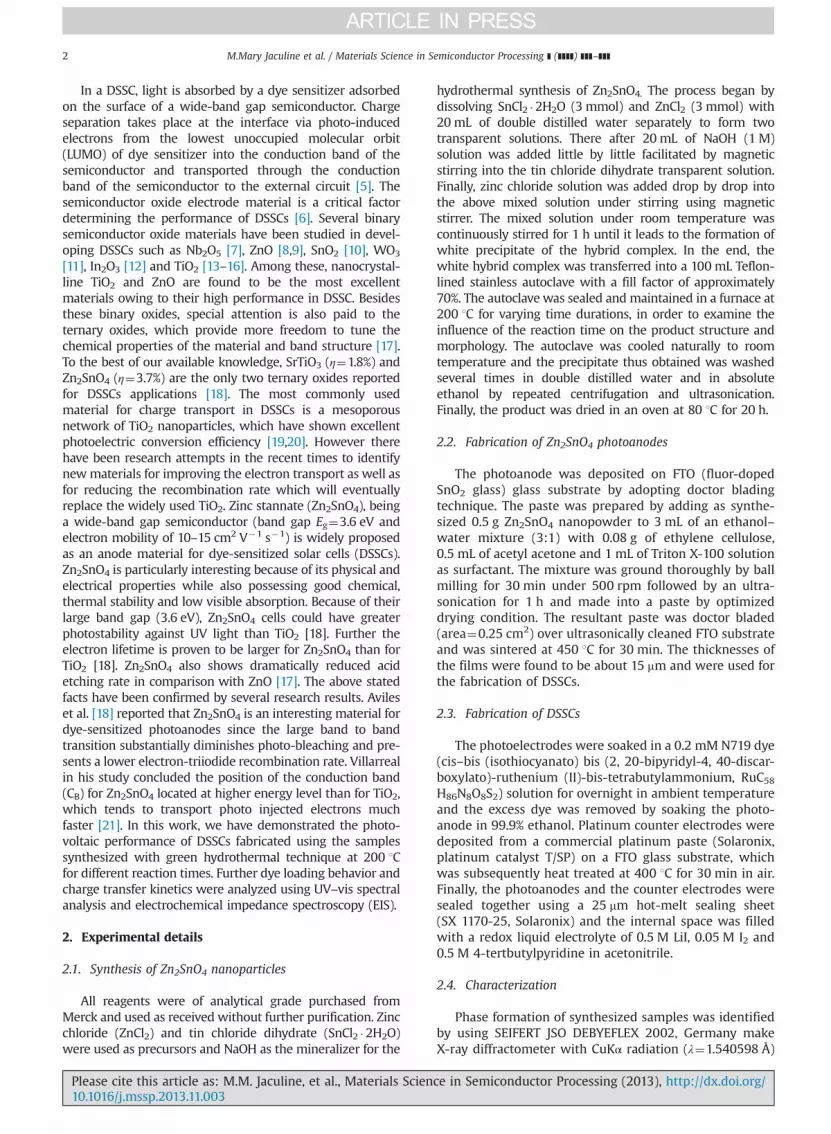
�þ2e�-3I� .Fig. 6a presents the dark current responses of the three
cells synthesized at various reaction times at temperature200 1C. Highest dark current response was observed forthe sample synthesized at 48 h resulting in the increase ofcharge recombination that lowers the open circuit voltageand hinders further improvement of cell performance [25].Fig. 6b depicts the photovoltage decay curves after turningoff the illumination for the DSSCs based on Zn2SnO4
nanoparticles synthesized at 200 1C for the reaction timesof 12, 24 and 48 h. Liu et al. [26] reported that the decay ofphotovoltage reflects the decrease of electron density inthe conduction band of the semiconducting oxide mate-rial, which is mainly caused by the charge recombinationoccurring at FTO/electrolyte and oxide/electrolyte inter-faces. In the high voltage region all the DSSCs exhibitsimilar decay trends of Voc, while the DSSC with samplesynthesized at 12 h reaction time has slow decay trend incomparison with the other DSSC cells in the middle andlow Voc regions. It indicates that the recombination pro-cess is slow, causing decrease of the charge recombinationrate at the oxide/electrolyte interface which is responsible
ce in Semiconductor Processing (2013), http://dx.doi.org/
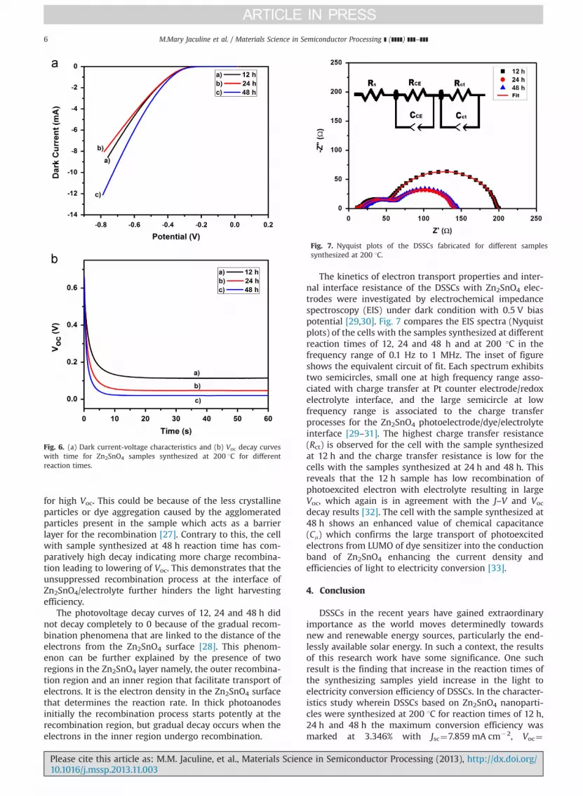
Fig. 6. (a) Dark current-voltage characteristics and (b) Voc decay curveswith time for Zn2SnO4 samples synthesized at 200 1C for differentreaction times.
Fig. 7. Nyquist plots of the DSSCs fabricated for different samplessynthesized at 200 1C.
M.Mary Jaculine et al. / Materials Science in Semiconductor Processing ] (]]]]) ]]]–]]]6
for high Voc. This could be because of the less crystallineparticles or dye aggregation caused by the agglomeratedparticles present in the sample which acts as a barrierlayer for the recombination [27]. Contrary to this, the cellwith sample synthesized at 48 h reaction time has com-paratively high decay indicating more charge recombina-tion leading to lowering of Voc. This demonstrates that theunsuppressed recombination process at the interface ofZn2SnO4/electrolyte further hinders the light harvestingefficiency.
The photovoltage decay curves of 12, 24 and 48 h didnot decay completely to 0 because of the gradual recom-bination phenomena that are linked to the distance of theelectrons from the Zn2SnO4 surface [28]. This phenom-enon can be further explained by the presence of tworegions in the Zn2SnO4 layer namely, the outer recombina-tion region and an inner region that facilitate transport ofelectrons. It is the electron density in the Zn2SnO4 surfacethat determines the reaction rate. In thick photoanodesinitially the recombination process starts potently at therecombination region, but gradual decay occurs when theelectrons in the inner region undergo recombination.
Please cite this article as: M.M. Jaculine, et al., Materials Scien10.1016/j.mssp.2013.11.003i
The kinetics of electron transport properties and inter-nal interface resistance of the DSSCs with Zn2SnO4 elec-trodes were investigated by electrochemical impedancespectroscopy (EIS) under dark condition with 0.5 V biaspotential [29,30]. Fig. 7 compares the EIS spectra (Nyquistplots) of the cells with the samples synthesized at differentreaction times of 12, 24 and 48 h and at 200 °C in thefrequency range of 0.1 Hz to 1 MHz. The inset of figureshows the equivalent circuit of fit. Each spectrum exhibitstwo semicircles, small one at high frequency range asso-ciated with charge transfer at Pt counter electrode/redoxelectrolyte interface, and the large semicircle at lowfrequency range is associated to the charge transferprocesses for the Zn2SnO4 photoelectrode/dye/electrolyteinterface [29–31]. The highest charge transfer resistance(Rct) is observed for the cell with the sample synthesizedat 12 h and the charge transfer resistance is low for thecells with the samples synthesized at 24 h and 48 h. Thisreveals that the 12 h sample has low recombination ofphotoexcited electron with electrolyte resulting in largeVoc, which again is in agreement with the J–V and Voc
decay results [32]. The cell with the sample synthesized at48 h shows an enhanced value of chemical capacitance(Cm) which confirms the large transport of photoexcitedelectrons from LUMO of dye sensitizer into the conductionband of Zn2SnO4 enhancing the current density andefficiencies of light to electricity conversion [33].
4. Conclusion
DSSCs in the recent years have gained extraordinaryimportance as the world moves determinedly towardsnew and renewable energy sources, particularly the end-lessly available solar energy. In such a context, the resultsof this research work have some significance. One suchresult is the finding that increase in the reaction times ofthe synthesizing samples yield increase in the light toelectricity conversion efficiency of DSSCs. In the character-istics study wherein DSSCs based on Zn2SnO4 nanoparti-cles were synthesized at 200 1C for reaction times of 12 h,24 h and 48 h the maximum conversion efficiency wasmarked at 3.346% with Jsc¼7.859 mA cm�2, Voc¼
ce in Semiconductor Processing (2013), http://dx.doi.org/

M.Mary Jaculine et al. / Materials Science in Semiconductor Processing ] (]]]]) ]]]–]]] 7
0.626 V and FF¼0.679. Furthermore, dark current response,open circuit voltage decay and electrochemical impedancespectra (EIS) results which were attained in the processindicated higher recombination rate of the injected electronswith the electrolyte and fast injection of electrons from LUMOof dye sensitizer into Zn2SnO4 photoanodes. The scope forachieving further efficiency levels is possible if the chargerecombinations could be minimized. The field is wide openfor further research and promising results.
Acknowledgments
The corresponding author (SJD) gratefully acknowledgeBRNS (Board of Research in Nuclear Sciences – Govern-ment of India, Project no. 2008/37/1/BRNS/1513) for pro-viding financial assistance from which the lab wasdeveloped. They are also thankful to Dr. J. Mary Linet andMs. J.P. Angelina, Assistant Professors of Physics, LoyolaCollege for their valuable suggestions.
References
[1] B. O’Regan, M. Gratzel, Nature 353 (1991) 737–740.[2] H. Tributsch, Coord. Chem. Rev. 248 (2004) 1511–1530.[3] P.V. Kamat, Meeting the Clean Energy Demand: Nanostructure
Architectures for Solar Energy Conversion, J. Phys. Chem. C 111(2007) 2834–2860.
[4] H.N. Kim, J.H. Moon, Curr. Appl. Phys. 13 (2013) 841–845.[5] J.Y. Kim, Y.H. Kim, Y.S. Kim, Curr. Appl. Phys. 11 (2013) S117–S121.[6] C. Justin Raj, S.N. Karthick, K.V. Hemalatha, M.K. Son, H.J Kim,
K. Prabakar, J. Sol–Gel Sci. Technol. 62 (2012) 453–459.[7] K. Sayama, H. Sugihara, H. Arakawa, Chem. Mater. 10 (1998)
3825–3832.[8] S. Rani, P. Suri, P.K. Shishodia, R.M. Mehra, Sol. Energy Mater. Sol.
Cells 92 (2008) 1639–1645.[9] C.H. Chao, C.H. Chan, J.J. Huang, L.S. Chang, H.C. Shih, Curr. Appl.
Phys. 11 (2013) S136–S139.
Please cite this article as: M.M. Jaculine, et al., Materials Scien10.1016/j.mssp.2013.11.003i
[10] A. Kay, M. Gratzel, Chem. Mater. 14 (2002) 2930–2935.[11] H. Zheng, Y. Tachibana, K. Kalantar-Zadeh, Langmuir 26 (2010)
19148–19152.[12] S. Mori, A. Asano, J. Phys. Chem. C 114 (2010) 13113–13117.[13] M.R. Mohammadi, R.R.M. Louca, D.J. Fray, M.E. Welland, Sol. Energy
86 (2012) 2654–2664.[14] S.H. Kang, W. Lee, Y.C. Nah, K.S. Lee, H.S. Kim, Curr. Appl. Phys. 13
(2013) 252–255.[15] J. Lee, K.S. Hong, K. Shin, J.Y. Jho, J. Ind. Eng. Chem. 18 (2012) 19–23.[16] J. Nayak, K. Prabakar, J.W. Park, H. Kim, Electrochim. Acta 65 (2012)
44–49.[17] B. Tan, E. Toman, Y. Li, Y. Wu, J. Am. Chem. Soc. 129 (2007)
4162–4163.[18] M.A.A. Aviles, Y. Wu, J. Am. Chem. Soc. 131 (2009) 3216–3224.[19] V. Thavasi, V. Renugopalakrishnan, R. Jose, S. Ramakrishna, Mater.
Sci. Eng. R 63 (2009) 81–99.[20] M. Nazeeruddin, S. Fantacci, A. Selloni, G. Viscardi, P. Liska, S. Ito,
B. Takeru, M. Gratzel, J. Am. Chem. Soc. 127 (2005) 16835–16847.[21] T.L. Villarreal, G. Boschloo, A. Hagfeldt, J. Phys. Chem. C 111 (2007)
5549–5556.[22] A.A. Firooz, A. Mahjoub, A.A. Khodadadi, M. Movahedi, Chem. Eng.
J. 165 (2010) 735–739.[23] A. Annamalai, Y.D. Eo, C. Im, M.J. Lee, Mater. Charact 62 (2011)
1007–1015.[24] P. Teesetssopon, S. Kumar, J. Dutta, Int. J. Electrochem. Sci. 7 (2012)
4988–4999.[25] J.N. Palomares, S.A. Clifford, T. Haque, Lutz, J.R. Durrant, Chem.
Commun. 14 (2002) 1464–1465.[26] Y. Liu, X. Sun, Q. Tai, H. Hu, B. Chen, N. Huang, B. Sebo, X.Z. Zhao,
J. Alloys Compds. 509 (2011) 9264–9270.[27] S. Wu, H. Han, Q. Tai, J. Zhang, S. Xu, C. Zhou, Y. Yang, H. Hu, B. Chen,
B. Sebo, X.-Zhong Zhao, Nanotechnology 19 (2008) 215704–215709.[28] S. Chappel, L. Grinis, A. Ofir, A. Zaban, J. Phys. Chem. B 109 (2005)
1643–1647.[29] C. Justin Raj, K. Prabakar, S.N. Karthick, K.V. Hemalatha, M.K. Son,
H.J. Kim, J. Phys. Chem. C 117 (2013) 2600–2607.[30] K. Lee, J. Kim, H. Kim, Y. Lee, Y. Tak, J. Korean Phys. Soc. 54 (2009)
1027–1031.[31] Y. Jun, J. Kim, M.G. Kang, Sol. Energy Mater. Sol. Cells 91 (2007)
779–784.[32] T. Hoshikawa, M. Yamada, R. Kikuchi, K. Eguchi, J. Eletrochem. Soc.
152 (2005) E68–E73.[33] Juan Bisquert, Phys. Chem. Chem. Phys. 5 (2003) 5360–5364.
ce in Semiconductor Processing (2013), http://dx.doi.org/