graphene as transparent front contact for dye sensitized solar cells
TRANSCRIPT

Graphene as transparent front contact for dye sensitized solar cells
Gurpreet Singh Selopal a,b, Riccardo Milan a,b,n, Luca Ortolani c,nn, Vittorio Morandi c,Rita Rizzoli c, Giorgio Sberveglieri a,b, Giulio Paolo Veronese c, Alberto Vomiero b,d,Isabella Concina a,b
a SENSOR Lab, Department of Information Engineering, University of Brescia, Via Valotti 9, 25133 Brescia, Italyb CNR-INO SENSOR Lab, Via Branze 45, 25123 Brescia, Italyc CNR IMM-Bologna, Via Gobetti 101, 40129 Bologna, Italyd Luleå University of Technology, 971 98 Luleå, Sweden
a r t i c l e i n f o
Article history:Received 13 June 2014Received in revised form9 October 2014Accepted 13 October 2014Available online 6 November 2014
Keywords:GrapheneDye sensitized solar cellsGraphene front contact
a b s t r a c t
A transparent conductive graphene film is investigated as front contact in dye-sensitized solar cells(DSSCs), as an alternative to traditional transparent conducting oxides (TCO). The film is composed ofpoly-crystalline few-layers graphene, covering homogeneously an area of 1 cm2, deposited by chemicalvapour deposition (CVD) technique on larger area Cu catalyst substrate and transferred on glass. DSSCphotoanode is then fabricated, according to consolidated procedure, by sequential casting of TiO2 filmsthrough tape casting technique, followed by annealing at 500 1C, and sensitization with N719 dye. Anoutstanding value of photoconversion efficiency as high as 2% is recorded for the best cell, under one sunirradiation (AM 1.5 G, 100 mW cm�2), which is the highest ever reported for this kind of devices usinggraphene as front conducting film. Compared to previous results in the literature, the application of alarge area continuous graphene film, guaranteed by the CVD deposition, definitely outperformsgraphene layers composed by smaller graphene platelets (at micrometer scale). Morphological andelectrical characterizations of graphene are reported and the functional performances of the best cell arecompared with those obtained from classical DSSC exploiting fluorine-doped tin oxide. Obtained resultsencourage further investigation of graphene homogeneous thin film as viable alternative to standardTCOs for application in advanced devices, requiring high temperature processing or flexible substrates,incompatible with standard TCO films.
& 2014 Elsevier B.V. All rights reserved.
1. Introduction
Transparent conductive electrodes (TCEs) are essential compo-nents of several different optoelectronics devices, like solar cells,liquid crystal displays or touch panels. Currently adopted TCEs areessentially based on doped semiconductor materials, such asfluorine-doped tin oxide (FTO), aluminum zinc oxide (AZO), andthe most common, although expensive, indium-doped tin oxide(ITO) [1]. Despite their widespread use, all these materials exhibitseveral drawbacks. Fabrication costs are for instance high, becauseof the scarcity of some constituents like indium in ITO. Thematerials are unable to sustain high temperature processes andare sensible to acid and alkaline environments [2–4]. Furthermore,
there are issues as for electrical performances (e.g. FTO presentsleakage currents due to its structural defects) [5,6], and all thesematerials are brittle and therefore unsuitable for flexible electro-nics applications [7]. All these open issues are determining anincreasing interest for alternative materials exploitable in indus-trial electronic applications.
In order to overcome these limitations, several different mate-rials have been recently explored, such as metal-based nanostruc-tures (metallic nanowires and metal grids) [8], carbon nanotubes(CNTs) [9–11] and graphene membranes [12,13]. All these poten-tial replacements are matching the basic requirements for TCEs,namely sheet resistance of the order of 100Ω/□ or below, togetherwith transmittance higher than 90% in the visible range. Moreover,graphene membranes are able to maintain these properties undersevere bending and/or stretching, making this material an idealsolution, in particular, for flexible optoelectronic applications [14].
CNTs and graphene films have been already applied as trans-parent conducting layers in front and back contacts for a series oftechnologically relevant applications, such as light emitting diodes
Contents lists available at ScienceDirect
journal homepage: www.elsevier.com/locate/solmat
Solar Energy Materials & Solar Cells
http://dx.doi.org/10.1016/j.solmat.2014.10.0160927-0248/& 2014 Elsevier B.V. All rights reserved.
n Corresponding author at: SENSOR Lab, Department of Information Engineering,University of Brescia, Via Valotti 9, 25133 Brescia, Italy. Tel.: þ39 30 659 5253.
nn Corresponding author. Tel.: þ39 51 639 9151.E-mail addresses: [email protected] (R. Milan),
[email protected] (L. Ortolani).
Solar Energy Materials & Solar Cells 135 (2015) 99–105
(LED) [15–17] biosensors [18–21], memories [22,23] and transis-tors [24–26]. They are also used in composite systems to increaseelectron conduction, while not significantly affecting the transpar-ency of the layer [27], such as in all-organic [28,29], hybrid [30] ordye sensitized solar cells [31–33].
Dye- and quantum dot-sensitized solar cells (DSSCs andQDSSCs, respectively) are a promising alternative to the commer-cially available solid-state p–n junction photovoltaic devicesbecause of their low fabrication cost, the use of more environmen-tally friendly materials and the possibility of simple fabricationscale-up [34,35]. At present, the highest DSSC photoconversionefficiency (PCE) is slightly above 13%, which makes these devicessuitable for commercial exploitation [36]. In addition, the possibi-lity to use flexible substrates [37], the relatively high PCE underdiffused light illumination [38] and their colorful semitransparentbehavior make these devices appealing candidates for severalapplications, like portable electronics, building-integrated photo-voltaics and off-grid power sources.
Classical DSSC (QDSSC) architecture envisages the use of amesoporous film (10 to 20 μm thick) of a wide band gap semi-conductor metal oxide as anode. Mesoporous photoanode issensitized by a light harvester (molecules or semiconductornanocrystals), which is able to generate an exciton under sunlightirradiation. Then, exciton separation occurs at the interfacebetween the dye (or QD) and the metal oxide, and electroninjection occurs from dye (QD) to the semiconductor. Lightharvester element is regenerated through an electrolyte acting asa mediator for hole exchange between the dye (QD) and thecathode.
Main efforts of the scientific community working in the fieldare focused on the enhancement of device PCE, as well as onseeking for alternative materials to further reduce the overall costsof fabrication processes.
Carbon materials (CNTs or graphene) can be applied in DSSCs(QDSSCs) thanks to their excellent electrical properties. Specifi-cally, they can be used inside the photoanode as either bridge fromthe oxide to the FTO [32] or to increase the charge exchange fromcounter electrode to the electrolyte [39]. A very recent review onthis topic illustrates the potential held by graphene as a transpar-ent conducting material for DSSCs [40].
However, a few investigations have been carried out especiallydevoted to substitute ITO/FTO with low cost and still effectivelayers, such as carbon-based nanomaterials, as front contacts inDSSCs or similar devices.
Recent studies [41–44] demonstrate the possibility to integrategraphene in hybrid and organic solar cells processed at roomtemperature. However, no one succeeded in integrating graphenein photoanodes treated in oxidizing atmosphere at relatively hightemperature (500 1C) while preserving high conductivity, trans-parency and adhesion to the substrate, which is strictly requiredfor integration in DSSCs. Most significant result in the field date2008: Wang and co-workers [45] applied a film composed of
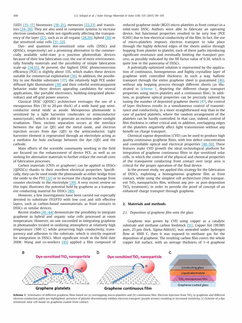
reduced graphene oxide (RGO) micro-platelets as front contact in asolid-state DSSC. Authors were able to fabricate an operatingdevice, but functional properties resulted to be very low (PCE0.26%) due to low electrical conductivity of the film. In fact, the useof micro-platelets imposes electron transport to take placethrough the highly defected edges of the sheets and/or throughhopping from platelet to platelet, each of these paths introducingsignificant resistance and eventually limiting the transport pro-cess, as possibly indicated by the fill factor value of 0.36, which isquite low in the panorama of DSSCs.
A potentially optimized solution is represented by the applica-tion of continuous, homogeneous and highly crystalline layer ofgraphene with controlled thickness. In such a way, ballistictransport through the entire graphene sheet is guaranteed [46],without any hopping process through different sheets (as illu-strated in Scheme 1, depicting the different charge transportproperties using micro-platelets and a continuous film). In addi-tion, as graphene optical properties can be precisely tailored bytuning the number of deposited graphene sheets [47], the controlof layer thickness results in a simultaneous control of transmit-tance and conductivity, in a more straightforward way than in thecase of packed platelets, where the random arrangement of theplatelets can be hardly controlled. In that case, indeed, control offilm thickness is rather critical and, in addition, overlapping edgesof the platelets negatively affect light transmission without anybenefit on charge transport.
Chemical vapour deposition (CVD) can be used to produce highquality continuous graphene films, with low defect concentrationand controllable optical and electrical properties [48–50]. Thesefeatures make CVD growth the ideal technological platform forintegration of graphene continuous films in dye sensitized solarcells, in which the control of the physical and chemical propertiesof the transparent conducting front contact over large area iscritical for the proper operation of the final device.
In the present study, we applied this strategy for the fabricationof DSSCs, exploiting a homogeneous graphene film as frontcontact, while using the simplest cell architecture (thin transpar-ent TiO2 nanoparticles film, without any pre- or post-depositionTiCl4 treatment), in order to provide the proof of concept of anenhanced charge transport through graphene.
2. Materials and methods
2.1. Deposition of graphene film onto the glass
Graphene was grown by CVD using copper as a catalyticsubstrate and methane carbon feedstock [51]. Copper foil (99.98%pure, 25 μm thick, Sigma-Aldrich), was annealed under hydrogenflow at 1000 1C, then it was exposed to methane gas for thedeposition of graphene. The resulting carbon film covers the wholecopper foil surface, with an average thickness of 1–4 graphene
Scheme 1. Schematics of different graphene films based on (a) overlapping micro-platelets and (b) continuous film. Electron injection from TiO2 to graphene and differentelectron conduction paths are highlighted: presence of platelet discontinuity inhibits electron transport (purple arrows) resulting in increased resistivity. (c) Scheme of a dyesensitized solar cell based on graphene-coated front contact.
G.S. Selopal et al. / Solar Energy Materials & Solar Cells 135 (2015) 99–105100

layers. Transfer onto glass substrates is obtained by spinning a thinPMMA layer over the copper foil, then by etching the metal in aHNO3 solution (33 wt% in deionized water), rinsing it several timesin deionized water. The floating PMMA/graphene membrane isscooped from water with the target glass substrate, and let dryovernight under the hood. PMMA is removed from the glassexposing it to acetone vapors, then the substrate is finally cleanedwith isopropanol vapors.
Scanning electron microscopy (SEM) characterization was car-ried out using a LEO1530 microscope fitted out with a Schottkyemitter, while transmission electron microscopy (TEM) measure-ments were performed using a Tecnai F20 microscope equippedwith Schottky emitter and X-ray energy dispersion spectrometerfor elemental analysis.
Electrical conductivity of the glass substrate after graphenedeposition was carried out by evaporating 4 nickel contacts in Vander Pauw geometry, spaced by 0.7 mm, on the graphene film overglass and performing four point-probe measurements.
2.2. Photoanode preparation and cell assembly
Mesoporous TiO2 photoanodes were prepared by tape casting atransparent layer of 20 nm-sized anatase TiO2 nanoparticles (18NR-T from Dyesol) on graphene functionalized glass substrates.
Layers were dried for 15 min under atmospheric conditions andthen for 6 min at 120 1C. Then, all the photoanodes were annealedat 500 1C for 30 min under ambient atmosphere. Film thicknesswas controlled through the number of TiO2 casted layers andmeasured by profilometry.
Dye sensitization was performed using a 5.0 mM solution ofN719 dye in ethanol (5 h soaking).
DSSCs cells were fabricated by sandwiching the sensitized TiO2
photoanode and a Pt-sputtered FTO glass (Pt film thickness: 5 nm)counter electrode using 25 μm thick plastic spacer. The spacebetween electrodes was filled with redox electrolyte, whosecomposition was the following: 0.1 M LiI, 0.05 M I2, 0.6 M 1,2-dimethyl-3-n-propylimidazolium iodide, and 0.5 M 4-tert-butyl-pyridine in acetonitrile.
The current–voltage measurements were carried out using anABET 2000 solar simulator under one sun simulated sunlight atAM 1.5 G (100 mW cm�2), calibrated with a Silicon reference cell.Active area of the cells was in the range 0.14–0.16 cm2.
The electrochemical impedance spectroscopy (EIS) was carriedout in dark conditions using a SOLARTRON 1260 An Impedance/Gain-Phase Analyzer, with an AC signal 20 mV in amplitude, in thefrequency range between 100 mHz and 300 kHz. External bias inthe range 0–900 mV was applied.
3. Results and discussion
Fig. 1a shows a SEM image of the graphene film transferred ona glass substrate. The graphene appears darker than the non-conductive glass. The film is composed by a rather continuousgraphene layer, with thicker small graphene islands, providingcontinuous electrical paths over several centimeters. Film thick-ness has been estimated by transferring samples grown under thesame conditions onto standard TEM grid with a perforated carbonsupport film. Fig. 1b shows the TEM micrograph of the graphenefilm spanning over the carbon substrate. In the inset of Fig. 1b ahigher magnification view of a folded edge of the film reveals thelocal thickness of the membrane, composed of two graphenelayers. The sheet resistance, performed over an area of 1 cm2,ranged from 0.5 kΩ/□ to 1.0 kΩ/□.
Digital picture of homogeneous CVD graphene layer transferredon bare glass over its whole surface is shown in Fig. 2 before andafter deposition of TiO2 mesoporous layer sensitized with commer-cial N719 dye. Transparency of graphene film can be appreciatedand quantitative comparison with FTO and ITO glass is reported inFig. 3a. Precisely square shaped TiO2 thin film was deposited ongraphene layer, without any post-deposition shaping. The relatively
Table 1Functional properties of DSSCs under simulated sunlight (1 sun, AM 1.5 G,100 mW cm�2) as a function of photoanode thickness.
Front contact TiO2 thickness (μm) Voc (mV) Jsc (mA cm�2) FF (%) PCE (%)
Graphene film 1.4 620 3.6 28 0.62.4 670 5.7 32 1.23.0 640 6.3 30 1.24.2 630 7.8 40 2.0
RGO plateletsn 2.5–3.0 700 1.0 36 0.26
n Results from Ref. [45].
Fig. 1. Characterization of the transferred graphene film. (a) SEM micrograph of the CVD grown graphene transferred on glass substrate. Graphene appears with darkercontrast compared to the insulating substrate. (b) TEM micrograph of the film transferred on perforated carbon grids for structural characterization. (Inset) High-resolutiondetail of a folded edge in a bi-layer region of the film.
G.S. Selopal et al. / Solar Energy Materials & Solar Cells 135 (2015) 99–105 101

low temperature of the annealing, together with the moderate timeof heating, is not expected to heavily damage the graphene layer.Nevertheless, it is reasonable to expect that the annealing willinduce the occurrence of lattice defects and a mild oxidation of thegraphene layer, slightly reducing the in-plane conductance. [52–54]At this stage we did not perform an extensive structural or electricalcharacterization of the graphene layer nor of the TiO2/grapheneinterface, relying on the analysis of the overall cell performance tocheck the functional integrity of the graphene electrode, whichwould require a dedicated deep investigation, beyond the main aimof the present study. Good dye uptake can be appreciated from thehomogeneous color of the TiO2 film after soaking, which testifiesthe good adhesion of TiO2 and the homogeneous thickness of thephotoanodes. Transmittance spectra of the photoanode during thevarious preparation steps are reported in Fig. 3b. Shift of the onsetof absorbance from around 310 nm (bare glass) to 380 nm after TiO2
deposition is due to direct band gap absorption from TiO2. Dyeloading is successfully carried out, and the photoanode shows thetypical absorption spectrum featuring maximum absorption around500 nm, according to N719 optical properties.
Photoanodes with controlled TiO2 layer thickness (rangingbetween 1.4 and 4.2 μm) have been prepared and integrated inDSSCs. Corresponding device functional properties are reported in
Fig. 4 and in Table 1. As expected for this range of thicknesses,DSSCs exhibit an increasing PCE as a function of TiO2 layerthickness mainly related to the increased photogenerated currentas a consequence of almost linear increase of the optical densitywith film thickness (as shown in Fig. 4d). In this respect, both opencircuit photovoltage (Voc) and fill factor (FF) play a minor role inboosting PCE.
Recorded PCE is relatively high as compared with devicesoperating with similar TiO2 photoanodes (as for titania nanopar-ticle size and film thickness): this result is attributable to theexcellent transport properties of the graphene film based frontelectrode, which is able to collect most of the photogeneratedcharges. Present results are compared with the most similarstructure reported in literature, which is an all solid-state DSSC(Fig. 4b) [45]. Even taking into account that standard solid-stateDSSCs perform poorly as compared to their liquid counterparts[55], the result obtained in the present study is quite relevant,since a PCE more than 7 times higher (2.0% as compared to 0.26%)is here recorded. By considering photoanodes of the same thick-ness of Ref. [45] (around 2.6 μm) the increase in PCE is around4.5 times (from 0.25% to 1.2%). Our result is even more remarkableby considering that in Ref. [45] a TiO2 blocking layer was applied,aimed at inhibiting electron back reaction from the graphene sheet
Fig. 2. Digital pictures of graphene coated glass before (a) and after deposition of TiO2 mesoporous layer and impregnation with N719 dye (b).
Fig. 3. Transmittance UV–vis spectra of photoanodes during the different fabrication steps. (a) graphene (black line), ITO (grey dashed line) and FTO (grey solid line) on glass.(b) Graphene on glass (black line), TiO2 on graphene (grey line), sensitized graphene–TiO2 photoanode (red line). (For interpretation of the references to color in this figurelegend, the reader is referred to the web version of this article.)
G.S. Selopal et al. / Solar Energy Materials & Solar Cells 135 (2015) 99–105102

to the electrolyte, which is responsible for charge recombinationfrom the front contact to the hole transporter, that reduces theoverall PCE. In our case, no blocking layer was applied, implyingthat potential improvements can be promptly achieved.
To give rational understanding of the functional behavior ofgraphene, we applied electrochemical impedance spectroscopy(EIS), identifying the usually accepted transmission line of operat-ing DSSC [56], whose main outcomes are reported in Fig. 5.
Fig. 4. (a) Current density–voltage curves of DSSCs for different photoanode thickness d, (see Table 1 for the thickness of the different layers) under simulated sunlight (AM1.5 G, 100 mW cm�2). (b) Current density–voltage curve of the best operating cell (blue inverted triangles) compared to the best literature result obtained using RGOplatelets (digitized data from Ref. [45] for an all solid-state DSSC). (c) PCE and (d) Jsc as a function of TiO2 thickness of the cells reported in (a). (For interpretation of thereferences to color in this figure legend, the reader is referred to the web version of this article.)
Fig. 5. (a) Nyquist diagram of DSSC cell based on graphene conducting layer on glass (selected bias only are reported). (b) The series resistance RS accounting for electrontransport at the front contact was calculated and reported in the figure, comparing the values with the resistance measured for a cell made with FTO glass.
G.S. Selopal et al. / Solar Energy Materials & Solar Cells 135 (2015) 99–105 103

Through EIS analysis, the series resistance of the graphene sheetinside the cell is determined. As well-established from the theoryof EIS applied to DSSCs, we can associate one element of theequivalent circuit applied to fit the experimental results to thesheet resistance of the TCO.
In the Nyquist plot (Fig. 5a), the displacement from zero of thehigh frequency semicircle corresponds to the series resistancerelated to the sheet resistance of the front conducting glass andthe contact series of the cell (data referring to the best device areconsidered). The value of this resistance is about (421711)Ω(calculated in the whole range of the working bias applied on thecell), which is an excellent value compared with resistancesdetected by Wang and coworkers [45]. However, direct compar-ison of sheet resistances of graphene and FTO (both reported inFig. 5b) highlights the latter is still better: this issue is of course ofrelevance and should deserve further improvements in the processof deposition of graphene onto the glass substrate, which isbeyond the scope of the present study. It is indeed worthmentioning that sheet resistance of graphene-based front electro-des has been identified as an issue in all the mentioned studiesdealing with the same topic. In this sense, the annealing inatmosphere required for the deposition of the TiO2 layer overthe graphene covered glass is increasing its sheet resistance. Thiseffect and the overall in-plane conductivity of the graphene layeris a point deserving further attention in view of optimizingeffective integration of this material in high performance solarenergy converting devices.
4. Conclusions and perspectives
We demonstrated for the first time that a continuous andhomogeneous layer of graphene grown by CVD can be applied inhigh efficiency operating DSSCs even after high temperaturesintering. The standard steps for preparation of DSSCs (i.e. TiO2
casting and sintering, dye loading and cell assembly) are compa-tible with the proposed graphene front contact. We obtained anoutstanding PCE of 2%, which is almost 8 times higher thanprevious achievements in comparable devices.
Key point for the increment of cell performances relies on theincrease of conductivity of graphene layer, possible by applying ahomogeneous large area film, on the strong adhesion to thesubstrate and on the conformal coverage of the conducting layerwith TiO2 film without any detachment. These results foreseeeffective exploitation of graphene front contact for a wide range ofapplications, in which transparent conducting layers are requiredwithout the restrictions, which typically affect the TCO materials.
Acknowledgements
R.M. acknowledges Regione Lombardia and European Commis-sion for funding under Project “Dote Ricercatori e Dote RicercaApplicata” (POR FSE 2007-13). A.V. acknowledges the EuropeanCommission for partial funding under the contract F-Light MarieCurie no 299490. The authors acknowledge the European Com-mission for partial funding under the contract WIROX no 295216.A.V. and I.C. acknowledge Regione Lombardia for partial fundingunder the contract “Tecnologie e materiali per l’utilizzo efficientedell’energia solare”. G.S.S. acknowledges OIKOS s.r.l. for funding.
References
[1] I. Hamberg, C.G. Granqvist, Evaporated Sn2 doped In2O3 films: basic opticalproperties and applications to energy efficient windows, J. Appl. Phys. 60(1986) 123–160.
[2] C.G. Granqvist, Transparent conductors as solar energy materials: a panoramicreview, Sol. Energy Mater. Sol. Cells 91 (2007) 1529–1598.
[3] C. Celle, C. Mayousse, E.O. Moreau, H. Basti, A. Carella, J.P. Simonato, Highlyflexible transparent film heaters based on random networks of silver nano-wires, Nano Res 5 (2012) 427–433.
[4] K.D.M. Rao, G.U. Kulkarni, A highly crystalline single Au wire network as a hightemperature transparent heater, Nanoscale 6 (2014) 5645–5651.
[5] A. Andersson, N. Johansson, P. Bröms, N. Yu, D. Lupo, W.R. Salaneck, Fluorinetin oxide as an alternative to indium tin oxide in polymer LEDs, Adv. Mater.10 (1998) 859–863.
[6] N. Chantarat, Y.W. Chen, S.H. Hsu, C.C. Lin, M.C. Chiang, S.Y. Chen, Effect ofoxygen on the microstructural growth and physical properties of transparentconducting fluorine-doped tin oxide thin films fabricated by the spraypyrolysis method, ECS J. Solid State Sci. Technol. 2 (2013) 131–135.
[7] Y. Sun, J.A. Rogers, Inorganic semiconductors for flexible electronics, Adv.Mater. 15 (2007) 1897–1916.
[8] S. De, T.M. Higgins, P.E. Lyons, E.M. Doherty, P.N. Nirmalraj, W.J. Blau, J.J. BolandJ.N. Coleman, Silver nanowire networks as flexible, transparent, conducting films:extremely high DC to optical conductivity ratios, ACS Nano 3 (2009) 1767–1774.
[9] Z. Wu, Z. Chen, X. Du, J.M. Logan, J. Sippel, M. Nikolou, K. Kamaras,J.R. Reynolds, D.B. Tanner, A.F. Hebard, A.G. Rinzler, Transparent conductivecarbon nanotube films, Science 305 (2004) 1273–1276.
[10] A. Du Pasquier, H.E. Unalan, A. Kanwal, S. Miller, M. Chhowalla, Conductingand transparent single-wall carbon nanotube electrodes for polymer–full-erene solar cells, Appl. Phys. Lett. 87 (2005) 203511.
[11] N. Ferrer-Anglada, J. Pérez-Puigdemont, J. Figueras, M. Zahir Iqbal, S. Roth,Flexible, transparent electrodes using carbon nanotubes, Nanoscale Res. Lett.7 (2012) 571.
[12] S. Pang, Y. Hernandez, X. Feng, K. Müllen, Graphene as transparent electrodematerial for organic electronics, Adv. Mater 23 (2011) 2779–2795.
[13] Y. Zhu, S. Merali, W. Cai, X. Li, W. Suk, J.R. Potts, R.S. Ruoff, Graphene andgraphene oxide: synthesis, properties, and applications, Adv. Mater 22 (2010)3906–3924.
[14] L.G. De Arco, Y. Zhang, C.W. Schlenker, K. Ryu, M.E. Thompson, C. Zhou,Continuous, highly flexible, and transparent graphene films by chemical vapordeposition for organic photovoltaics, ACS Nano 4 (2010) 2865–2873.
[15] Y.S. Kim, K. Joo, S. Jerng, J.H. Lee, D. Moon, J. Kim, E. Yoon, S. Chun, Directintegration of polycrystalline graphene into light emitting diodes by plasma-assisted metal-catalyst-free synthesis, ACS Nano 8 (2014) 2230–2236.
[16] N. Li, S. Oida, G.S. Tulevski, S. Han, J.B. Hannon, D.K. Sadana, T. Chen, Efficientand bright organic light-emitting diodes on single-layer graphene electrodes,Nat. Commun 4 (2013) 2294.
[17] D. Ick Son, B. Wook Kwon, D. Hee Park, W. Seo, Y. Yi, B. Angadi, C. Lee, W. KookChoi, Emissive ZnO–graphene quantum dots for white-light-emitting diodes,Nat. Nanotechnol. 7 (2012) 465–471.
[18] Q.Y. He, H.G. Sudibya, Z.Y. Yin, S.X. Wu, H. Li, F. Boey, W. Huang, P. Chen, H. Zhang,Centimeter-long and large-scale micropatterns of reduced graphene oxide films:fabrication and sensing applications, ACS Nano 4 (2010) 3201–3208.
[19] Z.J. Wang, X.Z. Zhou, J. Zhang, F.Y.C. Boey, H. Zhang, Direct electrochemicalreduction of single-layer graphene oxide and subsequent functionalizationwith glucose oxidase, J. Phys. Chem. C 113 (2009) 14071–14705.
[20] Z.J. Wang, J. Zhang, P. Chen, X.Z. Zhou, Y.L. Yang, S.X. Wu, L. Niu, Y. Han,L.H. Wang, P. Chen, F. Boey, Q.C. Zhang, B. Liedberg, H. Zhang, Label-free,electrochemical detection of methicillin-resistant staphylococcus aureus DNAwith reduced graphene oxide-modified electrodes, Biosens. Bioelectron.26 (2011) 3881–3886.
[21] X.H. Cao, Q.Y. He, W.H. Shi, B. Li, Z.Y. Zeng, Y.M. Shi, Q.Y. Yan, H. Zhang,Graphene oxide as a carbon source for controlled growth of carbon nanowires,Small 7 (2011) 1199–1202.
[22] J.Q. Liu, Z.Y. Yin, X.H. Cao, F. Zhao, A. Ling, L.H. Xie, Q.L. Fan, F. Boey, H. Zhang,W. Huang, Bulk heterojunction polymer memory devices with reducedgraphene oxide as electrodes, ACS Nano 4 (2010) 3987–3992.
[23] J.Q. Liu, Z. Lin, T. Liu, Z.Y. Yin, X.Z. Zhou, S. Chen, L.H. Xie, F. Boey, H. Zhang,W. Huang, Multilayer stacked low-temperature-reduced graphene oxidefilms: preparation, characterization, and application in polymer memorydevices, Small 6 (2010) 1536–1542.
[24] Q.Y. He, S.X. Wu, S. Gao, X.H. Cao, Z.Y. Yin, H. Li, P. Chen, H. Zhang, Transparent,flexible, all-reduced graphene oxide thin film transistors, ACS Nano 5 (2011)5038–5044.
[25] B. Li, X.H. Cao, H.G. Ong, J.W. Cheah, X.Z. Zhou, Z.Y. Yin, H. Li, J.L. Wang, F. Boey,W Huang, H. Zhang, All-carbon electronic devices fabricated by directly grownsingle-walled carbon nanotubes on reduced graphene oxide electrodes, Adv.Mater. 22 (2010) 3058–3061.
[26] H.G. Sudibya, Q.Y. He, H. Zhang, P. Chen, Electrical detection of metal ionsusing field-effect transistors based on micropatterned reduced grapheneoxide films, ACS Nano 5 (2011) 1990–1994.
[27] M. Sangermano, A. Chiolerio, G.P. Veronese, L. Ortolani, R. Rizzoli,F. Mancarella, V. Morandi, Graphene–epoxy flexible transparent capacitorobtained by graphene–polymer transfer and UV-induced bonding, Macromol.Rapid Commun. 35 (2014) 355–359.
[28] G. Eda, Y.Y. Lin, S. Miller, C.W. Chen, W.F. Su, M. Chhowalla, Transparent andconducting electrodes for organic electronics from reduced graphene oxide,Appl. Phys. Lett. 92 (2008) 233305.
[29] Z.Y. Yin, S.Y. Sun, T. Salim, S.X. Wu, X. Huang, Q.Y. He, Y.M. Lam, H. Zhang,Organic photovoltaic devices using highly flexible reduced graphene oxidefilms as transparent electrodes, ACS Nano 4 (2010) 5263–5268.
G.S. Selopal et al. / Solar Energy Materials & Solar Cells 135 (2015) 99–105104

[30] Z.Y. Yin, S.X. Wu, X.Z. Zhou, X. Huang, Q.C. Zhang, F. Boey, H. Zhang,Electrochemical deposition of ZnO nanorods on transparent reduced grapheneoxide electrodes for hybrid solar cells, Small 6 (2010) 307–312.
[31] N.L. Yang, J. Zhai, D. Wang, Y.S. Chen, L. Jiang, Two-dimensional graphenebridges enhanced photoinduced charge transport in dye-sensitized solar cells,ACS Nano 4 (2010) 887–894.
[32] K.T. Dembele, G.S. Selopal, C. Soldano, R. Nechache, J.C. Rimada, I. Concina,G. Sberveglieri, F. Rosei, A. Vomiero, Hybrid carbon nanotubes�TiO2 photo-anodes for high efficiency dye-sensitized solar cells, J. Phys. Chem. C117 (2013) 14510–14517.
[33] K.T. Dembele, R. Nechache, L. Nikolova, A. Vomiero, C. Santato, S. Licoccia,F. Rosei, Effect of multi-walled carbon nanotubes on the stability of dyesensitized solar cells, J. Power Sources 233 (2013) 93–97.
[34] B. O’Regan, M. Graetzel, A Low-Cost, High-efficiency solar cell based on dye-sensitized colloidal TiO2 films, Nature 353 (1991) 737–740.
[35] A. Luque, A. Martí, A.J. Nozik, Solar cells based on quantum dots: multipleexciton generation and intermediate bands, MRS Bull 32 (2007) 236–241.
[36] S. Mathew, A. Yella, P. Gao, R. Humphry-Baker, B.F.E. Curchod, N. Ashari-Astani, I. Tavernelli, U. Rothlisberger, Md. Khaja Nazeeruddin, M. Grätzel, Dye-sensitized solar cells with 13% efficiency achieved through the molecularengineering of porphyrin sensitizers, Nat. Chem 6 (2014) 242–247.
[37] V. Galstyan, A. Vomiero, I. Concina, A. Braga, M. Brisotto, E. Bontempi, G. Faglia,G. Sberveglieri, Vertically aligned TiO2 nanotubes on plastic substrates forflexible solar cells, Small 7 (2011) 2437–2442.
[38] F.E. Ga ́lvez, E. Kemppainen, H. Míguez, J. Halme, Effect of diffuse lightscattering designs on the efficiency of dye solar cells: an integral optical andelectrical description, J. Phys. Chem. C 116 (2012) 11426–11433.
[39] J.G. Radich, R.D.P.V. Kamat, Cu2S reduced graphene oxide composite for high-efficiency quantum dot solar cells. overcoming the redox limitations of S2�/Sn2� at the counter electrode, J. Phys. Chem. Lett. 2 (2011) 2453–2460.
[40] J.D. Roy-Mayhew, I.A. Aksay, Graphene materials and their use in dye-sensitized solar cells, Chem. Rev. 12 (2014) 6323–6348.
[41] H. Park, S. Chang, J. Jean, J.J. Cheng, P.T. Araujo, M. Wang, M.G. BawendiM.S. Dresselhaus, V. Bulović, J. Kong, S. Gradečak, Graphene cathode-basedZnO nanowire hybrid solar cells, Nano Lett. 13 (2013) 233–239.
[42] X. Wang, L. Zhi, N. Tsao, Ž. Tomović, J. Li, K Müllen, Transparent carbon films aselectrodes in organic solar cells, Angew. Chem. Int. Ed. 47 (2008) 2990–2992.
[43] J. Wu, H.A. Becerril, Z. Bao, Z. Liu, Y. Chen, P. Peumans, Organic solar cells withsolution-processed graphene transparent electrodes, Appl. Phys. Lett.92 (2008) 263302.
[44] H. Bi, F. Huang, J. Liang, X. Xie, M. Jiang, Transparent conductive graphenefilms synthesized by ambient pressure chemical vapor deposition used as thefront electrode of CdTe solar cells, Adv. Mater. 23 (2011) 3202–3206.
[45] X. Wang, L. Zhi, K. Müllen, Transparent, conductive graphene electrodes fordye-sensitized solar cells, Nano Lett. 8 (2008) 323–327.
[46] P. Avouris, Graphene: electronic and photonic properties and devices, NanoLett. 10 (2010) 4285–4294.
[47] F. Bonaccorso, Z. Sun, T. Hasan, A.C. Ferrari, Graphene photonics and optoelec-tronics, Nat. Photon 4 (2010) 611–622.
[48] S. Santangelo, G. Messina, A. Malara, N. Lisi, T. Dikonimos, A. Capasso,L. Ortolani, V. Morandi, G. Faggio, Taguchi optimized synthesis of graphenefilms by copper catalyzed ethanol decomposition, Diamond Relat. Mater.41 (2014) 73–78.
[49] G. Faggio, A. Capasso, G. Messina, S. Santangelo, T. Dikonimos, S. Gagliardi,R. Giorgi, V. Morandi, L. Ortolani, N. Lisi, High-temperature growth ofgraphene films on copper foils by ethanol chemical vapor deposition, J. Phys.Chem. C 117 (2013) 21569–21576.
[50] X. Li, W. Cai, J. An, S. Kim, J. Nah, D. Yang, Large-area synthesis of high-qualityand uniform graphene films on copper foils, Science 324 (2009) 1312–1314.
[51] X. Li, Y. Zhu, W. Cai, M. Borysiak, B. Han, D. Chen, R.D. Piner, L. Colombo,R.S. Ruoff, Transfer of large-area graphene films for high-performance trans-parent conductive electrodes, Nano Lett. 9 (2009) 4359–4363.
[52] S.P. Surwade, Z. Li, H. Liu, Thermal oxidation and unwrinkling of chemicalvapor deposition-grown graphene, J. Phys. Chem. C 38 (2012) 20600–20606.
[53] X. Wang, H. Dai, Etching and narrowing of graphene from the edges, Nat.Chem. 2 (2010) 661–665.
[54] L. Liu, S. Ryu, M.R. Tomasik, E. Stolyarova, N. Jung, M.S. Hybertsen,M.L. Steigerwald, L.E. Brus, G.W. Flynn, Graphene oxidation: thickness-dependent etching and strong chemical doping, Nano Lett. 8 (2008)1965–1970.
[55] M. Liu, M.B. Johnston, H.J. Snaith, Efficient planar heterojunction perovskitesolar cells by vapour deposition, Nature 501 (2013) 395–398.
[56] Q. Wang, S. Ito, M. Grätzel, F. Fabregat-Santiago, I. Mora-Serò, J. Bisquert,T. Bessho, H. Imai, Characteristics of high efficiency dye-sensitized solar cells,J. Phys. Chem. B 110 (2006) 25210–25221.
G.S. Selopal et al. / Solar Energy Materials & Solar Cells 135 (2015) 99–105 105