x-ray detection using the quantum-well exciton nonlinearity
TRANSCRIPT
IEEE JOURNAL OF QUANTUM ELECTRONICS. VOL 26. NO. I . JANUARY 1990 15
X-Ray Detection Using the Quantum Well Exciton Nonlinearity
Abstract-Two related schemes for detecting X-ra)\ based on 1) the wattering and 2) the reflection of a pulsed optical probe beam by car- riers produced by the absorption of a single energetic X-ray photon are described. The detection method is based on the strong carrier den- sity dependence of the (complex) index of refraction of the exciton ab- sorption lines in a GaAs/AlGaAs multiple-quantum-well structure. These schemes may be used to construct a new class of very sensitive gated X-ray detectors with micron spatial resolution and temporal res- olution in the 10-30 ps regime.
I. INTRODUCTION HE recent development of short wavelength lasers in T the X-ray regime and the interest in high density plas-
mas has brought a need for fast time-resolved and time- gated detectors which are both efficient and have good spatial resolution. Applications of these detectors include inertial confinement fusion studies, research in atomic physics of high density plasmas, in X-ray laser experi- ments, and as imaging instruments for microscopic and holographic applications. The detectors described in this paper would be sensitive only to the highest energy lab- oratory X-ray lasers currently under development.
Currently, gated X-ray detectors are based on micro- channel plate technology. The spatial resolution is limited by fiber diameter to tens of microns, and the temporal resolution is in the vicinity of 200 ps [ 11, [ 2 ] . Microchan- ne1 plate detectors have efficiencies of around 5-15 per- cent in the soft X-ray regime depending upon the wave- length of the incident photons and the angle of incidence
This paper proposes two new detection schemes based on the use of optical nonlinearities of multiple quantum well (MQW) structures to obtain potentially fast (10 ps) and efficient X-ray detectors with very high ( < 1 pm) spatial resolution.
In optical switching experiments using MQW struc- tures, an optical beam above the bandgap produces car- riers which in turn modify the absorption coefficient and index of refraction in the vicinity of exciton absorption lines. A second optical (probe) beam which is tuned at or
[31, ~41.
Manuscript received March 21, 1988: revised August IO. 1989. Thls work was supported in part by a grant from the Arthur D. Little Company. by the M. I . T . Vinton-Hayes Fund (P . L . H . ) , and by the TRW Fellow- ship Program (C. C. E.).
The authors are with the Research Laboratory of Electronics. Massa- chusetts Institute of Technology. Cambridge. M A 02 139.
IEEE Log Number 8931617.
near the exciton absorption line can be modulated or switched by the first beam.
The enhancement of these nonlinearities has been im- proved substantially during the past decade, especially in MQW materials such as GaAs/AlGaAs [ 5 ] , [ 6 ] . Optical nonlinearities can easily be seen at room temperatures with relatively small carrier generation [7], [ 81.
We propose to produce carriers through direct absorp- tion of X-rays in an MQW structure (in essence replacing the first optical beam), which can in principle lead to modulation of the optical probe beam. The basic effect is relatively weak due to the small number of carriers pro- duced following the absorption of a single X-ray photon.
Two schemes are proposed to take advantage of the ef- fect in order to allow detection of single X-ray photons. In the first scheme a homogeneous MQW structure is used, and the detection scheme is based on wide-angle scattering of the optical probe from a local disturbance in the (complex) index of refraction produced by carriers re- sulting from the absorption of a single X-ray photon. The second approach uses microetalons with high cavity fi- nesse to enhance the effects of small changes in refractive index. In this scheme the microetalons are arranged such that the reflectivity is increased by a detectable amount following the absorption of an X-ray photon.
This paper is arranged as follows. In Section 11, we dis- cuss aspects of the X-ray-optical nonlinearity and the MQW detector structure. The planar approach to X-ray detection is described in Section 111. In Section IV we introduce the microetalon version of the detector. In Sec- tion V we model the noise and the avalanche effect as well as estimate the signal for both the planar and the microe- talon schemes, and in Section VI we summarize our re- sults.
11. X-RAY ABSORPTION A N D RESULTING INDEX MODULATION
The detector schemes are based on the observation of small changes of refractive index in a GaAs/AlGaAs MQW structure due to the presence of carriers generated by photoabsorption of X-rays. This can be accomplished by propagating an optical probe beam through the mate- rial and observing (imaging) either wide angle scattered light (planar detector approach) or modifications in the reflected light (microetalon approach). Below we describe how we believe the carrier generation process occurs.
0018-9197/90/0100-0075$01 .OO O 1990 IEEE
-
76 IEEE J O U R N A L OF Q U A N T U M ELECTRONICS. VOL. 26, NO. I . JANUARY 1990
An ipcident (500 eV ) X-ray penetrates approximately 2000 A [9] into the front surface of a multiple quantum well AlGaAs /GaAs structure where it generates high-en- ergy carriers through inner-shell photoionization and Au- ger ionization (see Fig. 1) . A small-scale collisional av- alanche follows since essentially all of the initial, very hot carriers have sufficient energy to ionize outer shell elec- trons of the neutral lattice atoms. This process happens very rapidly (on the order of a picosecond). The carriers also interact with the lattice, losing energy to optical pho- nons.
The above secondary emission process results in an average residual kinetic energy of individual carriers that is roughly that of the band-gap energy (at this point no further pair production occurs). The carriers lose this re- sidual energy through thermalization with the lattice with an associated time constant of approximately 10 ps [ 101. The effective bandgap Eeff for carrier production (includ- ing the above effects) can be written as [ 111
where E, is the actual bandgap, E is the average energy loss to optical phonons per ionization event, and E, is the residual kinetic energy of the carriers after they can no longer produce ionization. The number of electron-hole pairs generated is given by
Ph
where hu is the photon energy of the incident X-ray. The carriers diffuse radially and isotropically during the
thermalization process. Initially, the carriers are energetic enough (average energies on the order of the band-gap energy, approximately 1.46 eV) so that the presence of the quantum wells (which are about 0 .3 eV deep) have little effect on the motion of the carriers. The carrier dis- tribution is nearly spherically symmetric with a Gaussian radial dependence during the thermalization process. This is depicted schematically in Fig. 1. The volume of the sphere increases with time, until the boundaries of the quantum wells begin to slow the diffusion in the z direc- tion (normal to the quantum wells). This corresponds to roughly a time of 5 ps after the X-ray was absorbed and to a sphere with a radius of 0.1 pm. Diffusion after this time occurs primarily in the x and y directions (parallel to the quantum wells) and the initial spherical region con- taining the carriers begins to resemble an ellipse.
As an example if E,,, is equal to 4.35 eV for GaAs [ 121, then in principle as many as 115 electron-hole pairs could be generated following the absorption of a 500 eV photon. The number of carriers created can be increased by using smaller band-gap materials such as InAs or InSb, but for this paper we choose to do the theoretical calculations with GaAs since optical data is more readily available for this material.
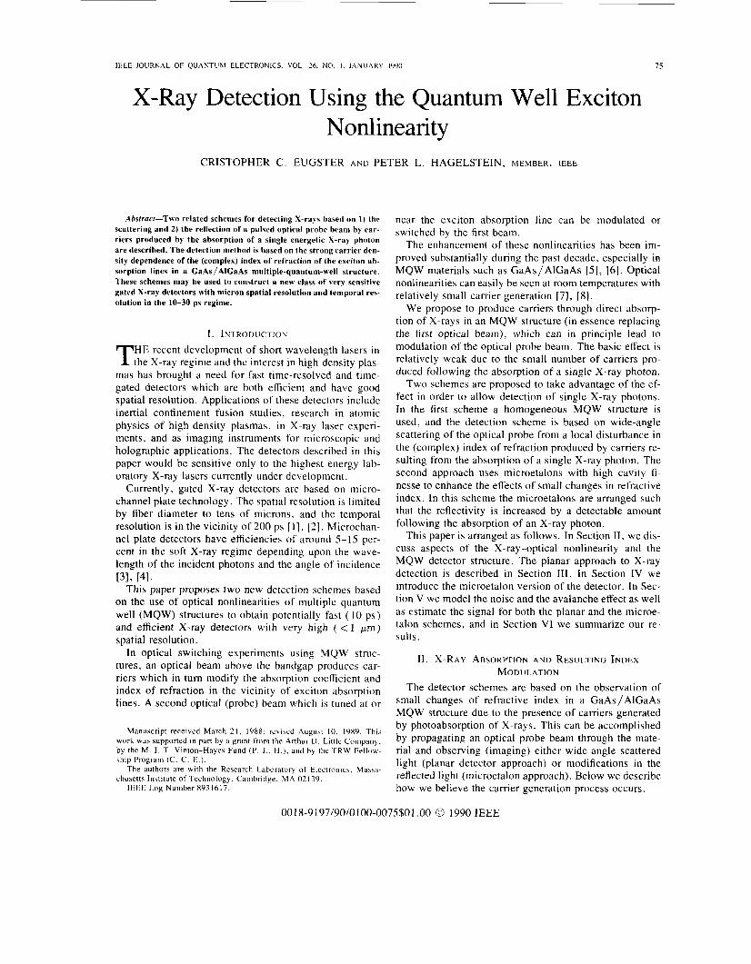
Multiple Quantum Wells (MQW) I Substrate (Sb)
Fig. 1 . Schematic illustrating the X-ray generated carriers in the multiple quantum well structure. The dimensions of the quantum well structure are roughly 3 x 3 mm with a depth in the range of microns.
The X-ray carrier conversion process can potentially be enhanced through the placement of deep donor and accep- tor impurities in the region where carrier generation oc- curs. The idea is that the residual kinetic energy could be used to ionize impurity atoms whose ionization energies correspond to the donor and acceptor levels which are less than the band-gap energies. For a more detailed discus- sion of using impurities in the converter region see the Appendix.
Once a sufficiently high concentration of carriers are in the quantum wells, their effects on the index of refraction become important. The effect of carrier density on optical constant is strongest in the vicinity of the exciton absorp- tion lines just below the bandgap (near 1.45 eV for the data of [13], on which the numbers in this paper are based). At this point it is appropriate to generalize the coefficients (T,h (the change in the absorption coefficient produced by one electron-hole pair per unit volume) and neh (the change in the refractive index produced by one electron-hole pair per unit volume), as
where Neh is the change in the complex refractive index produced by one electron-hole pair per unit volume, and k,, is the free space propagation constant.
The exciton line shapes are sensitive to carrier density (as a result of phase-space filling and exchange [ 141 ), and the change in the complex refractive index is described by
An = pNch
where p is the excess density of electron-hole pairs in the quantum wells due to the absorption of the incident pho- ton (we assume that the background carrier density is small and not localized). The change in index An creates enough of a perturbation in the optical probe beam such that modulation of the scattered (in the planar detection scheme) or reflected (in the microetalon detection scheme) optical radiation can be detected.
The number of electron-hole pairs N,. produced by a single X-ray photon is sufficient to cause line shape mod- ification if a sufficient carrier density is trapped by the quantum wells. If we assume that the radius of the sphere containing the electrons and holes at the time when they are trapped by the quantum wells to be 0.1 pm, then an average density of 3.4 x 10l6 pairs/cm3 within the wells exists for the 115 elecpon-hole pairs from our example above, assuming 100 A well size and 20 A barriers. The
(4)
EUGSTER A N D HAGELSTEIN. X-RAY DETECTION USING QW EXCITON NONLINEARITY I1
largest magnitude of n e h occurs near the peak of the lowest exciton absorption line, and is approximately 3.7 X IO-'' cmP3 [13]. As a result, a modulation of the real part of the index of refraction of 1.3 X lop2 is expected.
The imaginary part of the index of refraction corre- sponds to absorption, and the maximum change in ab- sorption is estimated to be (-7.0 X cm2) X ( 3 . 4 x lOI6/cm3) = -2400 cm-' in the vicinity of the ab- sorbed X-ray photon (as compared to a total absorption of 1.2 x IO4 cm- I for the nonirradiated surface). The point of these estimates is that a relatively small number of lo- calized carriers can provide a sufficiently large density to cause interestingly large line shape modification.
If the optical probe beam is tuned to just below the long wavelength part of the lower (heavy hole) absorption line, then the modification in optical constant due to carrier concentration is weaker. Nevertheless, this regime offers the possibility of providing an enhancement in the number of carriers present through an avalanche mechanism. For example, the exciton absorption lines arise from the pro- cess by which an electron-hole pair is created into an ex- citonic state. If the absorption coefficient is greater in the presence of X-ray produced carriers, then the optical probe causes a larger production rate of excitons (and hence car- riers, since the excitons ionize in a fraction of a pico- second at room temperature), which in turn leads to a still larger production rate of excitons due to the presence of the new carriers, and so forth until saturation occurs.
For example, in the vicinity of 1.451 eV, the primary exciton absorption coefficient is somewhat less than 950 cm-' [ 131. The incremental absorption coefficient due to the presence of 3.4 X 1OI6 pairs/cm3 is close to 900 cm-' (leading to a total absorption coefficient of 1850 cm-' in the X-ray absorption region). As a result, it seems pos- sible to significantly increase the number of carriers in the region of X-ray absorption relative to surrounding re- gions. However, the carriers generated in nonirradiated sectors would in general lead to noise in the system as discussed in Section V.
The probe beam can also be tuned to very long wave- lengths ( < 1.44 eV) such that not many carriers are cre- ated. In this region there is no avalanche effect, allowing the energy per unit area of the probe beam to be increased without saturating the device since very little absorption takes place. By increasing the energy per unit area of the probe beam, more signal photons can be obtained without the noise associated with the avalanche effect.
Due to the saturation of the nonlinearity, larger total effects are obtained through populating a greater number of quantum wells rather than having higher carrier con- centrations in a fixed number of wells. There exists the possibility to populate more quantum wells outside the region of initial expansion (in this case the quantum wells would have to be "lossy" to allow tunneling of carriers to neighboring quantum wells). In this manner the region could increase in the z direction (direction of probe beam propagation), resulting in a larger reflected or scattered optical signal.
111. X-RAY DETECTION USING PLANAR STRUCTURES
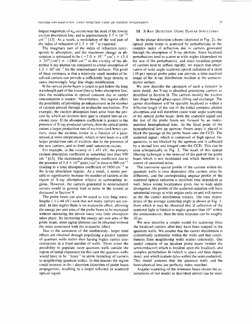
In the planar detection scheme (depicted in Fig. 2) , the optical probe beam is scattered by perturbations in the complex index of refraction due to carriers generated through the absorption of X-ray photons. Since localized perturbations tend to scatter at wide angles (dependent on the size of the perturbation), and since localized groups of carriers tend to diffuse rapidly, we expect that obser- vation of wide angle scattered optical radiation of a short (10 ps) optical probe pulse can provide a time-resolved image of the X-ray distribution incident at the semicon- ductor surface.
We now describe the operation of such a detector in more detail. An X-ray is absorbed generating carriers as described in Section 11. The carriers modify the exciton line shape through phase-space filling and exchange. The carrier distribution will be spatially localized to within a diffusion length of the site of the initial energetic photon absorption and will therefore cause wide angle scattering of the optical probe beam. Both the scattered signal and the rest of the probe beam are focused by an index- matched hemispherical lens. At the focal point of the hemispherical lens an aperture (beam stop) is placed to block the passage of the probe beam onto the CCD. The scattered signal, which is composed of high spatial fre- quencies, is not blocked by the aperture and is collected by a second lens and imaged onto the CCD. This can be seen schematically in Fig. 3. The result of this spatial filtering technique is the removal of the part of the probe beam which is not modulated and which therefore is a source of unwanted noise.
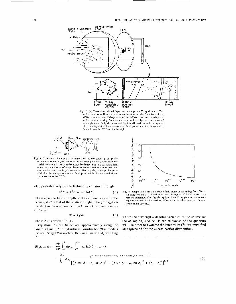
The transverse spatial profile of the carriers within the quantum wells is time dependent (the carriers relax by diffusion), and the corresponding angular profile of the scattered optical radiation is therefore time dependent as well. Since strong localization gives rise to wide angle divergence, the profile of the scattered radiation will have substantial energy at wide angles early on and will narrow as the the carrier distribution relaxes. The time depen- dence of the average scattering angle is shown in Fig. 4. from which it may be observed that if collection of the scattered light is limited to angles greater than 10" within the semiconductor, then the time response can be roughly
We now describe a simple model for scattering from the localized carriers after they have been trapped in the quantum wells. We assume that the carrier distribution is cylindrically symmetric within the wells and that contri- butions from neighboring wells scatter coherently. Our model consists of an incident probe beam (within the semiconductor) which is incident upon the localized, and complex perturbation 6k (which is space and time depen- dent), and which scatters (also within the semiconductor). This model assumes that the quantum wells and the hemispherical lens are perfectly index matched.
Angular scattering of the reference beam (under the as- sumptions of our model as described above) can be mod-
10 ps.
78 I E E E J O U R N A L OF Q U A N T U M ELECTRONICS. VOL. 26. NO. I , JANUARY 1990
Hemispherical Multiple Quantum Lens
Probe X-Ray Multiple Beam Generated Quantum
carrier Wells Fig. 2 . (a) Three-dimensional depiction of the planar X-ray detector. The
probe beam as well as the X-rays are incident o n the front face of the MQW structure. (b) Enlargement of the MQW structure showing the probe beam scattering from the carriers produced by the absorption of X-ray photons. Only the scattered light is allowed through the spatial filter (hemispherical lens. aperture at focal point. and final lens) and is focused onto the CCD on the far right.
Fig. 3. Schematic of the planar scheme showing the gated optical probe beam entering the MQW structure and scattering at wide angles from the spatial variations in the complex refractive index. Both the scattered light as well as the majority of the probe beam are focused by a hemispherical lens attached onto the MQW structure. The majority of the probe beam is blocked by an aperture at the focal plane while the scattered signal continues on to the CCD.
eled perturbatively by the Helmholtz equation through
V2E f k2E = -2k6kEl ( 5 )
where Ei is the field strength of the incident optical probe beam and E is that of the scattered light. The propagation constant in the semiconductor is k , and 6k is given in terms of An as
6k = k,An (6 )
where An is defined in (4). Equation (5) can be solved approximately using the
Green's function in cylindrical coordinates (this models the scattering from each of the quantum wells), resulting in
x-day Image
d c U
Time i n Seconds
Fig. 4. Graph depicting the characteristic angle of scattering from Gauss- ian perturbations as a function of time. Strong initial localization of the carriers generated after the absorption of an X-ray photon causes wide angle scattering. As the carriers diffuse with time the characteristic scat- tering angle decreases.
where the subscript s denotes variables at the source (at the 6k region) and A.zS is the thickness of the quantum well. In order to evaluate the integral in (7), we must find an expression for the excess carrier distribution.
EUGSTER A N D HAGELSTEIN. X-RAY DETECTION USING QW EXCITON NONLINEARITY 79
Transverse carrier diffusion within the quantum wells can be modeled by
aP P a$ 1 aP at ap; P \ aP, - + - = D y + D , , - -
where T is the recombination time and D, is the ambipolar diffusion coefficient [ 151.
Since we assume that there is no diffusion in the z di- rection after thermalization the solution to (8) which we will use to approximate the radial expansion of the spher- ically symmetric initial distribution is
( 9 )
The first exponential on the right-hand side of (9) is due to the recombination of electrons and holes while the sec- ond exponential is a result of transverse diffusion.
The scattering integral of (7) can now be evaluated to give
(10) The intensity of the scattered light is proportional to the square of the magnitude of the electric field. An expres- sion for the amount of scattered light as a function of the incident optical beam is
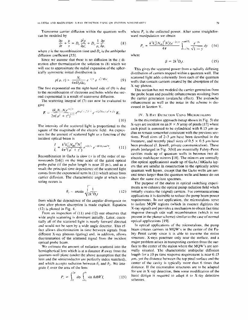
Recombination in GaAs is slow ( T is of the order of na- noseconds [ 161 ) on the time scale of the gated optical probe pulse (if the pulse length is near 10 ps), and as a result the principal time dependence of the scattered light comes from the exponential term in ( 1 1) which arises from carrier diffusion. The characteristic angle at which scat- tering occurs is
from which the dependence of the angular divergence on time after photon absorption is made explicit. Equation (12) is plotted in Fig. 4.
From an inspection of ( 1 1) and (12) one observes that wide angle scattering is dominant initially. Later, essen- tially all of the scattered light is nearly forward directed and would not be seen by a wide angle detector. This ef- fect allows discrimination in time between signals from different X-ray photons (gating) and, in addition, allows discrimination of the scattered signal from the incident optical probe beam.
We estimate the amount of radiation scattered into the hemispherical lens which is at a distance R away from the quantum-well plane (under the above assumption that the lens and the semiconductor are perfectly index matched), and which accepts radiation between 8, and 0 2 . We inte- grate I , over the area of the lens
82
01 P, = [:T d$ sin BdOR'I, (13 )
where P,. is the collected power. After some straightfor- ward manipulation we obtain
where
6 = 2k2D,t. (15)
This gives the scattered power from a radially diffusing distribution of carriers trapped within a quantum well. The scattered light adds coherently from each of the quantum wells that contain carriers created by the absorption of the X-ray photon.
This section has not modeled the carrier generation from the probe beam and possible enhancements resulting from the carrier generation (avalanche effect). The avalanche enhancement as well as the noise in the scheme is dis- cussed in Section V .
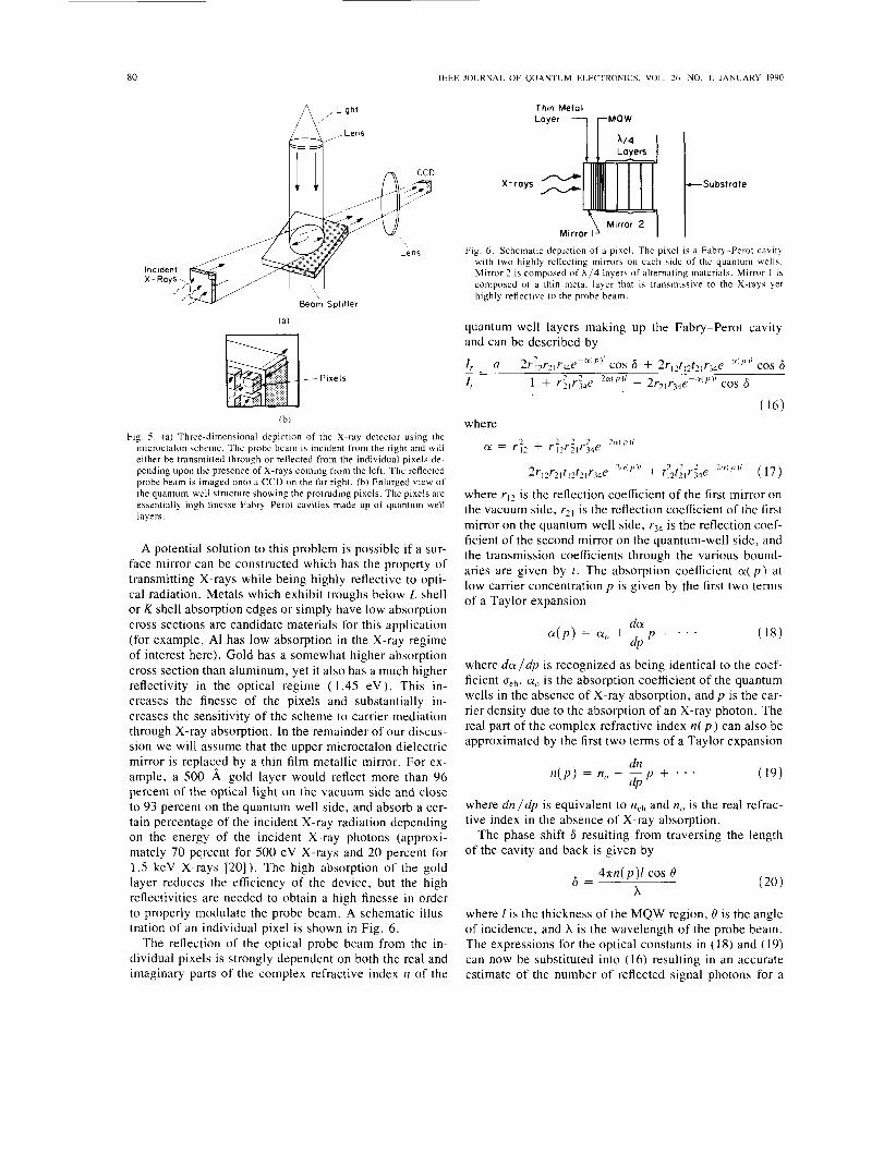
IV. X-RAY DETECTION USING MICROETALONS In the microetalon approach (setup shown in Fig. 5 ) the
X-rays are incident on an N X N array of pixels [ 171 where each pixel is assumed to be cylindrical with 0.15 pm ra- dius to remain somewhat consistent with the previous sec- tions. Pixel sizes of 2-3 pm have been described in the literature, and recently pixel sizes of 0.5 X 0.5 pm have been produced (J. Jewell, private communication). These pixels [enlarged in Fig. 5(b)] are essentially Fabry-Perot cavities made up of quantum wells in between two di- electric multilayer mirrors [ 181. The mirrors are normally (for optical applications) made up of GaAs/AlGaAs lay- ers that are similar in construction to the optically active quantum well layers, except that the GaAs wells are sev- eral times larger than the quantum wells and hence do not share the same exciton spectrum.
The purpose of the etalon in optical switching experi- ments is to enhance the optical pump radiation field which initially creates the (signal) carriers. For communications applications it is desirable to reduce the pump beam power requirements. In our application, the microetalons serve to isolate MQW regions (which in essence digitizes the X-ray signal) and provides a mechanism to obtain fast time response through side wall recombination (which is not present in the planar scheme) similar to the case of normal optical applications [ 191.
In optical applications of the microetalons, the pump beam creates carriers in MQW's in the center of the Fa- bry-Perot cavity since it is able to traverse the entire structure. X-rays penetrate only near the surface, and a major problem arises in transporting carriers from the sur- face to the center of the etalon where the MQW's are nor- mally situated. The characteristic ambipolar diffusion length for a 10 ps time response requirement is near 0.15 pm, yet the distance between the top pixel surface and the center of the cavity is typically more than 6 times that distance. If the microetalon structures are to be adapted for use in X-ray detection, then some modification of the basic design is required to adapt it to X-ray detection schemes.
80 IEEE J O U R N A L OF QUANTUM ELECTRONICS. VOL 26. NO. I . JANUARY 1990
,Light
I Lens
i l l IT
Pixels
(b)
Fig. 5. (a) Three-dimensional depiction of the X-ray detector using the microetalon scheme. The probe beam is incident from the right and will either be transmitted through or reflected from the individual pixels de- pending upon the presence of X-rays coming from the left. The reflected probe beam is imaged onto a CCD on the far right. (b) Enlarged view of the quantum well structure showing the protruding pixels. The pixels are essentially high-finesse Fabry-Perot cavities made up of quantum well layers.
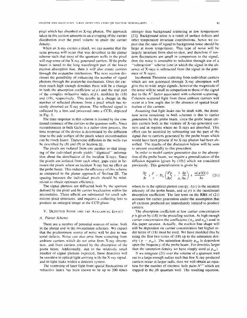
A potential solution to this problem is possible if a sur- face mirror can be constructed which has the property of transmitting X-rays while being highly reflective to opti- cal radiation. Metals which exhibit troughs below L shell or K shell absorption edges or simply have low absorption cross sections are candidate materials for this application (for example, A1 has low absorption in the X-ray regime of interest here). Gold has a somewhat higher absorption cross section than aluminum, yet it also has a much higher reflectivity in the optical regime ( 1.45 eV) . This in- creases the finesse of the pixels and substantially in- creases the sensitivity of the scheme to carrier mediation through X-ray absorption. In the remainder of our discus- sion we will assume that the upper microetalon dielectric mirror is replacFd by a thin film metallic mirror. For ex- ample, a 500 A gold layer would reflect more than 96 percent of the optical light on the vacuum side and close to 93 percent on the quantum well side, and absorb a cer- tain percentage of the incident X-ray radiation depending on the energy of the incident X-ray photons (approxi- mately 70 percent for 500 eV X-rays and 20 percent for 1.5 keV X-rays 1201). The high absorption of the gold layer reduces the efficiency of the device, but the high reflectivities are needed to obtain a high finesse in order to properly modulate the probe beam. A schematic illus- tration of an individual pixel is shown in Fig. 6.
The reflection of the optical probe beam from the in- dividual pixels is strongly dependent on both the real and imaginary parts of the complex refractive index n of the
Thin Metal
X - rays -Substrate
Fig. 6. Schematic depiction of a pixel. The pixel is a Fabry-Perot cavity with two highly reflecting mirrors on each side of the quantum wells. Mirror 2 is composed of h/4 layers of alternating materials. Mirror 1 is composed of a thin metal layer that is transmissive to the X-rays yet highly reflective to the probe beam.
quantum well layers making up the Fabry-Perot cavity and can be described by
cos 6 --N( / ' ) I cos 6 + 2r12t12t21r34e a - pLr e - a ( P ) ' 4 - I' 31 34
4 - -
1 + r;Ir:4ep2u(P)' - 2rzlr34epm'/'" cos 6
(16) where
a = rYz + r:2rilrf4e-Za(P)'
- 2r1 ?r2 t I ?tZ I r34e (17) -Zn(/J)/ + t? t' r 2 ep2"'p)/
12 21 34
where r I 2 is the reflection coefficient of the first mirror on the vacuum side, r21 is the reflection coefficient of the first mirror on the quantum well side, r34 is the reflection coef- ficient of the second mirror on the quantum-well side, and the transmission coefficients through the various bound- aries are given by r . The absorption coefficient a ( p ) at low carrier concentration p is given by the first two terms of a Taylor expansion
d a .(p) = a, + - p + . . .
dP where d a / d p is recognized as being identical to the coef- ficient a&. a(> is the absorption coefficient of the quantum wells in the absence of X-ray absorption, and p is the car- rier density due to the absorption of an X-ray photon. The real part of the complex refractive index n( p ) can also be approximated by the first two terms of a Taylor expansion
dn n ( p ) = n , + - p + * * -
dP
where d n / d p is equivalent to n e h and n,, is the real refrac- tive index in the absence of X-ray absorption.
The phase shift 6 resulting from traversing the length of the cavity and back is given by
(20) 4an( p ) I cos 8
h 6 =
where I is the thickness of the MQW region, 8 is the angle of incidence, and X is the wavelength of the probe beam. The expressions for the optical constants in (18) and (19) can now be substituted into (16) resulting in an accurate estimate of the number of reflected signal photons for a
EUGSTER A N D HAGELSTEIN: X-RAY D E T E C T I O N USING QW E X C I T O N NONLINEARITY . 81
pixel which has absorbed an X-ray photon. The approach taken in this section amounts to an averaging of the carrier distribution over the pixel volume to attain the carrier density.
When an X-ray excites a pixel, we can assume that the same process will occur that was described in the planar scheme such that most of the quantum wells in the pixel will trap some of the X-ray generated carriers. If the probe beam is tuned to the long wavelength part of the lower exciton absorption line, then i t will also create carriers through the avalanche mechanism. The next section dis- cusses the possibility of enhancing the number of signal photons through the avalanche mechanism. Once the car- riers reach high enough densities there will be a change in both the absorption coefficient a ( p ) and the real part of the complex refractive index n( p ) . modeled by ( 1 8) and (19), respectively. This results in a change in the number of reflected photons from a pixel which has re- cently absorbed an X-ray photon. The reflected signal is collected by a lens and processed onto a CCD, depicted in Fig. 5.
The time response in this scheme is limited by the con- tinued existence of the carriers in the quantum wells. Since recombination in bulk GaAs is a rather slow process, the time response of the device is determined by the diffusion time to the side surface of the pixels where recombination can be much faster. Transverse diffusion in the wells can be described by (8) and (9) in Section 111.
The pixels are isolated from one another so that imag- ing of the individual pixels yields “digitized” informa- tion about the distribution of the incident X-rays. Since the pixels are isolated from each other, gaps exist in be- tween the pixels where an incident X-ray has no effect on the probe beam. This reduces the efficiency of this scheme as compared to the planar approach of Section 111. The spacing between the individual pixels should be mini- mized to obtain optimum efficiency.
The signal photons are diffracted both by the aperture defined by the pixel and by carrier localization within the microetalon. These effects are substantial for small sub- micron pixel structures, and requires a collecting lens to produce an enlarged image at the CCD plane.
V. DETECTOR NOISE A N D T H E AVALANCHE EFFECT
A . Pluriur Scheme
There are a number of potential sources of noise, both in the planar and in the microetalon schemes. We expect that the predominant source of noise will be due to ma- terial defects. Noise can also arise from scattering from ambient carriers which do not arise from X-ray absorp- tion, and from carriers created by the absorption of the probe beam. Additionally, due to the relatively small number of signal photons expected, these detectors will be sensitive to optical light arriving with the X-ray signal, and to light leaks within a detector system.
The scattering of laser light from spatial fluctuations of refractive index has been shown to be up to 200 times
stronger than background scattering at low temperature [21]. Background noise is a result of surface defects and other temperature invariant contributions, hence we ex- pect that the ratio of signal to background noise should be large at room temperature. This type of noise will be largely invariant from shot-to-shot, and therefore if ran- dom fluctuations are small in comparison to the signal, then the noise is amenable to reduction through use of a “subtraction” scheme (one in which the signal in the ab- sence of X-rays is subtracted from the signal in the pres- ence of X-rays).
Incoherent Thomson scattering from individual carriers which are not generated through X-ray absorption will give rise to wide angle signals, however the magnitude of the noise will be small in comparison to those of the signal due to the N’ factor associated with coherent scattering. Coherent scattered light from these ambient carriers will occur at a low angle due to the absence of spatial local- ization of the carriers.
Assuming that light leaks can be dealt with, the domi- nant noise remaining in both schemes is due to carrier generation by the probe beam, since the probe beam cre- ates carriers both in the vicinity of X-ray-generated car- riers and in regions where no X-rays are absorbed. This effect can be modeled by subtracting out the part of the signal due to carriers generated by the probe beam which would have been present if no X-ray photon had been ab- sorbed. The results of the discussion below will be seen to amount essentially to this procedure.
In order to model carrier generation due to the absorp- tion of the probe beam, we require a generalization of the diffusion equation [given by ( lo) ] which we considered previously. This generalization is given by
where hu is the optical photon energy, I , ( r ) is the incident intensity of the probe beam, and a( p ) is the (nonlinear) absorption coefficient. The last term on the RHS of (21) accounts for carrier generation under the assumption that all excitons produced are immediately ionized to produce carriers.
The absorption coefficient at low carrier concentration p is given by (1 8) in the preceding section. At high enough carrier concentration the coefficients ( oeh and neb) used in this paper saturate. Actually, the exciton line shape will still be dependent on carrier concentration but higher or- der terms of (1 8) must be used. We have modeled this by using the first two terms of (1 8) up to the saturation den- sity ( p = p,,,). The saturation density pIdt is dependent upon the frequency of the probe beam. For densities larger than the saturation density we have simply used a( peat).
If we integrate (21) over the volume of a quantum well out to a large enough radius such that few X-ray-produced carriers occur at larger radii, then we will obtain an equa- tion for the number of electron-hole pairs N ” ) which are trapped in the j t h quantum well. The resulting equation,
82 IEEE JOURNAL OF QUANTUM ELECTRONICS, VOL. 26. NO. I , JANUARY 1990
augmented by additional terms accounting for tunneling between neighboring quantum wells, is given by
v 4 P )If( t > a “ J ) “ 1 ) “ 1 ) - + - + - =
at 7 2Ttun hu
where V is the volume occupied by the X-ray-produced carriers within a quantum well and where rtun is the tun- neling time between adjacent wells. The radial integration over the diffusion terms yields zero because diffusion is conservative-the total number of carriers within a well does not change as the carriers diffuse radially.
The basic picture which we have in mind is as follows. Following the initial X-ray absorption and conversion, the carriers expand through diffusion and thermalize within the quantum well layers. After thermalization the carriers can no longer diffuse between neighboring quantum wells, and purely radial diffusion augmented by axial tunneling occurs. We assume that the presence of the probe beam does not fundamentally alter our previous estimates of ra- dial diffusion. We therefore focus on the total number of electron-hole pairs in (22), and adopt our earlier model for diffusion and scattering.
If we assume that we have coherent scattering, then we can formulate an expression for the number of signal (mi- nus noise) photons scattered as
S = jm C ( t ) I f ( t ) [ N f - N ; ] dt (23)
where
and N,. and N,, are the number of carriers totaled from each of the wells modeled by (22) following the absorption of an X-ray, and in the absence of absorption of an X-ray, respectively. (Note that (22) models the number of elec- tron-hole pairs in both cases, the only difference being the initial number of carriers present.) C ( t ) is time de- pendent since 0 is proportional to time through (15).
In the planar scheme the signal strength for a given ab- sorbed X-ray photon is weaker than in the microetalon scheme since much of the modulated beam (that which is scattered at shallow angles) is not collected. Therefore the minimum detectable X-ray photon energy is much higher in the case of the planar scheme than it is in the microe- talon scheme.
As an example for the planar scheme, we choose a probe beam with photon energy of 1.45 1 eV corresponding to a Neh of - 1.06 x - i2.1 x cm’. The initial number of pairs in the wells N,. is assumed to be 345 car- riers following the absorption of a 1.5 keV X-ray photon. Equations (22) and (23) can be solved to give the number of scattered photons. For an internal energy per unit area 20 p.l/cm’ pulse, there will be approximately 3 photons
scattered at wide angles. This represents the lower end of the detectable X-ray energy range for the planar scheme.
The signal strength can be improved in both schemes by detecting more energetic X-ray photons. The detection efficiency for a given converter length will however de- crease as the X-rays become more energetic and pene- trating. Another means of increasing signal strength is by operating the devices at lower temperatures. At liquid ni- trogen the linewidth of the heavy-hole exciton is smaller by a factor of two than it is at room temperature [ 131. We expect the signal enhancement at liquid nitrogen temper- atures in the avalanche regime to be roughly ten times that of the signal strength at room temperature. This corre- sponds to 30 signal photons for the previous example (fol- lowing the absorption of a 1.5 keV X-ray photon). If scat- tering from surface and material defects cannot be controlled to be on the order of the signal strength, then operation of the planar scheme might only be feasible at low temperatures.
B. Microetalon Scheme In the microetalon scheme, the noise can also be dealt
with through the “subtraction” method since much of it will be invariant from shot-to-shot. The optical constants which depend on carrier concentration can be modeled by (18) and (19) in Section IV. The number of carriers N , is modeled by (22), which accounts for the creation of car- riers with the probe beam and tunneling of carriers be- tween the wells. Equation (16) can be solved numerically [simultaneously with (18), (19), and (22)] to estimate the number of signal photons reflected from the pixel. To take into account the noise induced by the avalanche effect, the “subtraction” scheme is employed by solving (16) and (22) numerically for the two cases in which the pixel does and does not absorb an X-ray photon.
The pixels will reflect a fraction of the incident photons in the absence of an absorbed X-ray photon due to the presence of the optically active quantum wells within the Fabry-Perot cavity. In the following example the probe beam is tuned to the long wavelength knee of the exciton absorption lines at 1.45 eV in order to generate a carrier avalanche. The probe beam is limited to energies below roughly 1.45 eV since the absorption of the Fabry-Perot cavity will be the cause of an unwanted reflected signal that can be considered noise. To maximize the avalanche effect yet control the amount of noise in the scheme, the probe beam is tuned to 1.45 eV. The internal opti:al probe energy per unit area is assumed to be 20 pJ/cm-.
As an example we assume that the nonlinear factor is Neh = -3 .9 x loP” - i1.4 x loo-” cm3 at 1.45 eV, the metal mirror consists of a 500 A layer of gold, and the dielectric mirror has a reflectivity of 98 percent. The number of carriers N , is assumed to be 115 following the absorption of a 500 eV X-ray photon. The cavity length 1 is defined to be A/n ( A z 0.856 pm). According to this value of I the reflected light from a pixel which has not absorbed an X-ray is primarily due to the lossiness of the cavity at 1.45 eV. As discussed above, this will be a
EUGSTER AND HAGELSTEIN: X - R A Y DETECTION USING QW EXCITON NONLIKEARITY 83
source of noise that must be taken into account when cal- culating the number of signal photons. For these condi- tions (taking into account noise) we estimate the number of reflected signal photons to be around 30. In order to compare the microetalon scheme with the planar scheme the number of signal photons is estimated following the absorption of a 1.5 keV X-ray photon by a pixel. For the above conditions there are approximately 60 signal pho- tons for each absorbed 1.5 keV X-ray photon. The large discrepancy in signal strength between the two schemes seems to arise from the fact that much of the modulated light in the planar scheme is scattered at shallow angles and is not detected by the wide angle detector.
VI. SUMMARY A N D CONCLUSIONS This paper has proposed two X-ray detection schemes
that are based on the nonlinear optical properties of mul- tiple quantum well structure GaAs /AlGaAs. By replac- ing optical carrier generation as is done in conventional optical switches with the X-ray carrier generation, we have described how to apply the optical nonlinearities of MQW structures to the problem of X-ray detection.
The two schemes described in this work use the concept of a carrier mediated X-ray-optical nonlinearity to detect short wavelength light. The implementation of this con- cept in the schemes described in this paper is novel.
Both schemes show marked improvements in effi- ciency, and in spatial and temporal resolution over micro- channel plate detectors. The planar approach has the ad- vantage of having a much simpler detector structure, yet it has a much weaker signal strength than the microetalon scheme. This will limit the planar detector to detection of higher energy X-rays and will possibly limit the maxi- mum temperature at which the device can be operated.
Both schemes have the potential for fast time response in the 10 ps regime, and both schemes offer submicron scale spatial resolution. Both approaches appear to lend themselves to interesting and useful hardware realiza- tions.
APPENDIX X-RAY CONVERSION I N DOPED SEMICONDUCTORS
There may be a possibility of increasing the number of carriers produced following the absorption of an X-ray photon if the region where the X-ray photon is absorbed is doped with impurity atoms. The idea is that the residual energy of the hot carriers following the initial generation of hzi/E,, electron-hole pairs can be used to ionize donor or acceptor atoms which have ionization energies much less than the bandgap, and hence much less than the re- sidual kinetic energy of the hot carriers before thermal- ization. In what follows we shall estimate the carrier pro- duction in a doped region following the absorption of an X-ray photon.
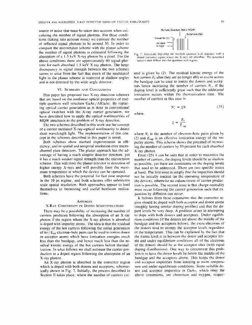
An X-ray photon is absorbed in the converter region which is doped with both donors and acceptors, schemat- ically shown in Fig. 7. Initially, the process described in Section I1 takes place, where the number of carriers cre-
Multiple Quantum Wells ( M O W )
1 [Substrate (Sb) Converter (C) 3
Incident -1 1 I I 1 1 1 x-rays -
Fig. 7 . Schematic depicting the multiple quantum well htructure with a doped converter region where the X-rays arc absorbed. The generated carriers then ditfuse into the quantum well region.
ated is given by (2). The residual kinetic energy of the hot carriers EL after they are no longer able to excite across the bandgap can be used to ionize the donors and accep- tors hence increasing the number of carriers N , , if the doping level is sufficiently great such that the additional ionization occurs within the thermalization time. The number of carriers in this case is
where
where N(. is the number of electron-hole pairs given by (2) and E,,, is an effective ionization energy of the im- purity atoms. This scheme shows the potential of increas- ing the number of carriers by 50 percent for each absorbed X-ray photon.
From (25) it can be seen that in order to maximize the number of carriers, the doping levels should be as shallow as possible, yet there are constraints on the doping levels that need to be addressed. There are two specific issues at hand. The first issue is simply that the impurities should not be initially ionized (at the operating temperature of the device), otherwise no enhancement of carrier produc- tion is possible. The second issue is that charge neutrality must occur following the carrier generation such that ex- pansion by diffusion can occur.
It follows from these constraints that the converter re- gion should be doped with both acceptor and donor atoms (roughly having similar doping profiles) and that the do- pant levels be very deep. A problem arises in attempting to dope with both donors and acceptors. Under equilib- rium conditions (if the donors are above the middle of the bandgap and the acceptors below), the extra electrons of the donors tend to occupy the acceptor levels regardless of the temperature. This can be explained by the fact that the Fermi level is in between the donor and acceptor lev- els and under equilibrium conditions all of the electrons of the donors should be at the acceptor sites (with equal doping distributions). One way to circumvent this prob- lem is to have the donor levels be below the middle of the bandgap and the acceptors above. This keeps the donor and acceptor impurities from ionizing at room tempera- ture and under equilibrium conditions. Some suitable do- nor and acceptor impurities in GaAs, which obey the above constraints, are chromium and oxygen, respec-
84 I E E E J O U R N A L OF Q U A N T U M ELECTRONICS. VOL 26, NO. 1 . JANUARY 1990
tivelY [221. Using these imUUritieS, we believe that an en- I171 J . L. Jewell. A. Scherer. S . L. McCall. A. C. Gossard, and J . H. ~. - - hancement of 50 percent (as mentioned above) can be at- tained.
English. "GaAs-AIAs monolithic microresonator arrays." Appl. Phys. Lerr., vol. 51, pp. 94-96. 1987.
[I81 J . L. Jewell, Y. H. Lee, M. Warren, H. M. Gibbs. N . Peyghambar-
ACKNOWLEDGMENT ian. A. C. Gossard. and W. Wiegmann. "3-pJ, 82-MHz optical logic gates in a room-temperature GaAs-AIGaAs multiple-quantum-well etalon," Appl. Phys.-Lett.. vol. 46, pp. 918-920. i985:
1191 Y. H. Lee, H. M. Gibbs. J . L. Jewell, J . F. Duffy. T . Venkatesan, A. C. Gossard. W. Wiegmann. and J . H. English, "Speed and effec-
The authors would like to thank J . Jewel13 E. Ippen, G . Dresselhaus, M. Dresselhaus. M. Muendel. and S . Kau- shik for both helpful and stimulating discussions.
REFERENCES M. J . Eckart. R. L. Hanks. J . D. Kilkenny, R. Pasha, J . D. Wied- wald. and J . D. Hares. "Largc-area 200-ps gated microchannel plate detector." Rev. Sci. Insrrum.. vol. 57. 1986. A. G. Michette, Optical Sy.sfetn.s f o r Soft X-Rays. New York: Plenum, 1986. pp. 27-28. G . W . Fraser. "The soft x-ray quantum detection efticiency of mi- crochannel plates." Nucl. Iristrum. Methods, vol. 195, pp. 523-538. 1982. J . L. Wira. "Microchannel plate detectors." Nu(./. Insrrum. Mrrh- od.\, vol. 162. pp. 587-601. 1979. H Haug and S . Schmitt-Rink. "Basic mechanisms of thc optical non- linearitie\ of semiconductors near the band edge." J . Opt. Soc. Amer. B. vol. 2. 1985. N. Peyghambarian and H. M. Gibbs. "Optical nonlinearity, bistabil- i ty . and signal processing in semiconductors." J . Opr. Soc. Atner. B. vnl. 2. pp. 1215-1227. 1985. D. S . Chemla and D. A. B. Miller, "Room-temperature excitonic nonlinear-optical etfects in scmiconductor quantum-well structures.'' J . Opt . Soc. Amer. B. vol. 2 . pp. 1155-1173. 1985. Y. H. Lee. A. Chavez-Pirson. S . W. Koch. H. M. Gibbs. S . H. Park, J. Morhange. A . Jeffery. N. Peyghambarian. L. Banyai. A. C. Gos- sard. and W. Wiegmann. "Room-temperature optical nonlinearities in GaAs." P h ~ s . Rei,. Lerr., vol. 57. pp. 2446-2449, 1986. B. L. Henke e / al.. "Low-energy X-ray interaction coefficients." Aromic. Dtrtu N u d . Dura Tuhles, vol. 27. pp. 2-1 15, 1982. C. A. Klein. "Bandgap dependence and related features of radiation ionization energies in Femiconductors." J . Appl. Phys., vol. 39, pp. 2029-2038, 1968. C. J . Wu and D. B. Wittry. "Investigation of minority-carrier diffu- sion lengths by electron bornbardmcnt of Schottky barriers." J . Appl . P h y s . . vol. 49. pp. 2827-2836. 1978. R. C . Alig. S . Bloom. and C. W. Struck, "Scattering by ionization and phonon emission in semiconductors.'' Phys. Rev. E . , vol. 22. pp. 5565-5582. 1980. D. S . Chemla. D. A . B . Miller. P. W. Smith, A. C. Gossard. and W . Wiegmann. "Room temperature excitonic nonlinear absorption and refraction in GaAs/AIGaAs multiple quantum well structures," IEEE J . Quuiitut~i Electroii., vol. QE-20. pp. 265-275. 1984. S Schmitt-Rink. D. S . Chemla. and D. A. B. Miller. "Theory of transient excitonic optical nonlinearities in semiconductor quantum- well \tructures," Phys. Ret,. B . vol. 32. pp. 6601-6609, 1985. R. R . Adler. A. C . Smith, and R. L. Longini, Inrroducrion ro Semi- conductor Physics. D. Miller. D. Chemla. D. Eilenberger. and P. Smith, "Large room- tenipcrature optical nonlinearity in GaAs/GaAIAs multiple quantum well structures.'' Appl . Phys. Let t . . v o l . 41. pp. 679-681, 1982.
New York: Wiley. 1964, pp. 141-191.
tiveness of windowless GaAs etalons as optical logic gates," Appl. Phys. Letr.. vol. 49. pp. 486-488, 1986.
1201 W. D. Barfeld. G. D. Koontz, and W. F . Huebner. "Fits to new calculations of photoionization cross sections for low-Z elements," J . Quantum Specrrosc. Radiat. Trunsfer., vol. 12. pp. 1409-1433, 1972.
1211 J . Hegarty. M. D. Sturge, C. Weisbuch, A. C . Gossard, and W. Wiegmann. "Resonant Rayleigh scattering from an inhomogeneously broadened transition: A new probe of the homogeneous linewidth." Phys. Rers. Letr.. vol. 49. pp. 930-932, 1982.
[22] A. G. Milnes. Deep Impurities i n Semiconductors. New York: Wiley, 1973.
Cristopher C. Eugster was born in San Antonio. TX, on October 1 I , 1965. He received the B.S. degree from Texas A & M University, College Station, and the M.S. degree from the Massachu- setts Institute of Technology. Cambridge, both in electrical engineering, in May 1987 and January 1989, respectively.
He is currently working towards the Ph.D. de- gree at M.I.T. in electrical engineering. His re- search interests include X-ray-induced nonlinear- ities in semiconductors as well as novel quantum
Mr. Eugster is a member of Tau Beta Pi. Phi Kappa Phi, and Sigma Xi. effect devices. He has two patents pending in these areas.
During the course of his master's work he was a TRW Fellow.
Peter L. Hagelstein (A'87) was born in Ingle- wood, CA, on July 31, 1954. He received the B . S . , M.S. (1976). andPh.D. (198l)degreesfrom the Massachusetts Institute of Technology, Cam- bridge.
He was involved in X-ray laser research at the Lawrence Livermore National Laboratory in the late 1970's and early 1980's. Since 1986 he has been on the faculty at M.I .T. in the Department of Electrical Engineering and Computer Science. His current research interests include X-ray lasers
and associated atomic and plasma physics, X-ray detection, and the pos- sibility of low-energy coherent nuclear reactions.
Dr. Hagelstein is a member of American Physical Society and the Amer- ican Association for the Advancement of Science. In 1984 he won the Er- nest 0. Lawrence Prize for contributions to national defense.