towards self-powering touch/flex-sensitive oled systems
TRANSCRIPT
IEEE SENSORS JOURNAL, VOL. 11, NO. 11, NOVEMBER 2011 2771
Towards Self-Powering Touch/Flex-SensitiveOLED Systems
Yindar Chuo, Clint Landrock, Badr Omrane, Jeydmer Aristizabal, Jasbir N. Patel,Marcin Marzencki, Member, IEEE, and Bozena Kaminska, Member, IEEE
Abstract—In this work, we present a novel design for an organiclight-emitting system integrated with a mechanical energy har-vesting and energy storage polymer films (patent pending). Thesystem is configured into multiple stacked layers to form a thin,flexible, and lightweight assembly. The thin “film-like” device canbe deformed and flexed to generate energy up to 0.5 mW within100 s with ease. This platform technology finds applications inenergy harvesting displays, electronic papers, key-input-pads,novel packaging, smart-IDs, disposable lab-on-a-chip optomi-crofluidic systems, and much more. Results on the energy storagecharacteristics of the ionic polymer-metal composite film, theperformance of a polyfluorene-based organic light-emitting de-vice, and the mechanical energy transduction of the piezoelectricpolymer energy harvester are presented. The polymeric nature ofthis platform system further makes it suitable for roll-to-roll printmanufacturing, supporting applications requiring high volumeand low cost.
Index Terms—Energy harvesting, integration, micro-opticalsystems, microsensors, organic light-emitting diode (OLED),polymers.
I. INTRODUCTION
O NE OF THE rising challenges in microsensors and mi-crosystems deployment in wireless, portable, or wear-
able applications, is in choosing the energy source. For mostmicrosystems, the energy required to power its microprocessoris negligible; however, its sensor and actuator elements mayconsume significant amounts of power at orders of magnitudehigher. In certain applications that require a lightweight smallfootprint system to operate autonomously, often the primary en-ergy source is a battery that is itself substantially larger thanthe core system. Many recent efforts have included energy har-vesting as a supplementary powering source. Integrated solarcells on outdoor wireless sensor nodes, and vibration energyharvesting used on automotive sensor units are some commonlyfound examples. Assisted powering of microdevices through en-ergy harvesting is inherently a phenomenon that requires the
Manuscript received January 31, 2011; revised June 06, 2011; accepted June14, 2011. Date of publication June 23, 2011; date of current version October21, 2011. This research is partly supported by the Natural Sciences and Engi-neering Research Council of Canada. This is an expanded paper from the IEEESENSORS 2010 Conference. The associate editor coordinating the review ofthis paper and approving it for publication was Dr. Thomas Kenny.
The authors are with the Centre for Integrative Biomedical EngineeringResearch, Department of Engineering Science, at Simon Fraser University,Vancouver, Canada (e-mail: [email protected]; [email protected]; [email protected];[email protected]; [email protected]; [email protected]; [email protected]).
Color versions of one or more of the figures in this paper are available onlineat http://ieeexplore.ieee.org.
Digital Object Identifier 10.1109/JSEN.2011.2160337
matching of function and environment, and hence, there is nouniversal solution (e.g., photovoltaic energy harvesting is notsuitable with a subcutaneous implantable glucose sensor).
Recent studies have shown that ionic polymer metal com-posites (IPMC) as dry energy storage films exhibit supercapac-itor and rechargeable battery like characteristics [1]. The par-ticular polymer electrolyte considered is the perfluorosulfonicacid (PSFA) based “Nafion” films from DuPont. Without hydra-tion, it can be used in the construction of energy storage IPMCs,and can be conveniently shaped and scaled into any dimensionsor geometries, and further operated at high-temperature condi-tions [2]. Nafion is traditionally also known for its electroactivecharacteristics in generating or sensing large mechanical defor-mations for industrial, space, and biomedical applications [3],[4]; however, it has been demonstrated that Nafion’s ability toconvert mechanical energy to electrical energy is generally in-ferior to piezoelectric polymers such as polyvinylidene fluoride(PVDF), by orders of magnitudes [5], [6]. The polymeric na-ture of both Nafion and PVDF makes them suitable in print-type or other forms of low-cost manufacturing that is inherentlycompatible with certain other polymer electronics. Combininga Nafion-based energy storage film with a PVDF-based energyharvesting film thus provides an attractive, low-cost, alterna-tive/supplementary energy solution in several organic and mi-croelectronic sensor systems.
Organic light-emitting diodes (OLEDs) are a technology thathas began to replace traditional light sources in various sensorsystems, particularly those seeking lower manufacturing costs,light weight, thin, and flexible profiles. For example, severalOLED-based microfluidic lab-on-a-chip (LOC) systems for dis-posable fluorescence-based chemical detection have been de-scribed recently [7], [8]. The use of integrated OLEDs in aLOC reduces the cost of the systems by reducing the numberof external components (i.e., external light source) addition-ally required for analysis [8]. However, most LOC microsys-tems still require a power source (e.g., a battery) that is oftenmuch larger, bulkier, and higher cost than the detection moduleitself. A platform that integrates thin-film-energy-storage andthin-film-energy-harvesting together with OLEDs thus presentsan interesting combination in generating new devices and sys-tems that move towards self-powered organic electronic appli-cations. Several potential applications include, but are not lim-ited to: energy harvesting touch screen displays; electronic pa-pers; key-input pads; novel packaging; supplementary energysource to overall sensor systems; wake-up activation switches;smart-IDs; and disposable LOC optomicrofluidic systems.
1530-437X/$26.00 © 2011 IEEE
2772 IEEE SENSORS JOURNAL, VOL. 11, NO. 11, NOVEMBER 2011
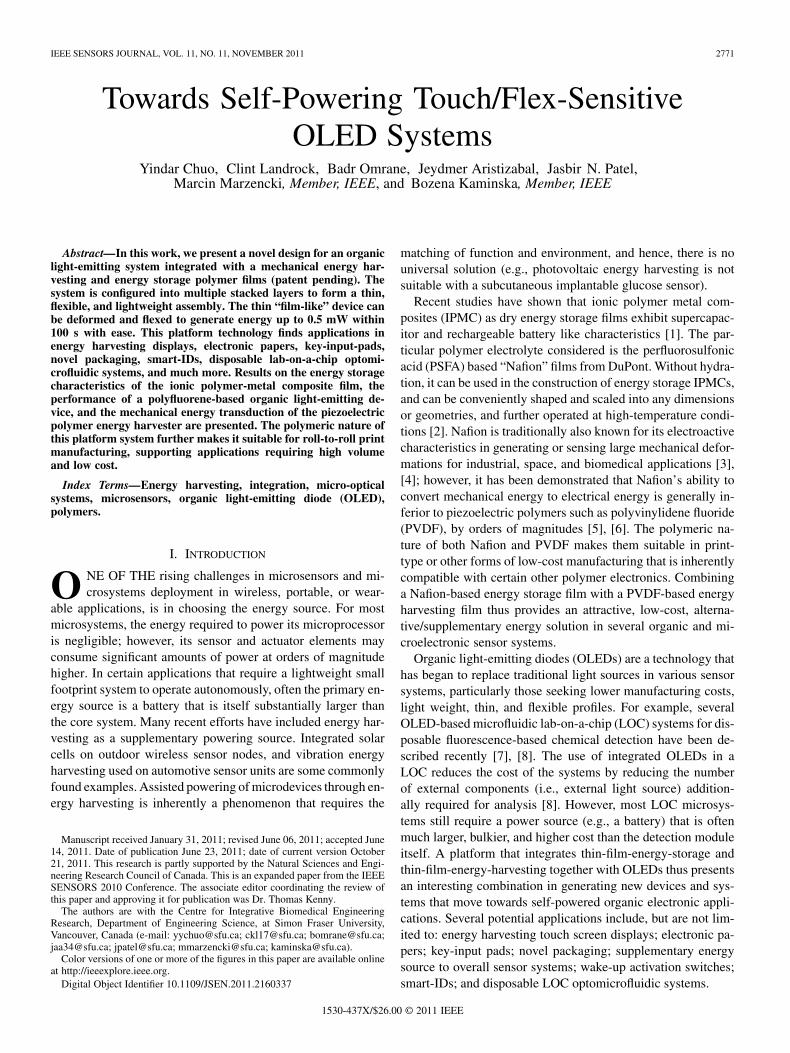
Fig. 1. Multilayer stacked configuration of the energy-harvesting OLEDplatform.
II. SYSTEM ARCHITECTURE
We present an integrated OLED and energy harvesting/storage multilayer platform (Fig. 1), where the touch/flex sen-sitive PVDF layers (energy harvesting) and the Nafion IPMClayers (energy storage) can be fabricated in parallel with theOLED then subsequently stacked and electrically connectedvia polymer lamination.
The energy storage Nafion-based IPMC films are mechani-cally flexible in nature, much similar to silicone rubber, and canbe configured into any thickness and dimensions based on theenergy storage capacity required. As described in the introduc-tion, the IPMC energy storage films can be operated similarlyto a supercapacitor or a small rechargeable battery.
The energy-harvesting PVDF films are also mechanicallyflexible. The PVDF films generate charges across its film bodywhen it is mechanically deformed (e.g., pressed or flexed). Inthe platform proposed, the energy transduced via the PVDFfilms is collected through a charge circuit into the IPMC en-ergy storage films. The stored energy can in turn serve as asupplementary, or even standalone, energy source to power amicrosystem.
OLEDs are formed by combining a number of very thin semi-conductive and conductive polymer and electrode layers. Be-cause of its thin polymer-conductor nature, and ability to be pat-terned into arrays of very small pixels, it is itself also mechan-ically flexible. The combination of the three flexible polymerelectronics layers in a stacked (3-D) configuration forms a thin,lightweight, flexible system that can potentially be manufac-tured completely through print-based fabrication.
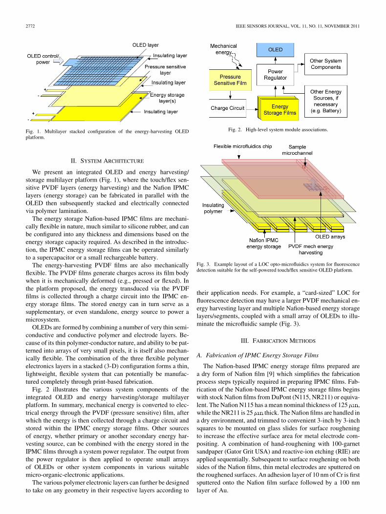
Fig. 2 illustrates the various system components of theintegrated OLED and energy harvesting/storage multilayerplatform. In summary, mechanical energy is converted to elec-trical energy through the PVDF (pressure sensitive) film, afterwhich the energy is then collected through a charge circuit andstored within the IPMC energy storage films. Other sourcesof energy, whether primary or another secondary energy har-vesting source, can be combined with the energy stored in theIPMC films through a system power regulator. The output fromthe power regulator is then applied to operate small arraysof OLEDs or other system components in various suitablemicro-organic-electronic applications.
The various polymer electronic layers can further be designedto take on any geometry in their respective layers according to
Fig. 2. High-level system module associations.
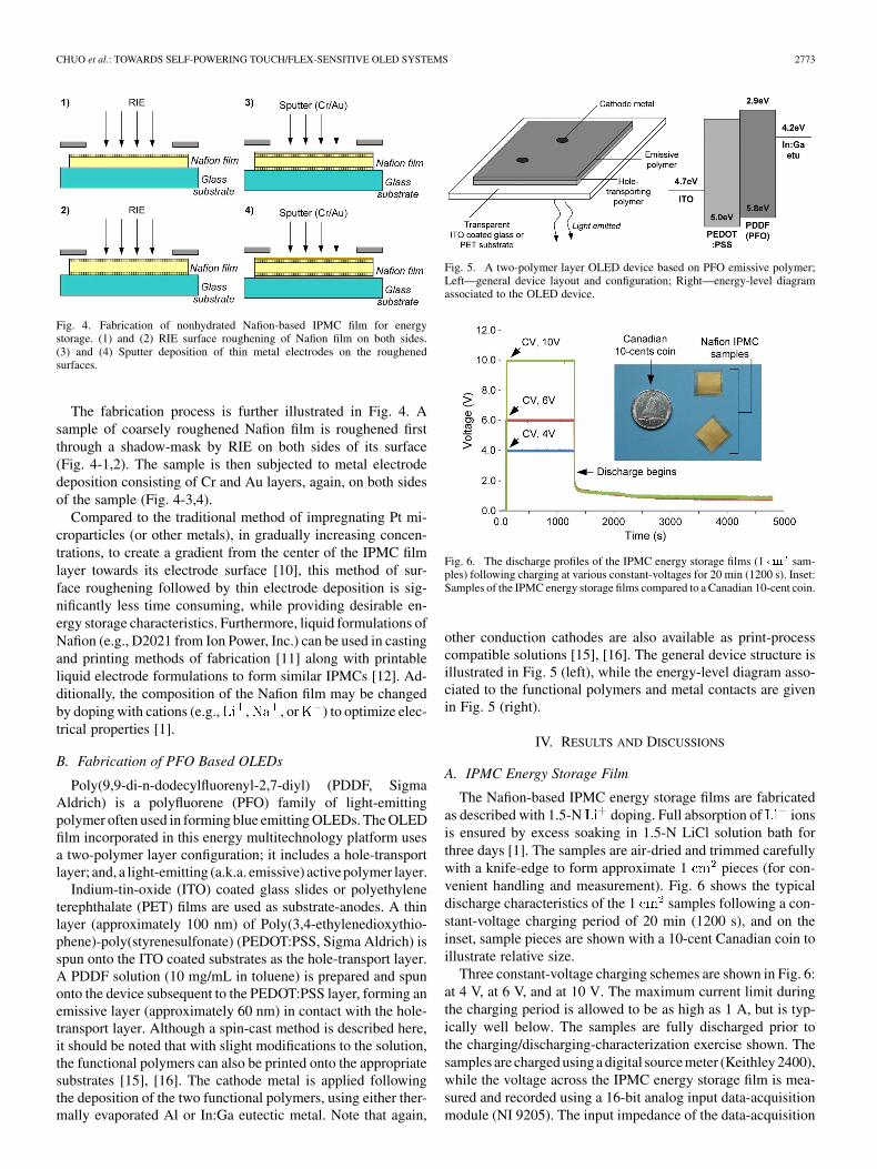
Fig. 3. Example layout of a LOC opto-microfluidics system for fluorescencedetection suitable for the self-powered touch/flex sensitive OLED platform.
their application needs. For example, a “card-sized” LOC forfluorescence detection may have a larger PVDF mechanical en-ergy harvesting layer and multiple Nafion-based energy storagelayers/segments, coupled with a small array of OLEDs to illu-minate the microfluidic sample (Fig. 3).
III. FABRICATION METHODS
A. Fabrication of IPMC Energy Storage Films
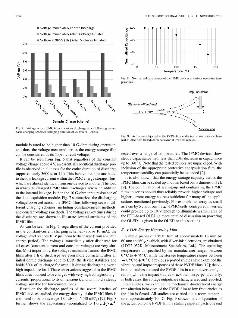
The Nafion-based IPMC energy storage films prepared area dry form of Nafion film [9] which simplifies the fabricationprocess steps typically required in preparing IPMC films. Fab-rication of the Nafion-based IPMC energy storage films beginswith stock Nafion films from DuPont (N115, NR211) or equiva-lent. The Nafion N115 has a mean nominal thickness of 125 ,while the NR211 is 25 thick. The Nafion films are handled ina dry environment, and trimmed to convenient 3-inch by 3-inchsquares to be mounted on glass slides for surface rougheningto increase the effective surface area for metal electrode com-positing. A combination of hand-roughening with 100-garnetsandpaper (Gator Grit USA) and reactive-ion etching (RIE) areapplied sequentially. Subsequent to surface roughening on bothsides of the Nafion films, thin metal electrodes are sputtered onthe roughened surfaces. An adhesion layer of 10 nm of Cr is firstsputtered onto the Nafion film surface followed by a 100 nmlayer of Au.
CHUO et al.: TOWARDS SELF-POWERING TOUCH/FLEX-SENSITIVE OLED SYSTEMS 2773
Fig. 4. Fabrication of nonhydrated Nafion-based IPMC film for energystorage. (1) and (2) RIE surface roughening of Nafion film on both sides.(3) and (4) Sputter deposition of thin metal electrodes on the roughenedsurfaces.
The fabrication process is further illustrated in Fig. 4. Asample of coarsely roughened Nafion film is roughened firstthrough a shadow-mask by RIE on both sides of its surface(Fig. 4-1,2). The sample is then subjected to metal electrodedeposition consisting of Cr and Au layers, again, on both sidesof the sample (Fig. 4-3,4).
Compared to the traditional method of impregnating Pt mi-croparticles (or other metals), in gradually increasing concen-trations, to create a gradient from the center of the IPMC filmlayer towards its electrode surface [10], this method of sur-face roughening followed by thin electrode deposition is sig-nificantly less time consuming, while providing desirable en-ergy storage characteristics. Furthermore, liquid formulations ofNafion (e.g., D2021 from Ion Power, Inc.) can be used in castingand printing methods of fabrication [11] along with printableliquid electrode formulations to form similar IPMCs [12]. Ad-ditionally, the composition of the Nafion film may be changedby doping with cations (e.g., , , or ) to optimize elec-trical properties [1].
B. Fabrication of PFO Based OLEDs
Poly(9,9-di-n-dodecylfluorenyl-2,7-diyl) (PDDF, SigmaAldrich) is a polyfluorene (PFO) family of light-emittingpolymer often used in forming blue emitting OLEDs. The OLEDfilm incorporated in this energy multitechnology platform usesa two-polymer layer configuration; it includes a hole-transportlayer; and, a light-emitting (a.k.a. emissive) active polymer layer.
Indium-tin-oxide (ITO) coated glass slides or polyethyleneterephthalate (PET) films are used as substrate-anodes. A thinlayer (approximately 100 nm) of Poly(3,4-ethylenedioxythio-phene)-poly(styrenesulfonate) (PEDOT:PSS, Sigma Aldrich) isspun onto the ITO coated substrates as the hole-transport layer.A PDDF solution (10 mg/mL in toluene) is prepared and spunonto the device subsequent to the PEDOT:PSS layer, forming anemissive layer (approximately 60 nm) in contact with the hole-transport layer. Although a spin-cast method is described here,it should be noted that with slight modifications to the solution,the functional polymers can also be printed onto the appropriatesubstrates [15], [16]. The cathode metal is applied followingthe deposition of the two functional polymers, using either ther-mally evaporated Al or In:Ga eutectic metal. Note that again,
Fig. 5. A two-polymer layer OLED device based on PFO emissive polymer;Left—general device layout and configuration; Right—energy-level diagramassociated to the OLED device.
Fig. 6. The discharge profiles of the IPMC energy storage films (1 �� sam-ples) following charging at various constant-voltages for 20 min (1200 s). Inset:Samples of the IPMC energy storage films compared to a Canadian 10-cent coin.
other conduction cathodes are also available as print-processcompatible solutions [15], [16]. The general device structure isillustrated in Fig. 5 (left), while the energy-level diagram asso-ciated to the functional polymers and metal contacts are givenin Fig. 5 (right).
IV. RESULTS AND DISCUSSIONS
A. IPMC Energy Storage Film
The Nafion-based IPMC energy storage films are fabricatedas described with 1.5-N doping. Full absorption of ionsis ensured by excess soaking in 1.5-N LiCl solution bath forthree days [1]. The samples are air-dried and trimmed carefullywith a knife-edge to form approximate 1 pieces (for con-venient handling and measurement). Fig. 6 shows the typicaldischarge characteristics of the 1 samples following a con-stant-voltage charging period of 20 min (1200 s), and on theinset, sample pieces are shown with a 10-cent Canadian coin toillustrate relative size.
Three constant-voltage charging schemes are shown in Fig. 6:at 4 V, at 6 V, and at 10 V. The maximum current limit duringthe charging period is allowed to be as high as 1 A, but is typ-ically well below. The samples are fully discharged prior tothe charging/discharging-characterization exercise shown. Thesamples are charged using a digital source meter (Keithley 2400),while the voltage across the IPMC energy storage film is mea-sured and recorded using a 16-bit analog input data-acquisitionmodule (NI 9205). The input impedance of the data-acquisition
2774 IEEE SENSORS JOURNAL, VOL. 11, NO. 11, NOVEMBER 2011
Fig. 7. Voltage across IPMC films at various discharge times following severalbasic charging schemes (charging duration of 20 min or 1200 s).
module is rated to be higher than 10 G-ohm during operation,and thus, the voltage measured across the energy storage filmcan be considered as its “open-circuit voltage.”
It can be seen from Fig. 6 that regardless of the constantvoltage charge above 4 V, an essentially identical discharge pro-file is observed in all cases for the entire duration of discharge(approximately 3600 s, or 1 h). This behavior can be attributedto the low leakage current within the IPMC energy storage films,which are almost identical from one device to another. The loadin which the charged IPMC films discharges across, in additionto the internal leakage, is then the 10 G-ohm input resistance ofthe data-acquisition module. Fig. 7 summarizes the dischargingvoltage observed across the IPMC films following several dif-ferent charging schemes, including constant-current methods,and constant-voltages methods. The voltages at key times duringthe discharge are shown to illustrate several attributes of theIPMC film.
As can be seen in Fig. 7, regardless of the current providedin the constant-current charging schemes (above 10 mA), thevoltage level reaches 10 V just prior to discharge (from a 20 mincharge period). The voltages immediately after discharge forall cases (constant-current and constant-voltage) are very sim-ilar. Most importantly, the voltages maintained across the IPMCfilms after 1 h of discharge are even more consistent; after aninitial ohmic discharge (due to ESR) the device stabilizes andholds 80% of its charge for over 1 h during discharging over ahigh impedance load. These observations suggest that the IPMCfilms does not need to be charged with very high voltages or highcurrents (proportional to its dimensions), and will hold a steadyvoltage suitable for low-current loads.
Based on the discharge profiles of the several batches ofIPMC devices studied, the energy density of the IPMC films isestimated to be on average 1.0 (40 mF/g) [9]. Fig. 8further shows the capacitance (normalized to 1.0 )
Fig. 8. Normalized capacitance of the IPMC devices at various operating tem-peratures.
Fig. 9. Actuation subjected to the PVDF film under test to study its mechan-ical-to-electrical transduction behavior at low frequencies.
tested over a range of temperatures. The IPMC devices showsteady capacitance with less than 20% decrease in capacitanceup to 160 C. Note that the tested devices are unpackaged. Withinclusion of the appropriate protective encapsulation film, thetemperature stability can potentially be extended [2].
It is also known that the energy storage capacity across theIPMC films can be scaled up or down based on its dimension [2],[9]. The combination of scaling-up and configuring the IPMCfilms in series should thus reliably provide higher voltage andhigher current energy sources sufficient for many of the appli-cations mentioned previously. For example, an array as smallas 2 cm by 5 cm of our 1 -IPMC-cells, configured in-series,could provide up to 10 V, enough to illuminate a small area ofthe PFO-based OLED (a more detailed discussion on poweringthe OLEDs is given in the OLED results section).
B. PVDF Energy Harvesting Film
Sample pieces of PVDF film of approximately 16 mm by60 mm and 60 -thick, with silver-ink electrodes, are obtained(LDT2-052K, Measurement Specialties, Ltd.). The operatingtemperature as specified by the manufacturer ranges between0 C to C, while the storage temperature ranges between
C to C. Previous reported studies have examined thevibration and impact responses of these PVDF films [17]; the vi-bration studies actuated the PVDF film in a cantilever configu-ration, while the impact studies struck the film perpendicularly;in both cases, the voltage outputs are characterized and reported.In our studies, we examine the mechanical-to-electrical energytransduction behaviors of the PVDF film at low frequencies asthe film is flexed. All studies are carried out a room-tempera-ture, approximately 20 C. Fig. 9 shows the configuration ofthe actuation to the PVDF film: a striking input impacts one end
CHUO et al.: TOWARDS SELF-POWERING TOUCH/FLEX-SENSITIVE OLED SYSTEMS 2775
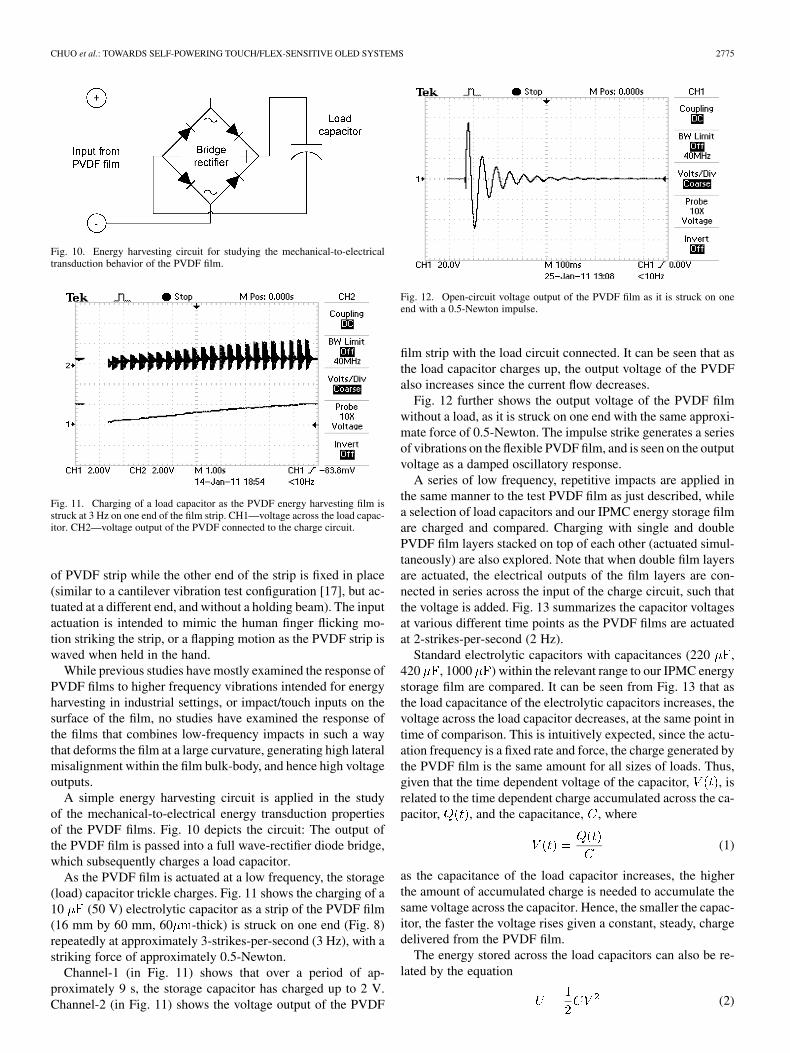
Fig. 10. Energy harvesting circuit for studying the mechanical-to-electricaltransduction behavior of the PVDF film.
Fig. 11. Charging of a load capacitor as the PVDF energy harvesting film isstruck at 3 Hz on one end of the film strip. CH1—voltage across the load capac-itor. CH2—voltage output of the PVDF connected to the charge circuit.
of PVDF strip while the other end of the strip is fixed in place(similar to a cantilever vibration test configuration [17], but ac-tuated at a different end, and without a holding beam). The inputactuation is intended to mimic the human finger flicking mo-tion striking the strip, or a flapping motion as the PVDF strip iswaved when held in the hand.
While previous studies have mostly examined the response ofPVDF films to higher frequency vibrations intended for energyharvesting in industrial settings, or impact/touch inputs on thesurface of the film, no studies have examined the response ofthe films that combines low-frequency impacts in such a waythat deforms the film at a large curvature, generating high lateralmisalignment within the film bulk-body, and hence high voltageoutputs.
A simple energy harvesting circuit is applied in the studyof the mechanical-to-electrical energy transduction propertiesof the PVDF films. Fig. 10 depicts the circuit: The output ofthe PVDF film is passed into a full wave-rectifier diode bridge,which subsequently charges a load capacitor.
As the PVDF film is actuated at a low frequency, the storage(load) capacitor trickle charges. Fig. 11 shows the charging of a10 (50 V) electrolytic capacitor as a strip of the PVDF film(16 mm by 60 mm, 60 -thick) is struck on one end (Fig. 8)repeatedly at approximately 3-strikes-per-second (3 Hz), with astriking force of approximately 0.5-Newton.
Channel-1 (in Fig. 11) shows that over a period of ap-proximately 9 s, the storage capacitor has charged up to 2 V.Channel-2 (in Fig. 11) shows the voltage output of the PVDF
Fig. 12. Open-circuit voltage output of the PVDF film as it is struck on oneend with a 0.5-Newton impulse.
film strip with the load circuit connected. It can be seen that asthe load capacitor charges up, the output voltage of the PVDFalso increases since the current flow decreases.
Fig. 12 further shows the output voltage of the PVDF filmwithout a load, as it is struck on one end with the same approxi-mate force of 0.5-Newton. The impulse strike generates a seriesof vibrations on the flexible PVDF film, and is seen on the outputvoltage as a damped oscillatory response.
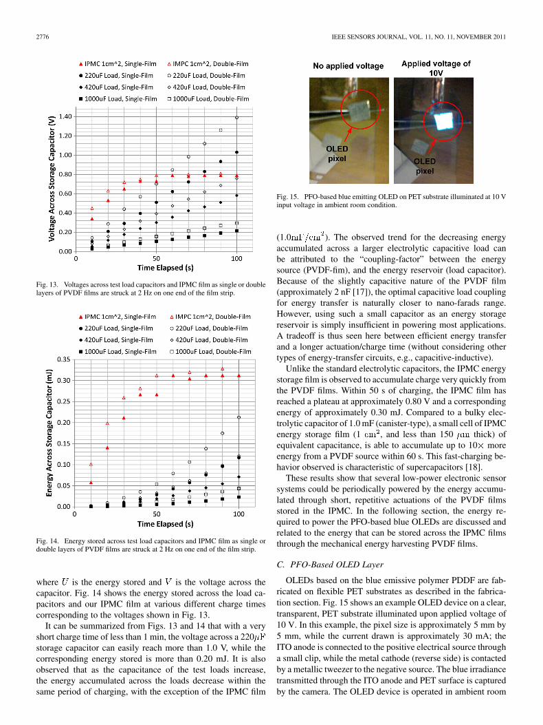
A series of low frequency, repetitive impacts are applied inthe same manner to the test PVDF film as just described, whilea selection of load capacitors and our IPMC energy storage filmare charged and compared. Charging with single and doublePVDF film layers stacked on top of each other (actuated simul-taneously) are also explored. Note that when double film layersare actuated, the electrical outputs of the film layers are con-nected in series across the input of the charge circuit, such thatthe voltage is added. Fig. 13 summarizes the capacitor voltagesat various different time points as the PVDF films are actuatedat 2-strikes-per-second (2 Hz).
Standard electrolytic capacitors with capacitances (220 ,420 , 1000 ) within the relevant range to our IPMC energystorage film are compared. It can be seen from Fig. 13 that asthe load capacitance of the electrolytic capacitors increases, thevoltage across the load capacitor decreases, at the same point intime of comparison. This is intuitively expected, since the actu-ation frequency is a fixed rate and force, the charge generated bythe PVDF film is the same amount for all sizes of loads. Thus,given that the time dependent voltage of the capacitor, , isrelated to the time dependent charge accumulated across the ca-pacitor, , and the capacitance, , where
(1)
as the capacitance of the load capacitor increases, the higherthe amount of accumulated charge is needed to accumulate thesame voltage across the capacitor. Hence, the smaller the capac-itor, the faster the voltage rises given a constant, steady, chargedelivered from the PVDF film.
The energy stored across the load capacitors can also be re-lated by the equation
(2)
2776 IEEE SENSORS JOURNAL, VOL. 11, NO. 11, NOVEMBER 2011
Fig. 13. Voltages across test load capacitors and IPMC film as single or doublelayers of PVDF films are struck at 2 Hz on one end of the film strip.
Fig. 14. Energy stored across test load capacitors and IPMC film as single ordouble layers of PVDF films are struck at 2 Hz on one end of the film strip.
where is the energy stored and is the voltage across thecapacitor. Fig. 14 shows the energy stored across the load ca-pacitors and our IPMC film at various different charge timescorresponding to the voltages shown in Fig. 13.
It can be summarized from Figs. 13 and 14 that with a veryshort charge time of less than 1 min, the voltage across a 220storage capacitor can easily reach more than 1.0 V, while thecorresponding energy stored is more than 0.20 mJ. It is alsoobserved that as the capacitance of the test loads increase,the energy accumulated across the loads decrease within thesame period of charging, with the exception of the IPMC film
Fig. 15. PFO-based blue emitting OLED on PET substrate illuminated at 10 Vinput voltage in ambient room condition.
(1.0 ). The observed trend for the decreasing energyaccumulated across a larger electrolytic capacitive load canbe attributed to the “coupling-factor” between the energysource (PVDF-fim), and the energy reservoir (load capacitor).Because of the slightly capacitive nature of the PVDF film(approximately 2 nF [17]), the optimal capacitive load couplingfor energy transfer is naturally closer to nano-farads range.However, using such a small capacitor as an energy storagereservoir is simply insufficient in powering most applications.A tradeoff is thus seen here between efficient energy transferand a longer actuation/charge time (without considering othertypes of energy-transfer circuits, e.g., capacitive-inductive).
Unlike the standard electrolytic capacitors, the IPMC energystorage film is observed to accumulate charge very quickly fromthe PVDF films. Within 50 s of charging, the IPMC film hasreached a plateau at approximately 0.80 V and a correspondingenergy of approximately 0.30 mJ. Compared to a bulky elec-trolytic capacitor of 1.0 mF (canister-type), a small cell of IPMCenergy storage film (1 , and less than 150 thick) ofequivalent capacitance, is able to accumulate up to 10 moreenergy from a PVDF source within 60 s. This fast-charging be-havior observed is characteristic of supercapacitors [18].
These results show that several low-power electronic sensorsystems could be periodically powered by the energy accumu-lated through short, repetitive actuations of the PVDF filmsstored in the IPMC. In the following section, the energy re-quired to power the PFO-based blue OLEDs are discussed andrelated to the energy that can be stored across the IPMC filmsthrough the mechanical energy harvesting PVDF films.
C. PFO-Based OLED Layer
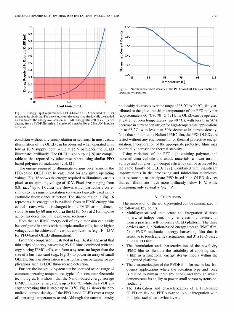
OLEDs based on the blue emissive polymer PDDF are fab-ricated on flexible PET substrates as described in the fabrica-tion section. Fig. 15 shows an example OLED device on a clear,transparent, PET substrate illuminated upon applied voltage of10 V. In this example, the pixel size is approximately 5 mm by5 mm, while the current drawn is approximately 30 mA; theITO anode is connected to the positive electrical source througha small clip, while the metal cathode (reverse side) is contactedby a metallic tweezer to the negative source. The blue irradiancetransmitted through the ITO anode and PET surface is capturedby the camera. The OLED device is operated in ambient room
CHUO et al.: TOWARDS SELF-POWERING TOUCH/FLEX-SENSITIVE OLED SYSTEMS 2777
Fig. 16. Energy input requirements a PFO-based OLED (operated at 10 V)related to its pixel size. The curve indicates the energy required, while the shadedarea indicates the energy available on an IPMC energy film cell (1 �� ) aftercharing from a PVDF film strip (16 mm by 60 mm) for 60 s at 2 Hz, 5 N, impulseactuation.
condition without any encapsulation or sealants. In most cases,illumination of the OLED can be observed when operated at aslow as 10 V supply input, while at 15 V or higher, the OLEDilluminates brilliantly. The OLED light output [19] are compa-rable to that reported by other researchers using similar PFObased polymer formulations [20], [21].
The energy required to illuminate various pixel sizes of thePFO-based OLED can be calculated for any given operatingvoltage. Fig. 16 shows the energy required to illuminate variouspixels at an operating voltage of 10 V. Pixel sizes ranging from0.01 up to 1.0 are shown, which particularly corre-sponds to the range of excitation spot-sizes typically used in mi-crofluidic fluorescence detection. The shaded region in Fig. 16represents the energy that is available from an IPMC energy filmcell of 1 , when it is charged from a PVDF strip of dimen-sions 16 mm by 60 mm (60 thick) for 60 s at 2 Hz impulseaction (as described in the previous sections).
Note that an IPMC energy cell of any dimension can easilybe configured in series with multiple smaller cells, hence highervoltages can be achieved for various applications (e.g., 10–15 Vfor PFO-based OLED illumination).
From the comparison illustrated in Fig. 16, it is apparent thatthin strips of energy harvesting PVDF films combined with en-ergy storing IPMC cells, can form a system, no larger than thesize of a business card (e.g., Fig. 3), to power an array of smallOLEDs. Such an observation is particularly encouraging for ap-plications such as LOC fluorescence detection.
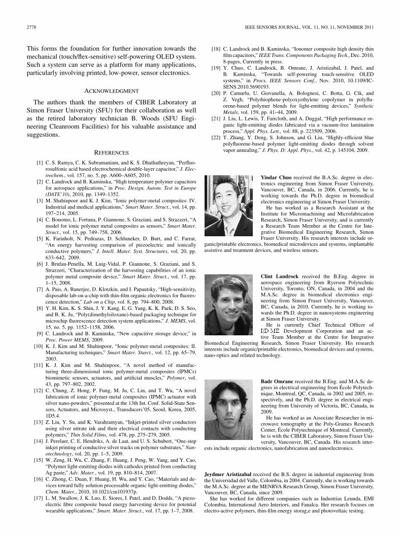
Further, the integrated system can be operated over a range ofcommon operating temperatures typical for consumer electronictechnologies. It is shown that the Nafion-based energy storageIPMC film is extremely stable up to 100 C, while the PVDF en-ergy harvesting film is stable up to 70 C. Fig. 17 shows the nor-malized current density of the PFO-based OLED over a rangeof operating temperatures tested. Although the current density
Fig. 17. Normalized current density of the PFO-based OLED as a function ofoperating temperature.
noticeably decreases over the range of 35 C to 90 C, likely at-tributed to the glass transition temperature of the PFO polymer(approximately 60 C to 70 C) [21], the OLED can be operatedat extreme room temperatures (up 40 C), with less than 90%decrease in current density, or for high-temperature applicationsup to 65 C, with less than 50% decrease in current density.Note that similar to the Nafion-IPMC film, the PFO-OLEDs aretested without any environmental or thermal protective encap-sulation. Incorporation of the appropriate protective films maypotentially increase the thermal stability.
Using variations of the PFO light-emitting polymer, andmore efficient cathode and anode materials, a lower turn-onvoltage and a higher light-output efficiency can be achieved forthe same family of OLEDs [22]. Combined with significantimprovements in the processing and fabrication techniques,it is reasonable to anticipate PFO-based blue OLED devicesthat can illuminate much more brilliantly below 10 V, whileconsuming only several .
V. CONCLUSION
The innovation of the work presented can be summarized inthe following key points.
• Multilayer-stacked architecture and integration of three,otherwise independent, polymer electronic devices, toform a practical self-powering OLED platform. The threedevices are: 1) a Nafion-based energy storage IPMC film;2) a PVDF mechanical energy harvesting film that issensitive to touch and flex actuations; and 3) a PFO-basedblue OLED film.
• The formulation and characterization of the novel dryIPMC film to illustrate the suitability of applying sucha film as a functional energy storage media within theintegrated platform.
• The characterization of the PVDF film for use in low-fre-quency applications where the actuation type and forceis related to human input (by hand), and through whichdemonstrates its ability to power small sensor systems pe-riodically.
• The fabrication and characterization of a PFO-basedOLED on flexible PET substrate to suit integration withmultiple stacked co-device layers.
2778 IEEE SENSORS JOURNAL, VOL. 11, NO. 11, NOVEMBER 2011
This forms the foundation for further innovation towards themechanical (touch/flex-sensitive) self-powering OLED system.Such a system can serve as a platform for many applications,particularly involving printed, low-power, sensor electronics.
ACKNOWLEDGMENT
The authors thank the members of CIBER Laboratory atSimon Fraser University (SFU) for their collaboration as wellas the retired laboratory technician B. Woods (SFU Engi-neering Cleanroom Facilities) for his valuable assistance andsuggestions.
REFERENCES
[1] C. S. Ramya, C. K. Subramaniam, and K. S. Dhathathreyan, “Perfluo-rosulfonic acid based electrochemical double-layer capacitor,” J. Elec-trochem., vol. 157, no. 5, pp. A600–A605, 2010.
[2] C. Landrock and B. Kaminska, “High temperature polymer capacitorsfor aerospace applications,” in Proc. Design, Autom. Test in Europe(DATE’10), 2010, pp. 1349–1352.
[3] M. Shahinpoor and K. J. Kim, “Ionic polymer-metal composites: IV.Industrial and medical applications,” Smart Mater. Struct., vol. 14, pp.197–214, 2005.
[4] C. Bonomo, L. Fortuna, P. Giannone, S. Graziani, and S. Strazzeri, “Amodel for ionic polymer metal composites as sensors,” Smart Mater.Struct., vol. 15, pp. 749–758, 2006.
[5] K. Farinholt, N. Pedrazas, D. Schluneker, D. Burt, and C. Farrar,“An energy harvesting comparison of piezoelectric and ionicallyconductive polymers,” J. Intell. Mater. Syst. Structures, vol. 20, pp.633–642, 2009.
[6] J. Brufau-Penella, M. Luig-Vidal, P. Giannone, S. Graziani, and S.Strazzeri, “Characterization of the harvesting capabilities of an ionicpolymer metal composite device,” Smart Mater. Struct., vol. 17, pp.1–15, 2008.
[7] A. Pais, A. Banerjee, D. Klotzkin, and I. Papautsky, “High-sensitivity,disposable lab-on-a-chip with thin-film organic electronics for fluores-cence detection,” Lab on a Chip, vol. 8, pp. 794–800, 2008.
[8] Y. H. Kim, K. S. Shin, J. Y. Kang, E. G. Yang, K. K. Paek, D. S. Seo,and B. K. Ju, “Poly(dimethylsiloxane)-based packaging technique formicrochip fluorescence detection system applications,” J. MEMS, vol.15, no. 5, pp. 1152–1158, 2006.
[9] C. Landrock and B. Kaminska, “New capacitive storage device,” inProc. Power MEMS, 2009.
[10] K. J. Kim and M. Shahinpoor, “Ionic polymer-metal composites: II.Manufacturing techniques,” Smart Mater. Sturct., vol. 12, pp. 65–79,2003.
[11] K. J. Kim and M. Shahinpoor, “A novel method of manufac-turing three-dimensional ionic polymer-metal composites (IPMCs)biomimetic sensors, actuators, and artificial muscles,” Polymer, vol.43, pp. 797–802, 2002.
[12] C. Chung, Z. Hong, P. Fung, M. Ju, C. Lin, and T. Wu, “A novelfabrication of ionic polymer-metal composites (IPMC) actuator withsilver nano-powders,” presented at the 13th Int. Conf. Solid-State Sen-sors, Actuators, and Microsyst., Transducers’05, Seoul, Korea, 2005,1D5.4.
[13] Z. Liu, Y. Su, and K. Varahramyan, “Inkjet-printed silver conductorsusing silver nitrate ink and their electrical contacts with conductingpolymers,” Thin Solid Films, vol. 478, pp. 275–279, 2005.
[14] J. Perelaer, C. E. Hendriks, A. de Laat, and U. S. Schubert, “One-stepinkjet printing of conductive silver tracks on polymer substrates,” Nan-otechnology, vol. 20, pp. 1–5, 2009.
[15] W. Zeng, H. Wu, C. Zhang, F. Huang, J. Peng, W. Yang, and Y. Cao,“Polymer light-emitting diodes with cathodes printed from conductingAg paste,” Adv. Mater., vol. 19, pp. 810–814, 2007.
[16] C. Zhong, C. Duan, F. Huang, H. Wu, and Y. Cao, “Materials and de-vices toward fully solution processable organic light-emitting diodes,”Chem. Mater., 2010, 10.1021/cm101937p.
[17] L. M. Swallow, J. K. Luo, E. Siores, I. Patel, and D. Dodds, “A piezo-electric fibre composite based energy harvesting device for potentialwearable applications,” Smart. Mater. Struct., vol. 17, pp. 1–7, 2008.
[18] C. Landrock and B. Kaminska, “Ionomer composite high density thinfilm capacitors,” IEEE Trans. Components Packaging Tech., Dec. 2010,8-pages, Currently in press.
[19] Y. Chuo, C. Landrock, B. Omrane, J. Aristizabal, J. Patel, andB. Kaminska, “Towards self-powering touch-sensitive OLEDsystems,” in Procs. IEEE Sensors Conf., Nov. 2010, 10.1109/IC-SENS.2010.5690193.
[20] P. Camurlu, U. Giovanella, A. Bolognesi, C. Botta, G. Cik, andZ. Vegh, “Polythiophene-polyoxyethylene copolymer in polyflu-orene-based polymer blends for light-emitting devices,” SyntheticMetals, vol. 159, pp. 41–44, 2009.
[21] J. Liu, L. Lewis, T. Faircloth, and A. Duggal, “High performance or-ganic light-emitting diodes fabricated via a vacuum-free laminationprocess,” Appl. Phys. Lett., vol. 88, p. 223509, 2006.
[22] T. Zhang, Y. Deng, S. Johnson, and G. Liu, “Highly-efficient bluepolyfluorene-based polymer light-emitting diodes through solventvapor annealing,” J. Phys. D: Appl. Phys., vol. 42, p. 145104, 2009.
Yindar Chuo received the B.A.Sc. degree in elec-tronics engineering from Simon Fraser University,Vancouver, BC, Canada, in 2006. Currently, he isworking towards the Ph.D. degree in biomedicalelectronics engineering at Simon Fraser University.
He has worked as a Research Assistant at theInstitute for Micromachining and MicrofabricationResearch, Simon Fraser University, and is currentlya Research Team Member at the Centre for Inte-grative Biomedical Engineering Research, SimonFraser University. His research interests include or-
ganic/printable electronics, biomedical microdevices and systems, implantableassistive and treatment devices, and wireless sensors.
Clint Landrock received the B.Eng. degree inaerospace engineering from Ryerson PolytechnicUniversity, Toronto, ON, Canada, in 2004 and theM.A.Sc. degree in biomedical electronics engi-neering from Simon Fraser University, Vancouver,BC, Canada, in 2010. Currently, he is working to-wards the Ph.D. degree in nanosystems engineeringat Simon Fraser University.
He is currently Chief Technical Officer of������ Development Corporation and an ac-tive Team Member at the Centre for Integrative
Biomedical Engineering Research, Simon Fraser University. His researchinterests include organic/printable electronics, biomedical devices and systems,nano-optics and related technology.
Badr Omrane received the B.Eng. and M.A.Sc de-grees in electrical engineering from École Polytech-nique, Montreal, QC, Canada, in 2002 and 2005, re-spectively, and the Ph.D. degree in electrical engi-neering from University of Victoria, BC, Canada, in2009.
He has worked as an Associate Researcher in mi-crowave tomography at the Poly-Grames ResearchCenter, École Polytechnique of Montreal. Currently,he is with the CIBER Laboratory, Simon Fraser Uni-versity, Vancouver, BC, Canada. His research inter-
ests include organic electronics, nanofabrication and nanoelectronics.
Jeydmer Aristizabal received the B.S. degree in industrial engineering fromthe Universidad del Valle, Colombia, in 2004. Currently, she is working towardsthe M.A.Sc. degree at the MENRVA Research Group, Simon Fraser University,Vancouver, BC, Canada, since 2009.
She has worked for different companies such as Industrias Leunda, EMIColombia, International Aero Interiors, and Fanalca. Her research focuses onelectro-active polymers, thin-film energy storag,e and photovoltaic testing.
CHUO et al.: TOWARDS SELF-POWERING TOUCH/FLEX-SENSITIVE OLED SYSTEMS 2779
Jasbir N. Patel received the B.Eng. degree inelectrical engineering from Gujarat University,Ahmedabad, Gujarat, India, in 1998 and the M.E.Sc.degree in electrical and computer engineering withspecialization in mixed-signal VLSI design from theUniversity of Western Ontario, London, ON, Canada,in 2005. Currently, he is working towards the Ph.D.degree at Simon Fraser University, Burnaby, BC,Canada.
He has worked as a Research and DevelopmentEngineer in the embedded software development and
process control instrumentation area for more than five years. Currently, he is aResearcher associated with the Centre for Integrative Biomedical EngineeringResearch (CIBER), Microinstrumentation Laboratory (mIL), and 4D Labs atSimon Fraser University. His research interests include biosensors, flexible andimplantable biosystems using polymer MEMS, polymer MEMS-based encap-sulation and packaging technologies and system level integration of polymer-based microsystems for biomedical and microfluidic applications.
Marcin Marzencki (M’08) graduated from theAGH University of Science and Technology, Cracow,Poland, in electronics and telecommunications. Hereceived the Ph.D. degree in microelectronics fromJoseph Fourier University, Grenoble, France, in2007. Now
Currently, he is with the CIBER Laboratory,Simon Fraser University, Vancouver, BC, Canada.His main fields of interest focus on environmentalenergy scavenging, distributed sensor systems, andMEMS devices.
Bozena Kaminska (M’88) received the Ph.D.degree from Warsaw University of Technology,Warsaw, Poland.
She has 30 years of academic and corporate ex-perience as a researcher, engineer, entrepreneur andeducator. She is presently a Professor and CanadaResearch Chair in Wireless Sensor Networks atSimon Fraser University, Vancouver, BC, Canada,focusing on the research and development of newsensors and nano/microsystems. She is a prolificinventor, having authored multiple patents and
more than 200 IEEE peer-reviewed publications in top scientific journals andconference proceedings.